

Product-to-Frequency
DELAY
2.5V
BAND GAP
REFERENCE
DTF
HPF
MULT
S1FS
VDD
DGND
DTF
LPF
2ND ORDER
MODULATOR
AGND REFOUT
G1
ADC1
ADC2
REFIN
V
1+
AD7750
2ND ORDER
MODULATOR
x2
x16
V
2+
S2
V
1–
V
2–
F2
CLKOUT
F1
F
OUT
REVP
CLKIN
ACDC
a
FEATURES
Two Differential Analog Input Channels
Product of Two Channels
Voltage-to-Frequency Conversion on a Single Channel
Real Power Measurement Capability
< 0.2% Error Over the Range 400% Ibasic to 2% Ibasic
Two or Four Quadrant Operation (Positive and
Negative Power)
Gain Select of 1 or 16 on the Current Channel (Channel 1)
Choice of On-Chip or External Reference
Choice of Output Pulse Frequencies Available
(Pins F1 and F2)
High Frequency Pulse Output for Calibration Purposes
(F
)
OUT
HPF on Current Channel for Offset Removal
Single 5 V Supply and Low Power
Converter
AD7750
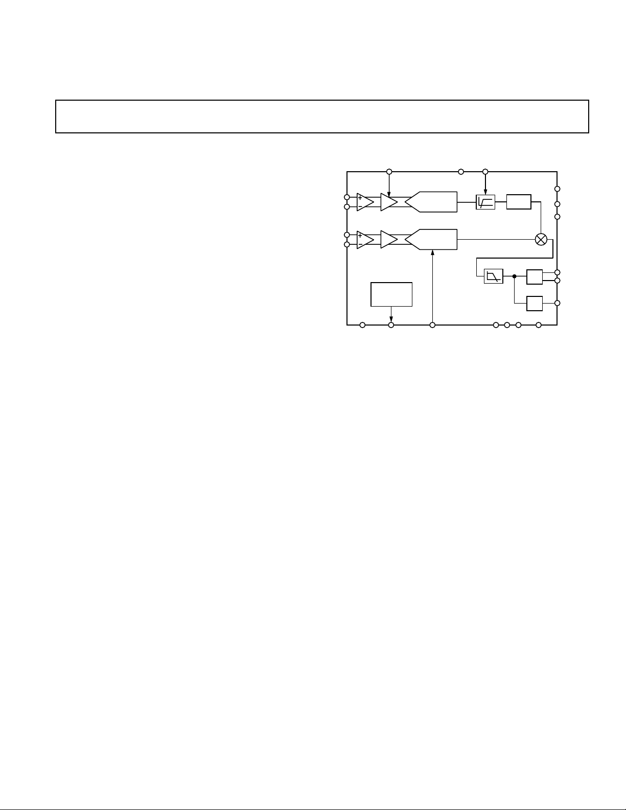
FUNCTIONAL BLOCK DIAGRAM
GENERAL DESCRIPTION
The AD7750 is a Product-to-Frequency Converter (PFC)
that can be configured for power measurement or voltage-tofrequency conversion. The part contains the equivalent of two
channels of A/D conversion, a multiplier, a digital-to-frequency
converter, a reference and other conditioning circuitry. Channel 1
has a differential gain amplifier with selectable gains of 1 or 16.
Channel 2 has a differential gain amplifier with a gain of 2. A highpass filter can be switched into the signal path of Channel 1 to
remove any offsets.
The outputs F1 and F2 are fixed width (275 ms) logic low going
pulse streams for output frequencies less than 1.8 Hz. A range
of output frequencies is available and the frequency of F1 and
F2 is proportional to the product of V
and V2. These outputs
1
PRODUCT HIGHLIGHTS
1. The part can be configured for power measurement or
voltage-to-frequency conversion.
2. The output format and maximum frequency is selectable;
from low-frequency outputs, suitable for driving stepper
motors, to higher frequency outputs, suitable for calibration
and test.
3. There is a reverse polarity indicator output that becomes
active when negative power is detected in the Magnitude
Only Mode.
4. Error as a % of reading over a dynamic range of 1000:1 is
< 0.3%.
are suitable for directly driving an electromechanical pulse
counter or full stepping two phase stepper motors. The outputs
can be configured to represent the result of four-quadrant multiplication (i.e., Sign and Magnitude) or to represent the result of
a two quadrant multiplication (i.e., Magnitude Only). In this
configuration the outputs are always positive regardless of the
input polarities. In addition, there is a reverse polarity indicator
output that becomes active when negative power is detected in
the Magnitude Only Mode, see Reverse Polarity Indicator.
The error as a percent (%) of reading is less than 0.3% over a
dynamic range of 1000:1.
The AD7750 is fabricated on 0.6 µ CMOS technology; a pro-
cess that combines low power and low cost.
REV. 0
Information furnished by Analog Devices is believed to be accurate and
reliable. However, no responsibility is assumed by Analog Devices for its
use, nor for any infringements of patents or other rights of third parties
which may result from its use. No license is granted by implication or
otherwise under any patent or patent rights of Analog Devices.
One Technology Way, P.O. Box 9106, Norwood, MA 02062-9106, U.S.A.
Tel: 781/329-4700 World Wide Web Site: http://www.analog.com
Fax: 781/326-8703 © Analog Devices, Inc., 1997

(VDD = 5 V 6 5%, AGND = 0 V, DGND = 0 V, REFIN = +2.5 V, CLKIN = 3.58 MHz
T
to T
AD7750–SPECIFICA TIONS
MIN
A Version
–408C to
Parameter +858C Units Test Conditions/Comments
ACCURACY
Measurement Error
1
Gain = 1 0.2 % Reading max Measured Over a Dynamic Range on Channel 1 of 500:1
0.3 % Reading max Measured Over a Dynamic Range on Channel 1 of 1000:1
Gain = 16 0.2 % Reading max Measured Over a Dynamic Range on Channel 1 of 500:1
0.4 % Reading max Measured Over a Dynamic Range on Channel 1 of 1000:1
Phase Error Between Channels CLKIN = 3.58 MHz, Line Frequency = 50 Hz
Phase Lead 40° (PF = +0.8) ±0.2 Degrees (°) max HPF Filter On, ACDC = 1
Phase Lag 60° (PF = –0.5) ±0.2 Degrees (°) max HPF Filter On, ACDC = 1
Feedthrough Between Channels HPF Filter On, ACDC = 1, Mode 3, Channel 1 = 0 V
Output Frequency Variation (F
) 0.0005 % Full-Scale max Channel 2 = 500 mV rms at 50 Hz
OUT
Power Supply Rejection HPF Filter On, ACDC = 1, Mode 3, Channel 1 = 0 V
Output Frequency Variation (F
) 0.03 % Full-Scale max Channel 2 = 500 mV rms, Power Supply Ripple
OUT
ANALOG INPUTS
Maximum Signal Levels ±1 V max On Any Input, V1+, V1–, V2+ and V2–. See Analog Inputs.
Input Impedance (DC) 400 kΩ min CLKIN = 3.58 MHz
Bandwidth 3.5 kHz typ CLKIN = 3.58 MHz, CLKIN/1024
Offset Error ±10 mV typ
Gain Error ±4 % Full-Scale typ
Gain Error Match ±0.3 % Full-Scale typ
REFERENCE INPUT
REF
Input Voltage Range 2.7 V max 2.5 V + 8%
IN
2.3 V min 2.5 V – 8%
Input Impedance 50 kΩ min
ON-CHIP REFERENCE Nominal 2.5 V
Reference Error ±200 mV max
Temperature Coefficient 55 ppm/°C typ
CLKIN
Input Clock Frequency 4.5 MHz max
2 MHz min
LOGIC INPUTS
FS, S1, S2, ACDC and G1
Input High Voltage, V
Input Low Voltage, V
Input Current, I
Input Capacitance, C
INL
IN
IN
INH
2.4 V min VDD = 5 V ± 5%
0.8 V max VDD = 5 V ± 5%
±10 µA max Typically 10 nA, VIN = 0 V to V
10 pF max
CLKIN
Input High Voltage, V
Input Low Voltage, V
LOGIC OUTPUTS
INH
INL
2
4 V min
0.4 V max
F1 and F2
Output High Voltage, V
OH
4.3 V min V
Output Low Voltage, V
OL
0.5 V max V
F
and REVP
OUT
Output High Voltage, V
OH
4 V min V
Output Low Voltage, V
OL
0.4 V max V
High Impedance Leakage Current ±10 µA max
High Impedance Capacitance 15 pF max
= –408C to +858C, ACDC = Logic High)
MAX
Channel 2 with Full-Scale Signal
250 mV at 50 Hz. See Figures 1 and 3.
I
= 8 mA
SOURCE
= 5 V
DD
I
= 8 mA
SINK
= 5 V
DD
I
= 1 mA
SOURCE
= 5 V ± 5%
DD
I
= 200 µA
SINK
= 5 V ± 5%
DD
DD
–2– REV. 0

AD7750
WARNING!
ESD SENSITIVE DEVICE
A Version
–408C to
Parameter +858C Units Test Conditions/Comments
POWER SUPPLY For Specified Performance, Digital Input @ AGND
or V
V
DD
4.75 V min 5 V – 5%
5.25 V max 5 V + 5%
I
DD
NOTES
1
See plots in Typical Performance Graphs.
2
External current amplification/drive should be used if higher current source and sink capabilities are required, e.g., bipolar transistor.
All specifications subject to change without notice.
5.5 mA max Typically 3.5 mA
DD
(VDD = 5 V, AGND = 0 V, DVDD = 0 V, REFIN = REFOUT. All specifications T
TIMING CHARACTERISTICS
1, 2
unless otherwise noted.)
Parameter A Version Units Test Conditions/Comments
3
t
1
t
2
t
3
3
t
4
t
5
t
6
NOTES
1
Sample tested during initial release and after any redesign or process change that may affect this parameter.
2
See Figure 18.
3
The pulsewidths of F1, F2 and F
Specifications subject to change without notice.
ABSOLUTE MAXIMUM RATINGS*
(TA = +25°C unless otherwise noted)
VDD to AGND . . . . . . . . . . . . . . . . . . . . . . . . . –0.3 V to +7 V
to DGND . . . . . . . . . . . . . . . . . . . . . . . . . –0.3 V to +7 V
V
DD
Analog Input Voltage to AGND
, V1–, V2+ and V2– . . . . . . . . . . . . . . . . . . . . –6 V to +6 V
V
1+
Reference Input Voltage to AGND . . . . –0.3 V to V
Digital Input Voltage to DGND . . . . . . –0.3 V to V
Digital Output Voltage to DGND . . . . . –0.3 V to V
Operating Temperature Range
Commercial (A Version) . . . . . . . . . . . . . . .–40°C to +85°C
Storage Temperature Range . . . . . . . . . . . . –65°C to +150°C
Junction Temperature . . . . . . . . . . . . . . . . . . . . . . . . . +150°C
275 ms F1 and F2 Pulsewidth (Logic Low)
See Table I s Output Pulse Period. See Table I to Determine the Output Frequency
t2/2 s Time Between F1 Falling Edge and F2 Falling Edge
90 ms F
See Table I s F
Pulsewidth (Logic High)
OUT
Pulse Period. See Table I to Determine the Output Frequency
OUT
CLKIN/4 s Minimum Time Between F1 and F2 Pulse
are not fixed for higher output frequencies. See the Digital-to-Frequency Converter (DTF) section for an explanation.
OUT
20-Lead SOIC Package, Power Dissipation . . . . . . . . 450 mW
Thermal Impedance . . . . . . . . . . . . . . . . . . . . . 74°C/W
θ
JA
Lead Temperature, Soldering
Vapor Phase (60 sec) . . . . . . . . . . . . . . . . . . . . . +215°C
Infrared (15 sec) . . . . . . . . . . . . . . . . . . . . . . . . . +220°C
20-Lead Plastic DIP, Power Dissipation . . . . . . . . . . 450 mW
Thermal Impedance . . . . . . . . . . . . . . . . . . . . 102°C/W
θ
+ 0.3 V
DD
+ 0.3 V
DD
+ 0.3 V
DD
JA
Lead Temperature, Soldering
Vapor Phase (60 sec) . . . . . . . . . . . . . . . . . . . . . +215°C
Infrared (15 sec) . . . . . . . . . . . . . . . . . . . . . . . . . +220°C
*Stresses above those listed under Absolute Maximum Ratings may cause perma-
nent damage to the device. This is a stress rating only; functional operation of the
device at these or any other conditions above those listed in the operational
sections of this specification is not implied. Exposure to absolute maximum rating
conditions for extended periods may affect device reliability.
MIN
to T
MAX
ORDERING GUIDE
Temperature Package Package
Model Range Description Options
AD7750AN –40°C to +85°C 20-Lead Plastic DIP N-20
AD7750AR –40°C to +85°C 20-Lead Wide Body SOIC R-20
CAUTION
ESD (electrostatic discharge) sensitive device. Electrostatic charges as high as 4000 V readily
accumulate on the human body and test equipment and can discharge without detection.
Although the AD7750 features proprietary ESD protection circuitry, permanent damage may
occur on devices subjected to high energy electrostatic discharges. Therefore, proper ESD
precautions are recommended to avoid performance degradation or loss of functionality.
–3–REV. 0

AD7750
PIN FUNCTION DESCRIPTIONS
Pin
No. Mnemonic Descriptions
1V
DD
2 G1 Gain Select, Digital Input. This input selects the gain for the Channel 1 differential input. When G1 is
3, 4 V
1(+)
, V
1(–)
5 AGND The Analog Ground reference level for Channels 1 and 2 differential input voltages. Absolute voltage
6, 7 V
2(+)
, V
2(–)
8 REFOUT Internal Reference Output. The AD7750 can use either its own internal 2.5 V reference or an external
9 REFIN Reference Input. The AD7750 can use either its own internal 2.5 V reference or an external reference.
10 DGND The Ground and Substrate Supply Pin, 0 V. This is the reference ground for the digital inputs and out-
11 FS Frequency Select, Digital Input. This input, along with S1 and S2, selects the operating mode of the
13, 12 S1, S2 Mode Selection, Digital Inputs. These pins, along with FS, select the operating mode of the AD7750—
14 ACDC High-Pass Filter Control Digital Input. When this pin is high, the high-pass filter is switched into the
15 CLKIN An external clock can be provided at this pin. Alternatively, a crystal can be connected across CLKIN
16 CLKOUT When using a crystal, it must be connected across CLKIN and CLKOUT. The CLKOUT can drive
17 REVP Reverse Polarity, Digital Output. This output becomes active high when the polarity of the signal on
18 F
OUT
20, 19 F1, F2 Frequency Outputs. F1 and F2
Power Supply Pin, 5 V nominal ± 5% for specifications.
low, the gain is 1 and when G1 is high, the gain is 16. See Analog Inputs section.
Channel 1 Differential Inputs. See the Analog Inputs section for an explanation of the maximum input
signal ranges. Channel 1 has selectable gains of 1 and 16. The absolute maximum rating is ±6 V for each
pin. The recommended clamp voltage for external protection circuitry is ± 5 V.
range relative to DGND pin is –20 mV to +20 mV. The Analog Ground of the PCB should be connected
to digital ground by connecting the AGND pin and DGND pin together at the DGND pin.
Channel 2 Differential Inputs. See the Analog Inputs section for an explanation of the maximum input
signal ranges. Channel 2 has a fixed gain of 2. The absolute maximum rating is ±6 V for each pin. The
recommended clamp voltage for external protection circuitry is ± 5 V.
reference. For operation with the internal reference this pin should be connected to the REFIN pin.
For operation with an external reference, a 2.5 V ± 8%, reference should be applied at this pin. For operation with an internal reference, the REFOUT pin should be connected to this input. For both internal
or external reference connections, an input filtering capacitor should be connected between the REFIN
pin and Analog Ground.
puts. These pins should have their own ground return on the PCB, which is joined to the Analog Ground
reference at one point, i.e., the DGND pin.
AD7750—see Table I.
see Table I.
signal path of Channel 1. When this pin is low, the high-pass filter is removed. Note when the filter is off
there is a fixed time delay between channels; this is explained in the Functional Description section.
and CLKOUT for the clock source. The clock frequency is 3.58 MHz for specified operation.
only one CMOS load when CLKIN is driven externally.
Channel 1 is reversed. This output is reset to zero at power-up. This output becomes active only when
there is a pulse output on F1 or F2. See Reverse Polarity Indicator section.
High-Speed Frequency Output. This is also a fixed-width pulse stream that is synchronized to the
AD7750 CLKIN. The frequency is proportional to the product of Channel 1 and Channel 2 or the signal
on either channel, depending on the operating mode—see Table I. The output format is an active high
pulse approximately 90 ms wide—see Digital-to-Frequency Conversion section.
provide fixed-width pulse streams that are synchronized to the AD7750
CLKIN. The frequency is proportional to the product of Channel 1 and Channel 2—see Table I. The
output format is an active low pulse approximately 275 ms wide—see Digital-to-Frequency Conversion section.
–4– REV. 0
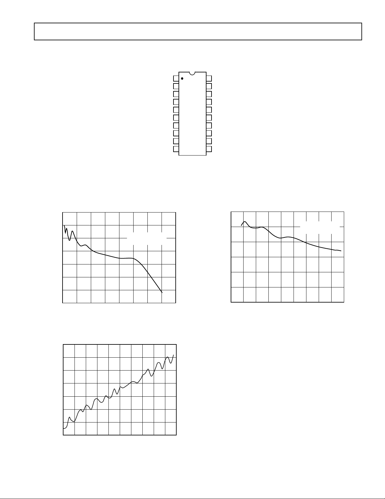
PIN CONFIGURATION
50Hz RIPPLE – V rms
120
0 0.080.01 0.02 0.03 0.04 0.05 0.06 0.07
100
60
40
20
0
80
AS PER DATA SHEET
CONDITIONS WITH
GAIN = 16
0.09
dBs
SOIC and DIP
AD7750
1
V
DD
2
G1
3
V
1+
V
4
1–
5
V
6
2+
V
7
2–
8
REFOUT
9
REFIN
10
DGND
Typical Performance Characteristics
140
120
AS PER DATA SHEET
CONDITIONS WITH
GAIN = 1
dBs
100
80
60
AD7750
TOP VIEW
(Not to Scale)
20
F1
19
F2
18
F
OUT
REVP
17
CLKOUTAGND
16
CLKIN
15
ACDC
14
S1
13
S2
12
FS
11
40
20
0
0 0.80.1 0.2 0.3 0.4 0.5 0.6 0.7
Figure 1. PSR as a Function of VDD 50 Hz Ripple
0.6
0.4
0.2
0
–0.2
Degrees
–0.4
–0.6
–0.8
45 5346 47 48 49 50 51 52
Figure 2. Phase Error as a Function of Line Frequency
50Hz RIPPLE – V rms
LINE FREQUENCY – Hz
Figure 3. PSR as a Function of VDD 50 Hz Ripple
54 55
–5–REV. 0

AD7750
V1 AMPLITUDE – mV rms
0.2
10
–2
–0.4
–0.6
0
10
–1
10
0
10
2
0.4
0.6
ERROR – % of Reading
V
DD
= 5.25V
V
DD
= 5.00V
V
DD
= 4.75V
–0.2
0.8
10
1
0.1
0.05
0
–0.05
–0.1
–0.15
ERROR – % of Reading
–0.2
–0.25
–0.3
0.001
0.01 0.1 1.0 10
V1 AMPLITUDE – mV rms
VDD = 5V
V2 = FULL SCALE
Figure 4. Error as a Percentage (%) of Reading Over a
Dynamic Range of 1000, Gain = 1
0
–0.05
–0.1
–0.15
–0.2
–0.25
–0.3
ERROR – % of Reading
–0.35
–0.4
–0.45
–0.5
0.0001
0.001
V1 AMPLITUDE – mV rms
VDD = 5V
V2 = FULL SCALE
0.01 0.1
0.6
0.4
V
= 5.25V
DD
0.2
0
V
= 5.00V
–0.2
ERROR – % of Reading
–0.4
–0.6
0
10
DD
V
= 4.75V
DD
1
10
V1 AMPLITUDE – mV rms
2
10
3
10
Figure 6. Measurement Error vs. Input Signal Level and
Varying V
with Channel 1, Gain = 1
DD
Figure 5. Error as a Percentage (%) of Reading Over a
Dynamic Range of 1000, Gain = 16
Figure 7. Measurement Error vs. Input Signal Level and
Varying V
–6– REV. 0
with Channel 1, Gain = 16
DD

AD7750
A CURRENT TRANSFORMER
PROVIDES COMPLEMENTARY
DIFFERENTIAL INPUTS TO THE
AD7750
A CURRENT SENSE RESISTOR
PROVIDES A SINGLE-ENDED
INPUT TO THE AD7750
V+
V–
V–
V+
SHUNT
RESISTOR
ANALOG INPUTS
The analog inputs of the AD7750 are high impedance bipolar
voltage inputs. The four voltage inputs make up two truly
differential voltage input channels called V
and V2. As with
1
any ADC, an antialiasing filter or low-pass filter is required on
the analog input. The AD7750 is designed with a unique
switched capacitor architecture that allows a bipolar analog
input with a single 5 V power supply. The four analog inputs
, V1–, V2+, V2–) each have a voltage range from –1.0 V to
(V
1+
+1.0 V. This is an absolute voltage range and is relative to the
ground (AGND) pin. This ground is nominally at a potential of
0 V relative to the board level ground. Figure 8 shows a very
simplified diagram of the analog input structure. When the analog input voltage is sampled, the switch is closed and a very
small sampling capacitor is charged up to the input voltage. The
resistor in the diagram can be thought of as a lumped component made up of the on resistance of various switches.
R
V
IN
1.4kV
2pF
C
SAMPLING
CAPACITOR
Figure 8. Equivalent Analog Input Circuit
Analog Inputs Protection Circuitry
The analog input section also has protection circuitry. Since the
power supply rails are 0 V to 5 V, the analog inputs can no
longer be clamped to the supply rails by diodes. Thus, the internal protection circuitry monitors the current paths during a fault
condition and protects the device from continuous overvoltage,
continuous undervoltage and ESD events. The maximum overvoltage the AD7750 analog inputs can withstand without causing irreversible damage is ±6 V relative to AGND pin.
In the case of continuous overvoltage and undervoltage the
series resistance of the antialiasing filter can be used to limit
input current. The total input current in the case of a fault
should be limited to 10 mA.
For normal operation of the AD7750 there are two further restrictions on the signal levels presented to the analog inputs.
1. The voltage on any input relative to the AGND pin must not
exceed ±1 V.
2. The differential voltage presented to the ADC (Analog
Modulator) must not exceed ±2 V.
In Figure 12, Channel 1 has a peak voltage on V
and V1– of
1+
±1 V. These signals are not gained (G1 = 0) and so the
differential signal presented to the modulator is ± 2 V.
However, Channel 2 has an associated gain of two and so
care must be taken to ensure the modulator input does not
exceed ±2 V. Therefore, the maximum signal voltage that
can appear on V
and V2– is ±0.5 V.
2+
The difference between single-ended and complementary
differential input schemes is shown in the diagram below,
Figure 9. For a single-ended input scheme the V– input is
held at the same potential as the AGND Pin. The maximum voltages can then be applied to the V+ input are
shown in Figures 10 and 11. An example of this input
scheme uses a shunt resistor to convert the line current to a
voltage that is then applied to the V
input of the AD7750.
1+
An example of the complementary differential input scheme
uses a current transformer to convert the line current to a
voltage that is then applied to V
and V1–. With this
1+
scheme the voltage on the V+ input is always equal to, but
of opposite polarity to the voltage on V–. The maximum
voltage that can be applied to the inputs of the AD7750
using this scheme is shown in Figures 12 and 13.
Note that the common mode of the analog inputs must
be driven. The output terminals of the CT are, therefore,
referenced to ground.
Figure 9. Examples of Complementary and SingleEnded Input Schemes
–7–REV. 0
AD7750
Figure 10. Maximum Input Signals with Respect to AGND for a Single-Ended Input Scheme, G1 = 0
V1+ = 61V MAX
= AGND
V
1–
V
= 61V MAX
2+
V2– = AGND
V1+ = 6125mV MAX
V
= AGND
1–
V
= 61V MAX
2+
V
= AGND
2–
61V MAX
ADC
ADC
ADC
ADC
DTF
DTF
F
OUT
F1
F2
F
OUT
F1
F2
X16
X2
61V
62V MAX
62V
62V MAX
62V
62V MAX
62V
X1
X2
Figure 11. Maximum Input Signals with Respect to AGND for a Single-Ended Input Scheme, G1 = 1
61V MAX
V+ = 61V MAX
ADC
ADC
DTF
F
OUT
F1
F2
V– = 61V MAX
V+ = 60.5V MAX
V– = 60.5V MAX
62V
X1
61V MAX
61V MAX
X2
62V
61V MAX
Figure 12. Maximum Input Signals for a Complementary Input Scheme, G1 = 0
61V MAX
V+ = 662.5V MAX
ADC
ADC
DTF
F
OUT
F1
F2
V– = 662.5V MAX
V+ = 60.5V MAX
V– = 60.5V MAX
X16
X2
62V
61V MAX
61V MAX
62V
61V MAX
Figure 13. Maximum Input Signals for a Complementary Input Scheme, G1 = 1
–8– REV. 0

AD7750
DETERMINING THE OUTPUT FREQUENCIES OF THE AD7750
F
, F1 and F2 are the frequency outputs of the AD7750. The
OUT
output frequencies of the AD7750 are a multiple of a binary
fraction of the master clock frequency CLKIN. This binary
fraction of the master clock is referred to as F
in this data
MAX
sheet. F
depending on which mode of operation the AD7750 is in. The
operating modes of the AD7750 are selected by the logic inputs
FS, S2 and S1. The table below outlines the F
and the transfer functions for the various operating modes of the
AD7750.
can have one of two values, F
MAX
Table I. Operating Mode
edoMSF2S1SnoitpircseDedoM2F,1F
0000 .edoMtnemerusaeMrewoP
1
)zH(F
F
1XAM
F.k±
1XAM
noitacilpitluMtnardnauQruoF
.)tuptuOedutingaMdnangiS(
1001 .edoMtnemerusaeMrewoP
F.kot0
1XAM
noitacilpitluMtnardnauQowT
.)ylnOedutingaM(
2010 .edoMtnemerusaeMrewoP
F.kot0
1XAM
noitacilpitluMtnardnauQowT
.)ylnOedutingaM(
2
3
011V
1
FnoedoMrotinoMlennahC
edoMtnemerusaeMrewoPFno1
,
.TUO
F
F.k±
1XAM
1XAM
.)tuptuOedutingaMdnangiS(2F
4100 .edoMtnemerusaeMrewoP
F
2XAM
F.k±
2XAM
noitacilpitluMtnardnauQruoF
.)tuptuOedutingaMdnangiS(
5101 .edoMtnemerusaeMrewoP
F.kot0
2XAM
noitacilpitluMtnardnauQowT
.)ylnOedutingaM(
6110 .edoMtnemerusaeMrewoP
F.kot0
2XAM
noitacilpitluMtnardnauQowT
.)ylnOedutingaM(
2
7
111V
2
FnoedoMrotinoMlennahC
F
.TUO
2XAM
F.k±
2XAM
,1FnoedoMtnemerusaeMrewoP
.)tuptuOedutingaMdnangiS(2F
NOTES
1
The variable k is proportional to the product of the rms differential input voltages on Channel 1 and Channel 2 (V
k = (1.32 × V1 × V2 × Gain)/V
2
Applies to F
ential voltage on Channel 2 (FS = 1, S1 = 1, S0 = 1), i.e., Channel Monitor Mode.
k = (0.81 × V)/V
V = V1 × Gain or
V = V2 × 2
NOTE: V1 and V2 here refer to the instantaneous differential voltage on Channel 1 or Channel 2, not the rms value.
only. The variable k is proportional to the instantaneous differential input voltage on Channel 1 (FS = 0, S1 = 1, S0 = 1) or the instantaneous differ-
OUT
REF
REF
2
1
TUO
F[.61
F[.23
F[.61
F[.61
and V2).
1
and F
MAX1
frequencies
MAX
)zH(F
F.k±
1XAM
F.kot0[.8
F.kot0[.61
1XAM
2XAM
F.kot0[.61
F.kot0[.23
2XAM
]F
1XAM
]F
1XAM
]F
1XAM
k±2F.
1XAM
F.k±
]F
2XAM
]F
2XAM
]F
2XAM
2
k±
F.
2XAM
F
F
F
]F
F
F
F
F
]F
F
XAM
1XAM
1XAM
1XAM
1XAM
1XAM
1XAM
1XAM
1XAM
2XAM
2XAM
2XAM
2XAM
2XAM
2XAM
2XAM
2XAM
MAX2
2/NIKLC=
zH8.6=
2/NIKLC=
zH8.6=
2/NIKLC=
zH8.6=
2/NIKLC=
zH8.6=
2/NIKLC=
zH6.31=
2/NIKLC=
zH6.31=
2/NIKLC=
zH6.31=
2/NIKLC=
zH6.31=
,
91
91
91
91
81
81
81
81
Mode Description (Table I)
The section of Table I labeled Mode Description summarizes
the functional modes of the AD7750. The AD7750 has two
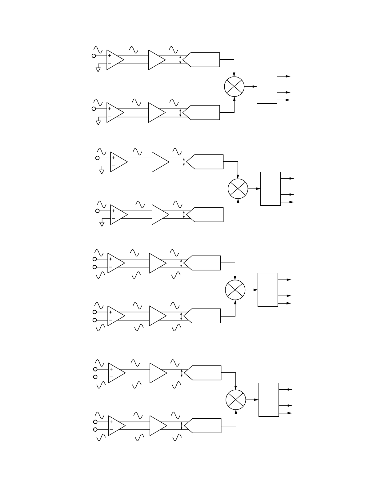
basic modes of operation, i.e., four and two quadrant multiplication. The diagram in Figure 14 is a graphical representation of
the transfer functions for two and four quadrant multiplication.
Four Quadrant Multiplication (Modes 0, 3, 4 and 7)
When the AD7750 is operating in its four quadrant multiplication mode the output pulse frequency on F1, F2 and F
OUT
contains both sign and magnitude information. The magnitude information is indicated by the output frequency variation
(k.F
) from a center frequency (F
MAX
). The sign informa-
MAX
tion is indicated by the sign of the frequency variation around
. For example if the output frequency is equal to F
F
MAX
then the magnitude of the product is given by k.F
k.F
MAX
MAX
MAX
–
and it has a negative sign.
Two Quadrant Multiplication (Modes 1, 2, 5 and 6)
When operating in this mode the output pulse frequency only
contains magnitude information. Again as in the case of four
–9–REV. 0
quadrant multiplication the magnitude information is included
in the output frequency variation (k.F
). However, in this
MAX
mode the zero power frequency is 0 Hz, so the output frequency
variation is from 0 Hz to (k.F
) Hz. Also note that a no-load
MAX
threshold and the reverse polarity indicator are implemented in
these modes see No Load Threshold and Reverse Polarity
Indicator sections. These modes are the most suitable for a
Class 1 meter implementation.
Channel Monitor Modes (Modes 3 and 7)
In this mode of operation the F
give product information. When FS = 0, the F
pulse frequency does not
OUT
output fre-
OUT
quency gives sign and magnitude information about the voltage on Channel 1. When FS = 1 the F
output frequency
OUT
gives sign and magnitude information about the voltage on
Channel 2.
Note the F1, F2 pulse outputs still continue to give power
information.

AD7750
FOUR QUADRANT MULTIPLICATION
(SIGN AND MAGNITUDE)
V2(+)
V2(–)
F
+ k 3 F
MAX
0
F
MAX
(+)
_ k 3 F
(–)
MAX
MAX
(1.32 3 V1 3 V2 3 GAIN)
K =
V
F
– k 3 F
MAX
V1(–) V1(+) V1(–) V1(+)
F
MAX
(–)
+ k 3 F
(+)
MAX
MAX
Figure 14. Transfer Functions (Four and Two Quadrant Multiplication)
Maximum Output Frequencies
Table II shows the maximum output frequencies of F
OUT
and
F1, F2 for the various operating modes of the AD7750. The
table shows the maximum output frequencies for dc and ac
input signals on V
applied to V
and V2. When an ac signal (sinusoidal) is
1
and V2 the AD7750 produces an output frequency
1
which is proportional to the product of the rms value of these
inputs. If two ac signals with peak differential values of V
and V
the output frequency is proportional to V
sqrt(2) = (V
are applied to Channels 1 and 2, respectively, then
2MAX
1MAX
× V
2MAX
)/2. If V
1MAX
1MAX
and V
/sqrt(2) × V
2MAX
1MAX
2MAX
are also the
/
maximum dc input voltages then the maximum output frequencies for ac signals will always be half that of dc input signals.
Example calculation of F1, F2 max for Mode 2 and Gain = 1.
The maximum input voltage (dc) on Channel 1 is 2 V (V
+1 V, V
= –1 V)—see Analog Inputs section. The maximum
1–
=
1+
input voltage on Channel 2 is 1 V. Using the transfer function:
k = (1.32 × V
× V2 × Gain)/V
1
REF
2
k = 0.4224
F1, F2 = k.6.8 Hz = 2.9 Hz
FUNCTIONAL DESCRIPTION
The AD7750 combines two analog-to-digital converters, a digital multiplier, digital filters and a digital-to-frequency (DTF)
converter onto one low cost integrated circuit. The AD7750 is
fabricated on a double poly CMOS process (0.6 µ) and retains
its high accuracy by performing all multiplications and manipulations in the digital domain. The schematic in Figure 15 shows
an equivalent circuit for the AD7750 signal processing chain.
The first thing to notice is that the analog signals are first converted to digital signals by the two second-order sigma-delta
modulators. All subsequent signal processing is carried out in
the digital domain. The main source of errors in an application
is therefore in the analog-to-digital conversion process. For this
TWO QUADRANT MULTIPLICATION
( MAGNITUDE ONLY)
V2(+)
V2(–)
k
3 F
MAX
(+)
k
3 F
MAX
(+)
REF
k 3 F
MAX
(+)
3 F
k
MAX
(+)
2
reason great care must be taken when interfacing the analog
inputs of the AD7750 to the transducer. This is discussed in the
Applications section.
HPF in Channel 1
To remove any dc offset that may be present at the output
modulator 1, a user selectable high-pass IIR filter (Pin ACDC)
can be introduced into the signal path. This HPF is necessary
when carrying out power measurements. However, this HPF
has an associated phase lead given by 90°–tan
–1
(f/2.25). Figure
16 shows the transfer function of the HPF in Channel 1. The
Phase lead is 2.58° at 50 Hz. In order to equalize the phase
difference between the two channels a fixed time delay is introduced. The time delay is set at 143 µs, which is equivalent to a
phase lag of –2.58° at 50 Hz. Thus the cumulative phase shift
through Channel 1 is 0°.
Because the time delay is fixed, external phase compensation
circuitry will be required if the line frequency differs from
50 Hz. For example with a line frequency of 60 Hz the phase
lead due to the HPF is 2.148° and the phase lag due to the fixed
time delay is 3.1°. This means there is a net phase lag in Channel 1 of 0.952°. This phase lag in Channel 1 can be compensated for by using a phase lag compensation circuit like the
one shown in Figure 17. The phase lag compensation is placed
on Channel 2 (voltage channel) to equalize the channels. The
antialiasing filter associated with Channel 1 (see Applications
section) produces a phase lag of 0.6° at 50 Hz; therefore, to
equalize the channels, a net phase lag of (0.6° + 0.952°) 1.552°
should be in place on Channel 2. The gain trim resistor VR1
(100 Ω) produces a phase lag variation of 1.4° to 1.5° with VR2
= 0 Ω. VR2 can add an additional 0.1° phase lag (VR2 = 200 Ω).
–10– REV. 0
AD7750
Table II. Maximum Output Frequencies
)zH(2F,1F
F
edoMSF2S1S
)CD(
0000 9.2±8.664±90154.1±8.632±901
1001 9.2ot032ot054.1ot05.11ot0
2010 9.2ot064ot054.1ot032ot0
3011 9.2±8.6241±81254.1±8.6241±812
4100 8.5±6.3129±8129.2±6.3164±812
5101 8.5ot029ot09.2ot064ot0
6110 8.5ot0481ot09.2ot029ot0
7111 8.5±6.31241±8129.2±6.31241±812
TUO
)zH(
)CD(
)zH(2F,1F
F
)CA(
TUO
)zH(
)CA(
ADC 1
ADC 2
ACDC
HPF
PHASE LEAD OF
2.588C AT 50Hz
G1
V
1+
V
1–
V
2+
V
2–
PGA
X2
Figure 15. Equivalent AD7750 Signal Processing Chain
sRC
H(s) =
1 + sRC
C
R
R = 1MV
C = 0.0707mF
Figure 16. HPF in Channel 1
R1
1MV
VR1
100V
R3
860:1 ATTENUTATION
1.1kV
47nF
33kV
VR2
200V
C1
R2
33nF
R4
1.1kV
33mF
C2
C3
PIN 7
PIN 6
Figure 17. Phase Lag Compensation on Channel 1 for
60 Hz Line Frequency
TIME DELAY 143ms
(CLKIN = 3.5795MHz)
2.588C AT 50Hz
DIGITAL-TO-FREQUENCY BLOCK
COUNTER/ACCUMULATOR
τ
DIGITAL
MULTIPLIER
LPF
CLKIN
F
OUT
DTF
FS
S2 S1
F1
F2
Digital-to-Frequency Converter (DTF)
After they have been filtered, the outputs of the two sigma-delta
modulators are fed into a digital multiplier. The output of the
multiplier is then low-pass filtered to obtain the real power
information. The output of the LPF enters a digital-to-frequency
converter whose output frequency is now proportional to the
real power. The DTF offers a range of output frequencies to
suit most power measurement applications. There is also a high
frequency output called F
, which can be used for calibra-
OUT
tion purposes. The output frequencies are determined by the
logic inputs FS, S2 and S1. This is explained in the section of
this data sheet called Determining the Output Frequencies of
the AD7750.
Figure 18 shows the waveforms of the various frequency outputs. The outputs F1 and F2 are the low frequency outputs
that can be used to directly drive a stepper motor or electromechanical pulse counter. The F1 and F2 outputs provide two
alternating low going pulses. The pulsewidth is set at 275 ms
and the time between the falling edges of F1 and F2 is approximately half the period of F1. If, however, the period of
F1 and F2 falls below 550 ms (1.81 Hz) the pulsewidth of F1
and F2 is set to half the period. For example in Mode 3,
where F1 and F2 vary around 6.8 Hz, the pulsewidth would vary
from 1/2.(6.8+1.45) seconds to 1/2.(6.8–1.45) seconds—see
Table II.
–11–REV. 0

AD7750
The high frequency F
communications (via IR LED) and calibration purposes. F
output is intended to be used for
OUT
OUT
produces a 90 ms wide pulse at a frequency that is proportional
to the product of Channel 1 and Channel 2 or the instantaneous voltage on Channel 1 or Channel 2. The output frequencies are given in Table I in the Determining the Output
Frequencies of the AD7750 section of this data sheet. As in
the case o f F1 and F2, if the period of F
the F
F
F
pulsewidth is set to half the period. For example, if the
OUT
frequency is 20 Hz, the F
OUT
F1
F2
OUT
t
1
t
6
t
3
t
4
t
5
OUT
t
2
falls below 180 ms,
OUT
pulsewidth is 25 ms.
V
DD
0V
V
DD
0V
V
DD
0V
Figure 18. Timing Diagram for Frequency Outputs
VOLTAGE REFERENCE
The AD7750 has an on-chip temperature compensated bandgap voltage reference of 2.5 V with a tolerance of ±250 mV.
The temperature drift for the reference is specified at 50 ppm/°C.
It should be noted that this reference variation will cause a
frequency output variation from device to device for a given set
of input signals. This should not be a problem in most applications since it is a straight gain error that can easily be removed
at the calibration stage.
meter accuracy with small load currents. Hence an error of less
than 1% from 4% Ib to 400% Ib will be easier to achieve.
We will assume the design of a Class 1 meter. The specification
(IEC1036) requires that the meter have an error of no greater
than 1% over the range 4% Ib to 400% Ib (I
the basic current
1
. In addition, we will design a meter that ac-
), where Ib is
MAX
commodates signals with a crest factor of 2. The crest factor is
the ratio of V
/V rms. A pure sinusoidal waveform has a crest
PEAK
of sqrt(2) = 1.414 and an undistorted triangular waveform has a
crest factor of sqrt(3) = 1.73. Using a gain of 1 on Channel 1
the maximum differential signal which can be applied to Channel 1 is ±2 V—See Analog Input Ranges section. With a crest
factor of 2 the maximum rms signal on Channel 1 is, therefore,
1 V rms (equivalent to I
). The smallest signal (4% Ib) ap-
MAX
pearing on Channel 1 is therefore 10 mV rms.
Load Current Channel 1
4% Ib 10 mV rms
Ib 250 mV rms
400 Ib 1 V rms
2
400% Ib
0. 2
0. 02
4% Ib
CHANNEL 1 INPUT SIGNAL – Vrms
1
0.01
REVERSE POLARITY INDICATOR
When the AD7750 is operated in a Magnitude Only mode of
operation (i.e., Modes 1, 2, 5 and 6), and the polarity of the
power changes, the logic output REVP will go high. However,
the REVP pin is only activated when the there is pulse output
on F1 or F2. Therefore, if the power being measured is low, it may
be some time before the REVP pin goes logic high even though the
polarity of the power is reversed. Once activated the REVP output
will remain high until the AD7750 is powered down.
APPLICATIONS INFORMATION
Designing a Single Phase Class 1 Energy Meter (IEC 1036)
The AD7750 Product-to-Frequency Converter is designed for
use in a wide range of power metering applications. In a typical
power meter two parameters are measured (i.e., line voltage and
current) and their product obtained. The real power is then
obtained by low-pass filtering this product result. The line
voltage can b e measured through a resistor divider or voltage
transformer, and the current can be sensed and converted to
a voltage through a shunt resistor, current transformer or hall
effect device.
The design methodology used in the following example is to use
the upper end of the current channel dynamic range, i.e., Channel 1 of the AD7750. The assumption here is that the signal on
the voltage channel will remain relatively constant while the
signal on the current channel will vary with load. Using the
upper end of the dynamic range of Channel 1 will improve the
1
See IEC 1036 2nd Edition 1996-09 Section 3.5.1.1.
–12– REV. 0
0. 002
Figure 19. Use the Upper End of the Dynamic Range of
Channel 1 (Current)
Calculations for a 100 PPKWHR Meter
The AD7750 offers a range of maximum output frequencies—
see Table I and Table II. In the Magnitude Only modes of
operation the two maximum output frequencies are 1.45 Hz
and 2.9 Hz. The signal on the voltage channel (Channel 2) is
scaled to achieve the correct output pulse frequency for a given
load (e.g., 100 PPKWHR). The relationship between the input
signals and the output frequency is given by the equation:
Freq = k × F
where k = (1.32 × V1 × V2 × Gain)/V
F
= 6.8 Hz or 13.6 Hz depending on the mode—see Table
MAX
I, Gain is the gain of Channel 1, V
voltages on Channels 1 and 2 and V
MAX
and V2 are the differential
1
is the reference voltage
REF
REF
2
(2.5 V ± 8%).
To design a 100 PPKWHR meter with Ib = 15 A rms and a line
voltage of 220 V rms the output pulse frequency with a load
current of Ib is 0.0916 Hz (See Calculation 1 below).
Therefore, 0.0916 Hz = k × 6.8 Hz (Mode 2) or k = 0.01347.
With a load current of Ib the signal on Channel 1 (V
) is equal
1
to 0.25 V rms (remember 400% Ib = 1 V rms) and, therefore,
the signal on Channel 2 (V
) is equal to 0.255 V rms (See Calcula-
2
tion 2). This means that the nominal line voltage (220 V rms)
needs to be attenuated by approximately 860, i.e., 220/0.255.

AD7750
TIME 2 ms
5.065
5.060
5.050
600 620
VOLTS
5.055
640 660 680 700 720 740 760 780 800
For 100 PPKWHR V2 is equal to 0.255 V rms or the line voltage attenuated by a factor of 860.
Calculation 1
100 PPKWHR = 0.02777 Hz/kW.
Ib of 15 A rms and line voltage of 220 V = 3.3 kΩ. Hence, the
output frequency is given by 3.3 × 0.02777 Hz = 0.0916 Hz.
Calculation 2
k = (1.32 × V
0.01347 = (1.32 × 0.25 × V
= 0.255.
V
2
× V2 × Gain)/V
1
2
.
REF
× 1)/6.25.
2
Figure 21 below shows how the design equations from the previous page are implemented.
Measuring the Load Current
The load current is converted to a voltage signal for Channel 1
using a CT (Current Transformer). A 15 A rms load should
produce a 250 mV rms signal on Channel 1. A CT with a turns
ratio of 120 and a shunt resistor of 2 Ω. will carry out the necessary current to voltage conversion. The CT and its shunt resistance should be placed as close as possible to the AD7750. This
will improve the accuracy of the meter at very small load currents. At small load currents the voltage levels on Channel 1 are
in the order of 10 mV and the meter is more prone to error due
to stray signal “pick up.” When measuring power the HPF in
the current channel must be switched on. This is done by connecting the ACDC pin to V
NOTE: The voltage signals on V
.
DD
and V1– must be referenced
1+
to ground. This can be achieved as shown in Figure 21 below,
i.e., by referencing 1/2 R
to ground or by connecting a
CT
centertap on the CT secondary to ground.
Measuring the Line Voltage
When the AD7750 is biased around the live wire as shown in
Figure 21, the task of measuring the line voltage is greatly
simplified. A resistor divider attenuates the line voltage and
provides a single-ended input for Channel 2. The component
values of the divider are chosen to give the correct rating (e.g.,
100 PPKWHR) for the meter. See the design equations on the
previous page. For this design an attenuation ratio of 860:1 is
required.
V
DD
C5
C7
C11
Z1
C8
R7
C10
C12
V
DD
LOAD
PHASE
NEUTRAL
SOURCE
*BIASING AROUND THE LIVE WIRE PATENTED BY SCHLUMBERGER.
CT
120:1
MOV
1/2 R
1/2 R
R5
*
C1
R1
CT
1V
CT
1V
VR1
R6
R4
C6
R3
C9
D1
D2
R2
C2
Antialiasing Components Channels 1 and 2
The AD7750 is basically two ADCs and a digital multiplier. As
with any ADC, a LPF (Low-Pass Filter) should be used on the
analog inputs to avoid out of band signal being aliased into the
band of interest. In the case of a Class 1 meter the band of
interest lies in the range 48 Hz to 1 kHz approximately. The
components R3, R4, R6, R7, C5, C6, C9 and C10 make up the
LPFs on each of the four analog inputs. Note that although
Channel 2 is used single ended a LPF is still required on V
.
2–
Power Supply Circuit
The AD7750 operates from a single power supply of 5 V ± 5%
but still accommodates input signals in the range ±1 V. Because
the AD7750 doesn’t require dual supplies the number of external components for the power supply is reduced. One of the
most important design goals for the power supply is to ensure
that the ripple on the output is as low as possible. Every analog
or mixed signal IC is to a greater or lesser extent susceptible to
power supply variations. Power supply variations or ripple, if
large enough, may affect the accuracy of the device when measuring small signals. The plot in Figure 20 shows the ripple
associated with the circuit in Figure 21. The ripple is in the
region of 10 mV peak to peak.
Figure 20. Power Supply Ripple
1
2
3
4
5
AD7750
TOP VIEW
6
(Not to Scale)
7
8
9
10
20
M
19
18
17
16
15
14
13
12
11
PULSE COUNTER
R8
R9
C4
C3
V
DD
V
DD
D5
D4
D3
REVERSE POLARITY
INDICATOR
XTAL 3.57954MHz
MODE2
IR DIODE FOR
CALIBRATION
Figure 21. Suggested Class 1 Meter Implementation
–13–REV. 0

AD7750
Registering the Power Output
The low frequency pulse outputs (F1 and F2) of the AD7750
provide the frequency output from the product-to-frequency
conversion. These outputs can be used to drive a stepper motor
or impulse counter.
A high frequency output is available at the pin F
. This high
OUT
frequency output is used for calibration purposes. In Mode 2
the output frequency is 16 × F1(2). With a load current of Ib
the frequency at F
will be 1.4656 Hz (0.0916 Hz × 16 from
OUT
calculations). If a higher frequency output is required, the FS
pin can be set to V
5 V for calibration. In this case the output
DD
frequency is equal to 64 × F1 or 5.8624 Hz at Ib—see Table I.
NO LOAD THRESHOLD OF THE AD7750
The AD7750 will detect when the power drops below a certain
level. When the power (current) drops below a predefined
threshold the AD7750 will cease to generate an output drive for
the stepper motor (F1, F2). This feature of the AD7750 is
intended to reproduce the behavior of Ferraris meters. A
Ferraris meter will have friction associated with the wheel rotation, therefore the wheel will not rotate below a certain power
level. The no load threshold is only implemented in the Magnitude Only modes (Modes 1, 2, 5 and 6—see Table I). The
IEC1036 specification includes a test for this effect by requiring
no output pulses during some predetermined time period. This
time period is calculated as:
time period = 60,000/pulses-per-minute
If a meter is calibrated to 100 PPKWHR with a F
OUT
running
16 times faster than F1 and F2, this time period is 37.5 minutes
(60,000/1,600). The IEC1036 specifications state that the no
load threshold must be less than the start up current level. This
is specified as 0.4% of Ib.
The threshold level for a given design can be easily calculated
given that the minimum output frequency of the AD7750 is
0.00048% of the maximum output frequency for a full-scale
differential dc input. For example if FS = 0, the maximum
output frequency for a full-scale dc input is 2.9 Hz (see Table II)
and the minimum output frequency is, therefore, 1.39 × 10
Calculating the Threshold Power (Current)
–5
Hz.
The meter used in this example is calibrated to 100 PPKWHR,
has an Ib (basic current) of 15 A rms, the line voltage is 220 V
rms and the turns ratio of the CT on Channel 1 is 120:1 with an
2 Ω shunt resistor.
The nominal voltage on Channel 2 of the AD7750 is 255 mV
rms. An F
of 6.8 Hz is selected by setting FS = 0. A Magni-
MAX
tude Only Mode (Mode 2) is selected to enable the no load threshold. The gain on Channel 1 is set to 1. The threshold power or
current can be found by using the transfer function in Table I.
F1, F2 = (1.32
×
V1 × V2 × Gain × F
MAX
)/V
REF
2
From the transfer function V1 is calculated as 37.95 µV rms—
see Calculation 3.
This is equivalent to a line current of:
(37.95 µV/2 Ω ) × 120 = 2.27 mA rms or 0.5 W
or
×
(2.27 mA/15 A)
100% = 0.015% of Ib.
NOTE: The no load threshold as a percentage of Ib will be
different for each value of Ib since the no load in watts is fixed:
FS = 0, the no load threshold is (F
= 6.8 Hz)
MAX
0.5 Watts for a 100 PPKWHR meter
5 Watts for a 10 PPKWHR meter
FS = 1, the no load threshold is (F
= 13.6 Hz)
MAX
1 Watt for a 100 PPKWHR meter
10 Watts for a 10 PPKWHR meter
Calculation 3
F
= 1.32 × V1 × V2 × Gain × 6.8 Hz) V
MIN
REF
2
1.39 × 10⁻⁵ Hz = V1 × 0.2555 × 1 × 6.8)/6.25
= 37.95 µV
V
1
EXTERNAL LEAD/LAG COMPENSATION
External phase compensation is often required in a power meter
design to eliminate the phase errors introduced by transducers
and external components. The design restriction on any external
compensating network is that the network must have an overall
low-pass response with a 3 dB point located somewhere between
5 kHz and 6 kHz. The corner frequency of this LPF(s) is much
higher than the band of interest. The reason for this is to minimize its effect on phase variation at 50 Hz due to component
tolerances.
With the antialiasing filters on all channels having the same
corner (–3 dB) frequency, the main contribution to phase error
will be due to the CT. A phase lead in a channel is compensated
by lowering the corner frequency of the antialiasing filter to
increase its associated lag and therefore cancel the lead. A phase
lag in a channel should be compensated by introducing extra lag
in the other channel. This can be done as previously described,
i.e., moving the corner frequency of the antialiasing filters. The
result in this case is that the signal on both channels has the
same amount of phase lag and is therefore in phase at the analog
inputs to the AD7750. The recommended RC values for the
antialiasing filters on the voltage and current channels (see
Antialiasing Components Channels 1 and 2) are R = 1 kΩ,
C = 33 nF and R = 100 Ω, C = 330 nF respectively. These
values produce a phase lag of 0.6° through the filters. Varying R
in the antialiasing network from 80 Ω to 100 Ω or 800 Ω to 1 kΩ
produces a phase variation from 0.475° to 0.6° at 50 Hz. This
allows the user to vary the lag by 0.125°.
–14– REV. 0

AD7750
Table III. Components for Suggested Class 1 Meter Implementation in Figure 21
Schematic
Designator Description Comments
R1 470 Ω, 5%, 1 W
R2 1 kΩ , 5%, 1/2 W
R3, R4, 100 Ω, 10%, 1/2W These registers are required to form part of the antialiasing filtering on the analog inputs;
R7 1 kΩ, 10%, 1/2 W they do not perform a voltage-to-current conversion.
R5 1 MΩ , 5%, 2 W The choice of R5 determines the attenuation on the voltage channels and hence the meter
rating, e.g., 100 PPKWHR.
R6 1.1 kΩ, 5%, 1/2 W Forms part of the Gain Calibration network with R5 and VR1.
R8, R9 500 Ω, 10%, 1/2 W
VR1 100 Ω, 10/15 Turn This potentiometer is used to perform the Gain Calibration of the meter. Attenuation of
830 to 900—see Applications section.
C1 470 nF, 250 V ac
C2 100 µF, 24 V dc
C3, C4 33 pF
C5, C6, 330 nF Forms part of the antialiasing filters on the analog inputs.
C9, C10 33 nF
C7, C11 10 µF, 10 V
C8, C12 10 nF
Z1 1N750
D1, D2 1N4007
D3 LED
D4, D5 IR LEDS
XTAL 3.579545 MHz
MOV V250PA40A Metal Oxide Varistor–Harris Semiconductor.
–15–REV. 0

AD7750
0.210 (5.33)
MAX
0.160 (4.06)
0.115 (2.93)
OUTLINE DIMENSIONS
Dimensions shown in inches and (mm).
20-Lead Plastic DIP
(N-20)
1.060 (26.90)
0.925 (23.50)
20
110
PIN 1
0.022 (0.558)
0.014 (0.356)
0.100
(2.54)
BSC
11
0.070 (1.77)
0.045 (1.15)
0.280 (7.11)
0.240 (6.10)
0.060 (1.52)
0.015 (0.38)
0.130
(3.30)
MIN
SEATING
PLANE
0.325 (8.25)
0.300 (7.62)
20-Lead Wide Body SOIC
(R-20)
0.5118 (13.00)
0.4961 (12.60)
0.195 (4.95)
0.115 (2.93)
0.015 (0.381)
0.008 (0.204)
C3156–8–10/97
20 11
PIN 1
0.0118 (0.30)
0.0040 (0.10)
0.0500
(1.27)
BSC
0.1043 (2.65)
0.0926 (2.35)
0.0192 (0.49)
0.0138 (0.35)
101
SEATING
PLANE
0.2992 (7.60)
0.2914 (7.40)
0.4193 (10.65)
0.3937 (10.00)
0.0125 (0.32)
0.0091 (0.23)
0.0291 (0.74)
0.0098 (0.25)
0.0500 (1.27)
8°
0°
0.0157 (0.40)
x 45°
–16–
PRINTED IN U.S.A.
REV. 0
 Loading...