Analog Devices AD7750 Datasheet

Product-to-Frequency
DELAY
2.5V
BAND GAP
REFERENCE
DTF
HPF
MULT
S1FS
VDD
DGND
DTF
LPF
2ND ORDER
MODULATOR
AGND REFOUT
G1
ADC1
ADC2
REFIN
V
1+
AD7750
2ND ORDER
MODULATOR
x2
x16
V
2+
S2
V
1–
V
2–
F2
CLKOUT
F1
F
OUT
REVP
CLKIN
ACDC
a
FEATURES
Two Differential Analog Input Channels
Product of Two Channels
Voltage-to-Frequency Conversion on a Single Channel
Real Power Measurement Capability
< 0.2% Error Over the Range 400% Ibasic to 2% Ibasic
Two or Four Quadrant Operation (Positive and
Negative Power)
Gain Select of 1 or 16 on the Current Channel (Channel 1)
Choice of On-Chip or External Reference
Choice of Output Pulse Frequencies Available
(Pins F1 and F2)
High Frequency Pulse Output for Calibration Purposes
(F
)
OUT
HPF on Current Channel for Offset Removal
Single 5 V Supply and Low Power
Converter
AD7750
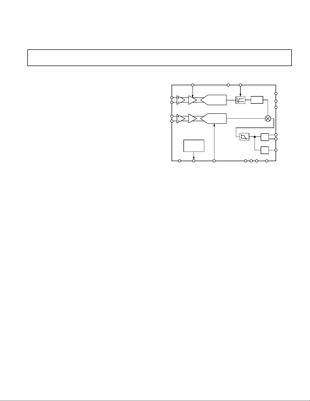
FUNCTIONAL BLOCK DIAGRAM
GENERAL DESCRIPTION
The AD7750 is a Product-to-Frequency Converter (PFC)
that can be configured for power measurement or voltage-tofrequency conversion. The part contains the equivalent of two
channels of A/D conversion, a multiplier, a digital-to-frequency
converter, a reference and other conditioning circuitry. Channel 1
has a differential gain amplifier with selectable gains of 1 or 16.
Channel 2 has a differential gain amplifier with a gain of 2. A highpass filter can be switched into the signal path of Channel 1 to
remove any offsets.
The outputs F1 and F2 are fixed width (275 ms) logic low going
pulse streams for output frequencies less than 1.8 Hz. A range
of output frequencies is available and the frequency of F1 and
F2 is proportional to the product of V
and V2. These outputs
1
PRODUCT HIGHLIGHTS
1. The part can be configured for power measurement or
voltage-to-frequency conversion.
2. The output format and maximum frequency is selectable;
from low-frequency outputs, suitable for driving stepper
motors, to higher frequency outputs, suitable for calibration
and test.
3. There is a reverse polarity indicator output that becomes
active when negative power is detected in the Magnitude
Only Mode.
4. Error as a % of reading over a dynamic range of 1000:1 is
< 0.3%.
are suitable for directly driving an electromechanical pulse
counter or full stepping two phase stepper motors. The outputs
can be configured to represent the result of four-quadrant multiplication (i.e., Sign and Magnitude) or to represent the result of
a two quadrant multiplication (i.e., Magnitude Only). In this
configuration the outputs are always positive regardless of the
input polarities. In addition, there is a reverse polarity indicator
output that becomes active when negative power is detected in
the Magnitude Only Mode, see Reverse Polarity Indicator.
The error as a percent (%) of reading is less than 0.3% over a
dynamic range of 1000:1.
The AD7750 is fabricated on 0.6 µ CMOS technology; a pro-
cess that combines low power and low cost.
REV. 0
Information furnished by Analog Devices is believed to be accurate and
reliable. However, no responsibility is assumed by Analog Devices for its
use, nor for any infringements of patents or other rights of third parties
which may result from its use. No license is granted by implication or
otherwise under any patent or patent rights of Analog Devices.
One Technology Way, P.O. Box 9106, Norwood, MA 02062-9106, U.S.A.
Tel: 781/329-4700 World Wide Web Site: http://www.analog.com
Fax: 781/326-8703 © Analog Devices, Inc., 1997

(VDD = 5 V 6 5%, AGND = 0 V, DGND = 0 V, REFIN = +2.5 V, CLKIN = 3.58 MHz
T
to T
AD7750–SPECIFICA TIONS
MIN
A Version
–408C to
Parameter +858C Units Test Conditions/Comments
ACCURACY
Measurement Error
1
Gain = 1 0.2 % Reading max Measured Over a Dynamic Range on Channel 1 of 500:1
0.3 % Reading max Measured Over a Dynamic Range on Channel 1 of 1000:1
Gain = 16 0.2 % Reading max Measured Over a Dynamic Range on Channel 1 of 500:1
0.4 % Reading max Measured Over a Dynamic Range on Channel 1 of 1000:1
Phase Error Between Channels CLKIN = 3.58 MHz, Line Frequency = 50 Hz
Phase Lead 40° (PF = +0.8) ±0.2 Degrees (°) max HPF Filter On, ACDC = 1
Phase Lag 60° (PF = –0.5) ±0.2 Degrees (°) max HPF Filter On, ACDC = 1
Feedthrough Between Channels HPF Filter On, ACDC = 1, Mode 3, Channel 1 = 0 V
Output Frequency Variation (F
) 0.0005 % Full-Scale max Channel 2 = 500 mV rms at 50 Hz
OUT
Power Supply Rejection HPF Filter On, ACDC = 1, Mode 3, Channel 1 = 0 V
Output Frequency Variation (F
) 0.03 % Full-Scale max Channel 2 = 500 mV rms, Power Supply Ripple
OUT
ANALOG INPUTS
Maximum Signal Levels ±1 V max On Any Input, V1+, V1–, V2+ and V2–. See Analog Inputs.
Input Impedance (DC) 400 kΩ min CLKIN = 3.58 MHz
Bandwidth 3.5 kHz typ CLKIN = 3.58 MHz, CLKIN/1024
Offset Error ±10 mV typ
Gain Error ±4 % Full-Scale typ
Gain Error Match ±0.3 % Full-Scale typ
REFERENCE INPUT
REF
Input Voltage Range 2.7 V max 2.5 V + 8%
IN
2.3 V min 2.5 V – 8%
Input Impedance 50 kΩ min
ON-CHIP REFERENCE Nominal 2.5 V
Reference Error ±200 mV max
Temperature Coefficient 55 ppm/°C typ
CLKIN
Input Clock Frequency 4.5 MHz max
2 MHz min
LOGIC INPUTS
FS, S1, S2, ACDC and G1
Input High Voltage, V
Input Low Voltage, V
Input Current, I
Input Capacitance, C
INL
IN
IN
INH
2.4 V min VDD = 5 V ± 5%
0.8 V max VDD = 5 V ± 5%
±10 µA max Typically 10 nA, VIN = 0 V to V
10 pF max
CLKIN
Input High Voltage, V
Input Low Voltage, V
LOGIC OUTPUTS
INH
INL
2
4 V min
0.4 V max
F1 and F2
Output High Voltage, V
OH
4.3 V min V
Output Low Voltage, V
OL
0.5 V max V
F
and REVP
OUT
Output High Voltage, V
OH
4 V min V
Output Low Voltage, V
OL
0.4 V max V
High Impedance Leakage Current ±10 µA max
High Impedance Capacitance 15 pF max
= –408C to +858C, ACDC = Logic High)
MAX
Channel 2 with Full-Scale Signal
250 mV at 50 Hz. See Figures 1 and 3.
I
= 8 mA
SOURCE
= 5 V
DD
I
= 8 mA
SINK
= 5 V
DD
I
= 1 mA
SOURCE
= 5 V ± 5%
DD
I
= 200 µA
SINK
= 5 V ± 5%
DD
DD
–2– REV. 0

AD7750
WARNING!
ESD SENSITIVE DEVICE
A Version
–408C to
Parameter +858C Units Test Conditions/Comments
POWER SUPPLY For Specified Performance, Digital Input @ AGND
or V
V
DD
4.75 V min 5 V – 5%
5.25 V max 5 V + 5%
I
DD
NOTES
1
See plots in Typical Performance Graphs.
2
External current amplification/drive should be used if higher current source and sink capabilities are required, e.g., bipolar transistor.
All specifications subject to change without notice.
5.5 mA max Typically 3.5 mA
DD
(VDD = 5 V, AGND = 0 V, DVDD = 0 V, REFIN = REFOUT. All specifications T
TIMING CHARACTERISTICS
1, 2
unless otherwise noted.)
Parameter A Version Units Test Conditions/Comments
3
t
1
t
2
t
3
3
t
4
t
5
t
6
NOTES
1
Sample tested during initial release and after any redesign or process change that may affect this parameter.
2
See Figure 18.
3
The pulsewidths of F1, F2 and F
Specifications subject to change without notice.
ABSOLUTE MAXIMUM RATINGS*
(TA = +25°C unless otherwise noted)
VDD to AGND . . . . . . . . . . . . . . . . . . . . . . . . . –0.3 V to +7 V
to DGND . . . . . . . . . . . . . . . . . . . . . . . . . –0.3 V to +7 V
V
DD
Analog Input Voltage to AGND
, V1–, V2+ and V2– . . . . . . . . . . . . . . . . . . . . –6 V to +6 V
V
1+
Reference Input Voltage to AGND . . . . –0.3 V to V
Digital Input Voltage to DGND . . . . . . –0.3 V to V
Digital Output Voltage to DGND . . . . . –0.3 V to V
Operating Temperature Range
Commercial (A Version) . . . . . . . . . . . . . . .–40°C to +85°C
Storage Temperature Range . . . . . . . . . . . . –65°C to +150°C
Junction Temperature . . . . . . . . . . . . . . . . . . . . . . . . . +150°C
275 ms F1 and F2 Pulsewidth (Logic Low)
See Table I s Output Pulse Period. See Table I to Determine the Output Frequency
t2/2 s Time Between F1 Falling Edge and F2 Falling Edge
90 ms F
See Table I s F
Pulsewidth (Logic High)
OUT
Pulse Period. See Table I to Determine the Output Frequency
OUT
CLKIN/4 s Minimum Time Between F1 and F2 Pulse
are not fixed for higher output frequencies. See the Digital-to-Frequency Converter (DTF) section for an explanation.
OUT
20-Lead SOIC Package, Power Dissipation . . . . . . . . 450 mW
Thermal Impedance . . . . . . . . . . . . . . . . . . . . . 74°C/W
θ
JA
Lead Temperature, Soldering
Vapor Phase (60 sec) . . . . . . . . . . . . . . . . . . . . . +215°C
Infrared (15 sec) . . . . . . . . . . . . . . . . . . . . . . . . . +220°C
20-Lead Plastic DIP, Power Dissipation . . . . . . . . . . 450 mW
Thermal Impedance . . . . . . . . . . . . . . . . . . . . 102°C/W
θ
+ 0.3 V
DD
+ 0.3 V
DD
+ 0.3 V
DD
JA
Lead Temperature, Soldering
Vapor Phase (60 sec) . . . . . . . . . . . . . . . . . . . . . +215°C
Infrared (15 sec) . . . . . . . . . . . . . . . . . . . . . . . . . +220°C
*Stresses above those listed under Absolute Maximum Ratings may cause perma-
nent damage to the device. This is a stress rating only; functional operation of the
device at these or any other conditions above those listed in the operational
sections of this specification is not implied. Exposure to absolute maximum rating
conditions for extended periods may affect device reliability.
MIN
to T
MAX
ORDERING GUIDE
Temperature Package Package
Model Range Description Options
AD7750AN –40°C to +85°C 20-Lead Plastic DIP N-20
AD7750AR –40°C to +85°C 20-Lead Wide Body SOIC R-20
CAUTION
ESD (electrostatic discharge) sensitive device. Electrostatic charges as high as 4000 V readily
accumulate on the human body and test equipment and can discharge without detection.
Although the AD7750 features proprietary ESD protection circuitry, permanent damage may
occur on devices subjected to high energy electrostatic discharges. Therefore, proper ESD
precautions are recommended to avoid performance degradation or loss of functionality.
–3–REV. 0

AD7750
PIN FUNCTION DESCRIPTIONS
Pin
No. Mnemonic Descriptions
1V
DD
2 G1 Gain Select, Digital Input. This input selects the gain for the Channel 1 differential input. When G1 is
3, 4 V
1(+)
, V
1(–)
5 AGND The Analog Ground reference level for Channels 1 and 2 differential input voltages. Absolute voltage
6, 7 V
2(+)
, V
2(–)
8 REFOUT Internal Reference Output. The AD7750 can use either its own internal 2.5 V reference or an external
9 REFIN Reference Input. The AD7750 can use either its own internal 2.5 V reference or an external reference.
10 DGND The Ground and Substrate Supply Pin, 0 V. This is the reference ground for the digital inputs and out-
11 FS Frequency Select, Digital Input. This input, along with S1 and S2, selects the operating mode of the
13, 12 S1, S2 Mode Selection, Digital Inputs. These pins, along with FS, select the operating mode of the AD7750—
14 ACDC High-Pass Filter Control Digital Input. When this pin is high, the high-pass filter is switched into the
15 CLKIN An external clock can be provided at this pin. Alternatively, a crystal can be connected across CLKIN
16 CLKOUT When using a crystal, it must be connected across CLKIN and CLKOUT. The CLKOUT can drive
17 REVP Reverse Polarity, Digital Output. This output becomes active high when the polarity of the signal on
18 F
OUT
20, 19 F1, F2 Frequency Outputs. F1 and F2
Power Supply Pin, 5 V nominal ± 5% for specifications.
low, the gain is 1 and when G1 is high, the gain is 16. See Analog Inputs section.
Channel 1 Differential Inputs. See the Analog Inputs section for an explanation of the maximum input
signal ranges. Channel 1 has selectable gains of 1 and 16. The absolute maximum rating is ±6 V for each
pin. The recommended clamp voltage for external protection circuitry is ± 5 V.
range relative to DGND pin is –20 mV to +20 mV. The Analog Ground of the PCB should be connected
to digital ground by connecting the AGND pin and DGND pin together at the DGND pin.
Channel 2 Differential Inputs. See the Analog Inputs section for an explanation of the maximum input
signal ranges. Channel 2 has a fixed gain of 2. The absolute maximum rating is ±6 V for each pin. The
recommended clamp voltage for external protection circuitry is ± 5 V.
reference. For operation with the internal reference this pin should be connected to the REFIN pin.
For operation with an external reference, a 2.5 V ± 8%, reference should be applied at this pin. For operation with an internal reference, the REFOUT pin should be connected to this input. For both internal
or external reference connections, an input filtering capacitor should be connected between the REFIN
pin and Analog Ground.
puts. These pins should have their own ground return on the PCB, which is joined to the Analog Ground
reference at one point, i.e., the DGND pin.
AD7750—see Table I.
see Table I.
signal path of Channel 1. When this pin is low, the high-pass filter is removed. Note when the filter is off
there is a fixed time delay between channels; this is explained in the Functional Description section.
and CLKOUT for the clock source. The clock frequency is 3.58 MHz for specified operation.
only one CMOS load when CLKIN is driven externally.
Channel 1 is reversed. This output is reset to zero at power-up. This output becomes active only when
there is a pulse output on F1 or F2. See Reverse Polarity Indicator section.
High-Speed Frequency Output. This is also a fixed-width pulse stream that is synchronized to the
AD7750 CLKIN. The frequency is proportional to the product of Channel 1 and Channel 2 or the signal
on either channel, depending on the operating mode—see Table I. The output format is an active high
pulse approximately 90 ms wide—see Digital-to-Frequency Conversion section.
provide fixed-width pulse streams that are synchronized to the AD7750
CLKIN. The frequency is proportional to the product of Channel 1 and Channel 2—see Table I. The
output format is an active low pulse approximately 275 ms wide—see Digital-to-Frequency Conversion section.
–4– REV. 0

PIN CONFIGURATION
50Hz RIPPLE – V rms
120
0 0.080.01 0.02 0.03 0.04 0.05 0.06 0.07
100
60
40
20
0
80
AS PER DATA SHEET
CONDITIONS WITH
GAIN = 16
0.09
dBs
SOIC and DIP
AD7750
1
V
DD
2
G1
3
V
1+
V
4
1–
5
V
6
2+
V
7
2–
8
REFOUT
9
REFIN
10
DGND
Typical Performance Characteristics
140
120
AS PER DATA SHEET
CONDITIONS WITH
GAIN = 1
dBs
100
80
60
AD7750
TOP VIEW
(Not to Scale)
20
F1
19
F2
18
F
OUT
REVP
17
CLKOUTAGND
16
CLKIN
15
ACDC
14
S1
13
S2
12
FS
11
40
20
0
0 0.80.1 0.2 0.3 0.4 0.5 0.6 0.7
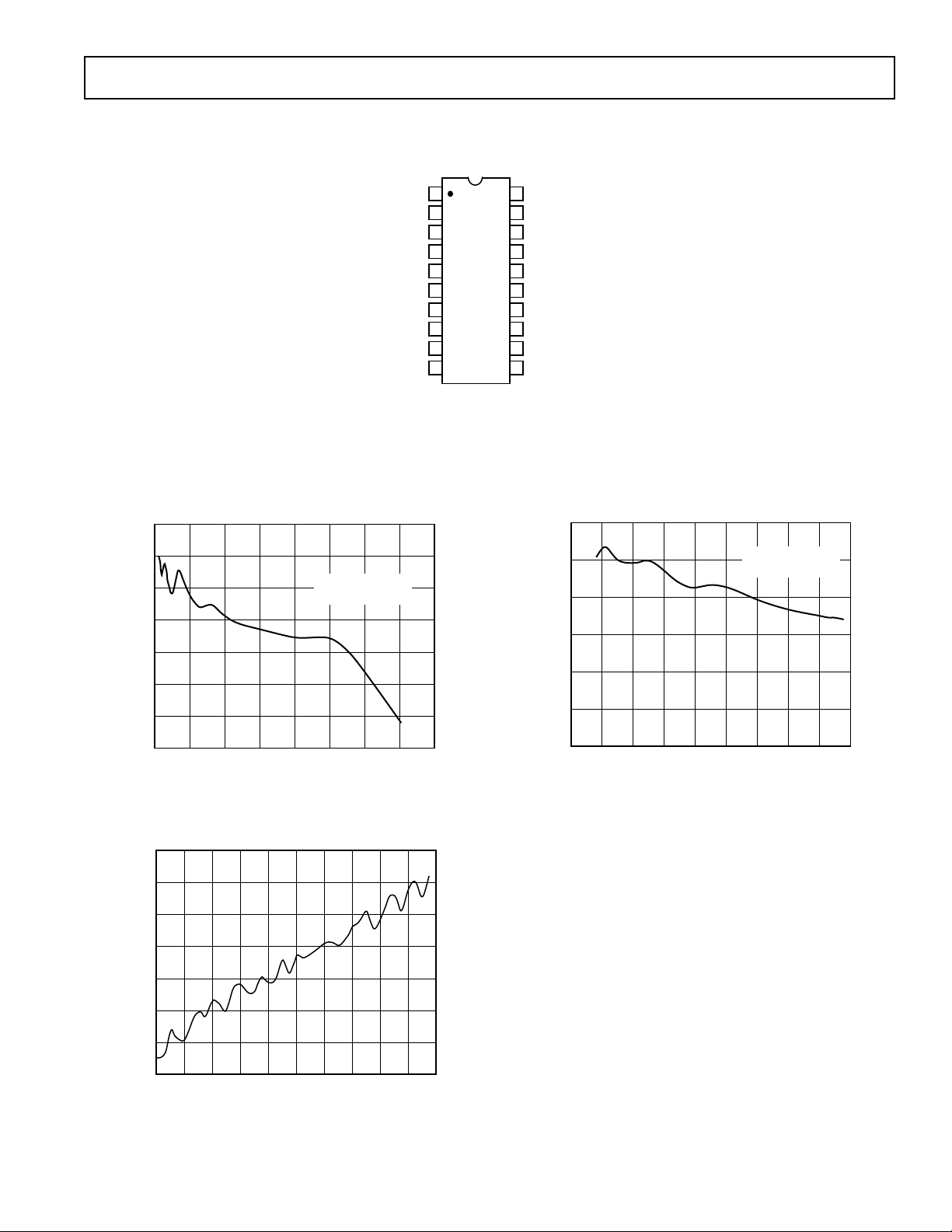
Figure 1. PSR as a Function of VDD 50 Hz Ripple
0.6
0.4
0.2
0
–0.2
Degrees
–0.4
–0.6
–0.8
45 5346 47 48 49 50 51 52
Figure 2. Phase Error as a Function of Line Frequency
50Hz RIPPLE – V rms
LINE FREQUENCY – Hz
Figure 3. PSR as a Function of VDD 50 Hz Ripple
54 55
–5–REV. 0
 Loading...