Analog Devices AD775 Datasheet

8-Bit 20 MSPS, 60 mW
1
2
7
8
3
4
5
6
9
10
151614
13
12
11
19
20
17
18
21
24
23
22
CLOCK LOGIC
FINE COMPARATORS
BANK B
FINE COMPARATORS
BANK A
COARSE
COMPARATORS
CORRECTION LOGIC
AV
DD
AV
SS
3-STATE OUTPUT LATCHES
D7 (MSB)
D0 (LSB)
RREF
15
SWITCH
MATRIX
V
RTS
V
RT
V
RB
V
RBS
OE
AV
SS
CLK DV
SS
AV
DD
V
IN
DV
DD
AD775
4
8
5
255
LSB MULTIPLEXOR
a
FEATURES
CMOS 8-Bit 20 MSPS Sampling A/D Converter
Low Power Dissipation: 60 mW
+5 V Single Supply Operation
Differential Nonlinearity: 0.3 LSB
Differential Gain: 1%
Differential Phase: 0.5 Degrees
Three-State Outputs
On-Chip Reference Bias Resistors
Adjustable Reference Input
Video Industry Standard Pinout
Small Packages:
24-Pin 300 Mil SOIC Surface Mount
24-Pin 400 Mil Plastic DIP
PRODUCT DESCRIPTION
The AD775 is a CMOS, low power, 8-bit, 20 MSPS sampling
analog-to-digital converter (ADC). The AD775 features a builtin sampling function and on-chip reference bias resistors to provide a complete 8-bit ADC solution. The AD775 utilizes a
pipelined/ping pong two-step flash architecture to provide high
sampling rates (up to 35 MHz) while maintaining very low
power consumption (60 mW).
Its combination of excellent DNL, fast sampling rate, low differential gain and phase errors, extremely low power dissipation,
and single +5 V supply operation make it ideally suited for a
variety of video and image acquisition applications, including
portable equipment. The AD775’s reference ladder may be connected in a variety of configurations to accommodate different
input ranges. The low input capacitance (11 pF typical) provides
an easy-to-drive input load compared to conventional flash
converters.
The AD775 is offered in both 300 mil SOIC and 400 mil DIP
plastic packages, and is designed to operate over an extended
commercial temperature range (–20°C to +75°C).
Sampling A/D Converter
AD775
FUNCTIONAL BLOCK DIAGRAM
PRODUCT HIGHLIGHTS
Low Power: The AD775 has a typical supply current of 12 mA,
for a power consumption of 60 mW. Reference ladder current
is also low: 6.6 mA typical, minimizing the reference power
consumption.
Complete Solution: The AD775’s switched capacitor design
features an inherent sample/hold function: no external SHA is
required. On-chip reference bias resistors are included to allow
a supply-based reference to be generated without any external
resistors.
Excellent Differential Nonlinearity: The AD775 features a
typical DNL of 0.3 LSBs, with a maximum limit of 0.5 LSBs.
No missing codes is guaranteed.
Single +5 V Supply Operation: The AD775 is designed to operate on a single +5 V supply, and the reference ladder may be
configured to accommodate analog inputs inclusive of ground.
Low Input Capacitance: The 11 pF input capacitance of the
AD775 can significantly decrease the cost and complexity of
input driving circuitry, compared with conventional 8-bit flash
ADCs.
REV. 0
Information furnished by Analog Devices is believed to be accurate and
reliable. However, no responsibility is assumed by Analog Devices for its
use, nor for any infringements of patents or other rights of third parties
which may result from its use. No license is granted by implication or
otherwise under any patent or patent rights of Analog Devices.
One Technology Way, P.O. Box 9106, Norwood, MA 02062-9106, U.S.A.
Tel: 617/329-4700 Fax: 617/326-8703

(TA = +258C with AVDD, DVDD = +5 V, AVSS, DVSS = 0 V, VRT = 2.6 V, VRB = +0.6 V,
AD775–SPECIFICA TIONS
CLOCK = 20 MHz unless otherwise noted)
AD775J
Parameter Min Typ Max Units
RESOLUTION 8 Bits
DC ACCURACY
Integral Nonlinearity (INL) +0.5 1.3 LSB
Differential Nonlinearity (DNL) ±0.3 ± 0.5 LSB
No Missing Codes GUARANTEED
Offset
To Top of Ladder V
To Bottom of Ladder V
VIDEO ACCURACY
RT
RB
1
–10 –35 –60 mV
0 +15 +45 mV
Differential Gain Error 1.0 %
Differential Phase Error 0.5 Degrees
ANALOG INPUT
Input Range (V
) 2.0 V p-p
RT–VRB
Input Capacitance 11 pF
AC SPECIFICATIONS
2
Signal-to-Noise and Distortion (S/(N + D))
f
= 1 MHz 47 dB
IN
f
= 5 MHz 41 dB
IN
Total Harmonic Distortion (THD)
f
= 1 MHz –51 dB
IN
fIN = 5 MHz –42 dB
REFERENCE INPUT
Reference Input Resistance (R
Case 1: V
RT
= V
, VRB = V
RTS
) 230 300 450 Ω
REF
RBS
Reference Bottom Voltage (VRB) 0.60 0.64 0.68 V
Reference Span (V
Reference Ladder Current (I
Case 2: V
RT
= V
RTS
) 1.96 2.09 2.21 V
RT–VRB
, VRB = AV
) 4.4 7.0 9.6 mA
REF
SS
Reference Span (VRT–VRB) 2.25 2.39 2.53 V
Reference Ladder Current (I
) 5811 mA
REF
POWER SUPPLIES
Operating Voltages
AV
DV
DD
DD
+4.75 +5.25 Volts
+4.75 +5.25 Volts
Operating Current
IAV
DD
IDV
DD
IAVDD + IDV
DD
9.5 mA
2.5 mA
12 17 mA
POWER CONSUMPTION 60 85 mW
TEMPERATURE RANGE
Operating –20 +75 °C
NOTES
1
NSTC 40 IRE modulation ramp, CLOCK = 14.3 MSPS.
2
fIN amplitude = 0.3 dB full scale.
Specifications subject to change without notice. See Definition of Specifications for additional information.
–2–
REV. 0

(TA = +258C with AVDD, DVDD = +5 V, AVSS, DVSS = 0 V, VRT = 2.6 V, VRB = +0.6 V,
DIGITAL SPECIFICATIONS
CLOCK = 20 MHz unless otherwise noted)
Parameter Symbol DV
LOGIC INPUT
High Level Input Voltage V
Low Level Input Voltage V
IH
IL
5.0 4.0 V
5.0 1.0 V
High Level Input Current
(V
= DVDD)I
IH
IH
5.25 5 µA
Low Level Input Current
(V
= 0 V) I
IL
Logic Input Capacitance C
IL
IN
5.25 –5 µA
LOGIC OUTPUTS
High Level Output Current
OE = DVSS, VOH = DVDD–0.5 V I
OE = DVDD, VOH = DV
DD
OH
I
OZ
4.75 –1.1 mA
5.25 16 µA
Low Level Output Current
OE = DVSS, VOL = 0.4 V I
OE = DVDD, VOL = 0 V I
OL
OZ
4.75 3.7 mA
5.25 16 µA
TIMING SPECIFICATIONS
Symbol Min Typ Max Units
DD
AD775
AD775J
Min Typ Max Units
5pF
Maximum Conversion Rate 20 35 MHz
Clock Period t
Clock High t
Clock Low t
Output Delay t
C
CH
CL
OD
50 ns
25 ns
25 ns
18 30 ns
Pipeline Delay (Latency) 2.5 Clock Cycles
Sampling Delay t
DS
4ns
Aperture Jitter 30 ps
Specifications subject to change without notice.
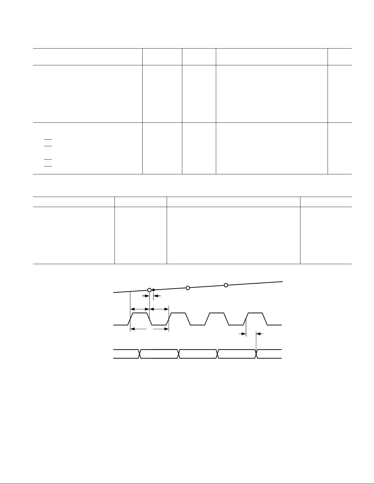
SAMPLE N+2
t
OD
VIN
CLK
OUT
t
DS
SAMPLE N+1
SAMPLE N
t
CH
t
CL
t
C
DATA N-3 DATA N-2 DATA N-1 DATA N
Figure 1. AD775 Timing Diagram
REV. 0
–3–

AD775
WARNING!
ESD SENSITIVE DEVICE
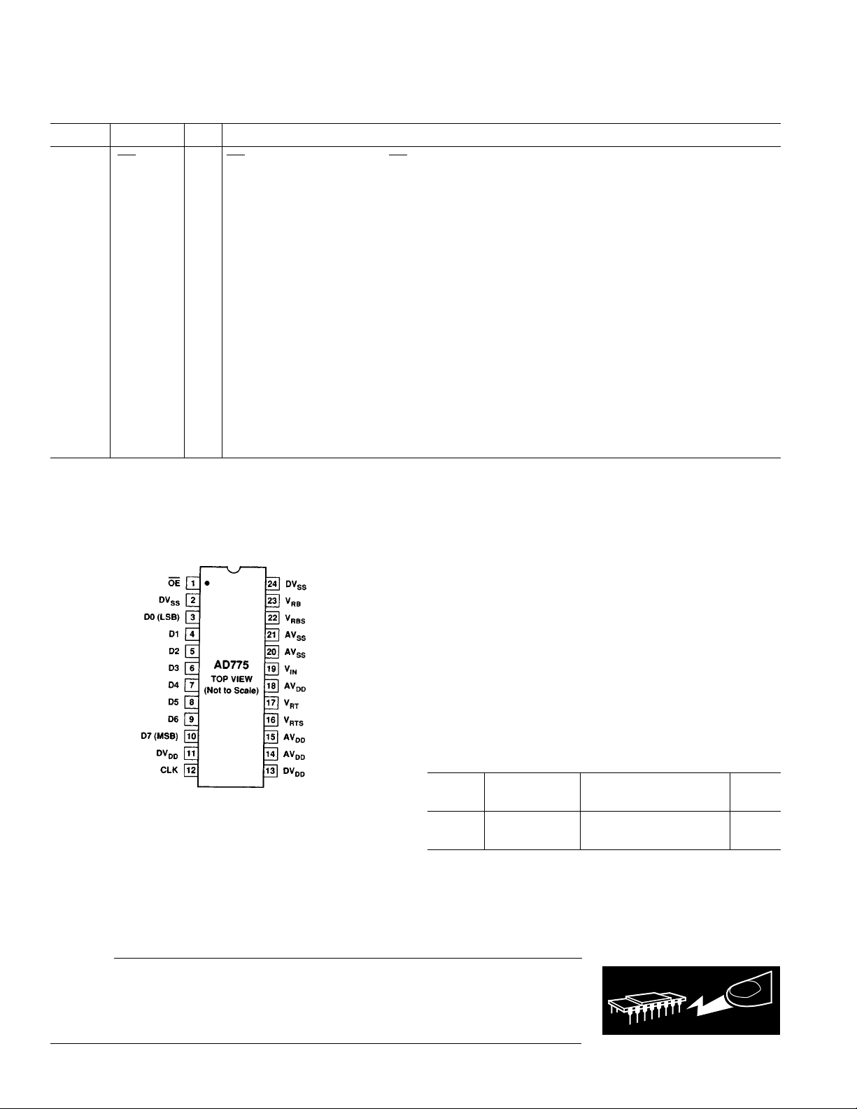
Pin No. Symbol Type Name and Function
PIN DESCRIPTION
1
OE DI OE = Low OE = High
Normal Operating Mode. High Impedance Outputs.
2, 24 DV
SS
P Digital Ground. Note: DVSS and AVSS pins should share a common ground plane on the circuit board.
3 D0 (LSB) DO Least Significant Bit, Data Bit 0.
4–9 D1–D6 DO Data Bits 1 Through 6.
10 D7 (MSB) DO Most Significant Bit, Data Bit 7.
11, 13 DV
DD
P +5 V Digital Supply. Note: DVDD and AVDD pins should share a common supply on the circuit board.
12 CLK DI Clock Input.
16 V
17 V
23 V
22 V
14, 15, 18 AV
RTS
RT
RB
RBS
DD
AI Reference Top Bias. Short to VRT for Self-Bias.
AI Reference Ladder Top.
AI Reference Ladder Bottom.
AI Reference Bottom Bias. Short to VRB for Self-Bias.
P +5 V Analog Supply. Note: DVDD and AVDD pins should share a common supply within 0.5 inches
of the AD775.
19 V
20, 21 AV
IN
SS
AI Analog Input. Input Span = VRT–VRB.
P Analog Ground. Note: DVSS and AVSS pins should share a common ground within 0.5 inches of the
AD775.
NOTE
Type: AI = Analog Input; DI = Digital Input; DO = Digital Output; P = Power.
PIN CONFIGURATION
(DIP and SOIC)
MAXIMUM RATINGS*
Supply Voltage (AVDD, DVDD) . . . . . . . . . . . . . . . . . . . . 7 V
Supply Difference (AV
Ground Difference (AV
Reference Voltage (V
Analog Input Voltage (VIN) . . . . . . . . . . . . . . . . . . VDD to V
Digital Input Voltage (CLK) . . . . . . . . . . . . . . . . . VDD to V
Digital Output Voltage (VOH, VOL) . . . . . . . . . . . . VDD to V
–DVDD) . . . . . . . . . . . . . . . . . . 0 V
DD
–DVSS) . . . . . . . . . . . . . . . . . . . 0 V
SS
, VRB) . . . . . . . . . . . . . . . . VDD to V
RT
SS
SS
SS
SS
Storage Temperature . . . . . . . . . . . . . . . . . . –55°C to +150°C
*Stresses above those listed under “Absolute Maximum Ratings” may cause
permanent damage to the device. This is a stress rating only and functional
operation of the device at these or any other conditions above those indicated in the
operational sections of this specification is not implied. Exposure to absolute
maximum rating conditions for extended periods may affect device reliability.
Temperature Package Package
Model Range Description Option
AD775JN –20°C to +75°C 24-Pin 400 Mil Plastic DIP N-24B
AD775JR –20°C to +75°C 24-Pin 300 Mil SOIC R-24A
CAUTION
ESD (electrostatic discharge) sensitive device. Electrostatic charges as high as 4000 V readily
accumulate on the human body and test equipment and can discharge without detection.
Although the AD775 features proprietary ESD protection circuitry, permanent damage may
occur on devices subjected to high energy electrostatic discharges. Therefore, proper ESD
precautions are recommended to avoid performance degradation or loss of functionality.
–4–
ORDERING GUIDE
REV. 0
 Loading...