Analog Devices AD7747 prb Datasheet

24-bit Capacitance to Digital Converter
Preliminary Technical Data
FEATURES
Capacitance to Digital Converter (CDC)
Standard One Chip Solution
Interfaces to Single or Differential Grounded Sensors
Resolution: 40 aF (i.e. 18-bit) at 16.6 Hz
Accuracy: 4 fF
Linearity: 0.01%
Input Range: ±8 pF
Offset / Common Capacitance Removal: up to 17 pF
Update rate: 5 Hz to 90 Hz
Simultaneous 50 Hz and 60 Hz rejection at 16.6 Hz
Tolerant of ground capacitance and ground leakage
current
Temperature sensor on chip
Resolution: 0.1°C, accuracy: ±2°C
Voltage input channel
Internal clock oscillator
2
2-Wire Serial Interface (I
C®-Compatible)
Power
2.7 V to 5.25 V Single-Supply Operation
1 mA Current Consumption
Operating temperature: -40°C to +125°C
Package: 16-lead TSSOP
APPLICATIONS
Automotive, Industrial and Medical Systems for:
Pressure Measurement
Position Sensors
Level Sensors
Flowmeters
Humidity Sensors
Impurity Detection
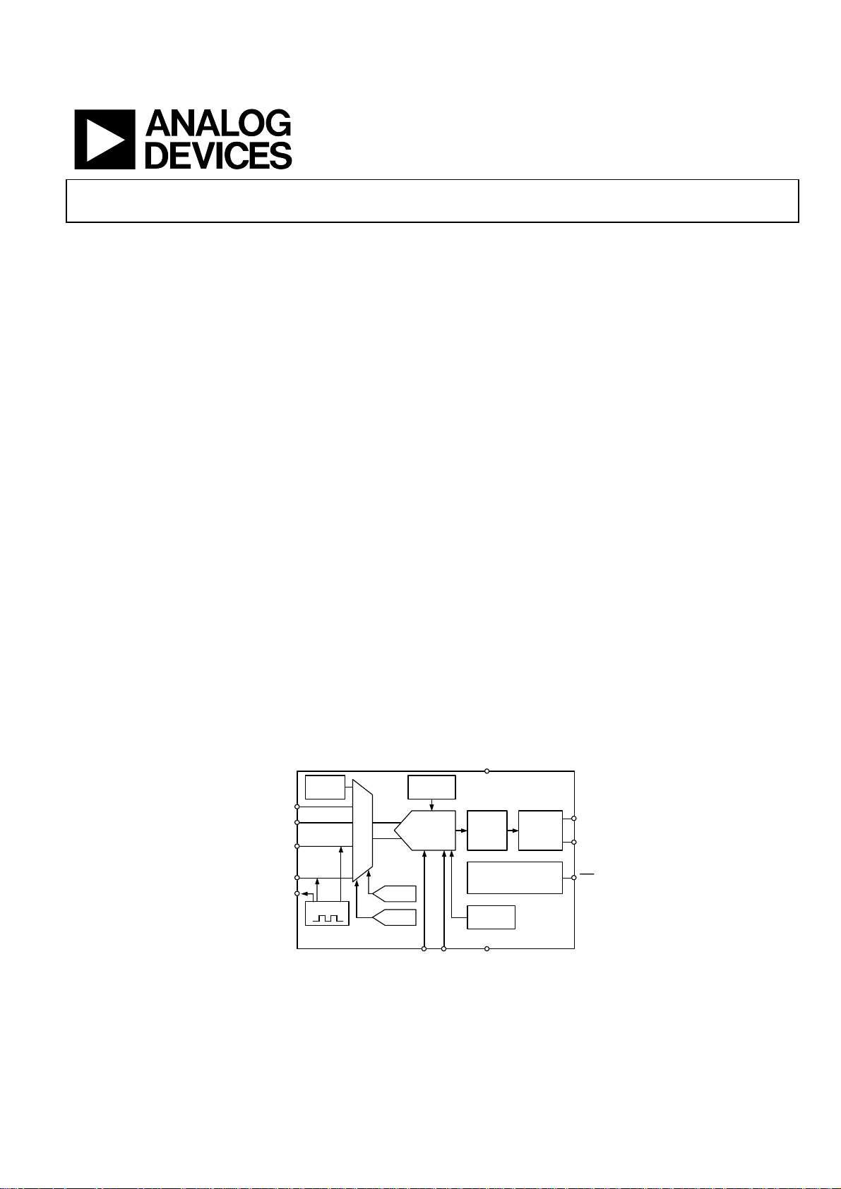
FUNCTIONAL BLOCK DIAGRAMS
TEMP
SENSOR
VIN(+)
VIN(
-
)
C
(+)
IN1
MUX
CLOCK
GENERATOR
24-BITΣ-
MODULATOR
with Temperature Sensor
AD7747
GENERAL DESCRIPTION
The AD7747 is a high-resolution Σ−∆ capacitance to digital
converter (CDC). The capacitance to be measured is connected
directly to the device inputs. The architecture features inherent
high resolution (24-bit no missing codes, 18-bit effective
resolution at 16.6 Hz data rate), high linearity (±0.01%) and
high accuracy (±4 fF factory calibrated). The AD7747
capacitance input range is ±8 pF (changing), while it can accept
up to 17 pF absolute capacitance (not changing), which is
compensated by an on-chip digital to capacitance converter
(CAPDAC).
The AD7747 is designed for single ended or differential
capacitive sensors with one plate connected to ground.
For floating capacitive sensors, the AD7745 or AD7746 are
recommended.
The part has an on-chip temperature sensor with resolution of
0.1°C and accuracy of ±2°C. The on-chip voltage reference and
the on-chip clock generator eliminate the need for any external
components in most capacitive sensor applications. The part
has a standard voltage input, which together with the
differential reference input allows easy interface to an external
temperature sensor, such as an RTD, thermistor or diode.
The AD7747 has a 2-wire, I
part operates from a single 3 V or 5 V power supply. It is
specified over the automotive temperature range of -40°C to
+125°C and is housed in a 16-lead TSSOP package.
V
DD
AD7747
∆
DIGITAL
FILTER
I2C
SERIAL
INTERFACE
2
C compatible serial interface. The
SDA
SCL
C
(
-
)
IN1
SHLD
EXCITATION
Rev. PrB, 3. March 2005
Information furnished by Analog Devices is believed to be accurate and reliable.
However, no responsibility is assumed by Analog Devices for its use, nor for any
infringements of patents or other rights of third parties that may result from its use.
Specifications subject to change without notice. No license is granted by implication
or otherwise under any patent or patent rights of Analog Devices. Trademarks and
registered trademar ks are the property of their respective companies.
CAP DAC 1
CAP DAC 2
REFIN(+) REFIN(-)
Figure 1.
One Technology Way, P.O. Box 9106, Norwood, MA 02062-9106, U.S.A.
Tel: 781.329.4700
Fax: 781.326.8703 © 2005 Analog Devices, Inc. All rights reserved.
CONTROL LOGIC
CALIBRATION
VOLTAGE
REFERENCE
GND
RDY
www.analog.com

AD7747
TABLE OF CONTENTS
AD7747—PRELIMINARY SPECIFICATIONS ........................... 3
Timing Specifications....................................................................... 5
Absolute Maximum Ratings............................................................ 5
Pin Configuration and Function Descriptions............................. 6
SERIAL INTERFACE....................................................................... 7
Write Operation............................................................................ 7
Read Operation............................................................................. 7
General Call................................................................................... 8
AD7747 Reset................................................................................ 8
REGISTER DESCRIPTIONS.......................................................... 9
Status Register............................................................................. 10
Cap Data Register....................................................................... 10
VT Data Register ........................................................................10
Cap Setup Register ..................................................................... 11
VT Setup Register....................................................................... 11
Exc Setup Register ...................................................................... 12
Configuration Register .............................................................. 13
Cap DAC A Register................................................................... 14
Cap DAC B Register................................................................... 14
Cap Offset Register..................................................................... 14
Cap Gain Register....................................................................... 14
Volt Gain Register....................................................................... 14
Typical Application Diagram ........................................................ 15
Outline Dimensions....................................................................... 16
ESD Caution................................................................................ 16
Preliminary Technical Data
Rev. PrB | Page 2 of 16

Preliminary Technical Data
AD7747
AD7747—PRELIMINARY SPECIFICATIONS
Table 1. (VDD = 2.7 V to 3.3 V, or 4.75V to 5.25V, GND = 0 V, –40°C to +125°C, unless otherwise noted.)
Parameter Min Typ Max Unit Test Conditions/Comments
CAPACITIVE INPUT (INPUTS)
Conversion Input Range ±8.192 pF Factory calibrated
Integral Nonlinearity (INL) 1 ±0.01 % of FSR
No-missing Codes 1 24 bit 62ms conversion time
Resolution p-p 16 bit 62ms conversion time
Resolution effective 18 bit 62ms conversion time
Output Noise rms 10
Absolute Error 2 ±4 fF 25°C, after offset calibration
Offset Error TBD aF After system offset calibration
Offset Drift vs. Temperature TBD fF/°C
Gain Error TBD % of FS
Gain Drift vs. Temperature 1 -27 ppm of FS/°C
Power Supply Rejection TBD fF/V
Conversion Time 22.0 219.2 ms Configurable via digital interface
CAPDAC
Full Range 17 21 pF
Resolution 3 330 fF 6-bit CAPDAC
Drift vs. Temperature 1 +27 ppm of FS/°C
EXCITATION
Frequency 16 kHz
Voltage across Capacitance ± VDD /8 V Configurable via digital interface
± VDD /4 V
± VDD /2 V
ACTIVE SHIELDING SHLD pin
Allowed Capacitance to GND 1 50 pF
TEMPERATURE SENSOR 4 VTCHOP
Resolution 0.1 °C
Error 1 ±0.5 ±2 °C Internal temperature sensor
±2 ±4 °C External sensing diode
VOLTAGE INPUT 4
Differential VIN Voltage Range ±V
Absolute VIN Voltage GND –0.03 VDD +0.03 V
Integral Nonlinearity (INL) 1 ±5 ±15 ppm of FSR
No-missing Codes 1 24 bit 62ms conversion time
Resolution p-p 16 bits 62ms conversion time
Output Noise 3 µV rms 62ms conversion time
Offset Error ±3 µV
Offset Drift vs. Temperature 15 nV/°C
Full-Scale Error 5 ±10 µV
Full-Scale Drift vs. Temperature TBD ppm of FSR/°C External reference
Average VIN Input Current 400 nA/V
Analog VIN Input Current Drift ±50 pA/V/°C
Power Supply Rejection 90 dB External reference
Power Supply Rejection 80 dB Internal reference
Common-Mode Rejection 90 dB
Conversion Time 20.1 122.1 ms Configurable via Digital Interface
× 3/8
± V
DD
V
REF
V
aF/√Hz
62ms conversion time
62ms conversion time
4
= 1
Rev. PrB | Page 3 of 16

AD7747
Preliminary Technical Data
Parameter Min Typ Max Unit Test Conditions/Comments
INTERNAL VOLTAGE REFERENCE
Voltage 1.168 1.17 1.172 V At VDD = 4V, TA = 25°C
Drift vs. Temperature 10 ppm/°C
EXTERNAL VOLTAGE REFERENCE INPUT
Differential REFIN Voltage 1 0.1 2.5 VDD V
Absolute REFIN Voltage GND –0.03 VDD +0.03 V
Average REFIN Input Current ±400 nA/V
Average REFIN Input Current Drift ±50 pA/V/°C
SERIAL INTERFACE
LOGIC INPUTS (SCL, SDA)
VIH Input High Voltage 2.1 V
VIL Input Low Voltage 0.8 V
Hysteresis 150 mV
OPEN-DRAIN OUTPUT (SDA)
VOL Output Low Voltage 0.4 V
IOH Output High Leakage Current 0.1 1 µA V
LOGIC OUTPUT (
RDY
)
VOL Output Low Voltage 0.4 V I
VOH Output High Voltage 4.0 V I
VOL Output Low Voltage 0.4 V I
VOH Output High Voltage DVDD – 0.6 V I
I
= −6.0 mA
SINK
= VDD
OUT
= 1.6 mA, VDD = 5 V
SINK
= 200 µA, VDD = 5 V
SOURCE
= 100 µA, VDD = 3 V
SINK
= 100 µA, VDD = 3 V
SOURCE
POWER REQUIREMENTS
VDD to GND Voltage 4.75 5.25 V VDD = 5 V nominal
2.7 3.3 V VDD = 3 V nominal
IDD Current 1 mA Digital inputs equal to VDD or GND
IDD Current Power Down Mode 1 µA Digital inputs equal to VDD or GND
1
Specification is not production tested, but is supported by characterization data at initial product release.
2
Factory calibrated The absolute error includes factory gain calibration error, integral nonlinearity error, and offset error after system offset calibration, all at 25°C.
At different temperatures, compensation for gain drift over temperature is required.
3
The CAPDAC resolution is 6-bit in the actual CAPDAC full range. Using the on-chip offset calibration or adjusting the capacitive offset calibration register can further
reduce the CIN offset or the non-changing CIN component.
4
The VTCHOP bit in the VT SETUP register must be set to 1 for the specified temperature sensor and voltage input performance.
5
Full-scale error applies to both positive and negative full-scale.
Rev. PrB | Page 4 of 16

Preliminary Technical Data
A
AD7747
TIMING SPECIFICATIONS
Table 2. (VDD = 2.7 V to 3.3 V, or 4.75V to 5.25V, GND = 0 V; Input Logic 0 = 0 V; Input Logic 1 = VDD; –40°C to +125°C, unless otherwise noted.)
Parameter Min Typ Max Unit Test Conditions/Comments
SERIAL INTERFACE
SCL Frequency 0 400 kHz
SCL High Pulse Width, t
SCL Low Pulse Width, t
SCL, SDA Rise Time, tR 0.3 µs
SCL, SDA Fall Time, t
Hold Time (Start Condition), t
Setup Time (Start Condition), t
Data Setup Time, t
Setup Time (Stop Condition), t
Data Hold Time, t
Bus Free Time (Between Stop and Start Condition, t
1
Sample tested during initial release to ensure compliance.
2
All input signals are specified with input rise/fall times = 3 ns, measured between the 10% and 90% points. Timing reference points at 50% for inputs and outputs.
Output load = 10 pF.
1, 2
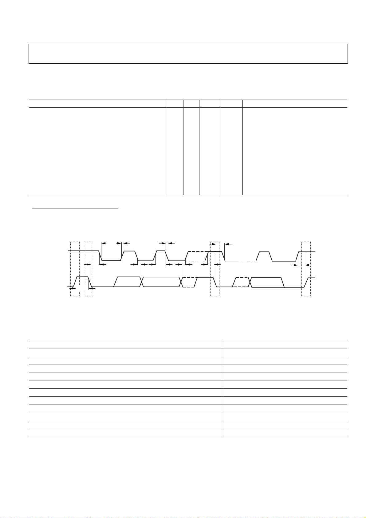
See Figure 2
0.6 µs
HIGH
1.3 µs
LOW
F
0.6 µs After this period, the first clock is generated
HD;STA
0.6 µs Relevant for repeated start condition
SU;STA
0.1 µs
SU;DAT
0.6 µs
SU;STO
(Master) 0 µs
HD;DAT
t
R
t
LOW
0.3 µs
1.3 µs
BUF
t
F
t
HD:STA
SCL
SD
t
t
BUF
PS
HD:STA
t
HD:DAT
t
HIGH
t
SU:DAT
Figure 2.Serial Inter face Timing Diagram
t
SU:STA
S
t
SU:STO
P
04918-0-002
ABSOLUTE MAXIMUM RATINGS
Table 3. (TA = 25°C, unless otherwise noted.)
Parameter Rating
Positive Supply Voltage VDD to GND
Voltage on any input or output pin to GND –0.3 V to VDD + 0.3 V
ESD Rating (ESD Association Human Body Model, S5.1) TBD V
Operating Temperature Range –40°C to +125°C
Storage Temperature Range –65°C to +150°C
Junction Temperature 150°C
TSSOP Package θJA Thermal Impedance to Air
TSSOP Package θJC Thermal Impedance to Case
Lead Temperature, Soldering
Vapor Phase (60 sec) 215°C
Infrared (15 sec) 220°C
Stresses above those listed under Absolute Maximum Ratings may cause permanent damage to the device. This is a stress rating only;
functional operation of the device at these or any other conditions above those indicated in the operational section of this specification is
not implied. Exposure to absolute maximum rating conditions for extended periods may affect device reliability.
−0.3 V to +6.5 V
128 °C/W
14 °C/W
Rev. PrB | Page 5 of 16
 Loading...