CMOS 12-Bit
a
FEATURES
12-Bit Resolution
Low Gain TC: 2 ppm/ⴗC typ
Fast TTL Compatible Data Latches
Single +5 V to +15 V Supply
Small 20-Lead 0.3" DIP and 20-Terminal Surface Mount
Packages
Latch Free (Schottky Protection Diode Not Required)
Low Cost
Ideal for Battery Operated Equipment
GENERAL DESCRIPTION
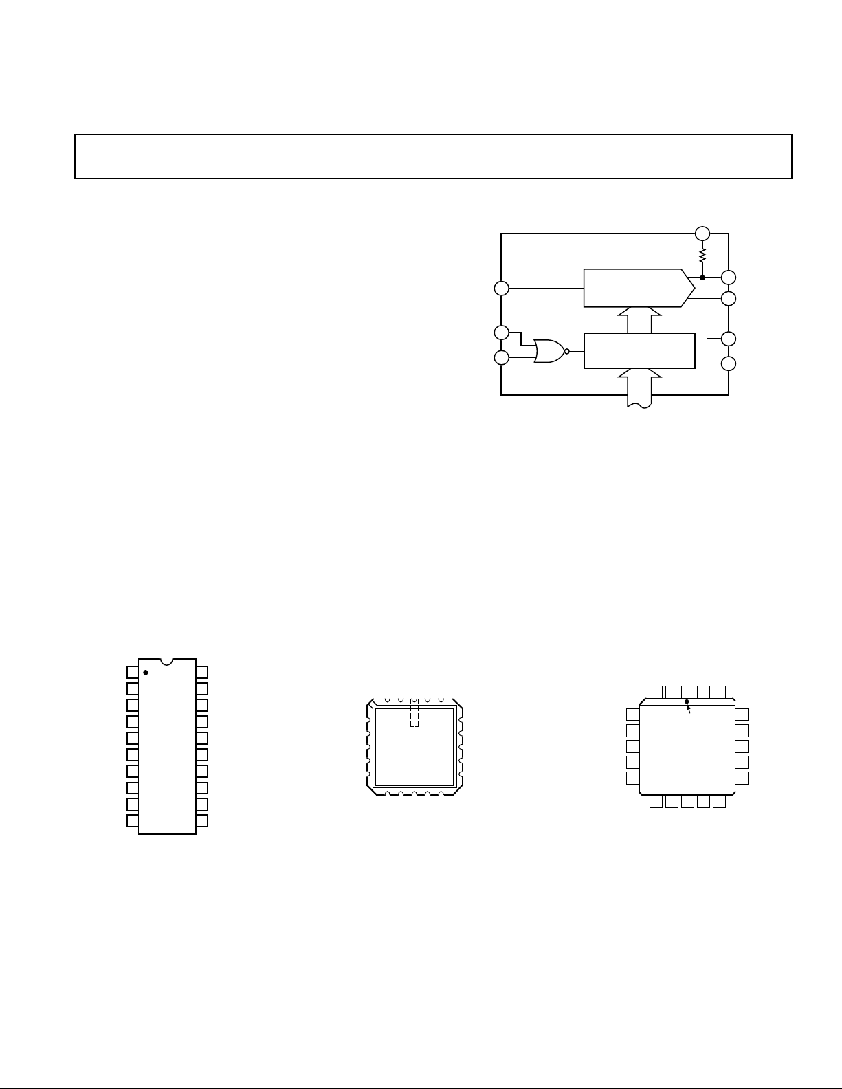
The AD7545 is a monolithic 12-bit CMOS multiplying DAC
with onboard data latches. It is loaded by a single 12-bit wide
word and directly interfaces to most 12- and 16-bit bus systems.
Data is loaded into the input latches under the control of the CS
and WR inputs; tying these control inputs low makes the input
latches transparent, allowing direct unbuffered operation of the
DAC.
Buffered Multiplying DAC
AD7545
FUNCTIONAL BLOCK DIAGRAM
R
FB
20
AD7545
V
19
REF
17
WR
16
CS
12-BIT
MULTIPLYING DAC
12
INPUT DATA LATCHES
12
DB11–DB0
(PINS 4–15)
The AD7545 is particularly suitable for single supply operation
and applications with wide temperature variations.
The AD7545 can be used with any supply voltage from +5 V to
+15 V. With CMOS logic levels at the inputs the device dissipates less than 0.5 mW for V
= +5 V.
DD
R
1
OUT 1
2
AGND
18
V
DD
3
DGND
PIN CONFIGURATIONS
DIP LCCC PLCC
OUT 1
AGND
DGND
DB11 (MSB)
DB9
DB8
DB7
DB6
DB5
1
2
3
4
5
AD7545
TOP VIEW
6
(Not to Scale)
7
8
9
10
20
R
19
V
18
V
17
WR
16
CSDB10
DB0 (MSB)
15
DB1
14
DB2
13
12
DB3
11
DB4
FB
REF
DD
DB11 (MSB)
DB10
DB9
DB8
DB7
3
4
5
6
7
8
9 10111213
AGND
DGND
2
AD7545
TOP VIEW
(Not to Scale)
DB6
DB5
REV. A
Information furnished by Analog Devices is believed to be accurate and
reliable. However, no responsibility is assumed by Analog Devices for its
use, nor for any infringements of patents or other rights of third parties
which may result from its use. No license is granted by implication or
otherwise under any patent or patent rights of Analog Devices.
FB
R
OUT 1
20 191
DB4
FB
DB3
REF
V
DB2
18
V
17
WR
16
CS
15
DB0 (LSB)
DB1
14
AGND
DGND
2
3
DB10
DB9
DB8
DB7
4
5
6
7
8
AD7545
TOP VIEW
(Not to Scale)
9
10 11 12 13
DB6
DB5
DD
DB11 (MSB)
OUT 1
20 19
1
PIN 1
IDENTIFIER
DB4
R
DB3
REF
V
DB2
One Technology Way, P.O. Box 9106, Norwood, MA 02062-9106, U.S.A.
Tel: 617/329-4700 World Wide Web Site: http://www.analog.com
Fax: 617/326-8703 © Analog Devices, Inc., 1997
18
17
16
15
14
V
DD
WR
CS
DB0 (LSB)
DB1

AD7545–SPECIFICATIONS
= +10 V, V
REF
= O V, AGND = DGND unless otherwise noted)
OUT1
(V
VDD = +5 V VDD = +15 V
Parameter Version TA = + 25ⴗCT
Limits Limits
MIN, TMAX
1
TA = + 25ⴗCT
MIN, TMAX
1
Units Test Conditions/Comments
STATIC PERFORMANCE
Resolution All 12 12 12 12 Bits
J, A, S ±2 ±2 ±2 ±2 LSB max
K, B, T ±1 ±1 ±1 ±1 LSB max
L, C, U ±1/2 ±1/2 ±1/2 ±1/2 LSB max
GL, GC, GU ±1/2 ±1/2 ±1/2 ±1/2 LSB max
Differential Nonlinearity J, A, S ±4 ±4 ±4 ±4 LSB max 10-Bit Monotonic T
K, B, T ±1 ±1 ±1 ±1 LSB max 12-Bit Monotonic T
L, C, U ±1 ±1 ±1 ±1 LSB max 12-Bit Monotonic T
GL, GC, GU ±1 ±1 ±1 ±1 LSB max 12-Bit Monotonic T
Gain Error (Using Internal RFB)2J, A, S ±20 ±20 ± 25 ±25 LSB max DAC Register Loaded with
MIN
MIN
MIN
MIN
to T
to T
to T
to T
MAX
MAX
MAX
MAX
K, B, T ±10 ±10 ± 15 ±15 LSB max 1111 1111 1111
L, C, U ±5 ±6 ±10 ±10 LSB max Gain Error Is Adjustable Using
Gain Temperature Coefficient
∆Gain/∆Temperature All ±5 ±5 ±10 ±10 ppm/°C max Typical Value is 2 ppm/°C for VDD = +5 V
DC Supply Rejection
∆Gain/∆V
Output Leakage Current at OUT1 J, K, L, GL 10 50 10 50 nA max DB0–DB11 = 0 V; WR, CS = 0 V
DD
3
3
GL, GC, GU ±1 ±2 ±6 ±7 LSB max the Circuits of Figures 4, 5, and 6
All 0.015 0.03 0.01 0.02 % per % max ∆VDD = ±5%
A, B, C, GC 10 50 10 50 nA max
S, T, U, GU 10 200 10 200 nA max
DYNAMIC PERFORMANCE
Current Settling Time
3
All 2 2 2 2 µs max To 1/2 LSB. OUT1 Load = 100 Ω. DAC
Output Measured from Falling Edge of
Propagation Delay
3
(from Digital
WR, CS = 0.
Input Change to 90%
of Final Analog Output) All 300 – 250 – ns max OUT1 Load = 100 Ω, C
Digital-to-Analog Glitch Inpulse All 400 – 250 – nV sec typ V
AC Feedthrough
5
At OUT1 All 5 5 5 5 mV p-p typ V
= AGND
REF
= ±10 V, 10 kHz Sinewave
REF
EXT
= 13 pF
REFERENCE INPUT
Input Resistance All 7 7 7 7 kΩ min Input Resistance TC = –300 ppm/°C typ
(Pin 19 to GND) 25 25 25 25 kΩ max Typical Input Resistance = 11 kΩ
ANALOG OUTPUT
Output Capacitance
C
OUT1
C
OUT1
3
All 70 70 70 70 pF max DB0–DB11 = 0 V, WR, CS = 0 V
200 200 200 200 pF max DB0–DB11 = VDD, WR, CS = 0 V
DIGITAL INPUTS
Input High Voltage
V
IH
Input Low Voltage
V
IL
Input Current
I
IN
Input Capacitance
6
3
All 2.4 2.4 13.5 13.5 V min
All 0.8 0.8 1.5 1.5 V max
All ±1 ±10 ± 1 ± 10 µA max VIN = 0 or V
DD
DB0–DB11 All 5 5 5 5 pF max VIN = 0
WR, CS All 20 20 20 20 pF max VIN = 0
SWITCHING CHARACTERISTICS
7
Chip Select to Write Setup Time All 280 380 180 200 ns min See Timing Diagram
t
CS
Chip Select to Write Hold Time
t
CH
Write Pulse Width
t
WR
All 0 0 0 0 ns min
All 250 400 160 240 ns min t
200 270 120 150 ns typ
175 280 100 170 ns typ
≥ tWR, tCH ≥ 0
CS
Data Setup Time All 140 210 90 120 ns min
t
DS
Data Hold Time
t
DH
All 10 10 10 10 ns min
100 150 60 80 ns typ
POWER SUPPLY
I
DD
NOTES
1
Temperature range as follows: J, K, L, GL versions, 0°C to +70°C; A, B, C, GC versions, –25°C to +85°C; S, T, U GU versions, –55°C to +125°C.
2
This includes the effect of 5 ppm max gain TC.
3
Guaranteed but not tested.
4
DB0–DB11 = 0 V to VDD or VDD to 0 V.
5
Feedthrough can be further reduced by connecting the metal lid on the ceramic package (Suffix D) to DGND.
6
Logic inputs are MOS gates. Typical input current (+25°C) is less than 1 nA.
7
Sample tested at +25°C to ensure compliance.
All 2 2 2 2 mA max All Digital Inputs VIL or V
100 500 100 500 µA max All Digital Inputs 0 V to V
10 10 10 10 µA typ All Digital Inputs 0 V to V
IH
DD
DD
Specifications subject to change without notice.
–2–
REV. A
4

AD7545
WARNING!
ESD SENSITIVE DEVICE
CHIP
SELECT
WRITE
DATA IN
(DB0–DB11)
t
CS
V
IH
V
IL
t
WR
t
DS
DATA VALID
t
CH
t
DH
V
DD
0
V
DD
0
V
DD
0
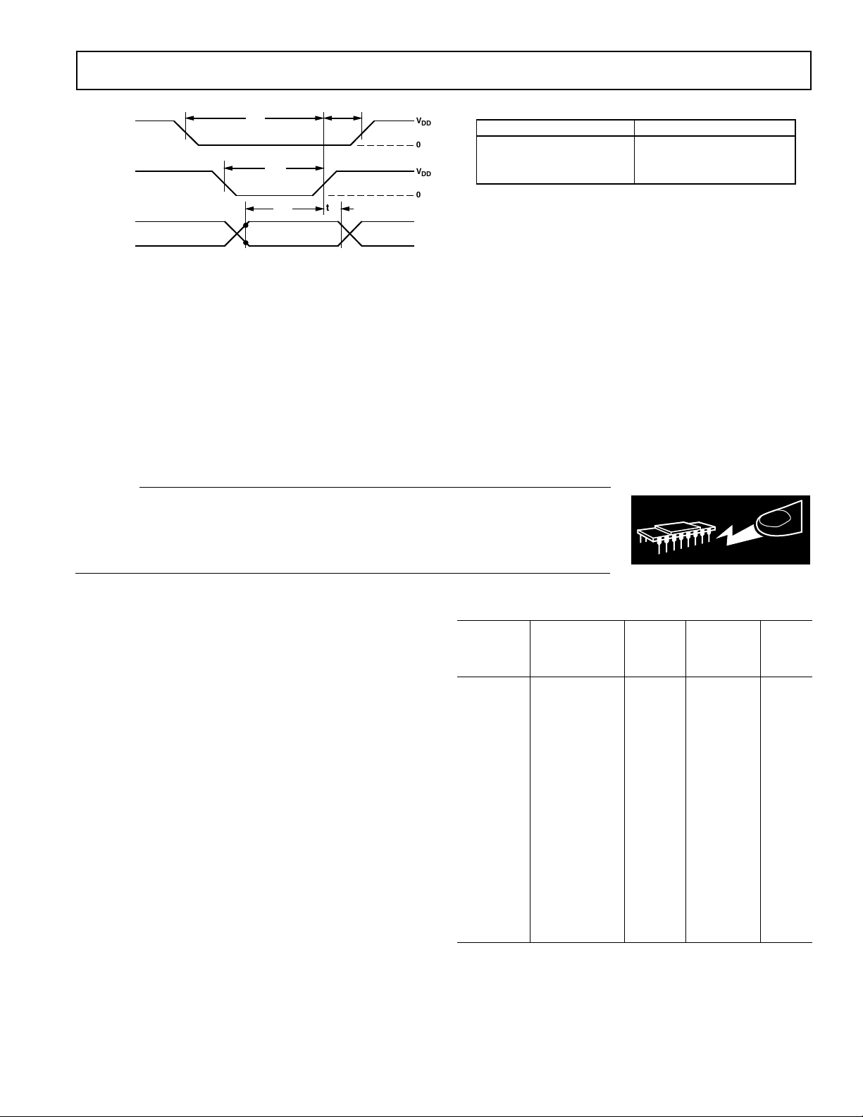
WRITE MODE:
CS AND WR LOW, DAC RESPONDS
TO DATA BUS (DB0–DB11) INPUTS.
NOTES:
V
= +5V; tr = tf = 20ns
DD
VDD = +15V; tr = tf = 40ns
ALL INPUT SIGNAL RISE AND FALL TIMES MEASURED FROM 10% TO
90% OF V
TIMING MEASUREMENT REFERENCE LEVEL IS VIH + VIL/2.
.
DD
MODE SELECTION
Write Cycle Timing Diagram
ABSOLUTE MAXIMUM RATINGS*
(TA = + 25°C unless otherwise noted)
V
to DGND . . . . . . . . . . . . . . . . . . . . . . . . . . . –0.3, +17 V
DD
Digital Input Voltage to DGND . . . . . . . –0.3 V, V
V
, V
to DGND . . . . . . . . . . . . . . . . . . . . . . . . . ±25 V
REF
to DGND . . . . . . . . . . . . . . . . . . . . –0.3 V, VDD +0.3 V
V
RFB
PIN1
AGND to DGND . . . . . . . . . . . . . . . . . –0.3 V, V
+0.3 V
DD
+ 0.3 V
DD
Power Dissipation (Any Package) to +75°C . . . . . . . 450 mW
Derates above +75°C . . . . . . . . . . . . . . . . . . . . . . 6 mW/°C
Commercial (J, K, L, GL) Grades . . . . . . . . 0°C to +70°C
Industrial (A, B, C, GC) Grades . . . . . . . . –25°C to +85°C
Extended (S, T, U, GU) Grades . . . . . . . –55°C to +125°C
Storage Temperature . . . . . . . . . . . . . . . . . . –65°C to +150°C
Lead Temperature (Soldering, 10 secs) . . . . . . . . . . . +300°C
*Stresses above those listed under Absolute Maximum Ratings may cause perma-
nent damage to the device. This is a stress rating only; functional operation of the
device at these or any other conditions above those indicated in the operational
sections of this specification is not implied. Exposure to absolute maximum rating
conditions for extended periods may affect device reliability.
Operating Temperature
CAUTION
ESD (electrostatic discharge) sensitive device. Electrostatic charges as high as 4000 V readily
accumulate on the human body and test equipment and can discharge without detection.
Although the AD7545 features proprietary ESD protection circuitry, permanent damage may
occur on devices subjected to high energy electrostatic discharges. Therefore, proper ESD
precautions are recommended to avoid performance degradation or loss of functionality.
HOLD MODE:
EITHER CS OR WR HIGH, DATA BUS
(DB0–DB11) IS LOCKED OUT; DAC
HOLDS LAST DATA PRESENT WHEN
WR OR CS ASSUMED HIGH STATE.
TERMINOLOGY
RELATIVE ACCURACY
The amount by which the D/A converter transfer function
differs from the ideal transfer function after the zero and fullscale points have been adjusted. This is an endpoint linearity
measurement.
DIFFERENTIAL NONLINEARITY
The difference between the measured change and the ideal
change between any two adjacent codes. If a device has a differential nonlinearity of less than 1 LSB it will be monotonic, i.e.,
the output will always increase for an increase in digital code
applied to the D/A converter.
PROPAGATION DELAY
This is a measure of the internal delay of the circuit and is measured from the time a digital input changes to the point at which
the analog output at OUT1 reaches 90% of its final value.
DIGITAL-TO-ANALOG GLITCH IMPULSE
This is a measure of the amount of charge injected from the
digital inputs to the analog outputs when the inputs change
state. It is usually specified as the area of the glitch in nV secs
and is measured with V
the output op amp, C1 (phase compensation) = 33 pF.
= AGND and an ADLH0032CG as
REF
ORDERING GUIDE
1
Maximum
Gain Error
Model
2
Temperature Relative TA = +25ⴗC Package
Range Accuracy VDD = +5 V Options
3
AD7545JN 0°C to +70°C ±2 LSB ±20 LSB N-20
AD7545AQ –25°C to +85°C ± 2 LSB ±20 LSB Q-20
AD7545SQ –55°C to +125°C ±2 LSB ± 20 LSB Q-20
AD7545KN 0°C to +70°C ±1 LSB ± 10 LSB N-20
AD7545BQ –25°C to +85°C ±1 LSB ± 10 LSB Q-20
AD7545TQ –55°C to +125°C ±1 LSB ± 10 LSB Q-20
AD7545LN 0°C to +70°C ±1/2 LSB ±5 LSB N-20
AD7545CQ –25°C to +85°C ± 1/2 LSB ±5 LSB Q-20
AD7545UQ –55°C to +125°C ± 1/2 LSB ±5 LSB Q-20
AD7545GLN 0°C to +70°C ± 1/2 LSB ±1 LSB N-20
AD7545GCQ –25°C to +85°C ± 1/2 LSB ±1 LSB Q-20
AD7545GUQ –55°C to +125°C ± 1/2 LSB ± 1 LSB Q-20
AD7545JP 0°C to +70°C ± 2 LSB ±20 LSB P-20A
AD7545SE –55°C to +125°C ±2 LSB ± 20 LSB E-20A
AD7545KP 0°C to +70°C ± 1 LSB ±10 LSB P-20A
AD7545TE –55°C to +125°C ±1 LSB ± 10 LSB E-20A
AD7545LP 0°C to +70°C ± 1/2 LSB ±5 LSB P-20A
AD7545UE –55°C to +125°C ± 1/2 LSB ± 5 LSB E-20A
AD7545GLP 0°C to +70°C ± 1/2 LSB ±1 LSB P-20A
AD7545GUE –55°C to +125°C ± 1/2 LSB ± 1 LSB E-20A
NOTES
1
Analog Devices reserves the right to ship either ceramic (D-20) in lieu of cerdip
packages (Q-20).
2
To order MIL-STD-883, Class B process parts, add /883B to part number.
Contact local sales office for military data sheet. For U.S. Standard Military
DRAWING (SMD) see DESC drawing 5962-87702.
3
E = Leadless Ceramic Chip Carrier; N = Plastic DIP; P = Plastic Leaded Chip
Carrier; Q = Cerdip.
–3–REV. A
 Loading...