

CMOS
a
FEATURES
Microprocessor Compatible (6800, 8085, Z80, Etc.)
TTL/CMOS Compatible Inputs
On-Chip Data Latches
Endpoint Linearity
Low Power Consumption
Monotonicity Guaranteed (Full Temperature Range)
Latch Free (No Protection Schottky Required)
APPLICATIONS
Microprocessor Controlled Gain Circuits
Microprocessor Controlled Attenuator Circuits
Microprocessor Controlled Function Generation
Precision AGC Circuits
Bus Structured Instruments
GENERAL DESCRIPTION
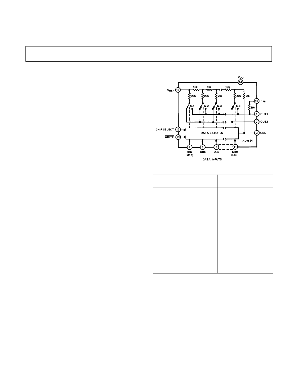
The AD7524 is a low cost, 8-bit monolithic CMOS DAC
designed for direct interface to most microprocessors.
Basically an 8-bit DAC with input latches, the AD7524’s load
cycle is similar to the “write” cycle of a random access
memory. Using an advanced thin-film on CMOS fabrication
process, the AD7524 provides accuracy to 1/8 LSB with a typical power dissipation of less than 10 milliwatts.
A newly improved design eliminates the protection Schottky
previously required and guarantees TTL compatibility when
using a +5 V supply. Loading speed has been increased for
compatibility with most microprocessors.
Featuring operation from +5 V to +15 V, the AD7524 interfaces directly to most microprocessor buses or output ports.
Excellent multiplying characteristics (2- or 4-quadrant) make
the AD7524 an ideal choice for many microprocessor controlled gain setting and signal control applications.
8-Bit Buffered Multiplying DAC
AD7524
FUNCTIONAL BLOCK DIAGRAM
ORDERING GUIDE
1
Model
AD7524JN –40°C to +85°C ±1/2 LSB N-16
AD7524KN –40°C to +85°C ±1/4 LSB N-16
AD7524LN –40°C to +85°C ±1/8 LSB N-16
AD7524JP –40°C to +85°C ±1/2 LSB P-20A
AD7524KP –40°C to +85°C ±1/4 LSB P-20A
AD7524LP –40°C to +85°C ±1/8 LSB P-20A
AD7524JR –40°C to +85°C ±1/2 LSB R-16A
AD7524AQ –40°C to +85°C ± 1/2 LSB Q-16
AD7524BQ –40°C to +85°C ±1/4 LSB Q-16
AD7524CQ –40°C to +85°C ±1/8 LSB Q-16
AD7524SQ –55°C to +125°C ±1/2 LSB Q-16
AD7524TQ –55°C to +125°C ±1/4 LSB Q-16
AD7524UQ –55°C to +125°C ±1/8 LSB Q-16
AD7524SE –55°C to +125°C ±1/2 LSB E-20A
AD7524TE –55°C to +125°C ±1/4 LSB E-20A
AD7524UE –55°C to +125°C ±1/8 LSB E-20A
NOTES
1
To order MIL-STD-883, Class B processed parts, add/883B to part number.
Contact your local sales office for military data sheet. For U.S. Standard
Military Drawing (SMD) see DESC drawing #5962-87700.
2
E = Leadless Ceramic Chip Carrier: N = Plastic DIP; P = Plastic Leaded Chip
Carrier; Q = Cerdip; R = SOIC.
Temperature Nonlinearity Package
Range (VDD = +15 V) Option
2
REV. B
Information furnished by Analog Devices is believed to be accurate and
reliable. However, no responsibility is assumed by Analog Devices for its
use, nor for any infringements of patents or other rights of third parties
which may result from its use. No license is granted by implication or
otherwise under any patent or patent rights of Analog Devices.
One Technology Way, P.O. Box 9106, Norwood, MA 02062-9106, U.S.A.
Tel: 617/329-4700 Fax: 617/326-8703
(V
= +10 V, V
AD7524–SPECIFICA TIONS
REF
Limit, TA = +258C Limit, T
Parameter VDD = +5 V VDD = +15 V VDD = 5 V VDD = +15 V Units Test Conditions/Comments
OUT1
MIN
= V
= 0 V, unless otherwise noted)
OUT2
1
, T
MAX
STATIC PERFORMANCE
Resolution 8 8 8 8 Bits
Relative Accuracy
J, A, S Versions ±1/2 ± 1/2 ±1/2 ±1/2 LSB max
K, B, T Versions ±1/2 ± 1/4 ±1/2 ±1/4 LSB max
L, C, U Versions ±1/2 ± 1/8 ±1/2 ±1/8 LSB max
Monotonicity Guaranteed Guaranteed Guaranteed Guaranteed
Gain Error
Average Gain TC
DC Supply Rejection,3 ∆Gain/∆VDD0.08 0.02 0.16 0.04 % FSR/% max ∆VDD = ±10%
2
3
± 2 1/2 ±1 1/4 ±3 1/2 ±1 1/2 LSB max
± 40 ± 10 ±40 ±10 ppm/°C Gain TC Measured from +25°C to
T
or from +25°C to T
MIN
MAX
0.002 0.001 0.01 0.005 % FSR/% typ
Output Leakage Current
I
(Pin 1) ±50 ±50 ±400 ±200 nA max DB0–DB7 = 0 V; WR, CS = 0 V; V
OUT1
I
(Pin 2) ±50 ±50 ±400 ±200 nA max DB0–DB7 = VDD; WR, CS = 0 V; V
OUT2
DYNAMIC PERFORMANCE
Output Current Settling Time
(to 1/2 LSB) 400 250 500 350 ns max OUT1 Load = 100 Ω, C
AC Feedthrough
3
at OUT1 0.25 0.25 0.5 0.5 % FSR max V
at OUT2 0.25 0.25 0.5 0.5 % FSR max 0 V; WR, CS = 0 V
REFERENCE INPUT
RIN (Pin 15 to GND)
3
= 13 pF; WR, CS =
0 V; DB0–DB7 = 0 V to VDD to 0 V.
= ±10 V, 100 kHz Sine Wave; DB0–DB7 =
REF
4
5555 kΩ min
EXT
20 20 20 20 kΩ max
ANALOG OUTPUTS
Output Capacitance
C
(Pin 1) 120 120 120 120 pF max DB0–DB7 = VDD; WR, CS = 0 V
OUT1
C
(Pin 2) 30 30 30 30 pF max
OUT2
C
(Pin 1) 30 30 30 30 pF max DB0–DB7 = 0 V; WR, CS = 0 V
OUT1
C
(Pin 2) 120 120 120 120 pF max
OUT2
3
DIGITAL INPUTS
Input HIGH Voltage Requirement
V
IH
Input LOW Voltage Requirement
V
IL
Input Current
I
IN
Input Capacitance
3
+2.4 +13.5 +2.4 +13.5 V min
+0.8 +1.5 +0.5 +1.5 V max
±1 ±1 ±10 ±10 µA max VIN = 0 V or V
DD
DB0–DB7 5 5 5 5 pF max VIN = 0 V
WR, CS 20 20 20 20 pF max VIN = 0 V
SWITCHING CHARACTERISTICS
Chip Select to Write Setup Time
t
CS
AD7524J, K, L, A, B, C 170 100 220 130 ns min
5
See Timing Diagram
tWR = t
CS
AD7524S, T, U 170 100 240 150 ns min
Chip Select to Write Hold Time
t
CH
All Grades 0 0 0 0 ns min
Write Pulse Width
t
WR
AD7524J, K, L, A, B, C 170 100 220 130 ns min
tCS ≥ tWR, tCH ≥ 0
AD7524S, T, U 170 100 240 150 ns min
Data Setup Time
t
DS
AD7524J, K, L, A, B, C 135 60 170 80 ns min
AD7524S, T, U 135 60 170 100 ns min
Data Hold Time
t
DH
All Grades 10 10 10 10 ns min
POWER SUPPLY
I
DD
NOTES
1
Temperature ranges as follows: J, K, L versions: –40 °C to +85°C
2
Gain error is measured using internal feedback resistor. Full-Scale Range (FSR) = V
3
Guaranteed not tested.
4
DAC thin-film resistor temperature coefficient is approximately –300 ppm/°C.
5
AC parameter, sample tested @ +25°C to ensure conformance to specification.
Specifications subje
ct to change without notice
A, B, C versions: –40°C to +85°C
S, T, U versions: –55°C to +125°C
1 2 2 2 mA max All Digital Inputs VIL or V
100 100 500 500 µA max All Digital Inputs 0 V or V
.
REF
.
IH
DD
= ±10 V
REF
REF
= ±10 V
–2–
REV. B
AD7524
ABSOLUTE MAXIMUM RATINGS*
(TA = +25°C, unless otherwise noted)
VDD to GND . . . . . . . . . . . . . . . . . . . . . . . . . . .–0.3 V, +17 V
V
to GND . . . . . . . . . . . . . . . . . . . . . . . . . . . . . . . . . ±25 V
RFB
V
to GND . . . . . . . . . . . . . . . . . . . . . . . . . . . . . . . . . ±25 V
REF
Digital Input Voltage to GND . . . . . . . . –0.3 V to V
OUT1, OUT2 to GND . . . . . . . . . . . . . –0.3 V to V
*Stresses above those listed under “Absolute Maximum Ratings” may cause
permanent damage to the device. This is a stress rating only and functional
operation of the device at these or any other conditions above those indicated in the
operational sections of this specification is not implied. Exposure to absolute
maximum rating conditions for extended periods may affect device reliability.
CAUTION
ESD (electrostatic discharge) sensitive device. Electrostatic charges as high as 4000 V readily
accumulate on the human body and test equipment and can discharge without detection.
Although the AD7524 features proprietary ESD protection circuitry, permanent damage may
occur on devices subjected to high energy electrostatic discharges. Therefore, proper ESD
precautions are recommended to avoid performance degradation or loss of functionality.
+0.3 V
DD
+0.3 V
DD
TERMINOLOGY
RELATIVE ACCURACY: A measure of the deviation from a
straight line through the end points of the DAC transfer function.
Normally expressed as a percentage of full scale range. For the
AD7524 DAC, this holds true over the entire V
RESOLUTION: Value of the LSB. For example, a unipolar converter with n bits has a resolution of (2 verter of n bits has a resolution of [2
–n
–(n–1)
) (V
] [V
range.
REF
). A bipolar con-
REF
]. Resolution in no
REF
way implies linearity. GAIN ERROR: Gain Error is a measure of the output error be-
tween an ideal DAC and the actual device output. It is measured
Power Dissipation (Any Package)
To +75°C . . . . . . . . . . . . . . . . . . . . . . . . . . . . . . . . 450 mW
Derates above 75°C by . . . . . . . . . . . . . . . . . . . . 6 mW/°C
Operating Temperature
Commercial (J, K, L) . . . . . . . . . . . . . . . . . –40°C to +85°C
Industrial (A, B, C) . . . . . . . . . . . . . . . . . . –40°C to +85°C
Extended (S, T, U) . . . . . . . . . . . . . . . . . –55°C to +125°C
Storage Temperature . . . . . . . . . . . . . . . . . . –65°C to +150°C
Lead Temperature (Soldering, 10 secs) . . . . . . . . . . . +300°C
with all 1s in the DAC after offset error has been adjusted out
and is expressed in LSBs. Gain Error is adjustable to zero with
an external potentiometer.
FEEDTHROUGH ERROR: Error caused by capacitive coupling from V
to output with all switches OFF.
REF
OUTPUT CAPACITANCE: Capacity from OUT1 and OUT2 terminals to ground.
OUTPUT LEAKAGE CURRENT: Current which appears on OUT1 terminal with all digital inputs LOW or on OUT2 terminal when all inputs are HIGH. This is an error current which contributes an offset voltage at the amplifier output.
WARNING!
ESD SENSITIVE DEVICE
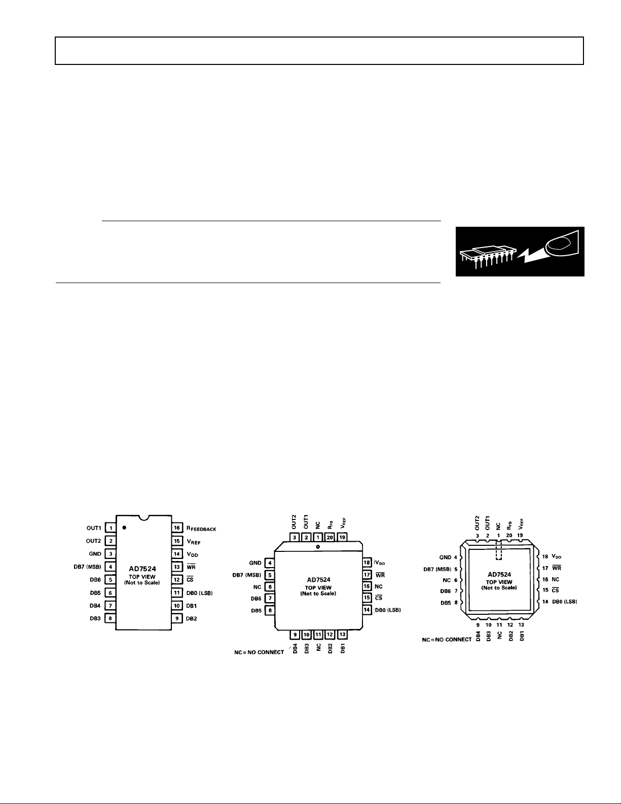
PIN CONFIGURATIONS
DIP, SOIC PLCC
LCCC
REV. B
–3–

AD7524
CIRCUIT DESCRIPTION
CIRCUIT INFORMATION
The AD7524, an 8-bit multiplying D/A converter, consists of a
highly stable thin film R-2R ladder and eight N-channel current
switches on a monolithic chip. Most applications require the
addition of only an output operational amplifier and a voltage
or current reference.
The simplified D/A circuit is shown in Figure 1. An inverted
R-2R ladder structure is used—that is, the binarily weighted
currents are switched between the OUT1 and OUT2 bus lines,
thus maintaining a constant current in each ladder leg independent of the switch state.
WRITE MODE
When CS and WR are both LOW, the AD7524 is in the
WRITE mode, and the AD7524 analog output responds to data
activity at the DB0–DB7 data bus inputs. In this mode, the
AD7524 acts like a nonlatched input D/A converter.
HOLD MODE
When either CS or WR is HIGH, the AD7524 is in the HOLD
mode. The AD7524 analog output holds the value corresponding to the last digital input present at DB0–DB7 prior to
WR or
CS assuming the HIGH state.
MODE SELECTION TABLE
CS WR Mode DAC Response
L L Write DAC responds to data bus
(DB0–DB7) inputs.
H X Hold Data bus (DB0–DB7) is
Locked Out:
X H Hold DAC holds last data present
when
WR or CS assumed
HIGH state.
L = Low State, H = High State, X = Don't Care.
WRITE CYCLE TIMING DIAGRAM
Figure 1. Functional Diagram
EQUIVALENT CIRCUIT ANALYSIS
The equivalent circuit for all digital inputs LOW is shown in
Figures 2. In Figure 2 with all digital inputs LOW, the reference current is switched to OUT2. The current source I
LEAKAGE
is composed of surface and junction leakages to the substrate
while the
1
current source represents a constant 1-bit cur-
256
rent drain through the termination resistor on the R-2R ladder.
The “ON” capacitance of the output N-channel switches is
120 pF, as shown on the OUT2 terminal. The “OFF” switch
capacitance is 30 pF, as shown on the OUT1 terminal. Analysis
of the circuit for all digital inputs high is similar to Figure 2
however, the “ON” switches are now on terminal OUT1, hence
the 120 pF appears at that terminal.
Figure 2. AD7524 DAC Equivalent Circuit—All Digital
Inputs Low
INTERFACE LOGIC INFORMATION
MODE SELECTION
AD7524 mode selection is controlled by the CS and WR inputs.
Figure 3. Supply Current vs. Logic Level
Typical plots of supply current, IDD, versus logic input voltage,
V
, for VDD = +5 V and VDD = +15 V are shown above.
IN
–4–
REV. B

ANALOG CIRCUIT CONNECTIONS
AD7524
AD7524
Figure 4. Unipolar Binary Operation
(2-Quadrant Multiplication)
Table I. Unipolar Binary Code Table
Digital Input
MSB LSB Analog Output
1111 1111 –V
1000 0001 –V
1000 0000 –V
0111 1111 –V
0000 0001 –V
0000 0000 –V
Note: 1 LSB = (2–8)(V
) = 1/256 (V
REF
(255/256)
REF
(129/256)
REF
(128/256) = –V
REF
(127/256)
REF
(1/256)
REF
(0/256) = 0
REF
)
REF
MICROPROCESSOR INTERFACE
REF
AD7524
Figure 5. Bipolar (4-Quadrant) Operation
Table II. Bipolar (Offset Binary) Code Table
Digital Input
MSB LSB Analog Output
1111 1111 +V
1000 0001 +V
/2
1000 0000 0
0111 1111 –V
0000 0001 –V
0000 0000 –V
Note: 1 LSB = (2–7)(V
) = 1/128 (V
REF
REF
)
(127/128)
REF
(1/128 )
REF
(1/128)
REF
(127/128)
REF
(128/128)
REF
REV. B
Figure 6. AD7524/8085A Interface
Figure 7. AD7524/MC6800 Interface
–5–

AD7524
POWER GENERATION
Figure 8.
–6–
REV. B

OUTLINE DIMENSIONS
3
PIN 1
IDENTIFIER
4
19
18
8
9
14
13
TOP VIEW
(PINS DOWN)
0.395 (10.02)
0.385 (9.78)
SQ
0.356 (9.04)
0.350 (8.89)
SQ
0.048 (1.21)
0.042 (1.07)
0.048 (1.21)
0.042 (1.07)
0.020
(0.50)
R
0.050
(1.27)
BSC
0.021 (0.53)
0.013 (0.33)
0.330 (8.38)
0.290 (7.37)
0.032 (0.81)
0.026 (0.66)
0.180 (4.57)
0.165 (4.19)
0.040 (1.01)
0.025 (0.64)
0.056 (1.42)
0.042 (1.07)
0.025 (0.63)
0.015 (0.38)
0.110 (2.79)
0.085 (2.16)
Dimensions shown in inches and (mm).
AD7524
20-Terminal Ceramic Leadless Chip Carrier
(E-20A)
0.200 (5.08)
BSC
REF
0.055 (1.40)
0.045 (1.14)
0.075
(1.91)
REF
19
18
14
13
20
1
BOTTOM
VIEW
0.150 (3.81)
BSC
0.358 (9.09)
0.342 (8.69)
SQ
0.100 (2.54)
0.064 (1.63)
0.358
(9.09)
MAX
SQ
0.088 (2.24)
0.054 (1.37)
0.095 (2.41)
0.075 (1.90)
0.011 (0.28)
0.007 (0.18)
R TYP
0.075 (1.91)
16-Lead Plastic DIP (Narrow)
(N-16)
0.840 (21.33)
0.745 (18.93)
0.210 (5.33)
MAX
0.160 (4.06)
0.115 (2.93)
16
18
PIN 1
0.022 (0.558)
0.014 (0.356)
0.100
(2.54)
BSC
9
0.280 (7.11)
0.240 (6.10)
0.060 (1.52)
0.015 (0.38)
0.130
(3.30)
MIN
0.070 (1.77)
0.045 (1.15)
SEATING
PLANE
0.100 (2.54) BSC
0.015 (0.38)
3
MIN
4
0.028 (0.71)
0.022 (0.56)
0.050 (1.27)
8
BSC
9
45° TYP
0.325 (8.25)
0.300 (7.62)
0.015 (0.381)
0.008 (0.204)
0.195 (4.95)
0.115 (2.93)
20-Lead Plastic Leadless Chip Carrier (PLCC)
(P-20A)
16-Lead Cerdip
(Q-16)
0.005 (0.13) MIN
0.200 (5.08)
MAX
0.200 (5.08)
0.125 (3.18)
16
1
PIN 1
0.840 (21.34) MAX
0.023 (0.58)
0.014 (0.36)
0.100
(2.54)
BSC
0.080 (2.03) MAX
9
0.310 (7.87)
0.220 (5.59)
8
0.060 (1.52)
0.015 (0.38)
0.070 (1.78)
0.030 (0.76)
0.150
(3.81)
MIN
SEATING
PLANE
0.320 (8.13)
0.290 (7.37)
15°
0°
0.015 (0.38)
0.008 (0.20)
REV. B
0.1574 (4.00)
0.1497 (5.80)
0.0098 (0.25)
0.0040 (0.10)
SEATING
PLANE
16-Lead Narrow-Body (SOIC)
(R-16A)
0.3937 (10.00)
0.3859 (9.80)
16 9
PIN 1
0.0500
0.0192 (0.49)
(1.27)
0.0138 (0.35)
BSC
0.2550 (6.20)
81
0.2284 (5.80)
0.0688 (1.75)
0.0532 (1.35)
0.0099 (0.25)
0.0075 (0.19)
0.0196 (0.50)
0.0099 (0.25)
8°
0°
–7–
x 45°
0.0500 (1.27)
0.0160 (0.41)

C542e–5–11/86
–8–
PRINTED IN U.S.A.
 Loading...