CMOS, 8-Bit,
V
Enhanced Product
FEATURES
Microprocessor compatible (6800, 8085, Z80)
TTL-/CMOS-compatible inputs
On-chip data latches
Endpoint linearity
Low power consumption
Monotonicity guaranteed (full temperature range)
Latch free (no protection Schottky required)
ENHANCED PRODUCT FEATURES
Supports defense and aerospace applications (AQEC)
Military temperature range (−55°C to +125°C)
Controlled manufacturing baseline
One assembly/test site
One fabrication site
Enhanced product change notification
Qualification data available on request
CHIP SELECT
WRITE
Buffered Multiplying DAC
AD7524-EP
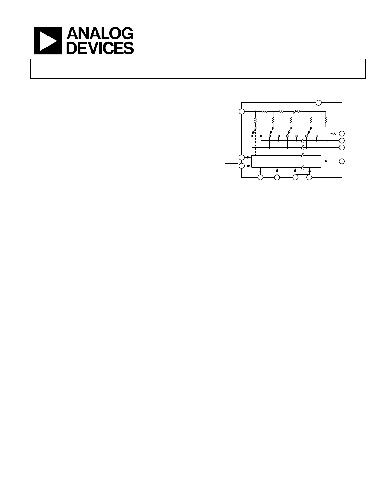
FUNCTIONAL BLOCK DIAGRAM
DD
10kΩ
10kΩ
S2
5
Figure 1.
10kΩ
20kΩ
S3
DB5
15
V
REF
20kΩ
20kΩ
S1
12
13
4
DB7
(MSB)
DATA LATCHES
DB6
DATA INPUTS
14
20kΩS820kΩ
AD7524-EP
36
DB0
(LSB)
10kΩ
16
1
2
3
R
FB
OUT1
OUT2
GND
01132-001
APPLICATIONS
Microprocessor controlled gain circuits
Microprocessor controlled attenuator circuits
Microprocessor controlled function generation
Precision AGC circuits
Bus structured instruments
GENERAL DESCRIPTION
The AD7524-EP is a low cost, 8-bit monolithic CMOS DAC
designed for direct interface to most microprocessors.
An 8-bit DAC with input latches, the load cycle of the AD7524-EP
is similar to the write cycle of the random access memory. Using
an advanced thin-film on the CMOS fabrication process, the
AD7524-EP provides accuracy to ⅛ LSB with a typical power
dissipation of less than 10 mW.
An improved design eliminates the protection Schottky previously
required and guarantees TTL compatibility when using a 5 V
supply. The loading speed has also been increased for compatibility
with most microprocessors.
Featuring operation from 5 V to 15 V, the AD7524-EP interfaces
directly to most microprocessor buses or output ports.
Excellent multiplying characteristics (2- or 4-quadrant) make
the AD7524-EP an ideal choice for many microprocessor
controlled gain setting and signal control applications.
Additional application and technical information can be found
in the AD7524 data sheet.
Rev. 0
Information furnished by Analog Devices is believed to be accurate and reliable. However, no
responsibility is assumed by Anal og Devices for its use, nor for any infringements of patents or ot her
rights of third parties that may result from its use. Specifications subject to change without notice. No
license is granted by implication or otherwise under any patent or patent rights of Analog Devices.
Trademarks and registered trademarks are the property of their respective owners.
One Technology Way, P.O. Box 9106, Norwood, MA 02062-9106, U.S.A.
Tel: 781.329.4700 www.analog.com
Fax: 781.461.3113 ©2012 Analog Devices, Inc. All rights reserved.

AD7524-EP Enhanced Product
TABLE OF CONTENTS
Features.............................................................................................. 1
Enhanced Product Features ............................................................ 1
Applications....................................................................................... 1
Functional Block Diagram .............................................................. 1
General Description ......................................................................... 1
Revision History ............................................................................... 2
Specifications..................................................................................... 3
REVISION HISTORY
1/12—Revision 0: Initial Version
Write Cycle Timing Diagram ......................................................4
Absolute Maximum Ratings ............................................................5
ESD Caution...................................................................................5
Pin Configuration and Function Descriptions..............................6
Outline Dimensions..........................................................................7
Ordering Guide .............................................................................7
Rev. 0 | Page 2 of 8

Enhanced Product AD7524-EP
SPECIFICATIONS
V
= 10 V, V
REF
OUT1
= V
= 0 V, unless otherwise noted. Temperature range goes from −55°C to +125°C.
OUT2
Table 1.
Limit, TA = 25°C Limit, T
MIN
1
, T
Test Conditions/
MAX
Parameter VDD = 5 V VDD = 15 V VDD = 5 V VDD = 15 V Unit Comments
STATIC PERFORMANCE
Resolution 8 8 8 8 Bits
Relative Accuracy ±1/2 ±1/2 ±1/2 ±1/2 LSB max
Monotonicity Guaranteed Guaranteed Guaranteed Guaranteed
Gain Error2 ±2½ ±1¼ ±3½ ±1½ LSB max
Average Gain TC3 ±40 ±10 ±40 ±10 ppm/°C
DC Supply Rejection, ΔGain/ΔV
3
0.08 0.02 0.16 0.04
DD
% FSR/%
Gain TC measured from
= ±10%
DD
or from
MIN
MAX
25°C to T
25°C to T
ΔV
max
0.002 0.001 0.01 0.005 % FSR/% typ
Output Leakage Current
I
(Pin 1) ±50 ±50 ±400 ±200 nA max
OUT1
I
(Pin 2) ±50 ±50 ±400 ±200 nA max
OUT2
DB0 to DB7 = 0 V;WR
CS
= 0 V; V
= ±10 V
REF
DB0 to DB7 = V
CS = 0 V; V
= ±10 V
REF
DYNAMIC PERFORMANCE
Output Current Settling Time
(to ½ LSB)
3
400 250 500 350 ns max
OUT1 load = 100 Ω,
= 13 pF; WR, CS = 0 V;
C
EXT
DB0 to DB7 = 0 V to
V
to 0 V
DD
AC Feedthrough3
At OUT1 0.25 0.25 0.5 0.5 % FSR max
= ±10 V, 100 kHz sine
V
REF
wave; DB0 to DB7 = 0 V;
WR, CS = 0 V
At OUT2 0.25 0.25 0.5 0.5 % FSR max
= ±10 V, 100 kHz sine
V
REF
wave; DB0 to DB7 = 0 V;
WR, CS = 0 V
REFERENCE INPUT
RIN (Pin 15 to GND)4 5 5 5 5 kΩ min
20 20 20 20 kΩ max
ANALOG OUTPUTS
Output Capacitance3
C
(Pin 1) 120 120 120 120 pF max
OUT1
C
(Pin 2) 30 30 30 30 pF max
OUT2
C
(Pin 1) 30 30 30 30 pF max
OUT1
C
(Pin 2) 120 120 120 120 pF max
OUT2
DB0 to DB7 = V
, CS = 0 V
WR
DB0 to DB7 = 0 V;
, CS = 0 V
WR
DIGITAL INPUTS
Input High Voltage Requirement, VIH 2.4 13.5 2.4 13.5 V min
Input Low Voltage Requirement, VIL 0.8 1.5 0.5 1.5 V max
Input Current, IIN ±1 ±1 ±10 ±10 μA max VIN = 0 V or VDD
Input Capacitance3
DB0 to DB7 5 5 5 5 pF max VIN = 0 V
WR, CS
20 20 20 20 pF max V
= 0 V
IN
DD
DD
,
; WR,
;
Rev. 0 | Page 3 of 8
 Loading...