+3 V/+5 V, Dual,
VDDV
FEATURES
Micropower: 100 μA/DAC
0.1 μA typical power shutdown
Single-supply 2.7 V to 5.5 V operation
12-bit resolution
Serial interface with Schmitt trigger inputs
APPLICATIONS
Automotive output span voltage
Portable communications
Digitally controlled calibration
PC peripherals
CLK
SDI
(DATA)
LDA
LDB
CS
Serial Input 12-Bit DAC
AD7394
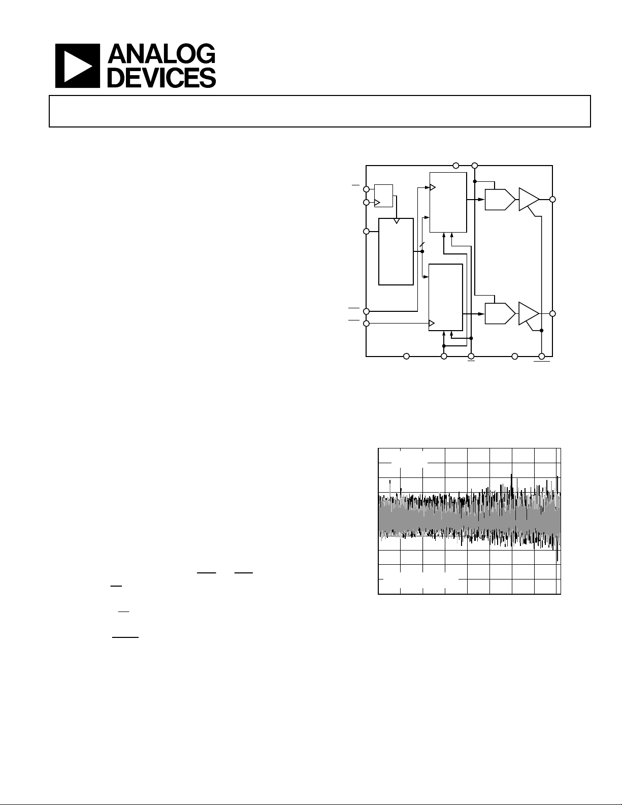
FUNCTIONAL BLOCK DIAGRAM
REF
OP AMP
AGND
A
OP AMP
B
SHDN
EN
SHIFT
REGISTER
DGND MSB
DAC A
REGISTER
D
PR
12
D
DAC B
REGISTER
PR
DAC A
AD7394
DAC B
RS
Figure 1.
V
V
OUTA
OUTB
08528-001
GENERAL DESCRIPTION
The AD7394 is dual, 12-bit, voltage output digital-to-analog
converter designed to operate from a single 3 V supply. Built
using a CBCMOS process, this monolithic DAC offers the
user low cost and ease-of-use in a single-supply 3 V system.
Operation is guaranteed over the supply voltage range of 2.7 V
to 5.5 V making this device ideal for battery-operated
applications.
The full-scale output voltage is determined by the applied
external reference input voltage, V
input to V
to the positive supply, V
outputs allows for a full-scale voltage set equal
OUT
, or any value in between.
DD
A doubled-buffered serial data interface offers high speed,
microcontroller compatible inputs using the serial-data-in
(SDI), clock (CLK), and load strobe (
CS
A chip-select (
) pin simplifies the connection of multiple
DAC packages by enabling the clock input when active low.
Additionally, an
RS
input sets the output to zero scale or to 1/2
scale based on the logic level applied to the MSB pin. The power
SHDN
shutdown pin,
, reduces power dissipation to nanoamp
current levels. All digital inputs contain Schmitt-triggered logic
levels to minimize power dissipation and prevent false
triggering on the clock input.
. The rail-to-rail V
REF
LDA
and
LDB
REF
) pins.
The AD7394 is specified over the extended industrial (−40°C
to +85°C) temperature range and is available in a low profile
1.75 mm height SOIC surface mount package.
1.0
VDD = 3V
0.8
0.6
0.4
0.2
0
DNL (LSB)
–0.2
–0.4
–0.6
–0.8
–1.0
= 2.5V
V
REF
TA = –55°C, +25°C, +85°C
SUPERIMPOSED
0 500 1000 1500 2000 2500 3000 3500 4000
CODE (Decimal)
Figure 2. Differential Nonlinearity Error vs. Code
08528-002
Rev. A
Information furnished by Analog Devices is believed to be accurate and reliable. However, no
responsibility is assumed by Analog Devices for its use, nor for any infringements of patents or other
rights of third parties that may result from its use. Specifications subject to change without notice. No
license is granted by implication or otherwise under any patent or patent rights of Analog Devices.
Trademarks and registered trademarks are the property of their respective owners.
One Technology Way, P.O. Box 9106, Norwood, MA 02062-9106, U.S.A.
Tel: 781.329.4700 www.analog.com
Fax: 781.461.3113 ©1998–2010 Analog Devices, Inc. All rights reserved.

AD7394
TABLE OF CONTENTS
Features .............................................................................................. 1
Applications ....................................................................................... 1
Functional Block Diagram .............................................................. 1
General Description ......................................................................... 1
Revision History ............................................................................... 2
Specifications ..................................................................................... 3
AD7394 Electrical Characteristics ............................................. 3
Absolute Maximum Ratings ............................................................ 7
ESD Caution .................................................................................. 7
Pin Configuration and Function Descriptions ............................. 8
Typical Performance Characteristics ............................................. 9
Theory of Operation ...................................................................... 12
REVISION HISTORY
1/10—Rev. 0 to Rev. A
Updated Format .................................................................. Universal
Removed AD7395 ............................................................... Universal
Updated Outline Dimensions ....................................................... 18
Changes to Ordering Guide .......................................................... 19
4/98—Revision. 0: Initial Version
DAC Section ................................................................................ 12
Amplifier Section ....................................................................... 12
Reference Input ........................................................................... 12
Power Supply ............................................................................... 13
Power Supply Bypassing And Grounding ............................... 13
Input Logic Levels ...................................................................... 13
Digital Interface .......................................................................... 14
Reset (RS) Pin ............................................................................. 14
Power Shutdown (
Unipolar Output Operation ...................................................... 15
Outline Dimensions ....................................................................... 16
Ordering Guide .......................................................................... 16
SHDN
) ......................................................... 15
Rev. A | Page 2 of 16

AD7394
SPECIFICATIONS
AD7394 ELECTRICAL CHARACTERISTICS
@ V
Table 1.
Parameter Symbol Conditions 3 V ± 10% 5 V ± 10% Unit
STATIC PERFORMANCE
REFERENCE INPUT
ANALOG OUTPUT
LOGIC INPUTS
INTERFACE TIMING
AC CHARACTERISTICS
Data = 000H, f = 100 kHz −63 −63 dB typ
= 2.5 V, −40°C < TA < +85°C, unless otherwise noted.
REF IN
Resolution1 N 12 12 Bits
Relative Accuracy2 INL TA = +25°C ±1.5 ±1.5 LSB max
T
= –40°C, +85°C ±2.0 ±2.0 LSB max
A
Differential Nonlinearity2 DNL TA = +25°C, monotonic ±0.9 ±0.9 LSB max
Monotonic ±1 ±1 LSB max
Zero-Scale Error V
Full-Scale Voltage Error V
T
Full-Scale Tempco3 TCV
V
Range V
REF IN
Input Resistance R
Input Capacitance3 C
Output Current (Source) I
Output Current (Sink) I
Data = 000H 4.0 4.0 mV max
ZSE
TA = +25°C, +85°C, data = FFFH ±8 ±8 mV max
FSE
= −40°C, data = FFFH ±20 ±20 mV max
A
−30 −30 ppm/°C typ
FS
0/VDD 0/VDD V min/max
REF
2.5 2.5 MΩ typ4
REF
5 5 pF typ
REF
Data = 800H, ΔV
OUT
Data = 800H, ΔV
OUT
= 5 LSB 1 1 mA typ
OUT
= 5 LSB 3 3 mA typ
OUT
Capacitive Load3 CL No oscillation 100 100 pF typ
Logic Input Low Voltage VIL 0.5 0.8 V max
Logic Input High Voltage V
V
IH
− 0.6 4.0 V min
DD
Input Leakage Current IIL 10 10 μA max
Input Capacitance3 C
3, 5
10 10 pF max
IL
Clock Width High tCH 50 30 ns min
Clock Width Low tCL 50 30 ns min
Load Pulsewidth t
30 20 ns min
LDW
Data Setup tDS 10 10 ns min
Data Hold tDH 30 15 ns min
Clear Pulsewidth t
Load Setup t
Load Hold t
15 15 ns min
CLRW
30 15 ns min
LD1
40 20 ns min
LD2
Output Slew Rate SR Data = 000H to FFFH to 000H 0.05 0.05 V/μs typ
Settling Time6 t
To ±0.1% of full scale 70 60 μs typ
S
DAC Glitch Q Code 7FFH to 800H to 7FFH 65 65 nV/s typ
Digital Feedthrough Q
Feedthrough V
V
OUT/VREF
= 1.5 VDC +1 V p-p, 15 15 nV/s typ
REF
Rev. A | Page 3 of 16

AD7394
Parameter Symbol Conditions 3 V ± 10% 5 V ± 10% Unit
SUPPLY CHARACTERISTICS
Power Supply Range V
Shutdown Supply Current
Positive Supply Current IDD VIL = 0 V, no load 125/200 125/200 μA typ/max
Power Dissipation P
Power Supply Sensitivity PSS ΔVDD = ±5% 0.006 0.006 %/% max
1
One LSB = V
2
The first two codes (000H, 001H) are excluded from the linearity error measurement.
3
These parameters are guaranteed by design and not subject to production testing.
4
Typicals represent average readings measured at 25°C.
5
All input control signals are specified with tR = tF = 2 ns (10% to 90% of +3 V) and timed from a voltage level of 1.6 V.
6
The settling time specification does not apply for negative going transitions within the last three LSBs of ground.
/4096 V for the 12-bit AD7394.
REF
DNL < ± 1 LSB 2.7/5.5 2.7/5.5 V min/max
DD RANGE
SHDN
I
DD_SD
VIL = 0 V, no load 600 1000 μW max
DISS
= 0, VIL = 0 V, no load
0.1/1.5 0.1/1.5 μA typ/max
Rev. A | Page 4 of 16

AD7394
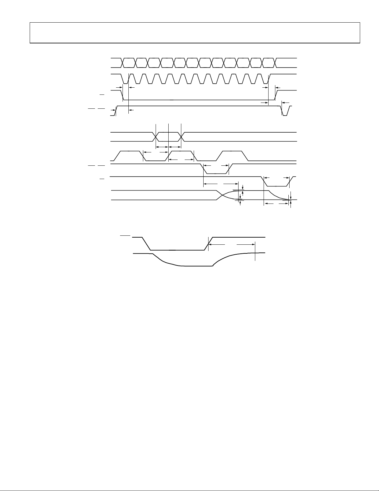
Timing Diagrams
SDI
CLK
t
CSS
CS
LDA, LDB
SDI
CLK
LDA, LDB
RS
V
OUT
t
LD1
tDSt
DH
t
CL
t
CH
FS
ZS
t
LDW
t
S
ERROR BAND
±1 LSB
Figure 3.
SHDN
I
DD
Figure 4.
t
SDR
D0D1D2D3D4D5D6D7D8D9D10D11
t
CSH
t
LD2
t
CLRW
t
S
08528-003
08528-004
Rev. A | Page 5 of 16
 Loading...