Analog Devices AD7392AR, AD7392AN, AD7393ARU, AD7393AR, AD7393AN Datasheet

+3 V, Parallel Input
12
12
12-BIT
DAC
DAC REGISTER
V
REF
SHDN
AGND
RS
DB0–DB11
CS
DGND
AD7392
V
DD
V
OUT
CODE – Decimal
1024128 256 384 512 640 768 8960
AD7393
VDD = +2.7V
V
REF
= +2.5V
TA = 258C
1
21
0.4
20.2
20.4
20.6
20.8
0.2
0
0.8
0.6
DNL – LSB
a
FEATURES
Micropower: 100 A
0.1 A Typical Power Shutdown
Single-Supply +2.7 V to +5.5 V Operation
Compact 1.1 mm Height TSSOP-20 Package
AD7392/12-Bit Resolution
AD7393/10-Bit Resolution
0.9 LSB Differential Nonlinearity Error
APPLICATIONS
Automotive 0.5 V to 4.5 V Output Span Voltage
Portable Communications
Digitally Controlled Calibration
PC Peripherals
GENERAL DESCRIPTION
The AD7392/AD7393 family of 10- and 12-bit voltage-output
digital-to-analog converters is designed to operate from a single
+3 V supply. Built using a CBCMOS process, these monolithic
DACs offer the user low cost and ease of use in single-supply
+3 V systems. Operation is guaranteed over the supply voltage
range of +2.7 V to +5.5 V, making this device ideal for battery
operated applications.
The full-scale voltage output is determined by the external
reference input voltage applied. The rail-to-rail REF
DAC
supply V
allows for a full-scale voltage set equal to the positive
OUT
or any value in between. The voltage outputs are
DD
capable of sourcing 5 mA.
A 12-bit wide data latch loads with a 45 ns write time allowing
interface to the fastest processors without wait states.
to
IN
Micropower 10- and 12-Bit DACs
AD7392/AD7393
FUNCTIONAL BLOCK DIAGRAM
Additionally, an asynchronous RS input sets the output to zero
scale at power on or upon user demand.
Both parts are offered in the same pinout to allow users to select
the amount of resolution appropriate for their applications
without circuit card changes.
The AD7392/AD7393 are specified for operation over the ex-
tended industrial (–40°C to +85°C) temperature range. The
AD7393AR is specified for the –40°C to +125°C automotive
temperature range. AD7392/AD7393s are available in plastic
DIP, and 20-lead SOIC packages. The AD7393ARU is available for ultracompact applications in a thin 1.1 mm height
TSSOP-20 package.
For serial data input, 8-lead packaged versions, see the AD7390
and AD7391 products.
1
AD7392
0.8
0.6
0.4
0.2
0
DNL – LSB
20.2
20.4
20.6
20.8
REV. A
Information furnished by Analog Devices is believed to be accurate and
reliable. However, no responsibility is assumed by Analog Devices for its
use, nor for any infringements of patents or other rights of third parties
which may result from its use. No license is granted by implication or
otherwise under any patent or patent rights of Analog Devices.
21
0 4096512
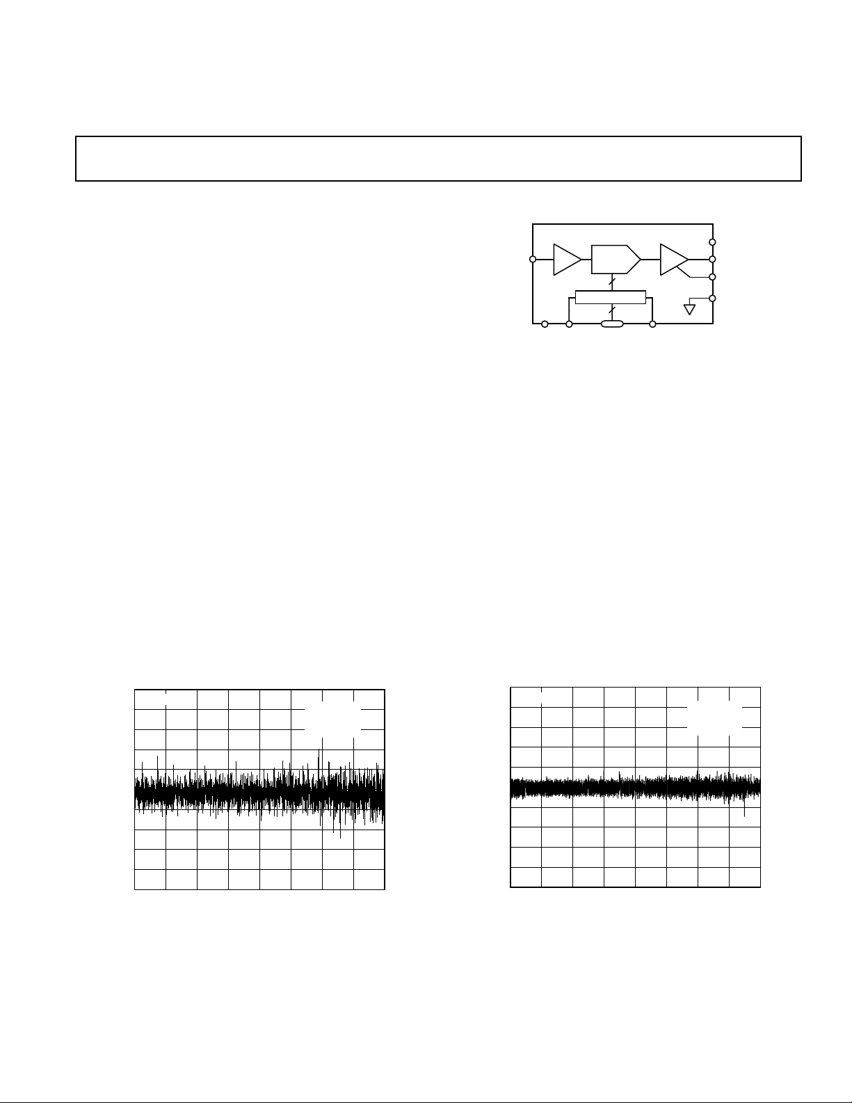
Figure 1. AD7392 Differential Nonlinearity Error vs. Code
1024 1536 2048 2560 3072 3584
CODE – Decimal
VDD = +2.7V
= +2.5V
V
REF
= 258C
T
A
Figure 2. AD7393 Differential Nonlinearity Error vs. Code
One Technology Way, P.O. Box 9106, Norwood, MA 02062-9106, U.S.A.
Tel: 781/329-4700 World Wide Web Site: http://www.analog.com
Fax: 781/326-8703 © Analog Devices, Inc., 1999

AD7392/AD7393–SPECIFICATIONS
AD7392 ELECTRICAL CHARACTERISTICS
(@ V
= 2.5 V, ⴚ40ⴗC < TA < ⴙ85ⴗC, unless otherwise noted)
REF IN
Parameter Symbol Conditions 3 V ⴞ 10% 5 V ⴞ 10% Units
STATIC PERFORMANCE
Resolution
Relative Accuracy
Differential Nonlinearity
1
2
2
N 12 12 Bits
INL T
DNL T
= ⫹25°C ⫾1.8 ⫾1.8 LSB max
A
= ⫺40°C, ⫹85°C ⫾3 ⫾3 LSB max
T
A
= ⫹25°C, Monotonic ⫾0.9 ⫾0.9 LSB max
A
Monotonic ⫾1 ⫾1 LSB max
Zero-Scale Error V
Full-Scale Voltage Error V
Full-Scale Tempco
3
ZSE
FSE
TCV
FS
Data = 000H, T
Data = 000
T
= ⫹25°C, ⫹85°C, Data = FFF
A
= ⫺40°C, Data = FFF
T
A
= ⫹25°C, ⫹85°C 4.0 4.0 mV max
A
, T
= –40°C 8.0 8.0 mV max
H
A
H
⫾8 ⫾8mV max
H
⫾20 ⫾20 mV max
28 28 ppm/°C typ
REFERENCE INPUT
V
Range V
REF IN
Input Resistance R
Input Capacitance
3
REF
REF
C
REF
0/V
DD
0/V
DD
V min/max
2.5 2.5 MΩ typ
5 5 pF typ
ANALOG OUTPUT
Current (Source) I
Output Current (Sink) I
Capacitive Load
3
OUT
OUT
C
L
Data = 800
Data = 800
H
H
, ∆V
, ∆V
= 5 LSB 1 1 mA typ
OUT
= 5 LSB 3 3 mA typ
OUT
No Oscillation 100 100 pF typ
LOGIC INPUTS
Logic Input Low Voltage V
Logic Input High Voltage V
Input Leakage Current I
Input Capacitance
INTERFACE TIMING
3
3, 5
Chip Select Write Width t
Data Setup t
Data Hold t
Reset Pulsewidth t
IL
IH
IL
C
IL
CS
DS
DH
RS
0.5 0.8 V max
VDD⫺0.6 VDD⫺0.6 V min
10 10 µA max
10 10 pF max
45 45 ns min
30 15 ns min
20 5 ns min
40 30 ns min
AC CHARACTERISTICS
Output Slew Rate SR Data = 000
Settling Time
Shutdown Recovery Time t
6
t
S
SDR
To ±0.1% of Full Scale 70 60 µs typ
DAC Glitch Q Code 7FF
to FFFH to 000
H
to 800H to 7FF
H
H
0.05 0.05 V/µs typ
80 µs typ
H
65 65 nV/s typ
Digital Feedthrough Q 15 15 nV/s typ
Feedthrough V
OUT/VREFVREF
= 1.5 V dc +1 V p-p
,
Data = 000H, f = 100 kHz –63 –63 dB typ
SUPPLY CHARACTERISTICS
Power Supply Range V
Positive Supply Current I
Shutdown Supply Current I
Power Dissipation P
DD RANGE
DD
DD–SD
DISS
Power Supply Sensitivity PSS ∆V
NOTES
1
One LSB = V
2
The first two codes (000H, 001H) are excluded from the linearity error measurement.
3
These parameters are guaranteed by design and not subject to production testing.
4
Typicals represent average readings measured at +25°C.
5
All input control signals are specified with tR = tF = 2 ns (10% to 90% of 13 V) and timed from a voltage level of 1.6 V.
6
The settling time specification does not apply for negative going transitions within the last 3 LSBs of ground.
Specifications subject to change without notice.
/4096 V for the 12-bit AD7392.
REF
DNL < ⫾1 LSB 2.7/5.5 2.7/5.5 V min/max
V
= 0 V, No Load 55/100 55/100 µA typ/max
IL
SHDN = 0, V
V
= 0 V, No Load 300 500 µW max
IL
= ⫾5% 0.006 0.006 %/% max
DD
= 0 V, No Load 0.1/1.5 0.1/1.5 µA typ/max
IL
4
–2–
REV. A

AD7392/AD7393
AD7393 ELECTRICAL CHARACTERISTICS
(@ V
= 2.5 V, ⴚ40ⴗC < TA < ⴙ85ⴗC, unless otherwise noted)
REF IN
Parameter Symbol Conditions 3 V ⴞ 10% 5 V ⴞ 10% Units
STATIC PERFORMANCE
Resolution
Relative Accuracy
Differential Nonlinearity
Zero-Scale Error V
Full-Scale Voltage Error V
Full-Scale Tempco
1
2
2
3
N 10 10 Bits
INL T
= ⫹25°C ⫾1.75 ⫾1.75 LSB max
A
= ⫺40°C, ⫹85°C, ⫹125°C ⫾2.0 ⫾2.0 LSB max
T
A
DNL Monotonic ⫾0.8 ⫾0.8 LSB max
ZSE
FSE
TCV
FS
Data = 000
T
= ⫹25°C, ⫹85°C, ⫹125°C, ⫾32 ⫾32 mV max
A
Data = 3FF
T
= ⫺40°C, Data = 3FF
A
H
H
H
9.0 9.0 mV max
⫾42 ⫾42 mV max
28 28 ppm/°C typ
REFERENCE INPUT
V
Range V
REF IN
Input Resistance R
Input Capacitance
3
REF
REF
C
REF
0/V
DD
0/V
DD
V min/max
2.5 2.5 MΩ typ
5 5 pF typ
ANALOG OUTPUT
Output Current (Source) I
Output Current (Sink) I
Capacitive Load
3
OUT
OUT
C
L
Data = 200
Data = 200
H
H
, ∆V
, ∆V
= 5 LSB 1 1 mA typ
OUT
= 5 LSB 3 3 mA typ
OUT
No Oscillation 100 100 pF typ
LOGIC INPUTS
Logic Input Low Voltage V
Logic Input High Voltage V
Input Leakage Current I
Input Capacitance
INTERFACE TIMING
3
3, 5
Chip Select Write Width t
Data Setup t
Data Hold t
Reset Pulsewidth t
IL
IH
IL
C
IL
CS
DS
DH
RS
0.5 0.8 V max
VDD⫺0.6 VDD⫺0.6 V min
10 10 µA max
10 10 pF max
45 45 ns
30 15 ns
20 5 ns
40 30 ns
AC CHARACTERISTICS
Output Slew Rate SR Data = 000
Settling Time
Shutdown Recovery Time t
6
t
S
SDR
To ⫾0.1% of Full Scale 70 60 µs typ
DAC Glitch Q Code 7FF
to 3FFH to 000
H
to 800H to 7FF
H
H
0.05 0.05 V/µs typ
80 µs typ
H
65 65 nV/s typ
Digital Feedthrough Q 15 15 nV/s typ
Feedthrough V
OUT/VREFVREF
= 1.5 V dc ⫹1 V p-p,
Data = 000H, f = 100 kHz –63 –63 dB typ
SUPPLY CHARACTERISTICS
Power Supply Range V
Positive Supply Current I
Shutdown Supply Current I
Power Dissipation P
DD RANGE
DD
DD–SD
DISS
Power Supply Sensitivity PSS ∆V
NOTES
1
One LSB = V
2
The first two codes (000H, 001H) are excluded from the linearity error measurement.
3
These parameters are guaranteed by design and not subject to production testing.
4
Typicals represent average readings measured at +25°C.
5
All input control signals are specified with tR = tF = 2 ns (10% to 90% of ⫹3 V) and timed from a voltage level of 1.6 V.
6
The settling time specification does not apply for negative going transitions within the last 3 LSBs of ground.
Specifications subject to change without notice.
/1024 V for the 10-bit AD7393.
REF
DNL < ⫾1 LSB 2.7/5.5 2.7/5.5 V min/max
VIL = 0 V, No Load, T
= 0 V, No Load 100 100 µA max
V
IL
SHDN = 0, V
V
= 0 V, No Load 300 500 µW max
IL
= ⫾5% 0.006 0.006 %/% max
DD
= 0 V, No Load 0.1/1.5 0.1/1.5 µA typ/max
IL
= ⫹25°C55 55 µA typ
A
4
REV. A
–3–

AD7392/AD7393
WARNING!
ESD SENSITIVE DEVICE
ABSOLUTE MAXIMUM RATINGS*
VDD to GND . . . . . . . . . . . . . . . . . . . . . . . . . . . .–0.3 V, +8 V
to GND . . . . . . . . . . . . . . . . . . . . . . . . . . . . –0.3 V, V
V
REF
DD
Logic Inputs to GND . . . . . . . . . . . . . . . . . . . . .–0.3 V, +8 V
to GND . . . . . . . . . . . . . . . . . . . . . –0.3 V, VDD + 0.3 V
V
OUT
Short Circuit to GND . . . . . . . . . . . . . . . . . . . . . 50 mA
I
OUT
DGND to AGND . . . . . . . . . . . . . . . . . . . . . . . . –0.3 V, +2 V
Package Power Dissipation . . . . . . . . . . . . . (T
Thermal Resistance θ
JA
max – T
J
)/θ
A
JA
20-Lead Plastic DIP Package (N-20) . . . . . . . . . . . 57°C/W
20-Lead SOIC Package (R-20) . . . . . . . . . . . . . . . . 60°C/W
20-Lead Thin-Shrink Surface Mount (RU-20) . . . 155°C/W
Maximum Junction Temperature (T
max) . . . . . . . . . . 150°C
J
Operating Temperature Range . . . . . . . . . . . –40°C to +85°C
AD7393AR . . . . . . . . . . . . . . . . . . . . . . . . . –40°C to +125°C
Storage Temperature Range . . . . . . . . . . . . –65°C to +150°C
Lead Temperature
N-20 (Soldering, 10 sec) . . . . . . . . . . . . . . . . . . . . .+300°C
R-20 (Vapor Phase, 60 sec) . . . . . . . . . . . . . . . . . . .+215°C
RU-20 (Infrared, 15 sec) . . . . . . . . . . . . . . . . . . . . .+220°C
*Stresses above those listed under Absolute Maximum Ratings may cause perma-
nent damage to the device. This is a stress rating only; functional operation of the
device at these or any other conditions above those indicated in the operational
sections of this specification is not implied. Exposure to absolute maximum rating
conditions for extended periods may affect device reliability.
CS
DB11–DB0
RS
V
OUT
1
0
1
0
1
0
FS
ZS
t
CS
t
DS
DATA VALID
t
t
DH
t
RS
60.1% FS
ERROR BAND
S
t
S
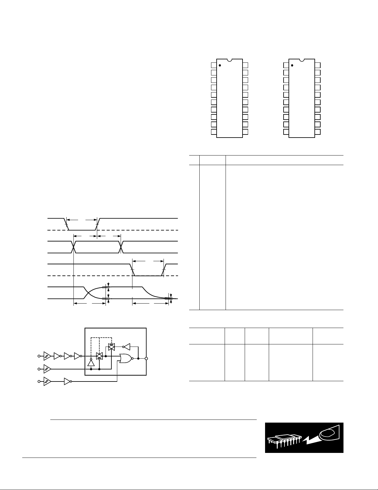
Figure 3. Timing Diagram
PIN CONFIGURATIONS
V
SHDN
CS
RS
DD
D0
D1
D2
D3
D4
D5
1
2
3
4
5
AD7392
TOP VIEW
6
(Not to Scale)
7
8
9
10
20
V
REF
19
V
OUT
18
AGND
17
DGND
16
D11
15
D10
14
D9
13
D8
12
D7
11
D6
1
V
DD
2
SHDN
CS
3
4
RS
5
NC
6
NC
7
D0
8
D1
9
D2
10
D3
NC = NO CONNECT
AD7393
TOP VIEW
(Not to Scale)
20
V
REF
19
V
OUT
18
AGND
17
DGND
16
D9
15
D8
14
D7
13
D6
12
D5
11
D4
PIN DESCRIPTION
# Name Function
1V
DD
Positive Power Supply Input. Specified range
of operation +2.7 V to +5.5 V.
2 SHDN Power Shutdown active low input. DAC regis-
ter contents are saved as long as power stays on
the V
pin. When SHDN = 0, CS strobes will
DD
write new data into the DAC register.
3 CS Chip Select latch enable, active low.
4 RS Resets DAC register to zero condition. Asyn-
chronous active low input.
5, 6 NC No connect Pins 5 and 6 on the AD7393.
17 DGND Digital Ground.
18 AGND Analog Ground.
19 V
20 V
OUT
REFIN
DAC Voltage Output.
DAC Reference Input Pin. Establishes DAC
full-scale voltage.
D0–D11 12 parallel input data bits. D11 = MSB Pin 16,
D0 = LSB Pin 5, AD7392.
D0–D9 10 parallel input data bits. D9 = MSB. Pin 16,
D0 = LSB Pin 7, AD7393.
ORDERING GUIDE
DB
CS
RS
1 OF 12 LATCHES
OF THE
DAC REGISTER
TO
X
INTERNAL
DAC
SWITCHES
Model (LSB) Temp Description Option
AD7392AN 12 XIND 20-Lead P-DIP N-20
AD7392AR 12 XIND 20-Lead SOIC R-20
AD7393AN 10 XIND 20-Lead P-DIP N-20
AD7393AR 10 AUTO 20-Lead SOIC R-20
AD7393ARU 10 XIND TSSOP-20 RU-20
NOTES
Figure 4. Digital Control Logic
XIND = –40°C to +85°C; AUTO = –40°C to +125°C.
The AD7392 contains 709 transistors. The die size measures 78 mil × 85 mil =
Res Package Package
6630 sq. mil.
CAUTION
ESD (electrostatic discharge) sensitive device. Electrostatic charges as high as 4000 V readily
accumulate on the human body and test equipment and can discharge without detection.
Although the AD7392/AD7393 feature proprietary ESD protection circuitry, permanent damage
may occur on devices subjected to high energy electrostatic discharges. Therefore, proper ESD
precautions are recommended to avoid performance degradation or loss of functionality.
–4–
REV. A
 Loading...