3 V, Parallel Input
FEATURES
Micropower: 100 μA
0.1 μA typical power shutdown
Single-supply 2.7 V to 5.5 V operation
AD7392: 12-bit resolution
AD7393: 10-bit resolution
0.9 LSB differential nonlinearity error
APPLICATIONS
Automotive 0.5 V to 4.5 V output span voltage
Portable communications
Digitally controlled calibration
PC peripherals
GENERAL DESCRIPTION
The AD7392/AD7393 comprise a set of pin-compatible
10-/12-bit voltage output, digital-to-analog converters. The
parts are designed to operate from a single 3 V supply. Built
using a CBCMOS process, these monolithic DACs offer low
cost and ease of use in single-supply 3 V systems. Operation is
guaranteed over the supply voltage range of 2.7 V to 5.5 V,
making this device ideal for battery-operated applications.
The full-scale voltage output is determined by the external reference input voltage applied. The rail-to-rail REF
allows a full-scale voltage equal to the positive supply V
any value in between. The voltage outputs are capable of sourcing 5 mA.
A data latch load of 12 bits with a 45 ns write time eliminates
wait states when interfacing to the fastest processors. Additionally, an asynchronous
RS
input sets the output to a zero scale at
power-on or upon user demand.
to DAC
IN
DD
OUT
or
Micropower 10-/12-Bit DACs
AD7392/AD7393
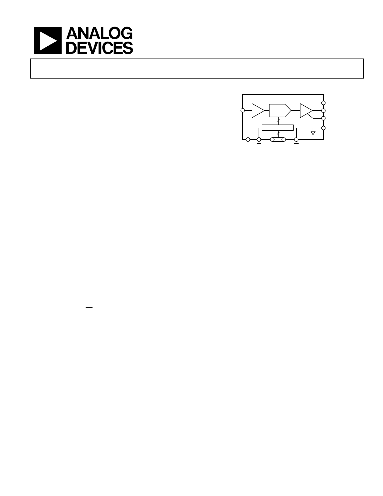
FUNCTIONAL BLOCK DIAGRAM
AD7392
V
REF
12-BIT
DAC
12
DAC REGISTER
12
Figure 1.
RSD0 TO D11CSDGND
Both parts are offered with similar pinouts, which allows users
to select the amount of resolution appropriate for their applications without changing the circuit card.
The AD7392/AD7393 are specified for operation over the
extended industrial temperature range of −40°C to +85°C.
The AD7393AR is specified for the automotive temperature
range of −40°C to +125°C. The AD7392/AD7393 are available
in 20-lead PDIP and 20-lead SOIC packages.
For serial data input, 8-lead packaged versions, see the AD7390
and AD7391.
V
DD
V
OUT
SHDN
AGND
1121 -0 01
Rev. C
Information furnished by Analog Devices is believed to be accurate and reliable. However, no
responsibility is assumed by Anal og Devices for its use, nor for any infringements of patents or ot her
rights of third parties that may result from its use. Specifications subject to change without notice. No
license is granted by implication or otherwise under any patent or patent rights of Analog Devices.
Trademarks and registered trademarks are the property of their respective owners.
One Technology Way, P.O. Box 9106, Norwood, MA 02062-9106, U.S.A.
Tel: 781.329.4700 www.analog.com
Fax: 781.461.3113 ©1996–2007 Analog Devices, Inc. All rights reserved.

AD7392/AD7393
TABLE OF CONTENTS
Features.............................................................................................. 1
Applications....................................................................................... 1
Functional Block Diagram .............................................................. 1
General Description ......................................................................... 1
Revision History ............................................................................... 2
Specifications..................................................................................... 3
Electrical Characteristics ............................................................. 3
Timing Diagram........................................................................... 5
Absolute Maximum Ratings............................................................ 6
ESD Caution.................................................................................. 6
Pin Configurations and Function Descriptions ........................... 7
Typical Performance Characteristics ............................................. 8
Theory of Operation ...................................................................... 12
REVISION HISTORY
8/07—Rev. B to Rev. C
Changes to Specifications Section.................................................. 3
Changes to Table 3............................................................................ 6
Changes to Theory of Operation Section.................................... 12
Changes to Figure 29...................................................................... 13
Changes to Figure 32...................................................................... 14
Changes to Figure 33...................................................................... 15
Updated Outline Dimensions....................................................... 16
Changes to Ordering Guide.......................................................... 17
6/04—Changed from Rev. A to Rev. B
Removed TSSOP.................................................................Universal
Changes to Ordering Guide.......................................................... 17
3/99—Changed from Rev. 0 to Rev. A
11/96—Revision 0: Initial Version
Digital-to-Analog Converters................................................... 12
Amplifier Section ....................................................................... 12
Reference Input........................................................................... 12
Power Supply............................................................................... 13
Input Logic Levels ...................................................................... 13
Digital Interface.......................................................................... 13
Reset Pin (
Power Shutdown (
Unipolar Output Operation...................................................... 14
Bipolar Output Operation......................................................... 15
Outline Dimensions....................................................................... 16
Ordering Guide .......................................................................... 17
RS
) ............................................................................. 14
SHDN
)......................................................... 14
Rev. C | Page 2 of 20

AD7392/AD7393
SPECIFICATIONS
ELECTRICAL CHARACTERISTICS
At V
= 2.5 V, −40°C < TA < +85°C, unless otherwise noted.
REF
Table 1. AD7392
Parameter Symbol Conditions 3 V ± 10% 5 V ± 10% Unit
STATIC PERFORMANCE
Resolution1 N 12 12 Bits
Relative Accuracy2 INL TA = +25°C ±1.8 ±1.8 LSB max
T
Differential Nonlinearity2 DNL TA = +25°C, monotonic ±0.9 ±0.9 LSB max
Monotonic ±1 ±1 LSB max
Zero-Scale Error V
Data = 0x000, TA = +25°C, +85°C 4.0 4.0 mV max
ZSE
Data = 0x000, TA = −40°C 8.0 8.0 mV max
Full-Scale Voltage Error V
TA = +25°C, +85°C, data = 0xFFF ±8 ±8 mV max
FSE
T
Full-Scale Temperature Coefficient3 TCVFS 28 28 ppm/°C typ
REFERENCE INPUT
V
Range V
REF
Input Resistance R
Input Capacitance3 C
0/VDD 0/VDD V min/max
REF
2.5 2.5 MΩ typ4
REF
5 5 pF typ
REF
ANALOG OUTPUT
Current (Source) I
Output Current (Sink) I
Data = 0x800, ∆ V
OUT
Data = 0x800, ∆ V
OUT
Capacitive Load3 CL No oscillation 100 100 pF typ
LOGIC INPUTS
Logic Input Low Voltage VIL 0.5 0.8 V max
Logic Input High Voltage VIH VDD − 0.6 VDD − 0.6 V min
Input Leakage Current IIL 10 10 μA max
Input Capacitance3 CIL 10 10 pF max
INTERFACE TIMING
3, 5
Chip Select Write Width tCS 45 45 ns min
Data Setup tDS 30 15 ns min
Data Hold tDH 20 5 ns min
Reset Pulse Width tRS 40 30 ns min
AC CHARACTERISTICS
Output Slew Rate SR Data = 0x000 to 0xFFF to 0x000 0.05 0.05 V/μs typ
Settling Time6 tS To ±0.1% of full scale 70 60 μs typ
Shutdown Recovery Time t
80 μs typ
SDR
DAC Glitch Code 0x7FF to Code 0x800 to Code 0x7FF 65 65 nV/s typ
Digital Feedthrough 15 15 nV/s typ
Feedthrough V
OUT/VREF
SUPPLY CHARACTERISTICS
Power Supply Range VDD
RANGE
Positive Supply Current IDD VIL = 0 V, no load 55/100 55/100 μA typ/max
Shutdown Supply Current I
Power Dissipation P
DD-SD
VIL = 0 V, no load 300 500 μW max
DISS
Power Supply Sensitivity PSS Δ VDD = ±5% 0.006 0.006 %/% max
1
One LSB = V
2
The first two codes (0x000, 0x001) are excluded from the linearity error measurement.
3
These parameters are guaranteed by design and not subject to production testing.
4
Typicals represent average readings measured at +25°C.
5
All input control signals are specified with tR = tF = 2 ns (10% to 90% of 13 V) and timed from a voltage level of 1.6 V.
6
The settling time specification does not apply for negative going transitions within the last 3 LSBs of ground.
/4096 V for the 12-bit AD7392.
REF
= −40°C, +85°C ±3 ±3 LSB max
A
= −40°C, data = 0xFFF ±20 ±20 mV max
A
= 5 LSB 1 1 mA typ
OUT
= 5 LSB 3 3 mA typ
OUT
V
= 1.5 V dc + 1 V p-p, data = 0x000,
REF
−63 −63 dB typ
f = 100 kHz
DNL < ±1 LSB 2.7/5.5 2.7/5.5 V min/max
SHDN
= 0, VIL = 0 V, no load
0.1/1.5 0.1/1.5 μA typ/max
Rev. C | Page 3 of 20

AD7392/AD7393
At V
= 2.5 V, −40°C < TA < +85°C, unless otherwise noted.
REF
Table 2. AD7393
Parameter Symbol Conditions 3 V ± 10% 5 V ± 10% Unit
STATIC PERFORMANCE
Resolution1 N 10 10 Bits
Relative Accuracy2 INL TA = +25°C ±1.75 ±1.75 LSB max
T
Differential Nonlinearity2 DNL Monotonic ±0.8 ±0.8 LSB max
Zero-Scale Error V
Full-Scale Voltage Error V
Data = 0x000 9.0 9.0 mV max
ZSE
TA = +25°C, +85°C, +125°C, data = 0x3FF ±32 ±32 mV max
FSE
T
Full-Scale Temperature Coefficient3 TCVFS 28 28 ppm/°C typ
REFERENCE INPUT
V
Range V
REF IN
Input Resistance R
Input Capacitance3 C
0/VDD 0/VDD V min/max
REF
2.5 2.5 MΩ typ4
REF
5 5 pF typ
REF
ANALOG OUTPUT
Output Current (Source) I
Output Current (Sink) I
Data = 0x200, Δ V
OUT
Data = 0x200, Δ V
OUT
Capacitive Load3 CL No oscillation 100 100 pF typ
LOGIC INPUTS
Logic Input Low Voltage VIL 0.5 0.8 V max
Logic Input High Voltage VIH VDD − 0.6 VDD − 0.6 V min
Input Leakage Current IIL 10 10 μA max
Input Capacitance3 CIL 10 10 pF max
INTERFACE TIMING
3, 5
Chip Select Write Width tCS 45 45 ns
Data Setup tDS 30 15 ns
Data Hold tDH 20 5 ns
Reset Pulse Width tRS 40 30 ns
AC CHARACTERISTICS
Output Slew Rate SR Data = 0x000 to 0x3FF to 0x000 0.05 0.05 V/μs typ
Settling Time6 tS To ±0.1% of full scale 70 60 μs typ
Shutdown Recovery Time t
80 μs typ
SDR
DAC Glitch Code 0x7FF to Code 0x800 to Code 0x7FF 65 65 nV/s typ
Digital Feedthrough 15 15 nV/s typ
Feedthrough V
OUT/VREF
SUPPLY CHARACTERISTICS
Power Supply Range VDD
RANGE
Positive Supply Current IDD VIL = 0 V, no load, TA = +25°C 55 55 μA typ
V
Shutdown Supply Current I
Power Dissipation P
DD-SD
VIL = 0 V, no load 300 500 μW max
DISS
Power Supply Sensitivity PSS Δ VDD = ±5% 0.006 0.006 %/% max
1
One LSB = V
2
The first two codes (0x000, 0x001) are excluded from the linearity error measurement.
3
These parameters are guaranteed by design and not subject to production testing.
4
Typicals represent average readings measured at +25°C.
5
All input control signals are specified with tR = tF = 2 ns (10% to 90% of 13 V) and timed from a voltage level of 1.6 V.
6
The settling time specification does not apply for negative going transitions within the last 3 LSBs of ground.
/1024 V for the 10-bit AD7393.
REF
= −40°C, +85°C, +125°C ±2.0 ±2.0 LSB max
A
= −40°C, data = 0x3FF ±42 ±42 mV max
A
= 5 LSB 1 1 mA typ
OUT
= 5 LSB 3 3 mA typ
OUT
V
= 1.5 V dc 11 V p-p, data = 0x000, f = 100 kHz −63 −63 dB typ
REF
DNL < ±1 LSB 2.7/5.5 2.7/5.5 V min/max
= 0 V, no load 100 100 μA max
IL
SHDN
= 0, VIL = 0 V, no load
0.1/1.5 0.1/1.5 μA typ/max
Rev. C | Page 4 of 20
AD7392/AD7393
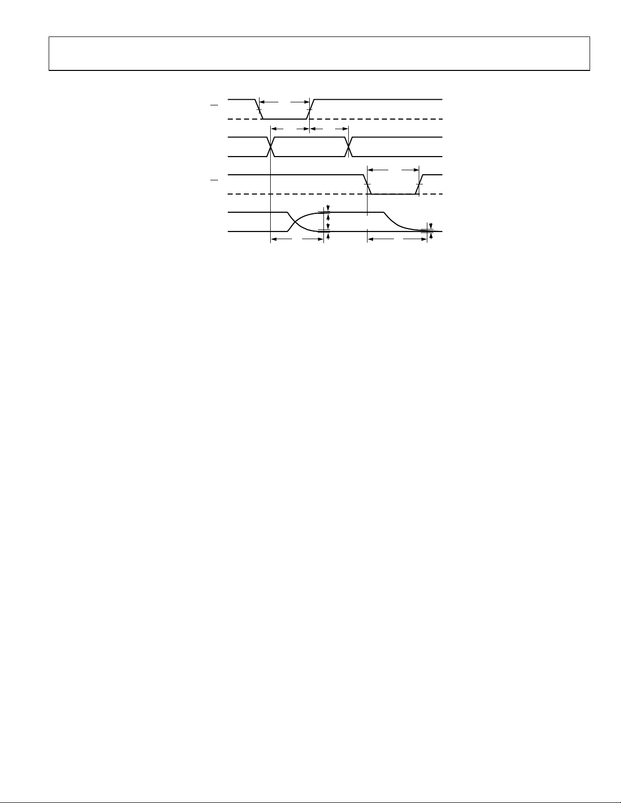
TIMING DIAGRAM
1
CS
0
1
D11 TO D0
0
1
RS
0
t
CS
t
DS
DATA VALID
t
DH
t
RS
FS
V
OUT
ZS
t
S
±0.1%FS
ERROR BAND
t
S
1121 -0 04
Figure 2. Timing Diagram
Rev. C | Page 5 of 20
AD7392/AD7393
ABSOLUTE MAXIMUM RATINGS
Table 3.
Parameter Rating
VDD to GND −0.3 V, +8 V
V
to GND −0.3 V, VDD
REF
Logic Inputs to GND −0.3 V, VDD + 0.3 V
V
to GND −0.3 V, VDD + 0.3 V
OUT
I
Short Circuit to GND 50 mA
OUT
DGND to AGND −0.3 V, +2 V
Package Power Dissipation (TJ max − TA)/θJA
Thermal Resistance (θJA)
20-Lead PDIP (N 20) 57°C/W
20-Lead SOIC (R-20) 60°C/W
Maximum Junction Temperature (TJ max) 150°C
Operating Temperature Range −40°C to +85°C
AD7393AR −40°C to +125°C
Storage Temperature Range −65°C to +150°C
Lead Temperature
Reflow Soldering Peak Temperature
SnPb 240°C
Pb-Free 260°C
Stresses above those listed under Absolute Maximum Ratings
may cause permanent damage to the device. This is a stress
rating only; functional operation of the device at these or any
other conditions above those indicated in the operational
section of this specification is not implied. Exposure to absolute
maximum rating conditions for extended periods may affect
device reliability.
ESD CAUTION
Rev. C | Page 6 of 20
 Loading...