

Low Cost, Low Power,
FULL
WAVE
RECTIFIER
INPUT
AMPLIFIER
RMS CORE
COM
+V
S
OUTPUT
C
AV
–V
S
POWER
DOWN
V
IN
C
C
8kV
AD737
BIAS
SECTION
8kV
8
7
6
5
1
2
3
4
a
True RMS-to-DC Converter
AD737*
FEATURES
COMPUTES
True RMS Value
Average Rectified Value
Absolute Value
PROVIDES
200 mV Full-Scale Input Range
(Larger Inputs with Input Attenuator)
Direct Interfacing with 3 1/2 Digit
CMOS A/D Converters
High Input Impedance of 10
12
⍀
Low Input Bias Current: 25 pA max
High Accuracy: ⴞ0.2 mV ⴞ0.3% of Reading
RMS Conversion with Signal Crest Factors Up to 5
Wide Power Supply Range: +2.8 V, –3.2 V to ⴞ16.5 V
Low Power: 160 A max Supply Current
No External Trims Needed for Specified Accuracy
AD736—A General Purpose, Buffered Voltage
Output Version Also Available
PRODUCT DESCRIPTION
The AD737 is a low power, precision, monolithic true rms-to-dc
converter. It is laser trimmed to provide a maximum error of
±0.2 mV ±0.3% of reading with sine-wave inputs. Furthermore,
it maintains high accuracy while measuring a wide range of
input waveforms, including variable duty cycle pulses and triac
(phase) controlled sine waves. The low cost and small physical
size of this converter make it suitable for upgrading the performance of non-rms “precision rectifiers” in many applications.
Compared to these circuits, the AD737 offers higher accuracy at
equal or lower cost.
The AD737 can compute the rms value of both ac and dc input
voltages. It can also be operated ac coupled by adding one external capacitor. In this mode, the AD737 can resolve input sig-
nal levels of 100 µV rms or less, despite variations in temperature
or supply voltage. High accuracy is also maintained for input
waveforms with crest factors of 1 to 3. In addition, crest factors
The AD737 allows the choice of two signal input terminals: a
high impedance (10
with high Z input attenuators and a low impedance (8 kΩ) input
which allows the measurement of 300 mV input levels, while
operating from the minimum power supply voltage of +2.8 V,
–3.2 V. The two inputs may be used either singly or differentially.
The AD737 achieves a 1% of reading error bandwidth exceeding 10 kHz for input amplitudes from 20 mV rms to 200 mV
rms while consuming only 0.72 mW.
The AD737 is available in four performance grades. The
AD737J and AD737K grades are rated over the commercial
temperature range of 0°C to +70°C. The AD737A and AD737B
grades are rated over the industrial temperature range of –40°C
to +85°C.
The AD737 is available in three low-cost, 8-lead packages: plastic DIP, plastic SO and hermetic cerdip.
as high as 5 can be measured (while introducing only 2.5%
additional error) at the 200 mV full-scale input level.
The AD737 has no output buffer amplifier, thereby significantly
reducing dc offset errors occuring at the output. This allows the
device to be highly compatible with high input impedance A/D
converters.
Requiring only 160 µA of power supply current, the AD737 is
optimized for use in portable multimeters and other battery
powered applications. This converter also provides a “power
PRODUCT HIGHLIGHTS
1. The AD737 is capable of computing the average rectified
value, absolute value or true rms value of various input
signals.
2. Only one external component, an averaging capacitor, is
required for the AD737 to perform true rms measurement.
3. The low power consumption of 0.72 mW makes the AD737
suitable for many battery powered applications.
down” feature which reduces the power supply standby current
to less than 30 µA.
*Protected under U.S. Patent Number 5,495,245.
REV. C
Information furnished by Analog Devices is believed to be accurate and
reliable. However, no responsibility is assumed by Analog Devices for its
use, nor for any infringements of patents or other rights of third parties
which may result from its use. No license is granted by implication or
otherwise under any patent or patent rights of Analog Devices.
One Technology Way, P.O. Box 9106, Norwood, MA 02062-9106, U.S.A.
Tel: 781/329-4700 World Wide Web Site: http://www.analog.com
Fax: 781/326-8703 © Analog Devices, Inc., 1999
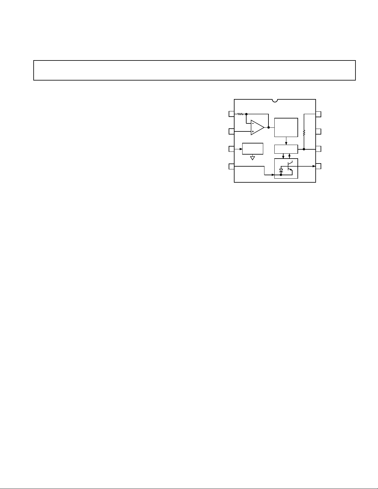
FUNCTIONAL BLOCK DIAGRAM
12
Ω) FET input which will directly interface

(@ +25ⴗC, ⴞ5 V supplies, ac coupled with 1 kHz sine-wave input applied unless
AD737–SPECIFICATIONS
Model Conditions Min Typ Max Min Typ Max Units
TRANSFER FUNCTION
CONVERSION ACCURACY 1 kHz Sine Wave
Total Error, Internal Trim
All Grades 0–200 mV rms 0.2/0.3 0.4/0.5 0.2/0.2 0.2/0.3 ±mV/±% of Reading
T
MIN-TMAX
A&B Grades @ 200 mV rms 0.5/0.7 0.3/0.5 ±mV/±% of Reading
J&K Grades @ 200 mV rms 0.007 0.007 ±% of Reading/°C
vs. Supply Voltage
@ 200 mV rms Input V
@ 200 mV rms Input V
dc Reversal Error, dc Coupled @ 600 mV dc 1.3 2.5 1.3 2.5 % of Reading
Nonlinearity
2
, 0–200 mV @ 100 mV rms 0 +0.25 +0.35 0 +0.25 +0.35 % of Reading
Total Error, External Trim 0–200 mV rms 0.1/0.2 0.1/0.2 ±mV/±% of Reading
ERROR vs. CREST FACTOR
Crest Factor 1 to 3 CAV, C
Crest Factor = 5 CAV, C
INPUT CHARACTERISTICS
High Impedance Input (Pin 2)
Signal Range
Continuous rms Level V
Continuous rms Level V
Peak Transient Input V
Peak Transient Input V
Peak Transient Input V
Input Resistance 10
Input Bias Current V
Low Impedance Input (Pin 1)
Signal Range
Continuous rms Level V
Continuous rms Level V
Peak Transient Input V
Peak Transient Input V
Peak Transient Input V
Input Resistance 6.4 8 9.6 6.4 8 9.6 kΩ
Maximum Continuous
Nondestructive Input All Supply Voltages ±12 ±12 V p-p
Input Offset Voltage
J&K Grades ⴞ3 ⴞ3 mV
A&B Grades ⴞ3 ⴞ3 mV
vs. Temperature 8 30 8 30 µV/°C
vs. Supply V
vs. Supply V
OUTPUT CHARACTERISTICS
Output Voltage Swing
No Load V
No Load V
No Load V
Output Resistance @ dc 6.4 8 9.6 6.4 8 9.6 kΩ
FREQUENCY RESPONSE
High Impedance Input (Pin 2)
For 1% Additional Error Sine-Wave Input
V
= 1 mV rms 1 1 kHz
IN
V
= 10 mV rms 6 6 kHz
IN
V
= 100 mV rms 37 37 kHz
IN
V
= 200 mV rms 33 33 kHz
IN
±3 dB Bandwidth Sine-Wave Input
= 1 mV rms 5 5 kHz
V
IN
V
= 10 mV rms 55 55 kHz
IN
V
= 100 mV rms 170 170 kHz
IN
VIN = 200 mV rms 190 190 kHz
1
ac Coupled Using C
200 mV–1 V rms –1.2 ⴞ2.0 –1.2 ⴞ2.0 % of Reading
= ±5 V to ±16.5 V 0 +0.06 +0.1 0 +0.06 +0.1 %/V
S
= ±5 V to ±3 V 0 –0.18 –0.3 0 –0.18 –0.3 %/V
S
3
= 100 µF 0.7 0.7 % Additional Error
F
= 100 µF 2.5 2.5 % Additional Error
F
= +2.8 V, –3.2 V 200 200 mV rms
S
= ±5 V to ±16.5 V 11V rms
S
= +2.8 V, –3.2 V ⴞ0.9 ⴞ0.9 V
S
= ±5 V ±2.7 ±2.7 V
S
= ±16.5 V ⴞ4.0 ⴞ4.0 V
S
= ±5 V 1 25 1 25 pA
S
= +2.8 V, –3.2 V 300 300 mV rms
S
= ±5 V to ±16.5 V l l V rms
S
= +2.8 V, –3.2 V ±1.7 ±1.7 V
S
= ±5 V ±3.8 ±3.8 V
S
= ±16.5 V ±11 ±11 V
S
4
ac Coupled
= ±5 V to ±16.5 V 50 150 50 150 µV/V
S
= ±5 V to ±3 V 80 80 µV/V
S
= +2.8 V, –3.2 V 0 to –1.6 –1.7 0 to –1.6 –1.7 V
S
= ±5 V 0 to –3.3 –3.4 0 to –3.3 –3.4 V
S
= ±16.5 V 0 to –4 –5 0 to –4 –5 V
S
otherwise noted.)
AD737J/A AD737K/B
V
= Avg.(V
OUT
C
2
)
IN
12
V
OUT
= Avg.(V
10
2
)
IN
12
Ω
REV. C–2–
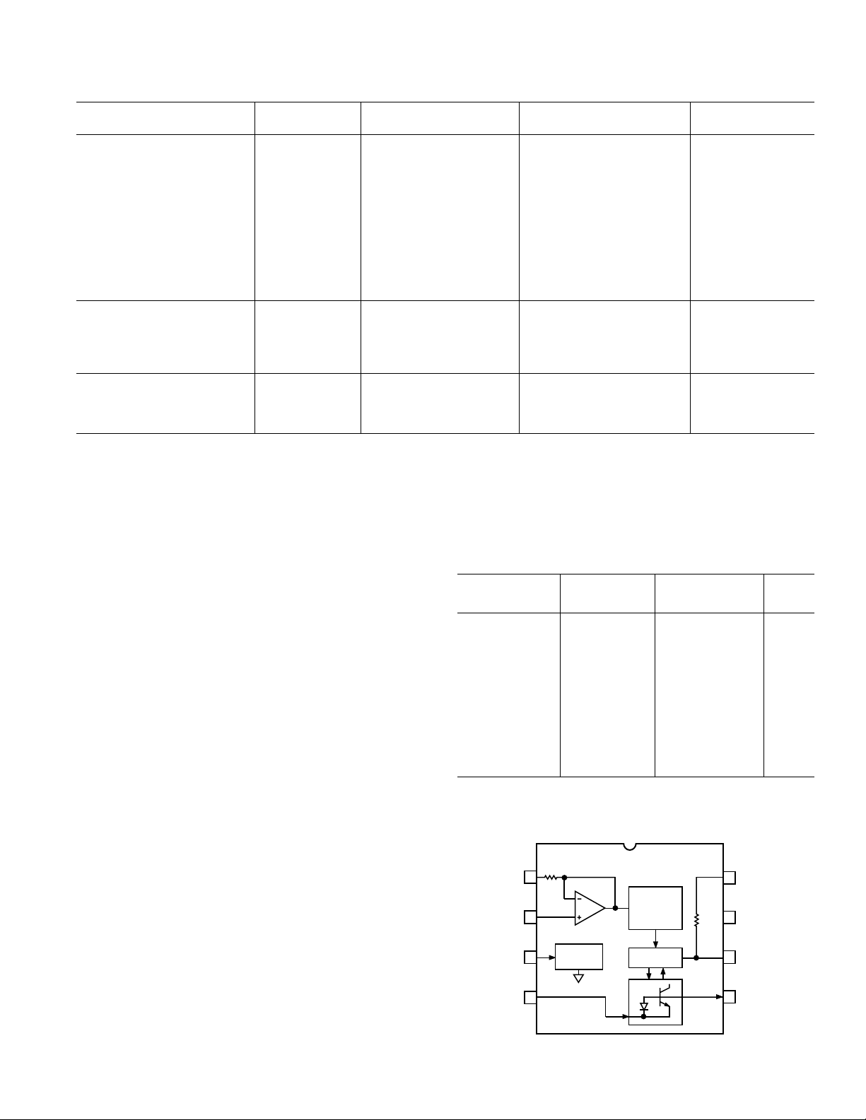
AD737J/A AD737K/B
FULL
WAVE
RECTIFIER
INPUT
AMPLIFIER
RMS CORE
COM
+V
S
OUTPUT
C
AV
–V
S
POWER
DOWN
V
IN
C
C
8kV
AD737
BIAS
SECTION
8kV
8
7
6
5
1
2
3
4
Model Conditions Min Typ Max Min Typ Max Units
FREQUENCY RESPONSE
Low Impedance Input (Pin 1)
For 1% Additional Error Sine-Wave Input
V
= 1 mV rms 1 1 kHz
IN
V
= 10 mV rms 6 6 kHz
IN
V
= 100 mV rms 90 90 kHz
IN
V
= 200 mV rms 90 90 kHz
IN
±3 dB Bandwidth Sine-Wave Input
= 1 mV rms 5 5 kHz
V
IN
V
= 10 mV rms 55 55 kHz
IN
V
= 100 mV rms 350 350 kHz
IN
VIN = 200 mV rms 460 460 kHz
POWER SUPPLY
Operating Voltage Range +2.8, –3.2 ±5 ±16.5 +2.8, –3.2 ±5 ±16.5 V
Quiescent Current Zero Signal 120 160 120 160 µA
V
= 200 mV rms, No Load Sine-Wave Input 170 210 170 210 µA
IN
Power Down Mode Current Pin 3 Tied to +V
S
25 40 25 40 µA
TEMPERATURE RANGE
Operating, Rated Performance
Commercial (0°C to +70°C) AD737J AD737K
Industrial (–40°C to +85°C) AD737A AD737B
NOTES
l
Accuracy is specified with the AD737 connected as shown in Figure 16 with capacitor CC.
2
Nonlinearity is defined as the maximum deviation (in percent error) from a straight line connecting the readings at 0 and 200 mV rms.
3
Error vs. Crest Factor is specified as additional error for a 200 mV rms signal. C.F. = V
4
DC offset does not limit ac resolution.
Specifications are subject to change without notice.
Specifications shown in boldface are tested on all production units at final electrical test. Results from those tests are used to calculate outgoing quality levels.
PEAK
/V rms.
AD737
ABSOLUTE MAXIMUM RATINGS
Supply Voltage . . . . . . . . . . . . . . . . . . . . . . . . . . . . . . . ±16.5 V
Internal Power Dissipation
2
. . . . . . . . . . . . . . . . . . . . . 200 mW
1
Input Voltage . . . . . . . . . . . . . . . . . . . . . . . . . . . . . . . . . . . . . .
Output Short-Circuit Duration . . . . . . . . . . . . . . . . . Indefinite
Differential Input Voltage . . . . . . . . . . . . . . . . . . +V
and –V
S
S
Storage Temperature Range (Q) . . . . . . –65°C to +150°C
Storage Temperature Range (N, R) . . . . . –65°C to +125°C
Operating Temperature Range
AD737J/K . . . . . . . . . . . . . . . . . . . . . . . . . . . 0°C to +70°C
AD737A/B . . . . . . . . . . . . . . . . . . . . . . . . . .–40°C to +85°C
Lead Temperature Range (Soldering 60 sec) . . . . . . . . +300°C
ESD Rating . . . . . . . . . . . . . . . . . . . . . . . . . . . . . . . . . . .500 V
NOTES
1
Stresses above those listed under Absolute Maximum Ratings may cause perma-
Model Range Description Option
AD737AQ –40°C to +85°C Cerdip Q-8
AD737BQ –40°C to +85°C Cerdip Q-8
AD737JN 0°C to +70°C Plastic DIP N-8
AD737JR 0°C to +70°C SOIC SO-8
AD737JR-REEL 0°C to +70°C 13" Tape and Reel SO-8
AD737JR-REEL7 0°C to +70°C 7" Tape and Reel SO-8
AD737KN 0°C to +70°C Plastic DIP N-8
AD737KR 0°C to +70°C SOIC SO-8
AD737KR-REEL 0°C to +70°C 13" Tape and Reel SO-8
AD737KR-REEL7 0°C to +70°C 7" Tape and Reel SO-8
ORDERING GUIDE
Temperature Package Package
nent damage to the device. This is a stress rating only; functional operation of the
device at these or any other conditions above those indicated in the operational
section of this specification is not implied. Exposure to absolute maximum rating
conditions for extended periods may affect device reliability.
2
8-Lead Plastic DIP Package: θJA = 165°C/W
8-Lead Cerdip Package: θ
= 110°C/W
JA
Plastic DIP (N-8), Cerdip (Q-8), SOIC (SO-8)
PIN CONFIGURATIONS
8-Lead Small Outline Package: θJA = 155°C/W
REV. C –3–

AD737
–Typical Characteristics
Figure 1. Additional Error vs.
Supply Voltage
Figure 4. Frequency Response
Driving Pin 1
Figure 2. Maximum Input Level
vs. Supply Voltage
Figure 5. Frequency Response
Driving Pin 2
Figure 3. Power Down Current vs.
Supply Voltage
Figure 6. Additional Error vs.
Crest Factor vs. C
AV
Figure 7. Additional Error vs.
Temperature
Figure 8. DC Supply Current vs.
RMS lnput Level
Figure 9. 23 dB Frequency vs.
RMS Input Level (Pin 2)
REV. C–4–

Applying the
AD737
Figure 10. Error vs. RMS Input
Voltage (Pin 2) Using Circuit
of Figure 21
Figure 13. Pin 2 Input Bias
Current vs. Supply Voltage
CALCULATING SETTLING TIME USING FIGURE 14
The graph of Figure 14 may be used to closely approximate the
time required for the AD737 to settle when its input level is re-
duced in amplitude. The net time required for the rms converter
to settle will be the difference between two times extracted from
the graph – the initial time minus the final settling time. As an
example, consider the following conditions: a 33 µF averaging
capacitor, an initial rms input level of 100 mV and a final (re-
duced) input level of 1 mV. From Figure 14, the initial settling
time (where the 100 mV line intersects the 33 µF line) is around
80 ms. The settling time corresponding to the new or final input
level of 1 mV is approximately 8 seconds. Therefore, the net
time for the circuit to settle to its new value will be 8 seconds
minus 80 ms which is 7.92 seconds. Note that, because of the
smooth decay characteristic inherent with a capacitor/diode
combination, this is the total settling time to the final value (i.e.,
not the settling time to 1%, 0.1%, etc., of final value). Also, this
graph provides the worst case settling time, since the AD737
will settle very quickly with increasing input levels.
Figure 11. CAV vs. Frequency for
Specified Averaging Error
Figure 14. Settling Time vs. RMS
Input Level for Various Values of C
Figure 12. RMS Input Level vs.
Frequency for Specified Averaging
Error
Figure 15. Pin 2 Input Bias Current
vs. Temperature
AV
TYPES OF AC MEASUREMENT
The AD737 is capable of measuring ac signals by operating as
either an average responding or a true rms-to-de converter. As
its name implies, an average responding converter computes the
average absolute value of an ac (or ac and dc) voltage or current
by full wave rectifying and low-pass filtering the input signal;
this will approximate the average. The resulting output, a dc
“average” level, is then scaled by adding (or reducing) gain; this
scale factor converts the dc average reading to an rms equivalent
value for the waveform being measured. For example, the average absolute value of a sine-wave voltage is 0.636 that of V
the corresponding rms value is 0.707 times V
for sine-wave voltages, the required scale factor is 1.11 (0.707
divided by 0.636).
In contrast to measuring the “average” value, true rms measurement is a “universal language” among waveforms, allowing the
magnitudes of all types of voltage (or current) waveforms to be
compared to one another and to dc. RMS is a direct measure of
the power or heating value of an ac voltage compared to that of
dc: an ac signal of 1 volt rms will produce the same amount of
heat in a resistor as a 1 volt dc signal.
. Therefore,
PEAK
PEAK
;
REV. C –5–

AD737
Table I. Error Introduced by an Average Responding Circuit When Measuring Common Waveforms
Waveform Type Crest Factor True rms Value Average Responding % of Reading Error*
1 Volt Peak (V
/V rms) Circuit Calibrated to Using Average
PEAK
Amplitude Read rms Value of Responding Circuit
Sine Waves Will Read
Undistorted 1.414 0.707 V 0.707 V 0%
Sine Wave
Symmetrical
Square Wave 1.00 1.00 V 1.11 V +11.0%
Undistorted
Triangle Wave 1.73 0.577 V 0.555 V –3.8%
Gaussian
Noise (98% of
Peaks <1 V) 3 0.333 V 0.295 V –11.4%
Rectangular 2 0.5 V 0.278 V –44%
Pulse Train 10 0.1 V 0.011 V –89%
SCR Waveforms
50% Duty Cycle 2 0.495 V 0.354 V –28%
25% Duty Cycle 4.7 0.212 V 0.150 V –30%
Mathematically, the rms value of a voltage is defined (using a
simplified equation) as:
V rms = Avg .(V
2
)
This involves squaring the signal, taking the average, and then
obtaining the square root. True rms converters are “smart rectifiers”: they provide an accurate rms reading regardless of the
type of waveform being measured. However, average responding
converters can exhibit very high errors when their input signals
deviate from their precalibrated waveform; the magnitude of the
error will depend upon the type of waveform being measured.
As an example, if an average responding converter is calibrated
to measure the rms value of sine-wave voltages, and then is used
to measure either symmetrical square waves or de voltages, the
converter will have a computational error 11% (of reading)
higher than the true rms value (see Table I).
AD737 THEORY OF OPERATION
As shown by Figure 16, the AD737 has four functional subsections: input amplifier, full-wave rectifier, rms core and bias sections. The FET input amplifier allows both a high impedance,
buffered input (Pin 2) or a low impedance, wide-dynamic-range
C
C
10mF
(OPTIONAL
1
C
C
2
V
IN
POWER
3
DOWN
4
–V
S
POSITIVE SUPPLY
NEGATIVE SUPPLY
8kV
INPUT
AMPLIFIER
BIAS
SECTION
COMMON
AD737
FULL
WAVE
RECTIFIER
RMS
CORE
C
AV
33mF
0.1mF
0.1mF
8kV
COM
8
7
+V
OUTPUT
6
5
C
F
10mF
S
(OPTIONAL)
V
OUT
C
AV
+V
S
–V
S
Figure 16. AD737 True RMS Circuit
input (Pin 1). The high impedance input, with its low input
bias current, is well suited for use with high impedance input
attenuators. The input signal may be either dc or ac coupled
to the input amplifier. Unlike other rms converters, the AD737
permits both direct and indirect ac coupling of the inputs. AC
coupling is provided by placing a series capacitor between the
input signal and Pin 2 (or Pin 1) for direct coupling and
between Pin 1 and ground (while driving Pin 2) for indirect
coupling.
The output of the input amplifier drives a full-wave precision
rectifier, which in turn, drives the rms core. It is in the core that
the essential rms operations of squaring, averaging and square
rooting are performed, using an external averaging capacitor,
. Without CAV, the rectified input signal travels through the
C
AV
core unprocessed, as is done with the average responding connection (Figure 17).
A final subsection, the bias section, permits a “power down”
function. This reduces the idle current of the AD737 from 160
µA down to a mere 30 µA. This feature is selected by tying Pin
3 to the +V
terminal. In the average responding connection, all
S
of the averaging is carried out by an RC post filter consisting of
an 8 kΩ internal scale-factor resistor connected between Pins 6
and 8 and an external averaging capacitor, C
. In the rms cir-
F
cuit, this additional filtering stage helps reduce any output
ripple which was not removed by the averaging capacitor, C
AV
.
RMS MEASUREMENT – CHOOSING THE OPTIMUM
VALUE FOR C
AV
Since the external averaging capacitor, CAV, “holds” the rectified input signal during rms computation, its value directly affects the accuracy of the rms measurement, especially at low
frequencies. Furthermore, because the averaging capacitor appears across a diode in the rms core, the averaging time constant will increase exponentially as the input signal is reduced.
This means that as the input level decreases, errors due to
nonideal averaging will reduce while the time it takes for the circuit to settle to the new rms level will increase. Therefore, lower
input levels allow the circuit to perform better (due to increased
averaging) but increase the waiting time between measurements. Obviously, when selecting C
, a trade-off between
AV
computational accuracy and settling time is required.
REV. C–6–

AD737
RAPID SETTLING TIMES VIA THE AVERAGE
RESPONDING CONNECTION (FIGURE 17)
Because the average responding connection does not use an av-
eraging capacitor, its settling time does not vary with input sig-
nal level; it is determined solely by the RC time constant of C
F
and the internal 8 kΩ output scaling resistor.
Figure 17. AD737 Average Responding Circuit
DC ERROR, OUTPUT RIPPLE, AND AVERAGING
ERROR
Figure 18 shows the typical output waveform of the AD737 with
a sine-wave input voltage applied. As with all real-world devices,
the ideal output of V
= VIN is never exactly achieved; in-
OUT
stead, the output contains both a dc and an ac error component.
AC MEASUREMENT ACCURACY AND CREST FACTOR
The crest factor of the input waveform is often overlooked when
determining the accuracy of an ac measurement. Crest factor is
defined as the ratio of the peak signal amplitude to the rms amplitude (C.F. = V
/V rms). Many common waveforms, such
PEAK
as sine and triangle waves, have relatively low crest factors (≥2).
Other waveforms, such as low duty cycle pulse trains and SCR
waveforms, have high crest factors. These types of waveforms
require a long averaging time constant (to average out the long
time periods between pulses). Figure 6 shows the additional error vs. crest factor of the AD737 for various values of C
AV
.
SELECTING PRACTICAL VALUES FOR INPUT
COUPLING (C
(C
) CAPACITORS
F
), AVERAGING (CAV) AND FILTERING
C
Table II provides practical values of CAV and CF for several
common applications.
Table II. AD737 Capacitor Selection Chart
Application rms Low Max C
Input Frequency Crest Time*
Level Cutoff Factor to 1%
(–3 dB)
General Purpose 0–1 V 20 Hz 5 150 µF 10 µF 360 ms
rms Computation 200 Hz 5 15 µF1 µF 36 ms
0–200 mV 20 Hz 5 33 µF 10 µF 360 ms
200 Hz 5 3.3 µF1 µF 36 ms
General Purpose 0–1 V 20 Hz None 33 µF 1.2 sec
Average 200 Hz None 3.3 µF 120 ms
Responding
0–200 mV 20 Hz None 33 µF 1.2 sec
200 Hz None 3.3 µF 120 ms
SCR Waveform 0–200 mV 50 Hz 5 100 µF 33 µF 1.2 sec
Measurement 60 Hz 5 82 µF 27 µF 1.0 sec
CFSettling
AV
Figure 18. Output Waveform for Sine-Wave Input Voltage
As shown, the dc error is the difference between the average of
the output signal (when all the ripple in the output has been
removed by external filtering) and the ideal dc output. The dc
error component is therefore set solely by the value of averag-
ing capacitor used–no amount of post filtering (i.e., using a
very large C
) will allow the output voltage to equal its ideal
F
value. The ac error component, an output ripple, may be easily
removed by using a large enough post filtering capacitor, C
.
F
In most cases, the combined magnitudes of both the dc and ac error
components need to be considered when selecting appropriate values
for capacitors C
and CF. This combined error, representing the
AV
maximum uncertainty of the measurement is termed the “averaging
error” and is equal to the peak value of the output ripple plus the dc
error. As the input frequency increases, both error components de-
crease rapidly: if the input frequency doubles, the dc error and ripple
reduce to 1/4 and 1/2 their original values, respectively, and rapidly
become insignificant.
0–100 mV 50 Hz 5 50 µF 33 µF 1.2 sec
Audio
Applications
Speech 0–200 mV 300 Hz 3 1.5 µF 0.5 µF 18 ms
Music 0–100 mV 20 Hz 10 100 µF 68 µF 2.4 sec
* Settling time is specified over the stated rms input level with the input signal increasing
from zero. Settling times will be greater for decreasing amplitude input signals.
The input coupling capacitor, C
60 Hz 5 47 µF 27 µF 1.0 sec
, in conjunction with the 8 kΩ
C
internal input scaling resistor, determine the –3 dB low frequency rolloff. This frequency, F
F
=
L
2π(8, 000 )(TheValue of C
, is equal to:
L
1
C
in Farads )
Note that at FL, the amplitude error will be approximately –30%
(–3 dB) of reading. To reduce this error to 0.5% of reading,
choose a value of C
that sets FL at one tenth the lowest fre-
C
quency to be measured.
In addition, if the input voltage has more than 100 mV of dc
offset, than the ac coupling network at Pin 2 should be used in
addition to capacitor C
.
C
REV. C –7–

AD737
–Applications Circuits
Figure 19. 3 1/2 Digit DVM Circuit
Figure 20. Battery Powered Operation for 200 mV max
RMS Full-Scale Input
C1175b–0–12/99 (rev. C)
Figure 21. External Scale Factor Trim
0.1574 (4.00)
0.1497 (3.80)
PIN 1
0.0098 (0.25)
0.0040 (0.10)
SEATING
Figure 22. dB Output Connection
8-Lead Small Outline Package (SO-8)
0.1 968 (5.00)
0.1 890 (4.80)
85
0.0500 (1.27)
PLANE
0.2440 (6.20)
0.2284 (5.80)
41
BSC
0.0192 (0.49)
0.0138 (0.35)
0.0688 (1.75)
0.0532 (1.35)
0.0098 (0.25)
0.0075 (0.19)
0.0196 (0.50)
0.0099 (0.25)
88
0.0500 (1.27)
08
0.0160 (0.41)
Figure 23. DC Coupled VOS and Scale Factor Trims
OUTLINE DIMENSIONS
Dimensions shown in inches and (mm).
8-Lead Plastic DIP Package (N-8)
3 458
8-Lead Cerdip Package (Q-8)
PRINTED IN U.S.A.
REV. C–8–
 Loading...