Analog Devices AD7111 Datasheet

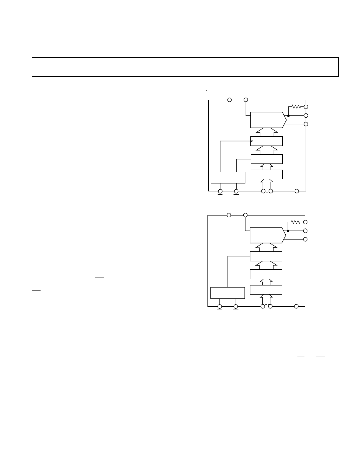
LC2MOS LOGDAC
17-BIT DAC
17-BIT LATCH
DECODE LOGIC
8-BIT BUFFER
CONTROL LOGIC
AD7111A
I
OUT
AGND
R
FB
V
DD
V
IN
DGND
CS
WR
D0 – D7
a
FEATURES
Dynamic Range: 88.5 dB
Resolution: 0.375 dB
On-Chip Data Latches
+5 V Operation
AD7111A Pin Compatible with AD7524
Low Power
APPLICATIONS
Audio Attenuators
Sonar Systems
Function Generators
Digitally Controlled AGC System
GENERAL DESCRIPTION
The LOGDAC AD7111/AD7111A are monolithic multiplying
D/A converters featuring wide dynamic range in a small package. Both DACs can attenuate an analog input signal over the
range 0 dB to 88.5 dB in 0.375 dB steps. They are available in
16-pin DIPs and SOIC packages. The AD7111 is also available
in a 20-terminal LCCC package.
The degree of attenuation across the DAC is determined by an
8-bit word applied to the onboard decode logic. This 8-bit word
is decoded into a 17-bit word which is then applied to a 17-bit
R-2R ladder. The very fine step resolution, which is available
over the entire dynamic range, is due to the use of this 17-bit
DAC.
The AD7111/AD7111A are easily interfaced to a standard 8-bit
MPU bus via an 8-bit data port and standard microprocessor
control lines. The AD7111
quires a rising edge to load new data to the DAC. The AD7111A
WR is level triggered to allow transparent operation of the
latches, if required. It should also be noted that the AD7111A is
exactly pin and function-compatible with the AD7524, an industry standard 8-bit multiplying DAC. This allows an easy upgrading of existing AD7524 designs which would benefit both
from the wider dynamic range and the finer step resolution offered by the AD7111A.
The AD7111/AD7111A are fabricated in Linear Compatible
CMOS (LC2MOS), an advanced, mixed technology process that
combines precision bipolar circuits with low power CMOS logic.
LOGDAC is a registered trademark of Analog Devices, Inc.
WR input is edge triggered and re-
Logarithmic D/A Converter
AD7111/AD7111A
FUNCTIONAL BLOCK DIAGRAMS
V
V
DD
IN
R
FB
AD7111
17-BIT DAC
17-BIT LATCH
DECODE LOGIC
CONTROL LOGIC
WR
CS
8-BIT BUFFER
D0 – D7
DGND
PRODUCT HIGHLIGHTS
1. Wide Dynamic Range: 0 dB to 88.5 dB attenuation range in
0.375 dB steps.
2. Small Package: The AD7111/AD7111A are available in
16-pin DIPs and SOIC packages.
3. Transparent Latch Operation: By tying the
puts low, the DAC latches in the AD7111A can be made
transparent.
4. Fast Microprocessor Interface: Data setup times of 25 ns and
write pulse width of 57 ns make the AD7111A compatible
with modern microprocessors.
I
OUT
AGND
CS and WR in-
REV. 0
Information furnished by Analog Devices is believed to be accurate and
reliable. However, no responsibility is assumed by Analog Devices for its
use, nor for any infringements of patents or other rights of third parties
which may result from its use. No license is granted by implication or
otherwise under any patent or patent rights of Analog Devices.
One Technology Way, P.O. Box 9106, Norwood, MA 02062-9106, U.S.A.
Tel: 617/329-4700 Fax: 617/326-8703

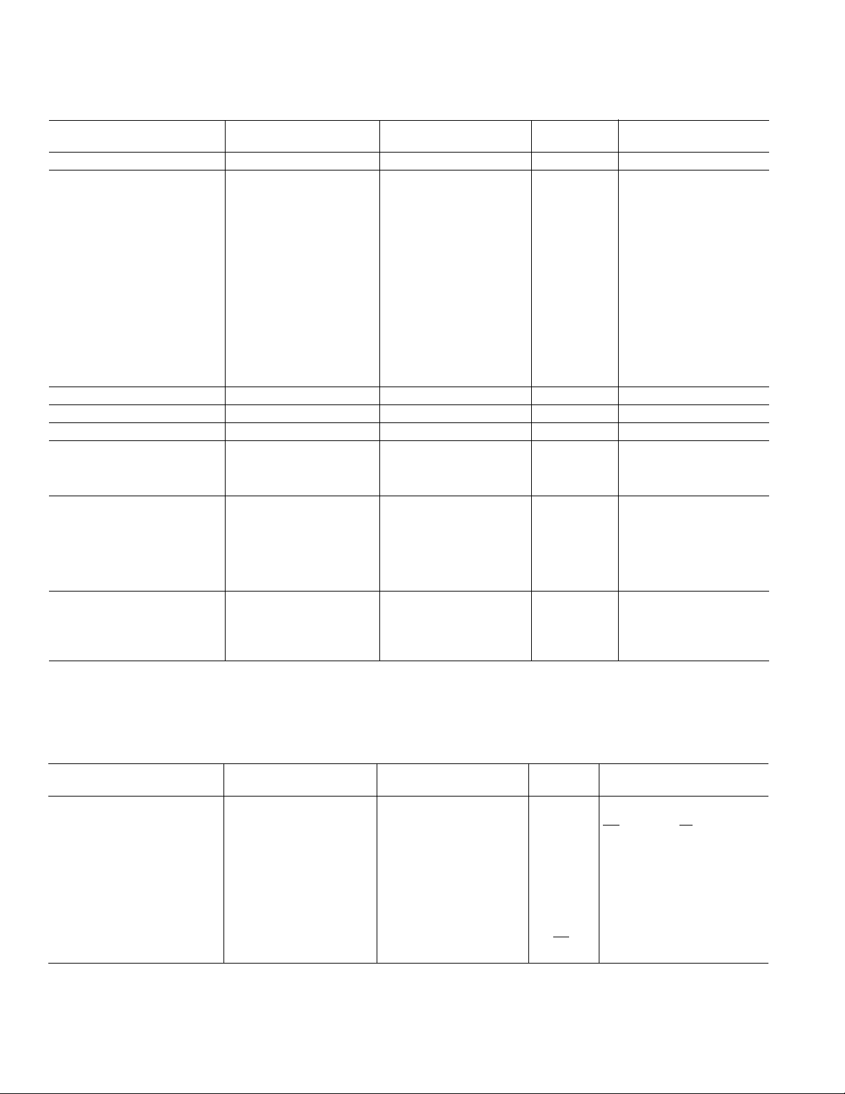
AD7111/AD7111A–SPECIFICA TIONS
(VDD = +5 V, VIN = –10 V dc, I
AD7111–ELECTRICAL CHARACTERISTICS
AD711 except where noted)
= AGND = DGND = O V output amplifier
OUT
Parameter TA = +258CTA = T
NOMINAL RESOLUTION 0.375 0.375 0.375 0.375 dB
ACCURACY RELATIVE TO
0 dB ATTENUATION
0.375 dB Steps:
Accuracy ≤ ±0.17 dB 0 to 36 0 to 36 0 to 30 0 to 30 dB min Guaranteed Attenuation Ranges
Monotonic 0 to 54 0 to 54 0 to 48 0 to 48 dB min for Specified Step Sizes
0.75 dB Steps:
Accuracy ≤ ±0.35 dB 0 to 48 0 to 42 0 to 42 0 to 36 dB min
Monotonic 0 to 72 0 to 66 0 to 72 0 to 60 dB min
1.5 dB Steps:
Accuracy ≤ ±0.7 dB 0 to 54 0 to 48 0 to 42 0 to 42 dB min Full Range Is from 0 dB
Monotonic Full Range 0 to 78 0 to 85.5 0 to 72 dB min to 88.5 dB
3.0 dB Steps:
Accuracy ≤ ±1.4 dB 0 to 66 0 to 54 0 to 60 0 to 48 dB min
Monotonic Full Range Full Range Full Range Full Range dB min
6.0 dB Steps:
Accuracy ≤ ±2.7 dB 0 to 72 0 to 60 0 to 60 0 to 48 dB min
Monotonic Full Range Full Range Full Range Full Range dB min
GAIN ERROR ± 0.1 ± 0.15 ± 0.15 ±0.20 dB max
VIN INPUT RESISTANCE 9/11/15 9/11/15 7/11/18 7/11/18 kΩ min/typ/max
RFB INPUT RESISTANCE 9.3/11.5/15.7 9.3/11.5/15.7 7.3/11.5/18.8 7.3/11.5/18.8 kΩ min/typ/max
DIGITAL INPUTS
VIH (Input High Voltage) 2.4 2.4 2.4 2.4 V min
VIL (Input Low Voltage) 0.8 0.8 0.8 0.8 V max
Input Leakage Current ± 1 ±10 ± 1 ± 10 µA max Digital Inputs = V
SWITCHING CHARACTERISTICS
t
CS
t
CH
t
WR
t
DS
t
DH
t
RFSH
POWER SUPPLY
V
DD
I
DD
NOTE
1
Sample tested at +25°C to ensure compliance.
Specifications subject to change without notice.
AD7111L/C/U Grades AD7111K/B/T Grades
1
0 0 0 0 ns min
0 0 0 0 ns min Chip Select to Write Hold Time
350 500 350 500 ns min Write Pulse Width
175 250 175 250 ns min Data Valid to Write Setup Time
10 10 10 10 ns min Data Valid to Write Hold Time
3 4.5 3 4.5 µs min Refresh Time
+5 +5 +5 +5 V
1 4 1 4 mA max Digital Inputs = VIL or V
500 1000 500 1000 µA max Digital Inputs = 0 V or VDD;
MIN
, T
MAXTA
= +258CTA = T
MIN
, T
Units Conditions/Comments
MAX
Chip Select to Write Setup Time
See Figure 6
DD
IH
AC PERFORMANCE CHARACTERISTICS
to test. VDD = +5 V, VIN = –10 V dc except where noted, I
Parameter TA = +258CTA = T
DC Supply Rejection, ∆Gain/∆V
Propagation Delay 3.0 4.5 3.0 4.5 µs max Full-Scale Change Measured from
Digital-to-Analog Glitch Impulse 100 100 nV secs typ Measured with AD843 as Output
Output Capacitance, Pin 1 185 185 185 185 pF max
Input Capacitance, Pin 15 and Pin 16 7 7 7 7 pF max
Feedthrough at 1 kHz –94 –72 –94 –68 dB max
Total Harmonic Distortion –91 –91 –91 –91 dB typ VIN = 6 V rms at 1 kHz
Output Noise Voltage Density 70 70 70 70 nV/√Hz max Includes AD711 Amplifier Noise
Digital Input Capacitance 7 7 7 7 pF max
Specifications subject to change without notice.
DD
AD7111L/C/U Grades AD7111K/B/T Grades
0.001 0.005 0.001 0.005 dB per % max
These characteristics are included for design guidance only and are not subject
= AGND = DGND = O V, output amplifier AD711 except where noted.
OUT
MIN
, T
MAXTA
= +258CTA = T
MIN
, T
Units Conditions/Comments
MAX
∆VDD = ±10%, Input Code = 00000000
WR Going High, CS = 0 V
Amplifier for Code Transition
10000000 to 00000000
C1 of Figure 1 is 0 pF
–2–
REV. 0

AD7111/AD7111A
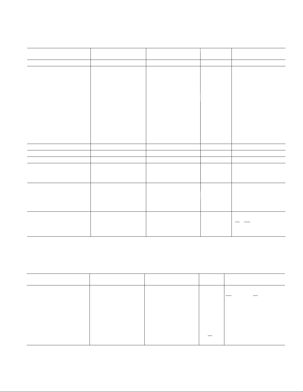
AD7111A–ELECTRICAL CHARACTERISTICS
(VDD = +5 V, VIN = –10 V dc, I
AD711 except where noted)
= AGND = DGND = O V output amplifier
OUT
AD7111AC Grade AD7111AB Grade
Parameter TA = +258CTA = T
MIN
, T
MAXTA
= +258CTA = T
MIN
, T
Units Conditions/Comments
MAX
NOMINAL RESOLUTION 0.375 0.375 0.375 0.375 dB
ACCURACY RELATIVE TO
0 dB ATTENUATION
0.375 dB Steps:
Accuracy ≤ ±0.17 dB 0 to 36 0 to 36 0 to 30 0 to 30 dB min Guaranteed Attenuation Ranges
Monotonic 0 to 54 0 to 54 0 to 48 0 to 48 dB min for Specified Step Sizes
0.75 dB Steps:
Accuracy ≤ ±0.35 dB 0 to 48 0 to 42 0 to 42 0 to 36 dB min
Monotonic 0 to 72 0 to 66 0 to 72 0 to 60 dB min
1.5 dB Steps:
Accuracy ≤ ±0.7 dB 0 to 54 0 to 48 0 to 48 0 to 42 dB min Full Range Is from 0 dB
Monotonic Full Range 0 to 78 0 to 85.5 0 to 72 dB min to 88.5 dB
3.0 dB Steps:
Accuracy ≤ ±1.4 dB 0 to 66 0 to 54 0 to 60 0 to 48 dB min
Monotonic Full Range Full Range Full Range Full Range dB min
6.0 dB Steps:
Accuracy ≤ ±2.7 dB 0 to 72 0 to 60 0 to 60 0 to 48 dB min
Monotonic Full Range Full Range Full Range Full Range dB min
GAIN ERROR ±0.1 ±0.15 ±0.15 ±0.20 dB max
VIN INPUT RESISTANCE 9/11/15 9/11/15 7/11/18 7/11/18 kΩ min/typ/max
RFB INPUT RESISTANCE 9.3/11.5/15.7 9.3/11.5/15.7 7.3/11.5/18.8 7.3/11.5/18.8 kΩ min/typ/max
DIGITAL INPUTS
VIH (Input High Voltage) 2.4 2.4 2.4 2.4 V min
VIL (Input High Voltage) 0.8 0.8 0.8 0.8 V max
Input Leakage Current ±1 ±10 ±1 ±10 µA max Digital Inputs = V
SWITCHING CHARACTERISTICS
t
CS
t
CH
t
WR
t
DS
t
DH
1
0 0 0 0 ns min
Chip Select to Write Setup Time
0 0 0 0 ns min Chip Select to Write Hold Time
57 57 57 57 ns min Write Pulse Width
25 25 25 25 ns min Data Valid to Write Setup Time
10 10 10 10 ns min Data Valid to Write Hold Time
POWER SUPPLY
V
DD
I
DD
+5 +5 +5 +5 V Digital Inputs = VIL or V
1 2 1 2 mA max CS = WR = 0 V
1 1 1 1 mA max Digital Inputs = 0 V or VDD;
See Figure 6
NOTE
1
Sample tested at +25°C to ensure compliance.
Specifications subject to change without notice.
DD
IH
AC PERFORMANCE CHARACTERISTICS
to test. VDD = +5 V, VIN = –10 V dc except where noted, I
These characteristics are included for design guidance only and are not subject
= AGND = DGND = O V, output amplifier AD711 except where noted.
OUT
AD7111AC Grade AD7111AB Grade
Parameter TA = +258CTA = T
DC Supply Rejection, ∆Gain/∆V
Propagation Delay 1 1.5 1 1.5 µs max Full-Scale Change Measured from
DD
0.001 0.005 0.001 0.005 dB per % max
MIN
, T
MAXTA
= +258CTA = T
MIN
, T
Units Conditions/Comments
MAX
∆VDD = ±10%, Input Code = 00000000
WR Going High, CS = 0 V
Digital-to-Analog Glitch Impulse 10 20 10 20 nV secs typ Measured with AD843 as Output
Amplifier for Code Transition
10000000 to 00000000
C1 of Figure 1 is 0 pF
Output Capacitance, Pin 1 50 50 50 50 pF max
Input Capacitance, Pin 15 and Pin 16 7 7 7 7 pF max
Feedthrough at 1 kHz –94 –90 –92 –90 dB max
Total Harmonic Distortion –91 –91 –91 –91 dB typ VIN = 6 V rms at 1 kHz
Output Noise Voltage Density 70 70 70 70 nV/√Hz max Includes AD711 Amplifier Noise
Digital Input Capacitance 7 7 7 7 pF max
Specifications subject to change without notice.
REV. 0
–3–
 Loading...