Dual Digital BTSC Encoder
FEATURES
2 complete independent BTSC encoders
Pilot tone generator
Includes subcarrier modulation
Typical 23 dB to 27 dB separation, 16 dB minimum
Signal bandwidth of 14 kHz
Phat-Stereo
Dialog enhancement function for playing wide dynamic
range video sources over built-in TV speakers
Includes L-R dual-band compressor
SPI® port for control of modes and effects
Differential output for optimum performance
DAC performance: 92 dB dynamic range, –92 dB THD+N
Output level control for setting aural carrier deviation
Flexible serial data port with right-justified, left-justified,
2
S compatible, and DSP serial port modes
I
48-lead LQFP plastic package
APPLICATIONS
Digital set-top box BTSC encoder
TM
algorithm for stereo image enhancement
with Integrated DAC
AD71028
PRODUCT OVERVIEW
The AD71028 dual digital BTSC encoder provides two complete
digital BTSC encoder channels, including the pilot-tone
generation and subcarrier mixing functions. Two built-in high
performance DACs are provided to output the BTSC baseband
composite signal. The output of the AD71028 can be connected
with minimal external circuitry to the input of a 4.5 MHz aural
FM modulator.
In addition to the BTSC encoders, the AD71028 also includes a
stereo image enhancement function, Phat Stereo, to increase the
sense of spaciousness available from closely spaced TV
loudspeakers. A dialog enhancement algorithm is also included
to solve the problem of playing wide dynamic range sources
over limited-performance TV speakers and amplifiers. An
extensive SPI port allows click-free parameter updates.
The AD71028 also includes ADI’s patented multibit Σ-∆ DAC
architecture. This architecture provides 92 dB SNR and THD+N
of –92 dB.
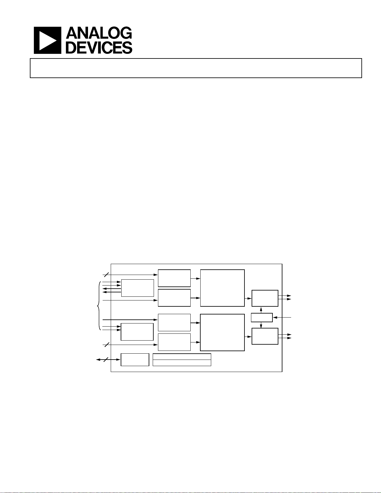
FUNCTIONAL BLOCK DIAGRAM
SERIAL
INPUTA
CLOCK
SIGNAL
GROUP
SERIAL
INPUT B
SPI I/O
GROUP
3
PLL DIVIDERS
PLL DIVIDERS
3
4
SPI PORT
SERIAL
INPUT
CLOCK
DOUBLER
CLOCK
DOUBLER
SERIAL
INPUT
CONTROL REGISTERS
PARAMETER RAM
Figure 1. Functional Block Diagram
BTSC
ENCODER
CORE A
BTSC
ENCODER
CORE B
DAC
BIAS
DAC
AD71028
ENCODED
OUTPUT A
ANALOG
ENCODED
OUTPUT B
04482-0-001
BTSC
BIAS
BTSC
Rev. 0
Information furnished by Analog Devices is believed to be accurate and reliable.
However, no responsibility is assumed by Analog Devices for its use, nor for any
infringements of patents or other rights of third parties that may result from its use.
Specifications subject to change without notice. No license is granted by implication
or otherwise under any patent or patent rights of Analog Devices. Trademarks and
registered trademarks are the property of their respective owners.
One Technology Way, P.O. Box 9106, Norwood, MA 02062-9106, U.S.A.
Tel: 781.329.4700 www.analog.com
Fax: 781.326.8703 © 2004 Analog Devices, Inc. All rights reserved.

AD71028
TABLE OF CONTENTS
Specifications..................................................................................... 3
DAC Analog Performance........................................................... 3
BTSC Encoder Performance ....................................................... 3
Digital I/O ..................................................................................... 3
Power.............................................................................................. 4
Temperature Range ...................................................................... 4
Digital Timing............................................................................... 4
Absolute Maximum Ratings............................................................ 5
Pin Configuration and Functional Descriptions.......................... 6
Features .............................................................................................. 8
Pin Functions ................................................................................ 8
Signal Processing ............................................................................ 10
Background of BTSC ................................................................. 10
Performance Factors .................................................................. 10
Separation Alignment................................................................ 10
Input Levels ................................................................................. 11
Clock Relationships.................................................................... 11
SPI Port ............................................................................................ 12
Overview ..................................................................................... 12
SPI Address Decoding ............................................................... 12
Parameter RAM.......................................................................... 13
Control Register ......................................................................... 13
Output Level Register ................................................................ 13
Stereo Enhancement Register................................................... 13
Dialog Enhancement Register.................................................. 13
SPI Read/Write Data Formats .................................................. 14
Initialization ................................................................................ 14
Serial Data Input Port................................................................ 14
Analog Output Section .................................................................. 16
Outline Dimensions....................................................................... 17
Phase Linearity of the External Analog Filter......................... 11
REVISION HISTORY
Revision 0: Initial Version
Ordering Guide .......................................................................... 17
Rev. 0 | Page 2 of 20

AD71028
SPECIFICATIONS
TEST CONDITIONS, UNLESS OTHERWISE NOTED
Supply Voltages (AV
, DVDD) 5.0 V
DD
Ambient Temperature 25°C
Input Clock 12.288 MHz
Input Signal 1 kHz, 0 dBFS
Input Sample Rate 48 kHz
Measurement Bandwidth 20 Hz to 14 kHz
Word Width 24 Bits
Load Capacitance 50 pF
Input Voltage HI 2.4 V
Input Voltage LO 0.4 V
DAC ANALOG PERFORMANCE
Table 1.
Parameter Min Typ Max Unit
Resolution 24 Bits
Dynamic Range (20 Hz to 14 kHz, –60 dB Input) (Encoded Output, Left = Right) 85 921 dB
Total Harmonic Distortion + Noise (Encoded Output, Left = Right, 20 Hz to 14 kHz)
VIN = 0 dB –85 –921 dB
Differential Output Range (± Full Scale, Left = Right) 1.7 V p-p
1
Measurement of encoded BTSC signal, not a measurement of end-to-end system.
BTSC ENCODER PERFORMANCE
Table 2.
Parameter Min Typ Max Unit
Channel Separation
1
30 Hz to 500 Hz 27 dB
500 Hz to 5 kHz 23 dB
5 kHz to 13.5 kHz 16 dB
Frequency Response1
30 Hz to 10 kHz +0.5 –1.0 dB
30 Hz to 13.5 kHz +0.5 –1.5 dB
1
These specifications are measured with a –25 dB, 1 kHz input signal.
DIGITAL I/O
Table 3.
Parameter Min Typ Max Unit
Input Voltage HI (VIH) 2.1 V
Input Voltage LO (VIL) 0.8 V
Input Leakage (IIH @ VIH = 2.4 V) 10 µA
Input Leakage (IIL @ VIL = 0.8 V) 10 µA
High Level Output Voltage (VOH) IOH = 2 mA DVDD – 0.5 V
Low Level Output Voltage (VOL) IOL = 2 mA 0.4 V
Rev. 0 | Page 3 of 20

AD71028
POWER
Table 4.
Parameter Min Typ Max Unit
Supplies
Voltage, Analog and Digital 4.5 5 5.5 V
Analog Current 31 37 mA
Digital Current 97 110 mA
Dissipation
Operation—Both Supplies 640 mW
Operation—Analog Supplies 155 mW
Operation—Digital Supplies 485 mW
TEMPERATURE RANGE
Table 5.
Parameter Min Typ Max Unit
Specifications Guaranteed 25 °C
Functionality Guaranteed 0 70 °C
Storage –55 +125 °C
DIGITAL TIMING
Table 6.
Parameter Min Typ Max Unit
t
t
t
t
t
t
t
t
t
t
t
t
t
t
t
DMD
DBL
DBH
DLS
DLH
DDS
DDH
CCL
CCH
CLS
CLH
CLD
CDS
CDH
RLP
MCLK Recommended Duty Cycle @ 12.288 MHz (256 × fS and 512 × fS Modes) 40 60 %
BCLK Low Pulse Width 25 ns
BCLK High Pulse Width 10 ns
LRCLK Setup 0 ns
LRCLK Hold 10 ns
SDATA Setup 0 ns
SDATA Hold 10 ns
CCLK Low Pulse Width 10 ns
CCLK High Pulse Width 10 ns
CLATCH Setup 10 ns
CLATCH Hold 20 ns
CLATCH High Pulse Width 10 ns
CDATA Setup 0 ns
CDATA Hold 10 ns
Reset LO Pulse Width 10 ns
Rev. 0 | Page 4 of 20

AD71028
ABSOLUTE MAXIMUM RATINGS
Table 7. AD71028 Stress Ratings
Parameter Min Max Unit
DVDD to DGND –0.3 +6 V
ODVDD to DGND –0.3 +6 V
AVDD to AGND –0.3 +6 V
Digital Inputs DGND – 0.3 DVDD + 0.3 V
Analog Inputs AGND – 0.3 AVDD + 0.3 V
AGND to DGND –0.3 +0.3 V
Reference Voltage (AVDD + 0.3)/2 V
Maximum Junction
Temperature
Storage Temperature
Range –65 +150 °C
Soldering 300 °C
10 sec
125 °C
Table 8. Package Characteristics (48-Lead LQFP)
Parameter Min Typ Max Unit
θJA Thermal Resistance
[Junction-to-Ambient]
θJC Thermal Resistance
[Junction-to-Case]
72 °C/W
19.5 °C/W
Stresses above those listed under Absolute Maximum Ratings
may cause permanent damage to the device. This is a stress
rating only; functional operation of the device at these or any
other conditions above those listed in the operational sections
of this specification is not implied. Exposure to absolute
maximum rating conditions for extended periods may affect
device reliability.
ESD CAUTION
ESD (electrostatic discharge) sensitive device. Electrostatic charges as high as 4000 V readily accumulate on
the human body and test equipment and can discharge without detection. Although this product features
proprietary ESD protection circuitry, permanent damage may occur on devices subjected to high energy
electrostatic discharges. Therefore, proper ESD precautions are recommended to avoid performance
degradation or loss of functionality.
Rev. 0 | Page 5 of 20

AD71028
A
PIN CONFIGURATION AND FUNCTIONAL DESCRIPTIONS
FILTCAP
REFCAP
NC
38 37
22
23
24
BCLK_PB
LRCLK_PB
SDATA_PB
DIV2_P
DIV1_PB
DIV2_PB
NC
NC
DGND
DVDD
ODVDD
NC
NC
COUT
CDATA
DIV1_PA
48 47 46 45 44
1
2
3
4
5
6
7
8
9
10
11
12
13
DVDD
14
MCLK_PB
15
CCLK
PLL_PB
DVDD
(Not to Scale)
16
DGND
CLATCH
DGND
MCLK_PA
PLL_PA
43 42 41 40 39
AD71028
TOP VIEW
17
18
19
DVDD
RESETB
SDATA_PA
CLK27_PB
CLK27_PA
20
21
BCLK_PA
LRCLK_PA
36
35
34
33
32
31
30
29
28
27
26
25
AGND
OUTB–
OUTB+
AVDD
AGND
AVDD
OUTA+
OUTA–
AGND
NC
NC
DOUBLE
04482-0-002
NC = NO CONNECT
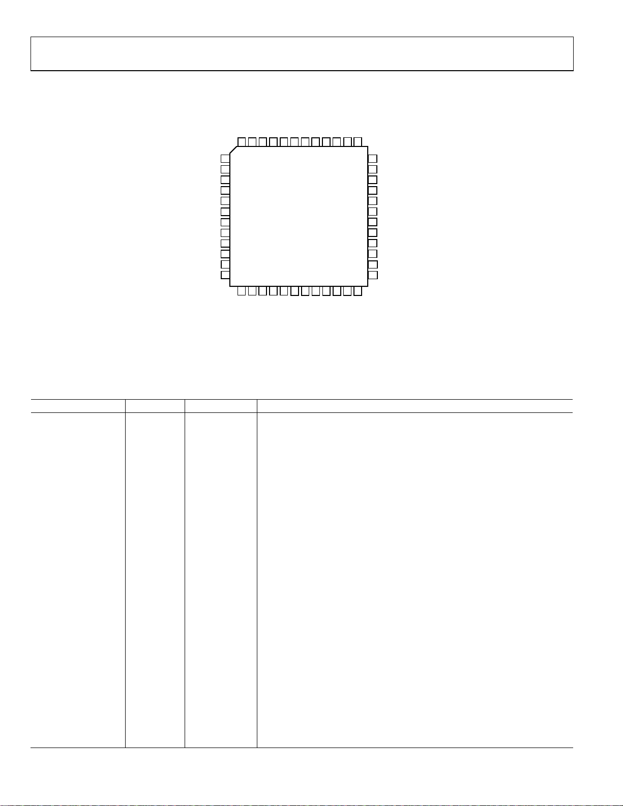
Figure 2. 48-Lead Low Profile Quad Flat Pack (LQFP)
Table 9. Pin Function Descriptions
Pin No. Mnemonic Input/Output Description
1 DIV2_PA OUT CLK27_PA clock (Pin 40) Divided by 1125
2 DIV1_PB OUT PLL_PB Clock (Pin 46) Divided by 512 (DOUBLE = 1) or 1024 (DOUBLE = 0)
3 DIV2_PB OUT CLK27_PB Clock (Pin 41) Divided by 1125
4, 5, 9, 10, 26, 27, 39 NC No Connection
6, 16, 44 DGND Digital Ground
7, 13, 17, 45 DVDD Digital Supply for DSP Core
8 ODVDD Digital Supply for Output Buffers
11 COUT OUT SPI Readback
12 CDATA IN SPI Control Data Input
14 CCLK IN SPI Serial Bit Clock
15 CLATCH IN SPI Control Latch Signal
18 RESETB IN Reset Signal for Both Processors, Active Low
19 SDATA_PA IN Data Input to Processor A
20 BCLK_PA IN Bit Clock Signal for Serial Data Input to Processor A
21 LRCLK_PA IN Left/Right Framing Signal for Data Input to Processor A
22 SDATA_PB IN Data Input to Processor B
23 BCLK_PB IN Bit Clock Signal for Serial Data Input to Processor B
24 LRCLK_PB IN Left/Right Framing Signal for Data Input to Processor B
25 DOUBLE IN Enables Internal Clock Doubler for 12.288 MHz Input (Both Processors)
28, 32, 36 AGND Analog Ground
29 OUTA– OUT Negative Analog Output, Processor A
30 OUTA+ OUT Positive Analog Output, Processor A
31, 33 AVDD Analog Supply
34 OUTB+ OUT Positive Analog Output, Processor B
35 OUTB– OUT Negative Analog Output, Processor B
37 REFCAP IN Connection Point for 10 µF VREF Filter Capacitor
38 FILTCAP IN Connection for Noise Reduction Capacitor
Rev. 0 | Page 6 of 20
 Loading...