Analog Devices AD708BQ, AD708BH, AD708AQ, AD708AH, AD708SQ Datasheet
...
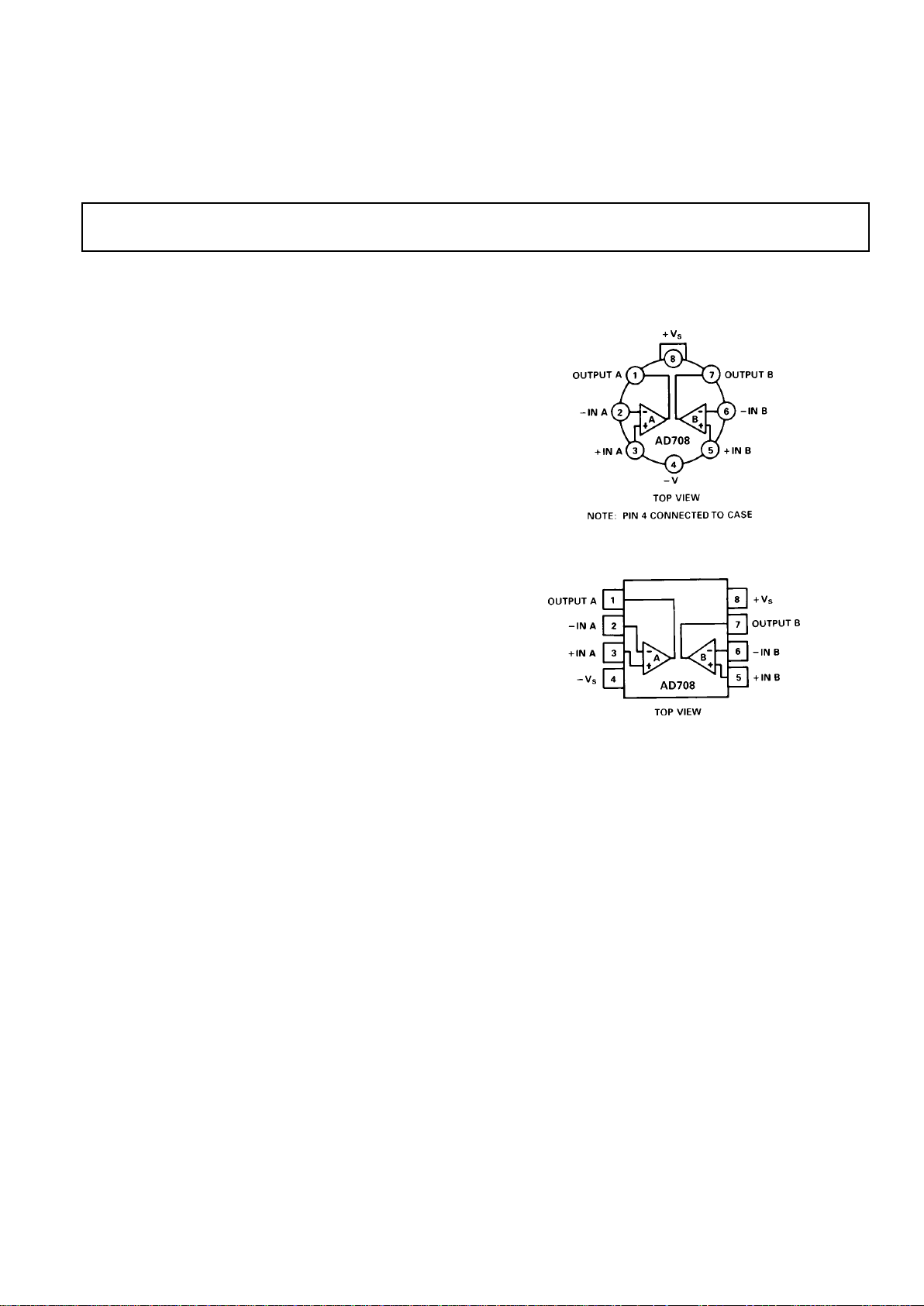
CONNECTION DIAGRAMS
TO-99 (H) Package
Plastic (N ), and Cerdip (Q) Packages
REV. B
Information furnished by Analog Devices is believed to be accurate and
reliable. However, no responsibility is assumed by Analog Devices for its
use, nor for any infringements of patents or other rights of third parties
which may result from its use. No license is granted by implication or
otherwise under any patent or patent rights of Analog Devices.
a
Ultralow Offset Voltage
Dual Op Amp
AD708
One Technology Way, P.O. Box 9106, Norwood, MA 02062-9106, U.S.A.
Tel: 617/329-4700 Fax: 617/326-8703
FEATURES
Very High DC Precision
30 mV max Offset Voltage
0.3 mV/8C max Offset Voltage Drift
0.35 mV p-p max Voltage Noise (0.1 Hz to 10 Hz)
5 Million V/V min Open Loop Gain
130 dB min CMRR
120 dB min PSRR
Matching Characteristics
30 mV max Offset Voltage Match
0.3 mV/8C max Offset Voltage Drift Match
130 dB min CMRR Match
Single Version: AD707
Available in 8-Pin Plastic Mini-DIP,
Hermetic Cerdip and TO-99 Metal Can
Packages, Chips and /883B Parts Available.
PRODUCT DESCRIPTION
The AD708 is a very high precision, dual monolithic operational
amplifier. Each amplifier individually offers excellent dc precision
with the best available max offset voltage and offset voltage drift
of any dual bipolar op amp. In addition, the matching specifications are the best available in any dual op amp.
The AD708 sets a new standards for dual precision op amps by
providing 5 V/µV min open loop gain and guaranteed max input
voltage noise of 350 nV p-p (0.1 Hz to 10 Hz). All dc specifications show excellent stability over temperature, with offset
voltage drift typically 0.1 µV/°C and input bias current drift of
25 pA/°C max. Both CMRR (130 dB min) and PSRR (120 dB
min) are an order of magnitude improved over any available
single monolithic op amp except the AD707.
The AD708 is available in four performance grades. The
AD708J is rated over the commercial temperature range of 0°C
to +70°C and jis available in a plastic mini-DIP package. The
AD708A and AD708B are rated over the industrial temperature
range of –40°C to +85°C and are available in a cerdip and TO99 package. The AD708S is rated over the military temperature
range of –55°C to +125°C and is available in cerdip and TO-99
packages. Military versions are available processed to MILSTD-883B, Rev. C.
APPLICATION HIGHLIGHTS
1. The combination of outstanding matching and individual
specifications make the AD708 ideal for constructing high
gain, precision instrumentation amplifiers.
2. The low offset voltage drift and low noise of the AD708
allows the designer to amplify very small signals without
sacrificing overall system performance.
3. The AD708’s 10 V/µV typical open loop gain and 140 dB
common-mode rejection make it ideal for precision
applications.
4. Unmounted dice are available for hybrid circuit applications.
5. The AD708 is an improved replacement for the LT1002.

AD708–SPECIFICATIONS
(@ +258C and 615 V dc, unless otherwise noted)
–2–
REV. B
AD708J/A AD708B AD708S
Model Conditions Min Typ Max Min Typ Max Min Typ Max Units
INPUT OFFSET VOLTAGE
1
30 100 5 50 5 30 µV
T
MIN
to T
MAX
50 150 15 65 15 50 µV
Drift 0.3 1.0 0.1 0.4 0.1 0.3 µV/°C
Long Term Stability 0.3 0.3 0.3 µV/Month
INPUT BIAS CURRENT 1.0 2.5 0.5 1.0 0.5 1 nA
T
MIN
to T
MAX
2.0 4.0 1.0 2.0 1.0 4 nA
Average Drift 15 40 10 25 10 30 pA/°C
OFFSET CURRENT V
CM
= 0 V 0.5 2.0 0.1 1.0 0.1 1 nA
T
MIN
to T
MAX
2.0 4.0 0.2 1.5 0.2 1.5 nA
Average Drift 2 60 1 25 1 25 pA/°C
MATCHING CHARACTERISTICS
2
Offset Voltage 80 50 30 µV
T
MIN
to T
MAX
150 75 50 µV
Offset Voltage Drift 1.0 0.4 0.3 µV/°C
Input Bias Current 4.0 1.0 1.0 nA
T
MIN
to T
MAX
5.0 2.0 2.0 nA
Common-Mode Rejection 120 140 130 140 130 140 dB
T
MIN
to T
MAX
110 130 130 dB
Power Supply Rejection 110 120 120 dB
T
MIN
to T
MAX
110 120 120 dB
Channel Separation 135 140 140 dB
INPUT VOLTAGE NOISE 0.1 Hz to 10 Hz 0.23 0.6 0.23 0.6 0.23 0.35 µV p-p
f = 10 Hz 10.3 18 10.3 12 10.3 12 nV/√
Hz
f = 100 Hz 10.0 13.0 10.0 11.0 10.0 11 nV/√
Hz
f = 1 kHz 9.6 11.0 9.6 11.0 9.6 11 nV/√Hz
INPUT CURRENT NOISE 0.1 Hz to 10 Hz 14 35 14 35 14 35 pA p-p
f = 10 Hz 0.32 0.9 0.32 0.8 0.32 0.8 pA/√
Hz
f = 100 Hz 0.14 0.27 0.14 0.23 0.14 0.23 pA/√
Hz
f = 1 kHz 0.12 0.18 0.12 0.17 0.12 0.17 pA/√Hz
COMMON-MODE
REJECTION RATIO V
CM
= ±13 V 120 140 130 140 130 140 dB
T
MIN
to T
MAX
120 140 130 140 130 140 dB
OPEN-LOOP GAIN V
O
= ±10 V
R
LOAD
≥ 2 kΩ 3 10 5 10 4 10 V/µV
T
MIN
to T
MAX
310 510 47V/µV
POWER SUPPLY
REJECTION RATIO V
S
= ±3 V to ±18 V 110 130 120 130 120 130 dB
T
MIN
to T
MAX
110 130 120 130 120 130 dB
FREQUENCY RESPONSE
Closed Loop Bandwidth 0.5 0.9 0.5 0.9 0.5 0.9 MHz
Slew Rate 0.15 0.3 0.15 0.3 0.15 0.3 V/µs
INPUT RESISTANCE
Differential 60 200 200 MΩ
Common Mode 200 400 400 GΩ
OUTPUT VOLTAGE R
LOAD
≥ 10 kΩ 13.5 14 13.5 14.0 13.5 14 ±V
R
LOAD
≥ 2 kΩ 12.5 13.0 12.5 13.0 12.5 13 ±V
R
LOAD
≥ 1 kΩ 12.0 12.5 12.0 12.5 12.0 12.5 ±V
R
LOAD
≥ 2 kΩ
T
MIN
to T
MAX
12.0 13.0 12.0 13.0 12.0 13 ±V
OPEN-LOOP OUTPUT
RESISTANCE 60 60 60 Ω

AD708J/A AD708B AD708S
Model Conditions Min Typ Max Min Typ Max Min Typ Max Units
POWER SUPPLY
Quiescent Current 4.5 5.5 4.5 5.5 4.5 5.5 mA
Power Consumption V
S
= ±15 V
No Load 135 165 135 165 135 165 mW
V
S
= ±3 V 12 18 12 18 12 18 mW
Operating Range ±3 ±18 ±3 ± 18 ±3 ±18 V
NOTES
1
Input offset voltage specifications are guaranteed after 5 minutes of operation at TA = +25°C.
2
Matching is defined as the difference between parameters of the two amplifiers.
All min and max specifications are guaranteed. Specifications in boldface are tested on all production units at final electrical test. Results from those tests are used to
calculate outgoing quality levels.
Specifications subject to change without notice.
ABSOLUTE MAXIMUM RATINGS
1
Supply Voltage . . . . . . . . . . . . . . . . . . . . . . . . . . . . . . . . ±22 V
Internal Power Dissipation
2
Input Voltage3 . . . . . . . . . . . . . . . . . . . . . . . . . . . . . . . . . ±V
S
Output Short Circuit Duration . . . . . . . . . . . . . . . . Indefinite
Differential Input Voltage . . . . . . . . . . . . . . . . . . +V
S
and –V
S
Storage Temperature Range (Q, H) . . . . . . . –65°C to +150°C
Storage Temperature Range (N) . . . . . . . . . –65°C to +125°C
Lead Temperature Range (Soldering 60 sec) . . . . . . . . +300°C
NOTES
1
Stresses above those listed under “Absolute Maximum Ratings” may cause
permanent damage to the device. This is a stress rating only and functional
operation of the device at these or any other conditions above those indicated in
the operational section of this specification is not implied. Exposure to absolute
maximum rating conditions for extended periods may affect device reliability.
2
Thermal Characteristics
8-Pin Plastic Package: θJC = 33°C/Watt, θJA = 100°C/Watt
8-Pin Cerdip package: θJC = 30°C/Watt, θJA = 110°C/Watt
8-Pin Metal Can Package: θJC = 65°C/Watt, θJA = 150°C/Watt.
3
For supply voltages less than ±22 V, the absolute maximum input voltage is
equal to the supply voltage.
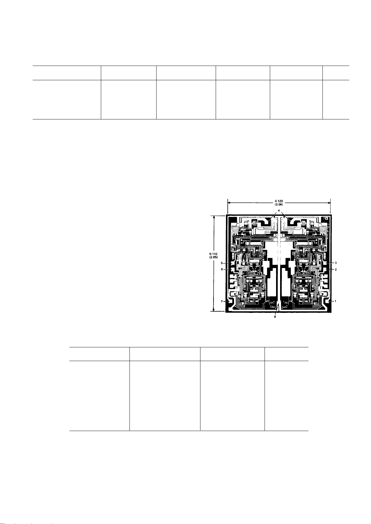
METALIZATION PHOTOGRAPH
Dimensions shown in inches and (mm).
Contact factory for latest dimensions.
REV. B
–3–
AD708
ORDERING GUIDE
Temperature Package Package
Model Range Description Option*
AD708JN 0°C to +70°C 8-Pin Plastic DIP N-8
AD708AQ –40°C to +85°C 8-Pin Cerdip Q-8
AD708BQ –40°C to +85°C 8-Pin Cerdip Q-8
AD708SQ –55°C to +125°C 8-Pin Cerdip Q-8
AD708AH –40°C to +85°C 8-Pin Header H-08A
AD708BH –40°C to +85°C 8-Pin Header H-08A
AD708SH –55°C to +125°C 8-Pin Header H-08A
AD708SH/883B –55°C to +125°C 8-Pin Header H-08A
AD708J Grade Chips 0°C to +70°C Die
AD708S Grade Chips –55°C to +125°C Die
*N = Plastic DIP; Q = Cerdip; H = Hermetic Metal Can.
 Loading...