High Precision,
www.BDTIC.com/ADI
FEATURES
Laser-trimmed to high accuracy: 2.500 V ±0.4%
3-terminal device: voltage in/voltage out
Excellent temperature stability: 10 ppm/°C (AD580M, U)
Excellent long-term stability: 250 µV (25 µV/month)
Low quiescent current: 1.5 mA maximum
Small, hermetic IC package: TO-52 can
MIL-STD-883 compliant versions available
GENERAL DESCRIPTION
The AD5801 is a 3-terminal, low cost, temperaturecompensated, bandgap voltage reference, which provides a fixed
2.5 V output for inputs between 4.5 V and 30 V. A unique
combination of advanced circuit design and laser-wafer
trimmed thin film resistors provide the AD580 with an initial
tolerance of ±0.4%, a temperature stability of better than 10
ppm/°C, and long-term stability of better than 250 µV. In
addition, the low quiescent current drain of 1.5 mA maximum
offers a clear advantage over classical Zener techniques.
The AD580 is recommended as a stable reference for all 8-, 10-,
and 12-bit D/A converters that require an external reference. In
addition, the wide input range of the AD580 allows operation
with 5 volt logic supplies, making the AD580 ideal for digital
panel meter applications or whenever only a single logic power
supply is available.
The AD580J, K, L, and M are specified for operation over the
0°C to +70°C temperature range; the AD580S, T, and U are
specified for operation over the extended temperature range of
–55°C to +125°C.
2.5 V IC Reference
AD580
FUNCTIONAL BLOCK DIAGRAM
+E
E
–E
Figure 1.
OUT
00525-B-001
BOTTOM
VIEW
PRODUCT HIGHLIGHTS
1. Laser-trimming of the thin film resistors minimizes the
AD580 output error. For example, the AD580L output
tolerance is ±10 mV.
2. The three-terminal voltage in/voltage out operation of the
AD580 provides regulated output voltage without any
external components.
3. The AD580 provides a stable 2.5 V output voltage for input
voltages between 4.5 V and 30 V. The capability to provide
a stable output voltage using a 5 V input makes the AD580
an ideal choice for systems that contain a single logic
power supply.
4. Thin film resistor technology and tightly controlled bipolar
processing provide the AD580 with temperature stabilities
to 10 ppm/°C and long-term stability better than 250 µV.
5. The low quiescent current drain of the AD580 makes it
ideal for CMOS and other low power applications.
6. The AD580 is available in versions compliant with MIL-
STD-883. Refer to the Analog Devices Military Products
Data Book or the current AD580/AD883B data sheet for
detailed specifications.
1
Protected by U.S. Patent Numbers 3,887,863; RE30,586.
Rev. B
Information furnished by Analog Devices is believed to be accurate and reliable.
However, no responsibility is assumed by Analog Devices for its use, nor for any
infringements of patents or other rights of third parties that may result from its use.
Specifications subject to change without notice. No license is granted by implication
or otherwise under any patent or patent rights of Analog Devices. Trademarks and
registered trademarks are the property of their respective owners.
One Technology Way, P.O. Box 9106, Norwood, MA 02062-9106, U.S.A.
Tel: 781.329.4700 www.analog.com
Fax: 781.326.8703 © 2004 Analog Devices, Inc. All rights reserved.

AD580
www.BDTIC.com/ADI
TABLE OF CONTENTS
Specifications..................................................................................... 3
The AD580 as a Current Limiter.................................................6
Absolute Maximum Ratings............................................................ 4
AD580 Chip Dimensions And Pad Layout............................... 4
ESD Caution.................................................................................. 4
Theory of Operation ........................................................................ 5
Voltage Variation versus Temperature ....................................... 5
Noise Performance ....................................................................... 6
REVISION HISTORY
8/04—Changed from Rev. A to Rev. B
Updated Format................................................................ Universal
The AD580 as a Low Power, Low Voltage, Precision Reference
for Data Converters.......................................................................7
Outline Dimensions..........................................................................8
Ordering Guide .............................................................................8
Rev. B | Page 2 of 8

AD580
www.BDTIC.com/ADI
SPECIFICATIONS
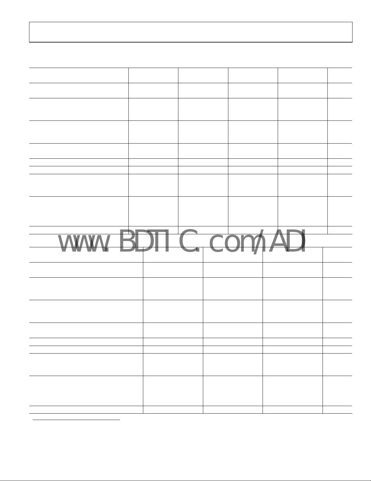
Table 1. VIN = 15 V and 25°C
AD580J AD580K AD580L AD580M
Model Min Typ Max Min Typ Max Min Typ Max Min Typ Max Units
OUTPUT VOLTAGE TOLERANCE
Error from Nominal 2.500 V Output ±75 ±25 ±10 ±10 mV
OUTPUT VOLTAGE CHANGE
T
to T
MIN
85 40 25 10 ppm/°C
LINE REGULATION
7 V ≤ VIN ≤ 30 V 1.5
4.5 V ≤ VIN ≤ 7 V 0.3
LOAD REGULATION
∆I = 10 mA
QUIESCENT CURRENT 1.0
NOISE (0.1 Hz to 10 Hz) 8 8 8 8 µV p-p
STABILITY
Long Term 250 250 250 250 µV
Per Month 25 25 25 25 µV
TEMPERATURE PERFORMANCE
Specified 0 +70 0 +70 0 +70 0 +70 °C
Operating –55 +125 –55 +125 –55 +125 –55 +125 °C
Storage –65 +175 –65 +175 –65 +175 –65 +175 °C
PACKAGE OPTION2 TO-52 (H-03A) AD580JH AD580KH AD580LH AD580MH
Table 2.
AD580S AD580T AD580U
Model Min Typ Max Min Typ Max Min Typ Max Units
OUTPUT VOLTAGE TOLERANCE
Error from Nominal 2.500 V Output
OUTPUT VOLTAGE CHANGE
T
MIN
55 25 10 ppm/°C
LINE REGULATION
7 V ≤ VIN ≤ 30 V 1.5
4.5 V ≤ VIN ≤ 7 V 0.3
LOAD REGULATION
∆I = 10 mA
QUIESCENT CURRENT 1.0
NOISE (0.1 Hz to 10 Hz) 8 8 8 µV p-p
STABILITY
Long Term 250 250 250 µV
Per Month 25 25 25 µV
TEMPERATURE PERFORMANCE
Specified –55 +125 –55 +125 –55 +125 °C
Operating –55 +150 –55 +150 –55 +150 °C
Storage –65 +175 –65 +175 –65 +175 °C
PACKAGE OPTION2 TO-52 (H-03A) AD580SH AD580TH AD580UH
1
Specifications shown in boldface are tested on all production units at final electrical test. Results from those tests are used to calculate outgoing quality levels. All min
and max specifications are guaranteed, although only those shown in boldface are tested on all production units.
2
H = Metal Can.
15 7 4.3 1.75 mV
MAX
1
to T
MAX
6
3
10
1.5
1.5 4
0.3 2
1.0
±251
25
6
3
10
1.5
10
1.5
1.0
1.0
±10
11
2
1
10
1.5
2
1
10
1.5
1.0
1.0
±10
4.5
2
1
10
1.5
2
1
10
1.5
mV
mV
mV
mA
mV
mV
mV
mV
mV
mA
Rev. B | Page 3 of 8
 Loading...