


System Ready, 18-Bit ±1 LSB INL,
VCCV
V
Data Sheet
FEATURES
True 18-bit voltage output DAC, ±1 LSB INL
8 nV/√Hz output noise spectral density
0.025 LSB long-term linearity error stability
±0.018 ppm/°C gain error temperature coefficient
2.5 μs output voltage settling time
3.5 nV-sec midscale glitch impulse
Integrated precision reference buffers
Operating temperature range: −40°C to +125°C
4 mm × 5 mm LFCSP package
Wide power supply range of up to ±16.5 V
35 MHz Schmitt triggered digital interface
1.8 V-compatible digital interface
APPLICATIONS
Medical instrumentation
Test and measurement
Industrial control
Scientific and aerospace instrumentation
Data acquisition systems
Digital gain and offset adjustment
Power supply control
Voltage Output DAC
AD5780
FUNCTIONAL BLOCK DIAGRAM
DD
IOV
SDIN
SCLK
SYNC
SDO
LDAC
CLR
RESET
CC
DGND
AD5780
INPUT
SHIFT
REGISTE R
CONTROL
LOGIC
POWER-ON RESET
AND CLEAR LOG IC
18
AND
SS
AGNDV
Table 1. Related Devices
Part No. Description
AD5790 20-bit, 2 LSB accurate DAC
AD5791 20-bit, 1 ppm accurate DAC
AD5781 18-bit, 0.5 LSB accurate DAC
AD5541A/AD5542A 16-bit, 1 LSB accurate 5 V DAC
AD5760 16-bit, 0.5 LSB accurate DAC
DAC
REG
REFP
18
Figure 1.
18-BIT
DAC
V
REFN
R1
6.8kΩ
A1
6kΩ
R
FB
6.8kΩ
R
INV
V
FB
OUT
09649-001
GENERAL DESCRIPTION
The AD57801 is a true 18-bit, unbuffered voltage output DAC
that operates from a bipolar supply of up to 33 V. The AD5780
accepts a positive reference input range of 5 V to V
and a negative reference input range of V
+ 2.5 V to 0 V. Both
SS
reference inputs are buffered on chip and external buffers are
not required. The AD5780 offers a relative accuracy specification of ±1 LSB maximum range, and operation is guaranteed
monotonic with a ±1 LSB DNL maximum range specification.
The part uses a versatile 3-wire serial interface that operates at
clock rates of up to 35 MHz and is compatible with standard
SPI, QSPI™, MICROWIRE™, and DSP interface standards. The
part incorporates a power-on reset circuit that ensures that the
DAC output powers up to 0 V in a known output impedance
state and remains in this state until a valid write to the device
takes place. The part provides an output clamp feature that
places the output in a defined load state.
1
Protected by U.S. Patent No. 7,884,747 and 8,089,380.
− 2.5 V
DD
PRODUCT HIGHLIGHTS
1. True 18-bit accuracy.
2. Wide power supply range of up to ±16.5 V.
3. −40°C to +125°C operating temperature range.
4. Low 8 nV/√Hz noise.
5. Low ±0.018 ppm/°C gain error temperature coefficient.
COMPANION PRODUCTS
Output Amplifier Buffer: AD8675, ADA4898-1, ADA4004-1
External Reference: ADR445
DC-to-DC Design Tool: ADIsimPower™
Additional companion products on the AD5780 product page
Rev. C
Information furnished by Analog Devices is believed to be accurate and reliable. However, no
responsibility is assumed by Anal og Devices for its use, nor for any infringements of patents or ot her
rights of third parties that may result from its use. Specifications subject to change without notice. No
license is granted by implication or otherwise under any patent or patent rights of Analog Devices.
Trademarks and registered trademarks are the property of their respective owners.
One Technology Way, P.O. Box 9106, Norwood, MA 02062-9106, U.S.A.
Tel: 781.329.4700 www.analog.com
Fax: 781.461.3113 ©2011–2012 Analog Devices, Inc. All rights reserved.

AD5780 Data Sheet
TABLE OF CONTENTS
Features.............................................................................................. 1
Applications....................................................................................... 1
Functional Block Diagram ..............................................................1
General Description......................................................................... 1
Product Highlights........................................................................... 1
Companion Products....................................................................... 1
Revision History ...............................................................................2
Specifications..................................................................................... 3
Timing Characteristics ................................................................ 5
Absolute Maximum Ratings............................................................ 8
ESD Caution.................................................................................. 8
Pin Configuration and Function Descriptions............................. 9
Typical Performance Characteristics........................................... 10
Terminology .................................................................................... 18
Theory of Operation ......................................................................19
DAC Architecture....................................................................... 19
Serial Interface............................................................................ 19
Hardware Control Pins.............................................................. 20
On-Chip Registers...................................................................... 21
AD5780 Features............................................................................ 24
Power-On to 0 V......................................................................... 24
Configuring the AD5780 .......................................................... 24
DAC Output State ...................................................................... 24
Output Amplifier Configuration.............................................. 24
Applications Information.............................................................. 26
Typical Operating Circuit ......................................................... 26
Evaluation Board........................................................................ 27
Outline Dimensions....................................................................... 28
Ordering Guide .......................................................................... 28
REVISION HISTORY
3/12—Rev. B to Rev. C
Changes to Data Sheet Title and added Patent 8,089,380........... 1
2/12—Rev. A to Rev. B
Deleted Linearity Compensation Section ................................... 24
12/11—Rev. 0 to Rev. A
Edits to Table 2.................................................................................. 3
Changes to Figure 48...................................................................... 17
Changes to DAC Register Section................................................ 21
Changes to Table 10 and Table 11 ................................................ 22
11/11—Revision 0: Initial Version
Rev. C | Page 2 of 28

Data Sheet AD5780
SPECIFICATIONS
VDD = 12.5 V to 16.5 V, VSS = −16.5 V to −12.5 V, V
R
= unloaded, CL = unloaded, T
L
MIN
to T
, unless otherwise noted.
MAX
= 10 V, V
REFP
= −10 V, VCC = 2.7 V to 5.5 V, IOVCC = 1.71 V to 5.5 V,
REFN
Table 2.
A, B Versions
1
Parameter Min Typ Max Unit Test Conditions/Comments
STATIC PERFORMANCE2
Resolution 18 Bits
Integral Nonlinearity Error (Relative
Accuracy)
−1 +1 LSB B grade, V
−2 +2 LSB A grade, V
Differential Nonlinearity Error −0.25 +0.75 LSB B grade, V
−1 +1 LSB A grade, V
−0.85 +0.85 LSB B grade, V
= 25°C
T
A
= +10 V, V
REFP
= ±10 V, +10 V, and +5 V
REFx
= ±10 V, +10 V, and +5 V
REFx
= ±10 V, +10 V, and +5 V
REFx
= ±10 V, +10 V, and +5 V
REFx
= −10 V,
REFN
Long-Term Linearity Error Stability3 0.025 LSB After 750 hours at TA = 135°C
Full-Scale Error −3 ±0.95 +3 LSB V
−5.5 ±0.675 +0.5 LSB V
−10 ±0.45 +10 LSB V
Full-Scale Error Temperature Coefficient ±0.026 ppm/°C V
Zero-Scale Error −4.8 ±0.325 +4.8 LSB V
−10 ±0.175 +10 LSB V
−20.5 ±0.225 +20.5 LSB V
Zero-Scale Error Temperature
±0.025 ppm/°C V
= +10 V, V
REFP
= 10 V, V
REFP
= 5 V, V
REFP
= +10 V, V
REFP
= +10 V, V
REFP
= 10 V, V
REFP
= 5 V, V
REFP
= +10 V, V
REFP
REFN
REFN
REFN
REFN
= 0 V
REFN
REFN
REFN
= 0 V
REFN
= −10 V
= 0 V
= −10 V
= −10 V
= 0 V
= −10 V
Coefficient
Gain Error −19 ±2.3 +19 ppm FSR V
−35 ±1.9 +35 ppm FSR V
−68 ±0.9 +68 ppm FSR V
Gain Error Temperature Coefficient ±0.018 ppm/°C V
= +10 V, V
REFP
= 10 V, V
REFP
= 5 V, V
REFP
= +10 V, V
REFP
REFN
REFN
REFN
= 0 V
REFN
= −10 V
= 0 V
= −10 V
R1, RFB Matching 0.015 %
OUTPUT CHARACTERISTICS
Output Voltage Range V
Output Voltage Settling Time 2.5 μs
V
REFN
REFP
V
10 V step to 0.02%, using the ADA4898-1
buffer in unity-gain mode
3.5 μs 500 code step to ±1 LSB4
Output Noise Spectral Density 8 nV/√Hz At 1 kHz, DAC code = midscale
8 nV/√Hz At 10 kHz, DAC code = midscale
Output Voltage Noise 1.1 μV p-p
DAC code = midscale, 0.1 Hz to
10 Hz bandwidth
Midscale Glitch Impulse4 14 nV-sec V
3.5 nV-sec V
4 nV-sec V
MSB Segment Glitch Impulse4 14 nV-sec V
3.5 nV-sec V
4 nV-sec V
= +10 V, V
REFP
= 10 V, V
REFP
= 5 V, V
REFP
= +10 V, V
REFP
= 10 V, V
REFP
= 5 V, V
REFP
= −10 V
REFN
= 0 V
REFN
= 0 V
REFN
= −10 V, see Figure 43
REFN
= 0 V, see Figure 44
REFN
= 0 V, see Figure 45
REFN
Output Enabled Glitch Impulse 57 nV-sec On removal of output ground clamp
Digital Feedthrough 0.27 nV-sec
DC Output Impedance (Normal Mode) 3.4 kΩ
DC Output Impedance (Output
6 kΩ
Clamped to Ground)
Rev. C | Page 3 of 28

AD5780 Data Sheet
A, B Versions
1
Parameter Min Typ Max Unit Test Conditions/Comments
REFERENCE INPUTS
V
Input Range 5 VDD − 2.5 V
REFP
V
Input Range VSS + 2.5 0 V
REFN
Input Bias Current −20 −0.63 +20 nA
−4 −0.63 +4
Input Capacitance 1 pF V
TA = 0°C to 105°C
, V
REFN
REFP
LOGIC INPUTS
Input Current5 −1 +1 μA
Input Low Voltage, VIL 0.3 × IOVCC V IOVCC = 1.71 V to 5.5 V
Input High Voltage, VIH 0.7 × IOVCC V IOVCC = 1.71 V to 5.5 V
Pin Capacitance 5 pF
LOGIC OUTPUT (SDO)
Output Low Voltage, VOL 0.4 V IOVCC = 1.71 V to 5.5 V, sinking 1 mA
Output High Voltage, VOH IOVCC − 0.5 V IOVCC = 1.71 V to 5.5 V, sourcing 1 mA
High Impedance Leakage Current ±1 μA
High Impedance Output Capacitance 3 pF
POWER REQUIREMENTS All digital inputs at DGND or IOVCC
VDD 7.5 VSS + 33 V
VSS V
− 33 −2.5 V
DD
VCC 2.7 5.5 V
IOVCC 1.71 5.5 V IOVCC ≤ VCC
IDD 10.3 14 mA
ISS −10 −14 mA
ICC 600 900 μA
IOICC 52 140 μA SDO disabled
DC Power Supply Rejection Ratio ±7.5 μV/V ∆VDD ± 10%, VSS = −15 V
±1.5 μV/V ∆VSS ± 10%, VDD = 15 V
AC Power Supply Rejection Ratio 90 dB ∆VDD ± 200 mV, 50 Hz/60 Hz, VSS = −15 V
90 dB ∆VSS ± 200 mV, 50 Hz/60 Hz, VDD = 15 V
1
Temperature range: −40°C to +125°C, typical conditions: TA = 25°C, VDD = +15 V, VSS = −15 V, V
2
Performance characterized with the AD8675ARZ output buffer.
3
Linearity error refers to both INL error and DNL error, either parameter can be expected to drift by the amount specified after the length of time specified.
4
The AD5780 is configured in the unity-gain mode with a low-pass RC filter on the output. R = 300 Ω, C = 143 pF (total capacitance seen by the output buffer, lead
capacitance, and so forth).
5
Current flowing in an individual logic pin.
= +10 V, V
REFP
= −10 V.
REFN
Rev. C | Page 4 of 28

Data Sheet AD5780
TIMING CHARACTERISTICS
VCC = 2.7 V to 5.5 V; all specifications T
Table 3.
Parameter
2
t
40 28 ns min SCLK cycle time
1
IOVCC = 1.71 V to 3.3 V IOVCC = 3.3 V to 5.5 V
92 60 ns min SCLK cycle time (readback and daisy-chain modes)
t2 15 10 ns min SCLK high time
t3 9 5 ns min SCLK low time
t4 5 5 ns min
t5 2 2 ns min
t6 48 40 ns min
t7 8 6 ns min
t8 9 7 ns min Data setup time
t9 12 7 ns min Data hold time
t10 13 10 ns min
t11 20 16 ns min
t12 14 11 ns min
t13 130 130 ns typ
t14 130 130 ns typ
t15 50 50 ns min
t16 140 140 ns typ
t17 0 0 ns min
t18 65 60 ns max
t19 62 45 ns max SCLK rising edge to SDO valid (CL = 50 pF)
t20 0 0 ns min
t21 35 35 ns typ
t22 150 150 ns typ
1
All input signals are specified with tR = tF = 1 ns/V (10% to 90% of IOVCC) and timed from a voltage level of (VIL + VIH)/2.
2
Maximum SCLK frequency is 35 MHz for write mode and 16 MHz for readback and daisy-chain modes.
MIN
Limit1
to T
, unless otherwise noted.
MAX
Unit Test Conditions/Comments
to SCLK falling edge setup time
SYNC
SCLK falling edge to SYNC
Minimum SYNC
rising edge to next SCLK falling edge ignore
SYNC
falling edge to SYNC falling edge
LDAC
rising edge to LDAC falling edge
SYNC
pulse width low
LDAC
falling edge to output response time
LDAC
rising edge to output response time (LDAC tied low)
SYNC
pulse width low
CLR
pulse activation time
CLR
falling edge to first SCLK rising edge
SYNC
rising edge to SDO tristate (CL = 50 pF)
SYNC
rising edge to SCLK rising edge ignore
SYNC
pulse width low
RESET
pulse activation time
RESET
high time
rising edge hold time
Rev. C | Page 5 of 28
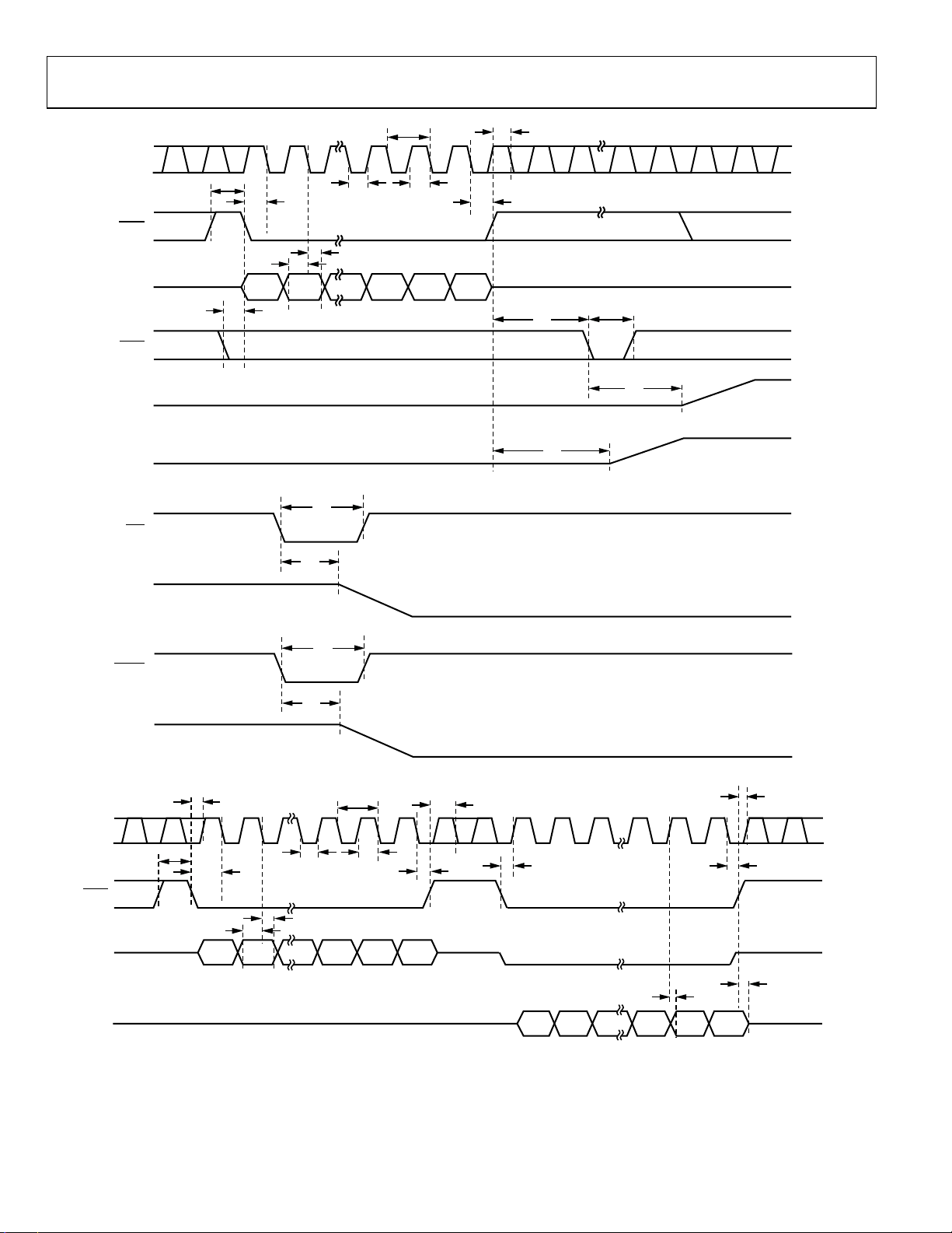
AD5780 Data Sheet
SCLK
t
t
9
t
15
SYNC
SDIN
LDAC
V
OUT
V
OUT
CLR
t
6
t
4
t
8
DB23 DB0
t
10
t
16
t
1
3
t
2
t
7
2421
t
5
t
t
11
t
14
12
t
13
SCLK
SYNC
SDIN
SDO
V
OUT
RESET
V
OUT
t
21
t
22
t
17
t
6
t
4
t
8
DB23 DB0
INPUT WORD SPECIFIES
REGISTER TO BE READ
t
3
t
9
Figure 2. Write Mode Timing Diagram
t
1
t
2
t
7
t
5
24221241
t
17
NOP CONDIT ION
DB23 DB0
t
19
09649-002
t
20
t
5
t
18
REGISTER CONTENTS CL OCKED OUT
Figure 3. Readback Mode Timing Diagram
Rev. C | Page 6 of 28
09649-003

Data Sheet AD5780
t
20
t
5
t
18
09649-004
SCLK
SYNC
SDIN
SDO
t
t
17
12 24 4825
t
6
t
4
t
8
DB23
INPUT WORD FOR DAC N
DB23
t
3
t
9
UNDEFINED
1
26
t
2
DB0 DB23 DB0
INPUT WORD FOR DAC N – 1
t
19
DB0 DB23 DB0
INPUT WORD FOR DAC N
Figure 4. Daisy-Chain Mode Timing Diagram
Rev. C | Page 7 of 28

AD5780 Data Sheet
ABSOLUTE MAXIMUM RATINGS
TA = 25°C, unless otherwise noted. Transient currents of up to
100 mA do not cause SCR latch-up.
Table 4.
Parameter Rating
VDD to AGND −0.3 V to +34 V
VSS to AGND −34 V to +0.3 V
VDD to VSS −0.3 V to +34 V
VCC to DGND −0.3 V to +7 V
IOVCC to DGND
Digital Inputs to DGND
V
to AGND −0.3 V to VDD + 0.3 V
OUT
V
to AGND −0.3 V to VDD + 0.3 V
REFP
V
to AGND VSS − 0.3 V to +0.3 V
REFN
DGND to AGND −0.3 V to +0.3 V
Operating Temperature Range, TA
Industrial −40°C to +125°C
Storage Temperature Range −65°C to +150°C
Maximum Junction Temperature,
max
T
J
Power Dissipation (TJ max − TA)/θJA
LFCSP Package
θJA Thermal Impedance 31.0°C/W
Lead Temperature JEDEC industry standard
Soldering J-STD-020
ESD (Human Body Model) 1.6 kV
−0.3 V to V
(whichever is less)
−0.3 V to IOV
+7 V (whichever is less)
150°C
+ 3 V or +7 V
CC
+ 0.3 V or
CC
Stresses above those listed under Absolute Maximum Ratings
may cause permanent damage to the device. This is a stress
rating only; functional operation of the device at these or any
other conditions above those indicated in the operational
section of this specification is not implied. Exposure to absolute
maximum rating conditions for extended periods may affect
device reliability.
This device is a high performance integrated circuit with an
ESD rating of 1.6 kV, and it is ESD sensitive. Proper precautions
must be taken for handling and assembly.
ESD CAUTION
Rev. C | Page 8 of 28

Data Sheet AD5780
PIN CONFIGURATION AND FUNCTION DESCRIPTIONS
FB
DNC
DNC
R
22
23 DNC
24 INV
21
20
GND
1
V
OUT
2
V
REFP
3
V
DD
RESET
V
DD
CLR
LDAC
NOTES
= DO NOT CONNECT. DO NOT CONNECT
1. DNC
2. NEGATIVE ANALOG
A VOLTAGE I N THE RANG
CAN BE CONNECTED. V
GND. THE PADDLE CAN BE LEFT ELECT
TO A
UNCONNECTED PRO
CONNECTION IS MADE AT THE VSS
RECOMM
CON
ENDED THAT THE PADDLE BE THERMAL
NECTED TO A COPP
THERMAL PERFORMANCE.
AD5780
4
TOP VIEW
(Not to Scale)
5
6
7
9
8
10
CC
CC
V
DNC
IOV
SUPPLY CONNECTION (V
E OF –16.5 V TO –2.5 V
SHOULD BE D
SS
VIDED THAT A S
ER PLANE FOR ENHANCED
11
SDO
Figure 5. Pin Configuration
Table 5. Pin Function Descriptions
Pin No. Mnemonic Description
1 V
2 V
3, 5 VDD Positive Analog Supply Connection. A voltage in the range of 7.5 V to 16.5 V can be connected to this pin. VDD must be
4
6
7
8 VCC Digital Supply. Voltage range is from 2.7 V to 5.5 V. VCC should be decoupled to DGND.
9 IOVCC Digital Interface Supply. Digital threshold levels are referenced to the voltage applied to this pin. Voltage range is from
10, 21,
22, 23
11 SDO Serial Data Output.
12 SDIN Serial Data Input. This device has a 24-bit input shift register. Data is clocked into the register on the falling edge of the
13 SCLK Serial Clock Input. Data is clocked into the input shift register on the falling edge of the serial clock input. Data can be
14
15 DGND Ground Reference Pin for Digital Circuitry.
16 V
17, 18 VSS Negative Analog Supply Connection. A voltage in the range of −16.5 V to −2.5 V can be connected to this pin.
19 AGND Ground Reference Pin for Analog Circuitry.
20 RFB
24 INV
EPAD VSS Negative Analog Supply Connection (VSS). A voltage in the range of −16.5 V to −2.5 V can be connected to this pin. VSS
Analog Output Voltage.
OUT
Positive Reference Voltage Input. A voltage in the range of 5 V to VDD − 2.5 V can be connected to this pin.
REFP
decoupled to AGND.
RESET
CLR
Active Low Reset. Asserting this pin returns the AD5780 to its power-on status.
Active Low Input. Asserting this pin sets the DAC register to a user defined value (see
output. The output value depends on the DAC register coding that is being used, either binary or twos complement.
LDAC
Active Low Load DAC Logic Input. This pin is used to update the DAC register and, consequently, the analog output.
When tied permanently low, the output is updated on the rising edge of
the input register is updated, but the output update is held off until the falling edge of
unconnected.
1.71 V to 5.5 V.
DNC Do Not Connect. Do not connect to these pins.
serial clock input.
transferred at rates of up to 35 MHz.
SYNC
Level Triggered Control Input (Active Low). This is the frame synchronization signal for the input data. When
low, it enables the input shift register, and data is then transferred in on the falling edges of the following clocks. The DAC
is updated on the rising edge of
Negative Reference Voltage Input.
REFN
must be decoupled to AGND.
V
SS
SYNC
.
Feedback Connection for External Amplifier. See the
Inverting Input Connection for External Amplifier. See the
must be decoupled to AGND. The paddle can be left electrically unconnected provided that a supply connection is made
at the V
pins. It is recommended that the paddle be thermally connected to a copper plane for enhanced thermal
SS
performance.
A
19
V
18
SS
V
17
SS
V
16
REFN
DGND
15
SYNC
14
SCLK
13
12
SDIN
TO THIS PIN.
).
SS
ECOUPLED
RICALLY
UPPLY
PINS. IT IS
LY
09649-005
Table 12) and updates the DAC
LDAC
SYNC
. If
is held high during the write cycle,
LDAC
AD5780 Features section for further details.
AD5780 Features section for further details.
. Do not leave the
LDAC
SYNC
pin
goes
Rev. C | Page 9 of 28
 Loading...