3.3 V Supply, Voltage Output Temperature
V
S
V
OUT
Ι
R
T
a
FEATURES
3.3 V, Single Supply Operation
Temperature Coefficient of 28 mV/°C
100°C Temperature Span (0°C to +100°C)
Accuracy Better Than 2.5% of Full Scale
Linearity Better Than 0.5% of Full Scale
Output Proportional to Temperature × V
Minimal Self-Heating
High Level, Low Impedance Output
Reverse Supply Protected
APPLICATIONS
Microprocessor Thermal Management
Battery and Low Powered Systems
Power Supply Temperature Monitoring
System Temperature Compensation
Board Level Temperature Sensing
MARKETS
Computers
Portable Electronic Equipment
Industrial Process Control
Instrumentation
Sensor with Signal Conditioning
AD22103*
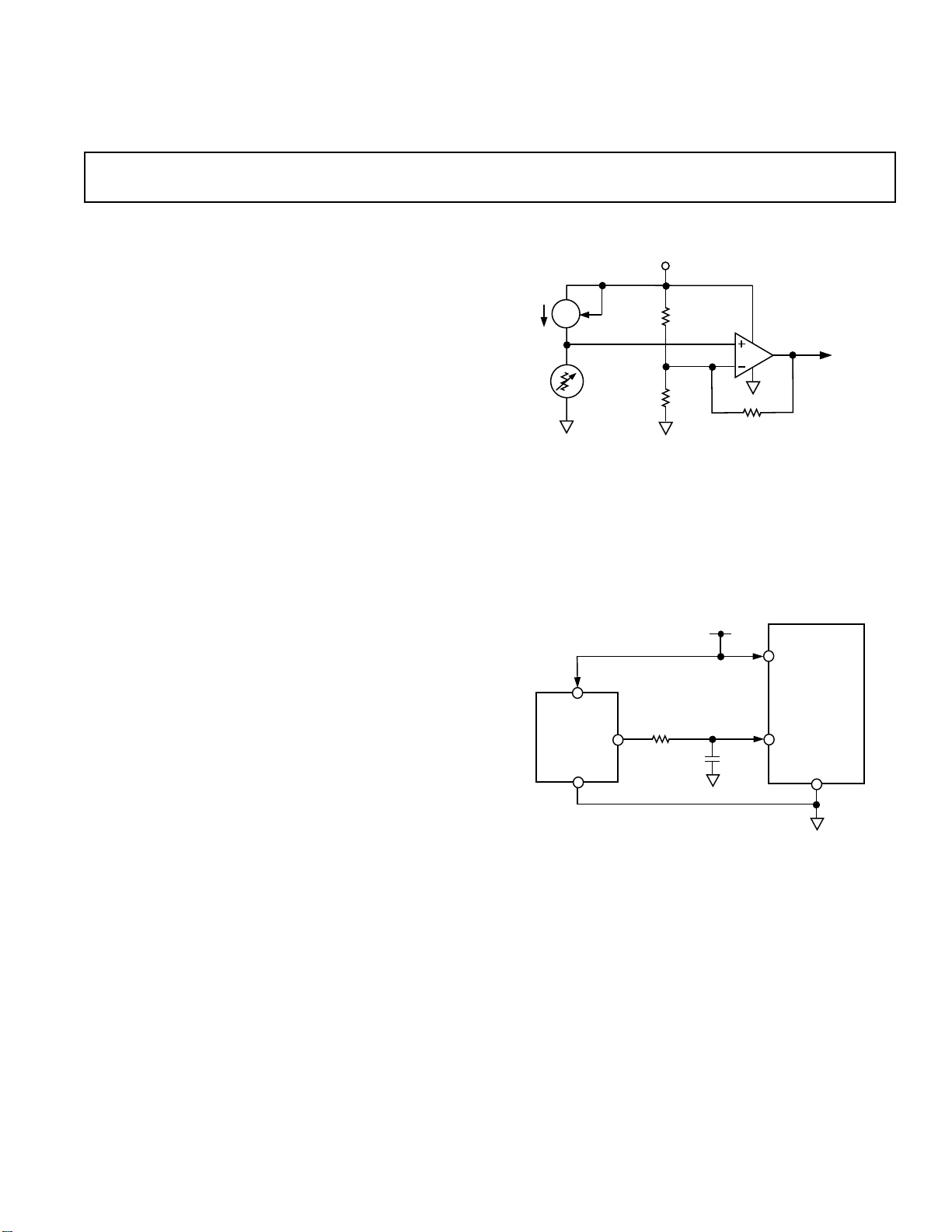
SIMPLIFIED BLOCK DIAGRAM
S
GENERAL DESCRIPTION
The AD22103 is a monolithic temperature sensor with on-chip
signal conditioning. It can be operated over the temperature
range 0°C to +100°C, making it ideal for use in numerous 3.3 V
applications.
The signal conditioning eliminates the need for any trimming,
buffering or linearization circuitry, greatly simplifying the system
design and reducing the overall system cost.
The output voltage is proportional to the temperature times the
supply voltage (ratiometric). The output swings from 0.25 V at
0°C to +3.05 V at +100°C using a single +3.3 V supply.
Due to its ratiometric nature, the AD22103 offers a cost effective solution when interfacing to an analog-to-digital converter.
This is accomplished by using the ADC’s power supply as a reference to both the ADC and the AD22103 (See Figure 1),
eliminating the need for and cost of a precision reference.
Protected by U.S. Patent Nos. 5030849 and 5243319
*
.
AD22103
+3.3V
REFERENCE
SIGNAL OUTPUT
DIRECT TO ADC
V
O
1kΩ
0.1µF
INPUT
Figure 1. Application Circuit
ANALOG TO
DIGITAL
CONVERTER
Information furnished by Analog Devices is believed to be accurate and
reliable. However, no responsibility is assumed by Analog Devices for its
use, nor for any infringements of patents or other rights of third parties
which may result from its use. No license is granted by implication or
otherwise under any patent or patent rights of Analog Devices.
© Analog Devices, Inc., 1995
One Technology Way, P.O. Box 9106, Norwood. MA 02062-9106, U.S.A.
Tel: 617/329-4700 Fax: 617/326-8703
REV. 0

AD22103–SPECIFICATIONS
(TA = +25°C and VS = +2.7 V to +3.6 V unless otherwise noted)
AD22103K
Parameter Min Typ Max Units
TRANSFER FUNCTION V
TEMPERATURE COEFFICIENT (V
OUT
= (V
/3.3 V) × [0.25 V + (28 mV/°C) × T
S
/3.3 V) × 28 mV/°C
S
]V
A
TOTAL ERROR
Initial Error
= +25°C ±0.5 ±2.0 °C
T
A
Error over Temperature
T
A = TMIN
Nonlinearity
TA = T
to T
MAX
MIN to TMAX
±0.75 ±2.5 °C
0.1 0.5 % FS
1
OUTPUT CHARACTERISTICS
Nominal Output Voltage
V
= 3.3 V, T
S
V
= 3.3 V, T
S
VS = 3.3 V, T
= 0°C 0.25 V
A
= +25°C 0.95 V
A
= +100°C 3.05 V
A
POWER SUPPLY
Operating Voltage +2.7 +3.3 +3.6 V
Quiescent Current 350 500 600 µA
TEMPERATURE RANGE
Guaranteed Temperature Range 0 +100 °C
Operating Temperature Range 0 +100 °C
PACKAGE TO-92
SOIC
NOTES
1
FS (Full Scale) is defined as that of the operating temperature range, 0°C to +100°C. The listed max specification limit applies to the guaranteed temperature range.
For example, the AD22103K has a nonlinearity of (0.5%) × (100°C) = 0.5°C over the guaranteed temperature range of 0°C to +100°C.
Specifications subject to change without notice.
CHIP SPECIFICATIONS
(TA = +25°C and VS = +3.3 V unless otherwise noted)
Parameter Min Typ Max Units
TRANSFER FUNCTION V
TEMPERATURE COEFFICIENT (V
OUT
= (V
/3.3 V) × [0.25 V + (28 mV/°C) × T
S
/3.3 V) × 28 mV/°C
S
]V
A
OUTPUT CHARACTERISTICS
Error
= +25°C ±0.5 Note 1 °C
T
A
Nominal Output Voltage
T
= +25°C 0.95 V
A
POWER SUPPLY
Operating Voltage +2.7 +3.3 +3.6 V
Quiescent Current 350 500 600 µA
TEMPERATURE RANGE
Guaranteed Temperature Range 25 °C
Operating Temperature Range 0 +100 °C
NOTES
1
Max specs cannot be guaranteed on chips, however, performance once assembled should be commensurate with the specifications listed in the top table.
Specifications subject to change without notice.
–2–
REV. 0
 Loading...