Stereo, Single-Supply
a
FEATURES
Complete, Low Cost Stereo DAC System in a Single Die
Package
Variable Rate Oversampling Interpolation Filter
Multibit SD Modulator with Triangular PDF Dither
Discrete and Continuous Time Analog Reconstruction
Filters
Extremely Low Out-of-Band Energy
64 Step (1 dB/Step) Analog Attenuator with Mute
Buffered Outputs with 2 kV Output Load Drive
Rejects Sample Clock Jitter
94 dB Dynamic Range, –88 dB THD+N Performance
Option for Analog De-emphasis Processing with
External Passive Components
60.18 Maximum Phase Linearity Deviation
Continuously Variable Sample Rate Support
Digital Phase Locked Loop Based Asynchronous Master
Clock
On-Chip Master Clock Oscillator, Only External Crystal
Is Required
Power-Down Mode
Flexible Serial Data Port (I
Right-Justified and DSP Serial Port Modes)
SPI* Compatible Serial Control Port
Single +5 V Supply
28-Pin SOIC and SSOP Packages
APPLICATIONS
Digital Cable TV and Direct Broadcast Satellite Set-Top
Decoder Boxes
Digital Video Disc, Video CD and CD-I Players
High Definition Televisions, Digital Audio Broadcast
Receivers
CD, CD-R, DAT, DCC, ATAPI CD-ROM and MD Players
Digital Audio Workstations, Computer Multimedia
Products
16- OR 18-BIT
DIGITAL DATA
2
S-Justified, Left-Justified,
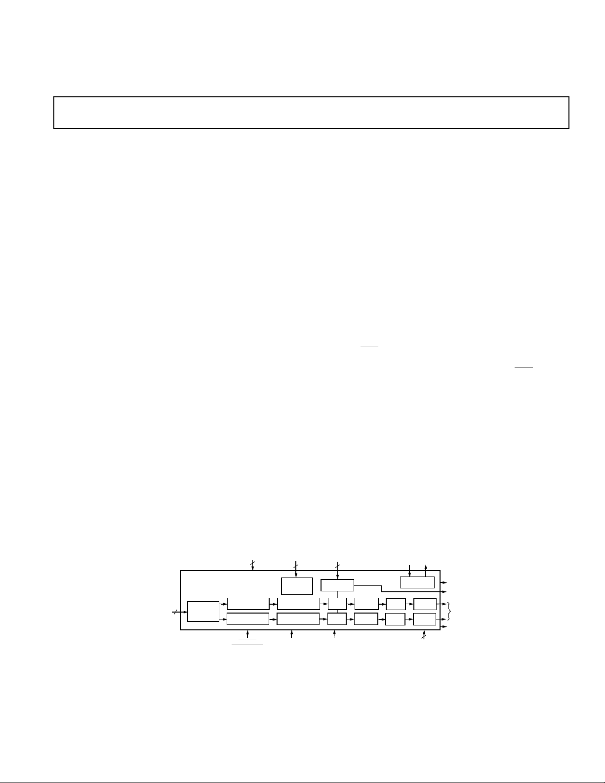
FUNCTIONAL BLOCK DIAGRAM
AD1859
VARIABLE RATE
INTERPOLATION
VARIABLE RATE
INTERPOLATION
POWER
DOWN/RESET
INPUT
6
SERIAL
DATA
INTERFACE
DIGITAL
SUPPLY
2
∑∆ MODULATOR
∑∆ MODULATOR
CONTROL
DATA
INPUT
3
SERIAL
CONTROL
INTERFACE
MULTIBIT
MULTIBIT
MUTE
18-Bit Integrated SD DAC
AD1859
PRODUCT OVERVIEW
The AD1859 is a complete 16-/18-bit single-chip stereo digital
audio playback subsystem. It comprises a variable rate
interpolation filter, a revolutionary multibit sigma-delta (∑∆)
modulator with dither, a jitter-tolerant DAC, switched capacitor
and continuous time analog filters, and analog output drive circuitry. Other features include an on-chip stereo attenuator and
mute, programmed through an SPI-compatible serial control
port.
The key differentiating feature of the AD1859 is its asynchronous master clock capability. Previous ∑∆ audio DACs required a high frequency master clock at 256 or 384 times the
intended audio sample rate. The generation and management
of this high frequency synchronous clock is burdensome to the
board level designer. The analog performance of conventional
single bit ∑∆ DACs is also dependent on the spectral purity of
the sample and master clocks. The AD1859 has a digital Phase
Locked Loop (PLL) which allows the master clock to be asynchronous, and which also strongly rejects jitter on the sample
clock (left/
right clock). The digital PLL allows the AD1859 to
be clocked with a single frequency (27 MHz for example) while
the sample frequency (as determined from the left/
can vary over a wide range. The digital PLL will lock to the
new sample rate in approximately 100 ms. Jitter components
15 Hz above and below the sample frequency are rejected by
6 dB per octave. This level of jitter rejection is unprecedented
in audio DACs.
The AD1859 supports continuously variable sample rates with
essentially linear phase response, and with an option for external
analog de-emphasis processing. The clock circuit includes an
on-chip oscillator, so that the user need only provide an external
crystal. The oscillator may be overdriven, if desired, with an external clock source.
(continued on page 7)
REFERENCE
FILTER AND
GROUND
2
VOLTAGE
REFERENCE
DAC
DAC
DE-EMPHASIS
ANALOG
FILTER
ANALOG
FILTER
ASYNCHRONOUS
CLOCK/CRYSTAL
DPLL/CLOCK
MANAGER
ATTEN/
MUTE
ATTEN/
MUTE
OUTPUT
BUFFER
OUTPUT
BUFFER
ANALOG
SUPPLY
2
DE-EMPHASIS
SWITCH LEFT
COMMON MODE
ANALOG
OUTPUTS
DE-EMPHASIS
SWITCH RIGHT
digital
right clock)
*SPI is a registered trademark of Motorola, Inc.
REV. A
Information furnished by Analog Devices is believed to be accurate and
reliable. However, no responsibility is assumed by Analog Devices for its
use, nor for any infringements of patents or other rights of third parties
which may result from its use. No license is granted by implication or
otherwise under any patent or patent rights of Analog Devices.
© Analog Devices, Inc., 1996
One Technology Way, P.O. Box 9106, Norwood. MA 02062-9106, U.S.A.
Tel: 617/329-4700 Fax: 617/326-8703

AD1859–SPECIFICA TIONS
TEST CONDITIONS UNLESS OTHERWISE NOTED
Supply Voltages (AVDD, DVDD) +5.0 V
Ambient Temperature 25 °C
Input Clock (F
Input Signal 1001.2938 Hz
Input Sample Rate 44.1 kHz
Measurement Bandwidth 10 Hz to 20 kHz
Input Data Word Width 18 Bits
Load Capacitance 100 pF
Input Voltage HI (V
Input Voltage LO (V
NOTES
I2S-Justified Mode (Ref. Figure 3).
Device Under Test (DUT) is bypassed, decoupled and dc-coupled as shown in Figure 17 (no de-emphasis circuit).
Performance of the right and left channels are identical (exclusive of “Interchannel Gain Mismatch” and “Interchannel Phase Deviation” specifications).
Attenuation setting is 0 dB.
Values in bold typeface are tested; all others are guaranteed, not tested.
ANALOG PERFORMANCE
Resolution 18 Bits
Dynamic Range (20 to 20 kHz, –60 dB Input)
(No A-Weight Filter) 85.7 91 dB
(With A-Weight Filter) 88 94 dB
Total Harmonic Distortion + Noise –88 –84 dB
Analog Outputs
Single-Ended Output Range (± Full Scale) 2.8 3.0 3.2 V p-p
Output Impedance at Each Output Pin 17 24 Ω
Output Capacitance at Each Output Pin 20 pF
External Load Impedance (THD +N ≤ –84 dB) 750 2K Ω
Out-of-Band Energy (0.5 × F
CMOUT 2.05 2.25 2.45 V
DC Accuracy
Gain Error ±1 65 %
Interchannel Gain Mismatch 0.01 0.225 dB
Gain Drift 140 270 ppm/°C
Interchannel Crosstalk (EIAJ Method) 101 dB
Interchannel Phase Deviation ±0.1 Degrees
Attenuator Step Size 0.6 1.0 1.4 dB
Attenuator Range Span –61.5 –62.5 –63.5 dB
Mute Attenuation –70 –74.2 dB
De-Emphasis Switch (EMPL, EMPR) DC Resistance 3 10 50 Ω
) 27.1656 MHz
MCLK
–0.5 dB Full Scale
) 2.4 V
IH
) 0.8 V
IL
to 100 kHz) –72.5 dB
S
Min Typ Max Units
0.004 0.0063 %
DIGITAL INPUTS
Min Typ Max Units
Input Voltage HI (V
Input Voltage LO (V
Input Leakage (I
Input Leakage (I
) 2.4 V
IH
) 0.8 V
IL
@ VIH = 2.4 V) 1 6 µA
IH
@ VIL = 0.8 V) 1 6 µA
IL
Input Capacitance 20 pF
–2–
REV. A

DIGITAL TIMING (Guaranteed over –40°C to +105°C, AVDD = DVDD = +5.0 V ± 10%)
Min Typ Max Units
t
DBH
t
DBL
t
DBP
t
DLS
t
DLH
t
DDS
t
DDH
t
CCH
t
CCL
t
CCP
t
CSU
t
CHD
t
CLD
t
CLL
t
CLH
t
PDRP
BCLK HI Pulse Width 25 ns
BCLK LO Pulse Width 25 ns
BCLK Period 50 ns
LRCLK Setup 5 ns
LRCLK Hold (DSP Serial Port Style Mode Only) 0 ns
SDATA Setup 0 ns
SDATA Hold 5 ns
CCLK HI Pulse Width 15 ns
CCLK LO Pulse Width 15 ns
CCLK Period 30 ns
CDATA Setup 0 ns
CDATA Hold 5 ns
CLATCH Delay 15 ns
CLATCH LO Pulse Width 5 ns
CLATCH HI Pulse Width 10 ns
PD/RST LO Pulse Width 4 MCLK Periods
(≈150 ns @ 27 MHz)
t
MCP
F
MC
t
MCH
t
MCL
MCLK Period 30 37 60 ns
MCLK Frequency (1/t
) 17 27 33 MHz
MCP
MCLK HI Pulse Width 15 ns
MCLK LO Pulse Width 15 ns
AD1859
POWER
Min Typ Max Units
Supplies
Voltage, Analog and Digital 4.5 5 5.5 V
Analog Current 29.5 36 mA
Analog Current—Power Down 0.5 15 µA
Digital Current 23.5 30 mA
Digital Current—Power Down 6 9.5 mA
Dissipation
Operation—Both Supplies 265 330 mW
Operation—Analog Supply 147.5 180 mW
Operation—Digital Supply 117.5 150 mW
Power Down—Both Supplies 30 48 mW
Power Supply Rejection Ratio
1 kHz 300 mV p-p Signal at Analog Supply Pins 55 dB
20 kHz 300 mV p-p Signal at Analog Supply Pins 52 dB
TEMPERATURE RANGE
Min Typ Max Units
Specifications Guaranteed 25 °C
Functionality Guaranteed –40 +105 °C
Storage –55 +125 °C
PACKAGE CHARACTERISTICS
Typ Units
SOIC θ
SOIC θ
SSOP θ
(Thermal Resistance [Junction-to-Ambient]) 120.67 °C/W
JA
(Thermal Resistance [Junction-to-Case]) 13.29 °C/W
JC
(Thermal Resistance [Junction-to-Ambient]) 190.87 °C/W
JA
SSOP θJC (Thermal Resistance [Junction-to-Case]) 15.52 °C/W
REV. A
–3–

AD1859
WARNING!
ESD SENSITIVE DEVICE
NC = NO CONNECT
CMOUT
DEEMP
FILT
FGND
NC
EMPL
OUTL
AGND
MUTE
NC
AV
DD
NC
EMPR
OUTR
18/16
CLATCH
IDPM0 CDATA
IDPM1
CCLK
DGND
SDATA
DV
DD
LRCLK
XTALI/MCLK
BCLK XTALO
13
18
1
2
28
27
5
6
7
24
23
22
3
4
26
25
821
920
10
19
11
12 17
16
14
15
TOP VIEW
(Not to Scale)
AD1859
PD/RST
ABSOLUTE MAXIMUM RATINGS*
Min Typ Max Units
to DGND –0.3 6 V
DV
DD
to AGND –0.3 6 V
AV
DD
Digital Inputs DGND – 0.3 DV
Analog Inputs AGND – 0.3 AV
AGND to DGND –0.3 0.3 V
Reference Voltage Indefinite Short Circuit to Ground
Soldering +300 °C
*Stresses greater than those listed under “Absolute Maximum Ratings” may cause permanent damage to the device. This is a stress rating only and functional operation
of the device at these or any other conditions above those indicated in the operational section of this specification is not implied. Exposure to absolute maximum rating
conditions for extended periods may affect device reliability.
DIGITAL FILTER CHARACTERISTICS
Min Typ Max Units
Passband Ripple ±0.045 dB
Stopband
48 kHz F
1
Attenuation 62 dB
S
Passband 0 21.312 kHz
Stopband 26.688 6117 kHz
44.1 kHz F
S
Passband 0 19.580 kHz
Stopband 24.520 5620 kHz
32 kHz F
S
Passband 0 14.208 kHz
Stopband 17.792 4078 kHz
Other F
S
Passband 0 0.444 F
Stopband 0.556 127.444 F
Group Delay 40/F
Group Delay Variation 0 µs
+ 0.3 V
DD
+ 0.3 V
DD
10 sec
S
sec
S
S
ANALOG FILTER CHARACTERISTICS
Passband Ripple –0.075 dB
Stopband Attenuation (at 64 × FS)58 dB
NOTE
1
Stopband nominally repeats itself at multiples of 128 × FS, where FS is the input word rate. Thus the digital filter will attenuate to 62 dB across the frequency
spectrum except for a range ±0.55 × FS wide at multiples of 128 × FS.
Model Range Description Option
AD1859JR –40°C to +105°C 28-Lead SOIC R-28
AD1859JRS –40°C to +105°C 28-Lead SSOP RS-28
CAUTION
ESD (electrostatic discharge) sensitive device. Electrostatic charges as high as 4000 V readily
accumulate on the human body and test equipment and can discharge without detection.
Although the AD1859 features proprietary ESD protection circuitry, permanent damage may
occur on devices subjected to high energy electrostatic discharges. Therefore, proper ESD
precautions are recommended to avoid performance degradation or loss of functionality.
ORDERING GUIDE
Temperature Package Package
–4–
Min Typ Max Units
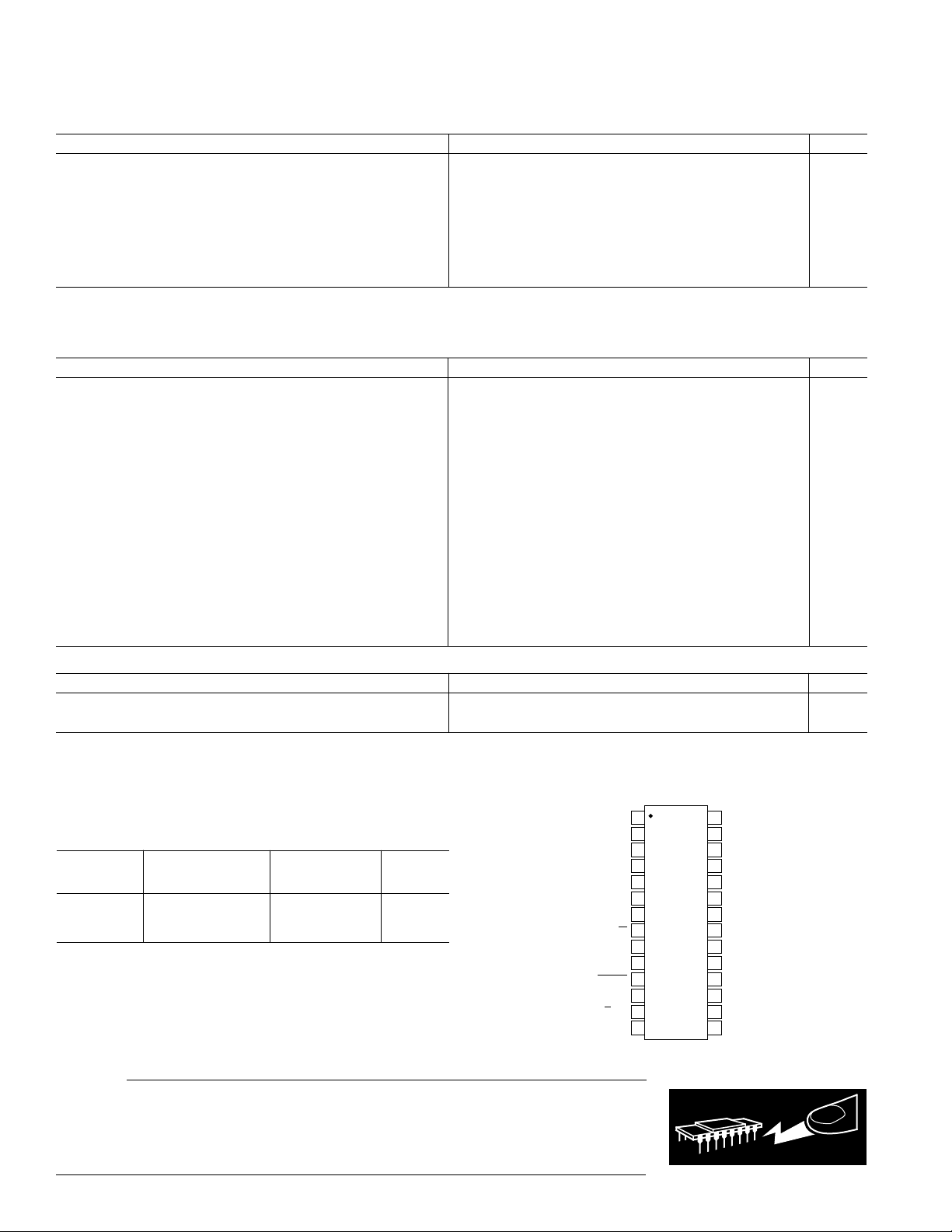
PIN CONNECTIONS
REV. A

AD1859
DEFINITIONS
Dynamic Range
The ratio of a full-scale output signal to the integrated output
noise in the passband (0 to 20 kHz), expressed in decibels (dB).
Dynamic range is measured with a –60 dB input signal and is
equal to (S/[THD+N]) + 60 dB. Note that spurious harmonics
are below the noise with a –60 dB input, so the noise level establishes the dynamic range. This measurement technique is
consistent with the recommendations of the Audio Engineering
Society (AES17-1991) and the Electronics Industries Association
of Japan (EIAJ CP-307).
Total Harmonic Distortion + Noise (THD+N)
The ratio of the root-mean-square (rms) value of a full-scale
fundamental input signal to the rms sum of all other spectral
components in the passband, expressed in decibels (dB) and
percentage.
Passband
The region of the frequency spectrum unaffected by the attenuation of the digital interpolation filter.
Passband Ripple
The peak-to-peak variation in amplitude response from equalamplitude input signal frequencies within the passband, expressed in decibels.
Stopband
The region of the frequency spectrum attenuated by the digital interpolation filter to the degree specified by “stopband
attenuation.”
Gain Error
With a near full-scale input, the ratio of actual output to expected output, expressed as a percentage.
Interchannel Gain Mismatch
With identical near full-scale inputs, the ratio of outputs of the
two stereo channels, expressed in decibels.
Gain Drift
Change in response to a near full-scale input with a change in
temperature, expressed as parts-per-million (ppm) per °C.
Crosstalk (EIAJ method)
Ratio of response on one channel with a zero input to a full-scale
1 kHz sine-wave input on the other channel, expressed in decibels.
Interchannel Phase Deviation
Difference in output sampling times between stereo channels,
expressed as a phase difference in degrees between 1 kHz inputs.
Power Supply Rejection
With zero input, signal present at the output when a 300 mV
p-p signal is applied to power supply pins, expressed in decibels
of full scale.
Group Delay
Intuitively, the time interval required for an input pulse to appear at the converter’s output, expressed in seconds (s). More
precisely, the derivative of radian phase with respect to radian
frequency at a given frequency.
Group Delay Variation
The difference in group delays at different input frequencies.
Specified as the difference between the largest and the smallest
group delays in the passband, expressed in microseconds (µs).
PIN DESCRIPTIONS
Digital Audio Serial Input Interface
Pin Name Number I/O Description
SDATA 12 I Serial input, MSB first, contain-
ing two channels of 16 or 18 bits
of twos complement data per
channel.
BCLK 14 I Bit clock input for input data.
Need not run continuously; may
be gated or used in a burst
fashion.
L
RCLK 13 I Left/right clock input for input
data. Must run continuously.
IDPM0 9 I Input serial data port mode
control zero. With IDPM1,
defines one of four serial input
modes.
IDPM1 10 I Input serial data port mode con-
trol one. With IDPM0, defines
one of four serial input modes.
18/
16 8 I 18-bit or 16-bit input data mode
control. Connect this signal HI
for 18-bit input mode, LO for
16-bit input mode.
Serial Control Port Interface
Pin Name Number I/O Description
CDATA 20 I Serial control input, MSB first,
containing 8 bits of unsigned
data per channel. Used for
specifying channel specific
attenuation and mute.
CCLK 19 I Control clock input for control
data. Control input data must
be valid on the rising edge of
CCLK. CCLK may be continuous or gated.
CLATCH 21 I Latch input for control data. This
input is rising edge sensitive.
REV. A
–5–
 Loading...