Analog Devices AD1858JRSRL, AD1858JRS, AD1857JRSRL, AD1857JRS Datasheet

Stereo, Single Supply
a
16-, 18- and 20-Bit Sigma-Delta DACs
FEATURES
Low Cost, High Performance Stereo DACs
128 Times Oversampling Interpolation Filter
Multibit SD Modulator with Triangular PDF Dither
Discrete Time and Continuous Time Analog
Reconstruction Filters
Extremely Low Out-of-Band Energy
Buffered Outputs with 2 kV Output Load Drive
94 dB Dynamic Range, –90 dB THD+N Performance
Digital De-emphasis and Mute
60.18C Maximum Phase Linearity Deviation
Continuously Variable Sample Rate Support
Power-Down Mode
16-, 18- and 20-Bit I
2
S-Justified, Left-Justified Modes
Offered on AD1857
Accepts 24-Bit Word
16-Bit Right-Justified and DSP Serial Port Modes
Offered on AD1858
Single +5 V Supply
20-Pin SSOP Package
APPLICATIONS
Digital Cable TV and Direct Broadcast Satellite Set-Top
Decoder Boxes
Video Laser Disk, Video CD and CD-I Players
High Definition Televisions, Digital Audio Broadcast
Receivers
CD, CD-R, DAT, DCC and MD Players
Digital Audio Workstations, Computer Multimedia
Products
AD1857/AD1858
PRODUCT OVERVIEW
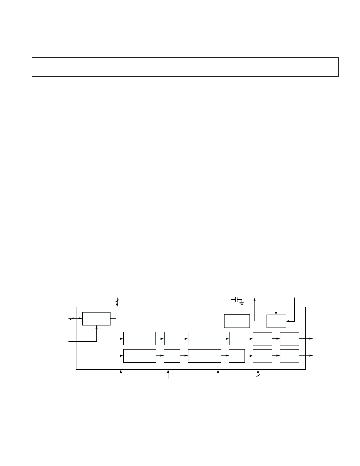
The AD1857/AD1858 are complete single-chip stereo digital
audio playback components. They each comprise an advanced
digital interpolation filter, a revolutionary “linearity-compensated”
multibit sigma-delta (∑∆) modulator with dither, a jitter-tolerant
DAC, switched capacitor and continuous time analog filters and
analog output drive circuitry. Other features include digital
de-emphasis processing and mute. The AD1857/AD1858
support continuously variable sample rates with essentially
linear phase response, and support 50/15 µs digital de-emphasis
intended for “Redbook” 44.1 kHz sample frequency playback
from Compact Discs. The user must provide a master clock that
is synchronous with the left/right clock at 256 or 384 times the
intended sample frequency.
The AD1857/AD1858 have a simple but very flexible serial data
input port that allows for glueless interconnection to a variety of
ADCs, DSP chips, AES/EBU receivers and sample rate converters. The AD1857 serial data input port can be configured
in either 16-bit, 18-bit or 20-bit left-justified or I
modes. The AD1858 serial data input port can be configured in
either 16-bit right-justified or DSP serial port compatible modes.
The AD1857/AD1858 accept serial audio data in MSB first,
twos-complement format. A power-down mode is offered to
minimize power consumption when the device is inactive. The
AD1857/AD1858 operate from a single +5V power supply.
They are fabricated on a single monolithic integrated circuit and
housed in 20-pin SSOP packages for operation over the
temperature range 0°C to +70°C.
2
S-justified
FUNCTIONAL BLOCK DIAGRAM
DIGITAL
SUPPLY
2
16-/18-/20-BIT
DATA INPUT
DIGITAL
SERIAL
MODE
3
SERIAL DATA
INTERFACE
INTERPOLATION
INTERPOLATION
DE-EMPHASIS
128x
FILTER
128x
FILTER
AD1857/AD1858
MUTE
MUTE
MUTE
REV. 0
Information furnished by Analog Devices is believed to be accurate and
reliable. However, no responsibility is assumed by Analog Devices for its
use, nor for any infringements of patents or other rights of third parties
which may result from its use. No license is granted by implication or
otherwise under any patent or patent rights of Analog Devices.
MODE
CLOCK
OUTPUT
BUFFER
OUTPUT
BUFFER
IN
ANALOG
OUTPUTS
ANALOG
FILTER
ANALOG
FILTER
4
CLOCK
CLOCK
CIRCUIT
COMMON
MODE
VOLTAGE
REFERENCE
MULTIBIT
Σ∆ MODULATOR
MULTIBIT
Σ∆ MODULATOR
POWER-DOWN/RESET
One Technology Way, P.O. Box 9106, Norwood, MA 02062-9106, U.S.A.
Tel: 617/329-4700 World Wide Web Site: http://www.analog.com
Fax: 617/326-8703 © Analog Devices, Inc., 1997
DAC
DAC
ANALOG
SUPPLY

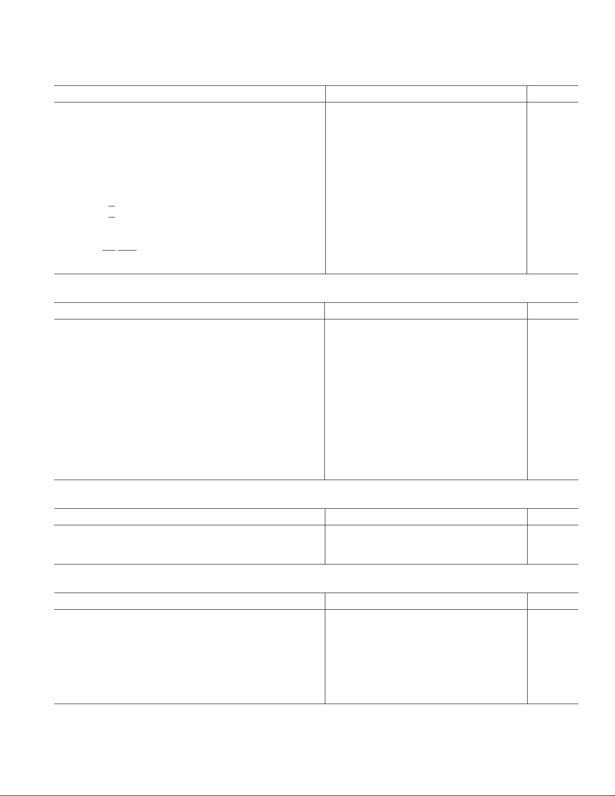
AD1857/AD1858–SPECIFICA TIONS
TEST CONDITIONS UNLESS OTHERWISE NOTED
Supply Voltages (AVDD, DVDD) +5.0 V
Ambient Temperature 25°C
Input Clock (F
Input Signal 1.0013 kHz
Input Sample Rate 44.1 kHz
Measurement Bandwidth 20 Hz to 20 kHz
AD1857 Input Data Wordwidth 18 Bits
AD1858 Input Data Wordwidth 16 Bits
Load Capacitance 100 pF
Load Impedance 47 kΩ
Input Voltage HI (V
Input Voltage LO (V
I2S-Justified Mode (Ref. Figure 7) for AD1857, Right-Justified Mode (Ref. Figure 8) for AD1858.
Performance of the right and left channels are identical (exclusive of the Interchannel Gain Mismatch and Interchannel Phase Deviation specifications).
Values in bold typeface are tested, all others are guaranteed, not tested.
ANALOG PERFORMANCE
AD1857 Resolution 18 Bits
AD1858 Resolution 16 Bits
Dynamic Range (20 Hz to 20 kHz, –60 dB Input)
No A-Weight Filter 91 dB
With A-Weight Filter 94 dB
Total Harmonic Distortion + Noise –90 –85 dB
Analog Outputs
Single-Ended Output Range (± Full Scale) 2.8 3.0 3.2 V p-p
Output Impedance at Each Output Pin <200 Ω
Output Capacitance at Each Output Pin 20 pF
Out-of-Band Energy (0.5 × F
CMOUT 2.1 2.25 2.4 V
DC Accuracy
Gain Error ±3.0 67.5 %
Interchannel Gain Mismatch 0.01 60.2 dB
Gain Drift 150 300 ppm/°C
Interchannel Crosstalk (EIAJ method) –120 –100 dB
Interchannel Phase Deviation ±0.1 Degrees
Mute Attenuation –100 –90 dB
De-emphasis Gain Error ±0.1 dB
) 11.2896 MHz (256 × FS Mode)
MCLK
–0.5 dB Full Scale
) 2.4 V
IH
) 0.8 V
IL
to 100 kHz) –72.5 dB
S
Min Typ Max Units
0.003 0.006 %
DIGITAL I/O
Min Max Units
Input Voltage HI (VIH) 2.4 V
Input Voltage LO (V
Input Leakage (I
Input Leakage (I
) 0.8 V
IL
@ VIH = 2.4 V) 10 µA
IH
@ V
IL
= 0.8 V) 10 µA
IL
Input Capacitance 20 pF
–2–
REV. 0

DIGITAL TIMING (Guaranteed over 0°C to +70°C, AVDD = DVDD = +5.0 V ± 5%)
Min Max Units
AD1857/AD1858
t
DML
t
DMH
t
DMP
t
DML
t
DMH
t
DMP
t
DBH
t
DBL
t
DBP
t
DLS
t
DLH
t
DDS
t
DDH
t
PDRP
MCLK LO Pulse Width (256 × FS Mode) 35 ns
MCLK HI Pulse Width (256 × FS Mode) 40 ns
MCLK Period (256 × FS Mode) 88.577 ns
MCLK LO Pulse Width (384 × FS Mode) 25 ns
MCLK HI Pulse Width (384 × FS Mode) 25 ns
MCLK Period (384 × FS Mode) 59.0514 ns
BCLK HI Pulse Width 20 ns
BCLK LO Pulse Width 20 ns
BCLK Period 354.308 ns
LRCLK Setup 20 ns
LRCLK Hold 5 ns
SDATA Setup 5 ns
SDATA Hold 10 ns
PD/RST LO Pulse Width 4 MCLK Periods ns
(355 ns @ 11.2896 MHz)
POWER
Min Typ Max Units
Supplies
Voltage, Analog and Digital 4.75 5 5.25 V
Analog Current 35 40 mA
Analog Current – Power-Down 30 60 µA
Digital Current 20 25 mA
Digital Current – Power-Down 5 11 mA
Dissipation
Operation – Both Supplies 275 325 mW
Operation – Analog Supply 175 200 mW
Operation – Digital Supply 100 125 mW
Power-Down – Both Supplies 25 56 mW
Power Supply Rejection Ratio
1 kHz 300 mV p-p Signal at Analog Supply Pins –60 dB
20 kHz 300 mV p-p Signal at Analog Supply Pins –50 dB
TEMPERATURE RANGE
Min Typ Max Units
Specifications Guaranteed 25 °C
Functionality Guaranteed 0 70 °C
Storage –55 125 °C
ABSOLUTE MAXIMUM RATINGS*
Min Typ Max Units
DVDD to DGND –0.3 6 V
AV
to AGND –0.3 6 V
DD
Digital Inputs DGND – 0.3 DV
Analog Outputs AGND – 0.3 AV
+ 0.3 V
DD
+ 0.3 V
DD
AGND to DGND –0.3 0.3 V
Reference Voltage Indefinite Short Circuit to Ground
Soldering +300 °C
10 sec
*Stresses greater than those listed under Absolute Maximum Ratings may cause permanent damage to the device. This is a stress rating only; functional operation of the
device at these or any other conditions above those indicated in the operational section of this specification is not implied. Exposure to absolute maximum rating conditions
for extended periods may affect device reliability.
REV. 0
–3–

AD1857/AD1858
WARNING!
ESD SENSITIVE DEVICE
PACKAGE CHARACTERISTICS
Min Typ Max Units
θJA (Thermal Resistance [Junction-to-Ambient]) 195 °C/W
θJC (Thermal Resistance [Junction-to-Case]) 13 °C/W
DIGITAL FILTER CHARACTERISTICS
Min Max Units
Passband Ripple ±0.045 dB
Stopband
48 kHz F
1
Attenuation 62 dB
S
Passband 0 21.312 kHz
Stopband 26.688 6117 kHz
44.1 kHz F
S
Passband 0 19.580 kHz
Stopband 24.520 5620 kHz
32 kHz F
S
Passband 0 14.208 kHz
Stopband 17.792 4078 kHz
Other F
Group Delay 40/F
S
Passband 0 0.444 F
Stopband 0.556 127.444 F
S
S
S
sec
Group Delay Variation 0 µs
ANALOG FILTER CHARACTERISTICS
Min Typ Max Units
Passband Ripple –0.075 dB
Stopband Attenuation (at 64 × FS)58dB
NOTES
1
Stopband nominally repeats itself at multiples of 128 × FS, where FS is the input word rate. Thus the digital filter will attenuate to 62 dB across the frequency
spectrum, except for a range ±0.55 × FS wide at multiples of 128 × FS.
Specifications subject to change without notice.
ORDERING GUIDE
Package Package
Model Temperature Description Option*
AD1857JRS 0°C to +70°C 20-Lead SSOP RS-20
AD1857JRSRL 0°C to +70°C 20-Lead SSOP RS-20 on
13" Reels
AD1858JRS 0°C to +70°C 20-Lead SSOP RS-20
AD1858JRSRL 0°C to +70°C 20-Lead SSOP RS-20 on
13" Reels
*RS = Shrink Small Outline
CAUTION
ESD (electrostatic discharge) sensitive device. Electrostatic charges as high as 4000 V readily
accumulate on the human body and test equipment and can discharge without detection. Although
the AD1857/AD1858 feature proprietary ESD protection circuitry, permanent damage may occur on
devices subjected to high energy electrostatic discharges. Therefore, proper ESD precautions are
recommended to avoid performance degradation or loss of functionality.
–4–
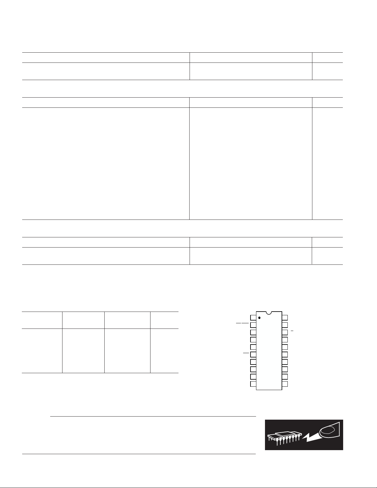
PIN CONFIGURATION
MCLK
PD/RST
MODE
NC
DEEMP
256
384/
AV
OUTL
AGND
CMOUT
DD
1
2
3
4
AD1857
5
AD1858
TOP VIEW
6
(Not to Scale)
7
8
9
10
NC = NO CONNECT
20
19
18
17
16
15
14
13
12
11
SDATA
BCLK
LRCLK
DV
DD
DGND
MUTE
AV
DD
OUTR
AGND
FILT
REV. 0

AD1857/AD1858
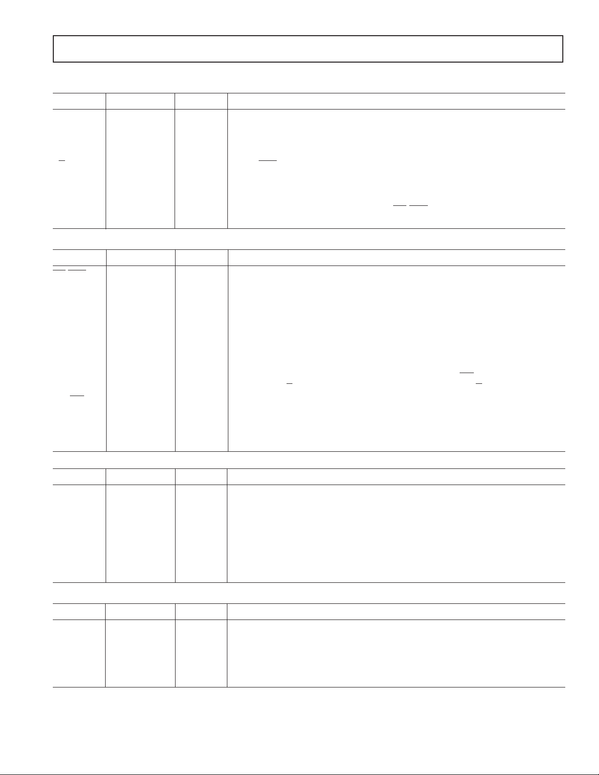
PIN LIST
Digital Audio Serial Input Interfaces
Pin Name Number I/O Description
SDATA 20 I Serial input, MSB first, containing two channels of 16, 18 or 20bits (AD1857) or
16 bits (AD1858) of twos complement data per channel.
BCLK 19 I Bit clock input for input data. Need not run continuously; may be gated or used in a
burst fashion.
L
RCLK 18 I Left/right clock input for input data. Must run continuously.
MODE 3 I Input serial data port mode control. Selects between I
(LO) on the AD1857. Selects between DSP serial port style mode (HI) and rightjustified (LO) on the AD1858. The state of the mode pin should be changed only when
the AD1857/AD1858 is held in reset (
PD/RST LO). Otherwise, the AD1857/
AD1858 serial port may lose synchronism.
Control and Clock Signals
Pin Name Number I/O Description
PD/RST 2 I Power-Down/Reset. The AD1857/AD1858 are placed in a low power consumption
“sleep” mode when this pin is held LO. The AD1857/AD1858 are reset on the
rising edge of this signal. Connect HI for normal operation.
DEEMP 5 I De-emphasis. Digital de-emphasis is enabled when this input signal is HI. This is
used to impose a 50/15 µs response characteristic on the output audio spectrum at
an assumed 44.1 kHz sample rate.
MUTE 15 I Mute. Assert HI to mute both stereo analog outputs of the AD1857/AD1858.
Deassert LO for normal operation.
MCLK 1 I Master Clock Input. Connect to an external clock source at either 256 or 384 times
the intended sample frequency as determined by the 384/
nous with L
384/
256 6 I Selects the master clock mode as either 384 times the intended sample frequency
RCLK, but may have any phase with respect to LRCLK.
(HI) or 256 times the intended sample frequency (LO). The state of this input
should be hardwired to logic LO or logic HI or may be changed while the AD1857/
AD1858 is in power-down/reset. It must not be changed while the AD1857/AD1858
is operational.
2
S-justified (HI) and left-justified
256 pin. Must be synchro-
Analog Signals
Pin Name Number I/O Description
FILT 11 O Voltage Reference Filter Capacitor Connection. Bypass and decouple the voltage
reference with parallel 10 µF and 0.1 µF capacitors to the AGND pin.
CMOUT 10 O Voltage Reference Common Mode Output. Should be decoupled with 10 µF
capacitor to the AGND pin or plane. This output is available externally for dc
coupling and level-shifting. CMOUT should not have any signal dependent load,
or used where it will sink or source current.
OUTL 8 O Left channel line level analog output.
OUTR 13 O Right channel line level analog output.
Power Supply Connections and Miscellaneous
Pin Name Number I/O Description
AV
DD
7, 14 I Analog Power Supply. Connect to analog +5 V supply.
AGND 9, 12 I Analog Ground.
DV
DD
17 I Digital Power Supply. Connect to digital +5 V supply.
DGND 16 I Digital Ground.
N/C 4 No Connect. Reserved. Do not connect.
REV. 0
–5–
 Loading...