ANALOG DEVICES AD1852 Service Manual
Stereo, 24-Bit, 192 kHz,
FEATURES
5 V stereo audio DAC system
Accepts 16-bit/18-bit/20-bit/24-bit data
Supports 24 bits, 192 kHz sample rate
Accepts a wide range of sample rates including
32 kHz, 44.1 kHz, 48 kHz, 88.2 kHz, 96 kHz, and 192 kHz
Multibit Σ-Δ modulator with perfect differential linearity
restoration for reduced idle tones and noise floor
Data-directed scrambling DAC—least sensitive to jitter
Differential output for optimum performance
117 dB signal-to-noise (not muted) at 48 kHz sample rate
(A-weighted mono)
114 dB signal-to-noise (not muted) at 48 kHz sample rate
(A-weighted stereo)
117 dB dynamic range (not muted) at 48 kHz sample rate
(A-weighted mono)
114 dB dynamic range (not muted) at 48 kHz sample rate
(A-weighted stereo)
−105 dB THD+N (mono application circuit)
−102 dB THD+N (stereo)
115 dB stop-band attenuation
On-chip clickless volume control
Hardware and software controllable clickless mute
Serial (SPI) control for: serial mode, number of bits, sample
rate, volume, mute, de-emp
Digital de-emphasis processing for 32 kHz, 44.1 kHz, 48 kHz
sample rates
Clock autodivide circuit supports five master-clock frequencies
Flexible serial data port with right-justified, left-justified,
2
I
S-compatible and DSP serial port modes
28-Lead SSOP plastic package
Multibit, Sigma-Delta DAC
AD1852
APPLICATIONS
High end
DVDs, CDs, home theater systems, automotive, audio
systems, sampling musical keyboards, digital mixing
consoles, and digital audio effects processors
GENERAL DESCRIPTION
The AD1852 is a complete, high performance, single-chip, stereo
digital, audio playback system. It is comprised of a multibit, Σ-Δ
modulator, digital interpolation filters, and analog output drive
circuitry. Other features include an on-chip, stereo attenuator
and mute, programmed through an SPI-compatible serial control
port. The AD1852 is fully compatible with all known DVD
formats, including 192 kHz, as well as 96 kHz sample frequencies
and 24 bits. It is also backwards compatible by supporting
50 μs/15 μs digital de-emphasis intended for Red Book compact
discs, as well as de-emphasis at 32 kHz and 48 kHz sample rate.
The AD1852 has a very simple, but very flexible, serial data input
port that allows for glueless interconnection to a variety of ADCs,
DSP chips, AES/EBU receivers, and sample rate converters. The
AD1852 can be configured in left-justified, I
or DSP serial port compatible modes. It can support 16, 18, 20,
and 24 bits in all modes. The AD1852 accepts serial audio data
in MSB first, twos-complement format. The AD1852 operates
from a single 5 V power supply. It is fabricated on a single,
monolithic integrated circuit and is housed in a 28-lead SSOP
for operation over the 0°C to 70°C temperature range.
2
S, right-justified,
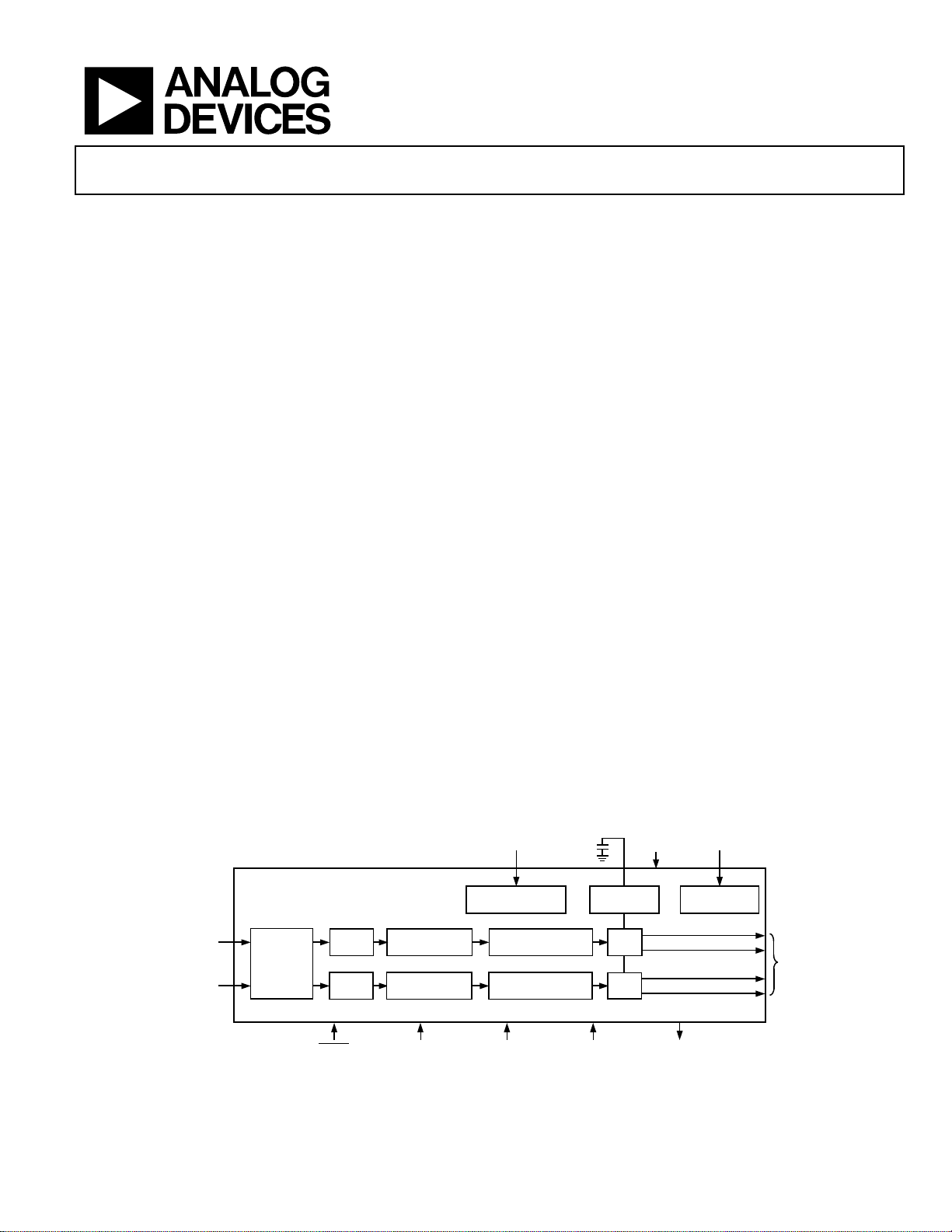
FUNCTIONAL BLOCK DIAGRAM
VOLUME
MUTE
AD1852
16-/18-/20-/24-BIT
DIGITAL
DATA INPUT
SERIAL
MODE
Rev. A
Information furnished by Analog Devices is believed to be accurate and reliable. However, no
responsibility is assumed by Analog Devices for its use, nor for any infringements of patents or other
rights of third parties that may result from its use. Specifications subject to change without notice. No
license is granted by implication or otherwise under any patent or patent rights of Analog Devices.
Trademarks and registered trademarks are the property of their respective owners.
2
SERIAL
DATA
INTERFACE
ATTEN/
ATTEN/
RESET
MUTE
MUTE
8 ×
f
S
INTERPOLATOR
f
8 ×
S
INTERPOLATOR
2
AUTO-CLOCK
DIVIDE CIRCUI T
22
ZERO
FLAG
CLOCK
IN
ANALOG
OUTPUTS
CONTROL DAT A
INPUT
3
SERIAL CONTROL
INTERFACE
MULTIBIT SIGMA-
DELTA MODUL AT OR
MULTIBIT SIGMA-
DELTA MODUL AT OR
DE-EMPHASISMUTE
Figure 1.
One Technology Way, P.O. Box 9106, Norwood, MA 02062-9106, U.S.A.
Tel: 781.329.4700 www.analog.com
Fax: 781.461.3113 ©2000–2009 Analog Devices, Inc. All rights reserved.
ANALOG
SUPPLY
DIGITAL
SUPPLY
VOLTAGE
REFERENCE
DAC
DAC
8457-001

AD1852
TABLE OF CONTENTS
Features .............................................................................................. 1
Applications ....................................................................................... 1
General Description ......................................................................... 1
Functional Block Diagram .............................................................. 1
Revision History ............................................................................... 2
Specifications ..................................................................................... 3
Analog Performance .................................................................... 3
Digital I/O (0°C to 70°C) ............................................................. 4
Temperature Range ...................................................................... 4
Power .............................................................................................. 4
Digital Filter Characteristics ....................................................... 4
Group Delay .................................................................................. 4
Digital Timing ............................................................................... 5
Absolute Maximum Ratings ............................................................ 6
Thermal Resistance ...................................................................... 6
ESD Caution .................................................................................. 6
Pin Configuration and Function Descriptions ............................. 7
Typical Performance Characteristics ..............................................9
Theory of Operation ...................................................................... 12
Serial Data Input Port ................................................................ 12
Serial Data Input Mode ............................................................. 12
Master Clock Autodivide Feature ............................................ 13
SPI Register Definitions ............................................................ 13
Register Addresses ...................................................................... 14
Volume Left and Volume Right Registers ............................... 14
SPI Timing................................................................................... 14
Mute ............................................................................................. 14
Control Register ......................................................................... 15
De-Emphasis ............................................................................... 15
Output Impedance ..................................................................... 15
Reset ............................................................................................. 15
Control Signals ........................................................................... 15
Outline Dimensions ....................................................................... 18
Ordering Guide .......................................................................... 18
REVISION HISTORY
11/09—Rev. 0 to Rev. A
Changes to Format ............................................................. Universal
Changes to Note 1 ............................................................................. 1
Changes to Table 2 ............................................................................ 3
Changes to Table 11 .......................................................................... 7
Changes to Register Addresses Section and Mute Section ....... 14
Changes to Figure 29 ...................................................................... 16
1/00—Revision 0: Initial Version
Rev. A | Page 2 of 20
AD1852
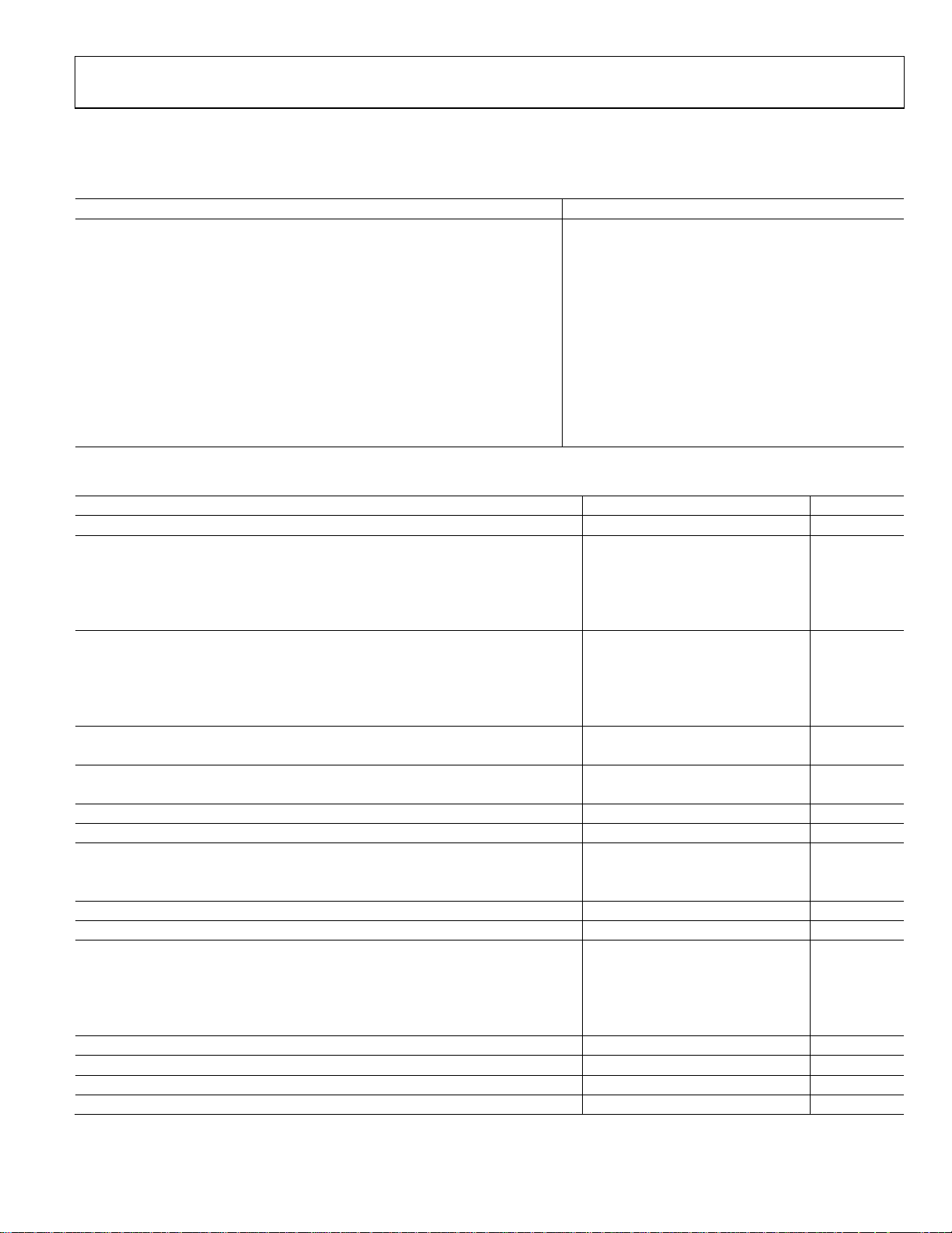
SPECIFICATIONS
Test conditions, unless otherwise noted.
Table 1.
Parameter Rating
Supply Voltages (AVDD, DVDD) 5.0 V
Ambient Temperature 25°C
Input Clock 24.576 MHz (512 × fS Mode)
Input Signal 996.11 Hz
−0.5 dB full scale
Input Sample Rate 48 kHz
Measurement Bandwidth 20 Hz to 20 kHz
Word Width 20 bits
Load Capacitance 100 pF
Load Impedance 47 kΩ
Input Voltage High 2.4 V
Input Voltage Low 0.8 V
ANALOG PERFORMANCE
Table 2.
Parameter1 Min Typ Max Unit
RESOLUTION 24 Bits
SIGNAL-TO-NOISE RATIO (20 Hz TO 20 kHz)
No Filter (Stereo) 112 dB
No Filter (Mono, See Figure 19) 115 dB
With A-Weighted Filter (Stereo) 114 dB
With A-Weighted Filter (Mono) 117 dB
DYNAMIC RANGE (20 Hz To 20 kHz, −60 dB INPUT)
No Filter (Stereo) 107 112 dB
No Filter (Mono, See Figure 24) 115 dB
With A-Weighted Filter (Stereo) 110 114 dB
With A-Weighted Filter (Mono) 117 dB
TOTAL HARMONIC DISTORTION + NOISE (STEREO) −94 −102 dB
0.00079 %
TOTAL HARMONIC DISTORTION + NOISE (MONO, SEE Figure 20) −105 dB
0.00056 %
TOTAL HARMONIC DISTORTION + NOISE (STEREO) VO = −20 dB −92 dB
TOTAL HARMONIC DISTORTION + NOISE (STEREO) VO = −60 dB −52 dB
ANALOG OUTPUTS
Differential Output Range (±Full Scale) 5.6 V p-p
Output Capacitance at Each Output Pin 2 pF
OUT-OF-BAND ENERGY (0.5 × fS TO 100 kHz) −90 dB
CMOUT 2.37 V
DC ACCURACY
Gain Error −10 ±2.0 +10 %
Interchannel Gain Mismatch −0.15 ±0.015 +0.15 dB
Gain Drift 150 250 ppm/°C
DC Offset −50 mV
INTERCHANNEL CROSSTALK (EIAJ METHOD) −120 dB
INTERCHANNEL PHASE DEVIATION ±0.1 Degrees
MUTE ATTENUATION −100 dB
DE-EMPHASIS GAIN ERROR ±0.1 dB
1
Performance of right and left channels is identical (exclusive of the Interchannel Gain Mismatch and Interchannel Phase Deviation specifications).
Rev. A | Page 3 of 20
AD1852
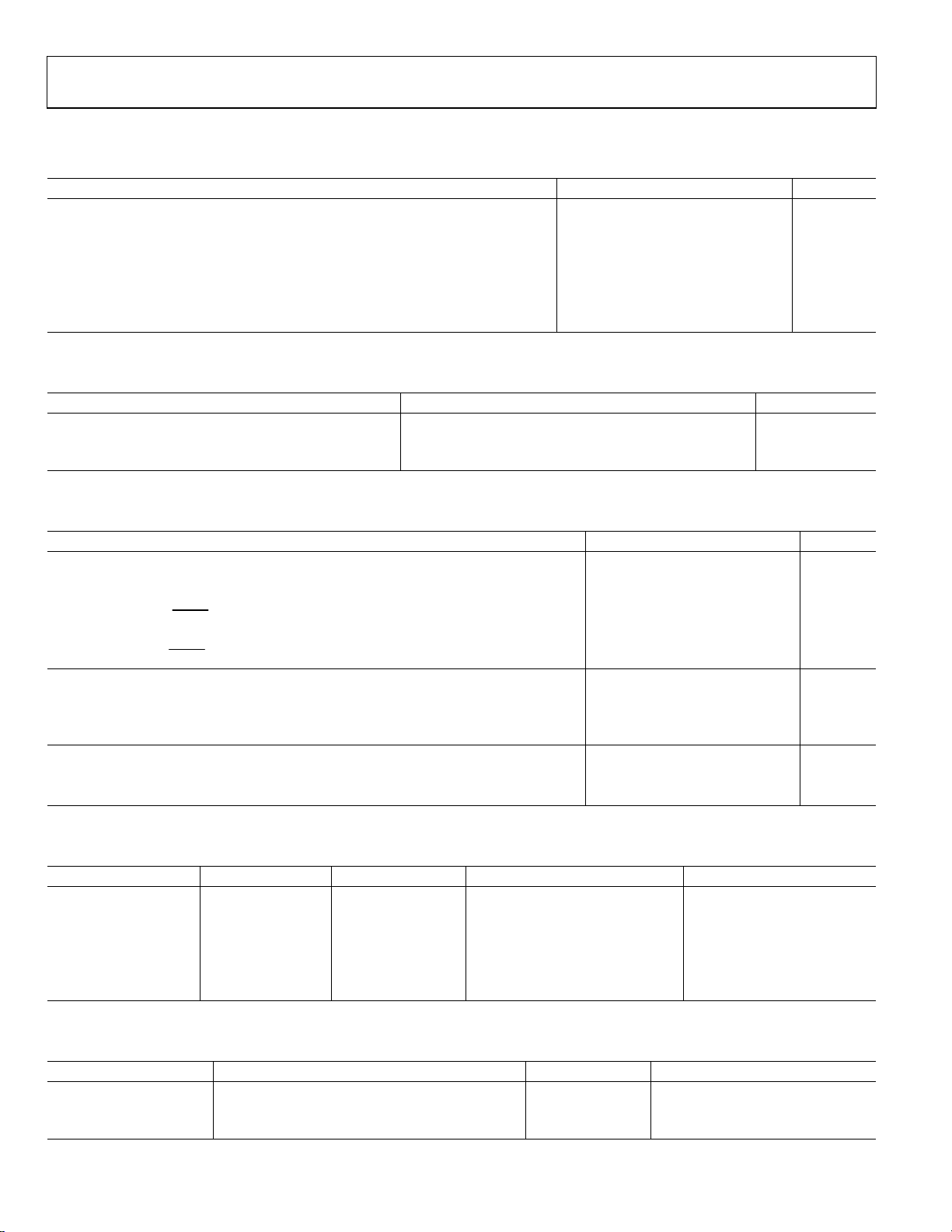
DIGITAL I/O (0°C TO 70°C)
Table 3.
Parameter Min Typ Max Unit
Input Voltage High (VIH) 2.2 V
Input Voltage Low (VIL) 0.8 V
Input Leakage (IIH at VIH = 2.4 V) 10 μA
Input Leakage (IIL at VIL = 0.8 V) 10 μA
High Level Output Voltage (VOH), IOH = 1 mA 2.0 V
Low Level Output Voltage (VOL), IOL = 1 mA 0.4 V
Input Capacitance 20 pF
TEMPERATURE RANGE
Table 4.
Parameter Min Typ Max Unit
Specifications Guaranteed 25 °C
Functionality Guaranteed 0 70 °C
Storage −55 +150 °C
POWER
Table 5.
Parameter Min Typ Max Unit
SUPPLIES
Voltage, Analog and Digital 4.50 5 5.50 V
Analog Current 33 40 mA
Analog Current—RESET
Digital Current 20 30 mA
Digital Current—RESET
DISSIPATION
Operation—Both Supplies 265 mW
Operation—Analog Supply 165 mW
Operation—Digital Supply 100 mW
POWER SUPPLY REJECTION RATIO
1 kHz, 300 mV p-p Signal at Analog Supply Pins −60 dB
20 kHz, 300 mV p-p Signal at Analog Supply Pins −50 dB
32 46 mA
27 37 mA
DIGITAL FILTER CHARACTERISTICS
Table 6.
Sample Rate (kHz) Pass Band (kHz) Stop Band (kHz) Stop-Band Attenuation (dB) Pass-Band Ripple (dB)
44.1 DC − 20 24.1 − 328.7 110 ±0.0002
48 DC − 21.8 26.23 − 358.28 110 ±0.0002
96 DC − 39.95 56.9 − 327.65 115 ±0.0005
192 DC − 87.2 117 − 327.65 95 +0/−0.04 (DC − 21.8 kHz)
+0/−0.5 (DC − 65.4 kHz)
+0/−1.5 (DC − 87.2 kHz)
GROUP DELAY
Table 7.
Chip Mode Group Delay Calculation fS (kHz) Group Delay (μs)
INT8× Mode 5553/(128 × fS) 48 903.8
INT4× Mode 5601/(64 × fS) 96 911.6
INT2× Mode 5659/(32 × fS) 192 921
Rev. A | Page 4 of 20

AD1852
DIGITAL TIMING
Guaranteed over 0°C to 70°C, AVDD = DVDD = 5.0 V × 10%.
Table 8.
Parameter Description Min Unit
t
MCLK period (f
DMP
t
MCLK low pulse width (all modes) 0.4 × t
DML
t
MCLK high pulse width (all modes) 0.4 × t
DMH
t
BCLK high pulse width (see Figure 26) 20 ns
DBH
t
BCLK low pulse width (see Figure 26) 20 ns
DBL
t
BCLK period (see Figure 26) 60 ns
DBP
t
LRCLK setup (see Figure 26) 20 ns
DLS
t
LRCLK hold (DSP serial port mode only) 5 ns
DLH
t
SDATA setup (see Figure 26) 5 ns
DDS
t
SDATA hold (see Figure 26) 10 ns
DDH
low pulse width
t
RSTL
1
Higher MCLK frequencies are allowable when using the on-chip master clock autodivide feature.
RESET
MCLK
= 256 × f
)1 54 ns
LRCLK
ns
DMP
ns
DMP
15
ns
Rev. A | Page 5 of 20
AD1852
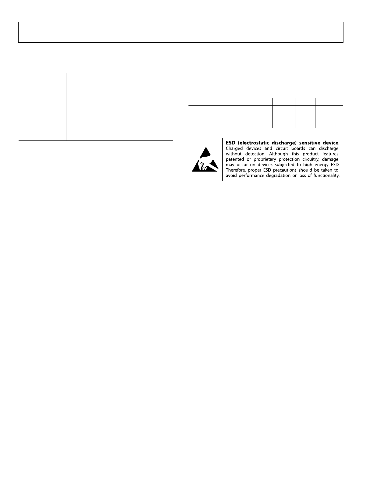
ABSOLUTE MAXIMUM RATINGS
Table 9.
Parameter Rating
DVDD to DGND −0.3 V to +6 V
AVDD to AGND −0.3 V to +6 V
Digital Inputs DGND − 0.3 V to DVDD + 0.3 V
Analog Outputs AGND − 0.3 V to AVDD + 0.3 V (see Figure 26)
AGND to DGND −0.3 V to +0.3 V
Reference Voltage (AVDD + 0.3 V)/2 V
Soldering 300°C
10 sec
Stresses above those listed under Absolute Maximum Ratings
may cause permanent damage to the device. This is a stress
rating only; functional operation of the device at these or any
other conditions above those indicated in the operational
section of this specification is not implied. Exposure to absolute
maximum rating conditions for extended periods may affect
device reliability.
THERMAL RESISTANCE
θJA is specified for the worst-case conditions, that is, a device
soldered in a circuit board for surface-mount packages.
Table 10.
Package Type θJA θJC Unit
Thermal Resistance
Junction-to-Ambient 109 °C/W
Junction-to-Case 39 °C/W
ESD CAUTION
Rev. A | Page 6 of 20
 Loading...