Analog Devices AD1836A Datasheet
FEATURES
5 V multichannel audio system
Accepts 16-/18-/20-/24-bit data
Supports 24-bit and 96 kHz sample rate
Multibit Σ-∆ modulators with data directed
scrambling
Differential output for optimum performance
ADCs: –92 dB THD + N, 105 dB SNR and dynamic range
DACs: –95 dB THD + N, 108 dB SNR and dynamic range
On-chip volume control with "auto-ramp" function
Programmable gain amplifier for ADC input
Hardware and software controllable clickless mute
Digital de-emphasis processing
Supports 256 × f
Power-down mode plus soft power-down mode
Flexible serial data port with right justified, left justified, I2S
compatible, and DSP serial port modes
TDM interface mode supports 8 in/8 out using a single
SHARC® SPORT
52-lead MQFP (PQFP) plastic package
, 512 × fS, or 768 × fS master clock
S
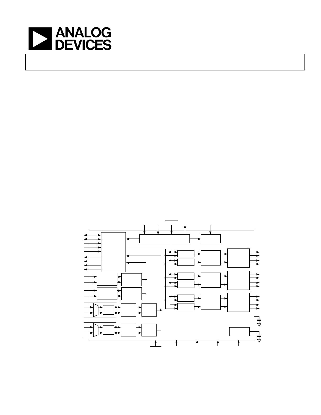
FUNCTIONAL BLOCK DIAGRAM
CCLK CDATA CLATCH
Multichannel 96 kHz Codec
AD1836A
APPLICATIONS
Home theater systems
Automotive audio systems
DVD recorders
Set-top boxes
Digital audio effects processors
PRODUCT OVERVIEW
The AD1836A is a high performance, single-chip codec that
provides three stereo DACs and two stereo ADCs using ADI’s
patented multibit Σ-∆ architecture. An SPI® port is included,
allowing a microcontroller to adjust volume and many other
parameters. The AD1836A operates from a 5 V supply, with
provision for a separate output supply to interface with low
voltage external circuitry. The AD1836A is available in a 52-lead
MQFP (PQFP) package.
COUT
MCLK
DLRCLK
DBCLK
DSDATA1
DSDATA2
DSDATA3
ALRCLK
ABCLK
ASDATA1
ASDATA2
ADC1L
ADC1R
CAPL1
ADC2L1
ADC2L2
CAPL2
CAPR1
ADC2R1
ADC2R2
CAPR2
Rev. 0
Information furnished by Analog Devices is believed to be accurate and reliable.
However, no responsibility is assumed by Analog Devices for its use, nor for any
infringements of patents or other rights of third parties that may result from its use.
Specifications subject to change without notice. No license is granted by implication
or otherwise under any patent or patent rights of Analog Devices. Trademarks and
registered trademarks are the property of their respective owners.
SERIAL
DATA
I/O
PORT
Σ-∆
ADC1L
48kHz/96kHz
Σ-∆
ADC1R
48kHz/96kHz 48kHz/96kHz
PGA
MUX
PGA
MUX
DIGITAL
FILTER
48kHz/96kHz
DIGITAL
FILTER
Σ-∆
ADC2L
48kHz
Σ-∆
ADC2R
48kHz
CONTROL PORT
DIGITAL
FILTER
48kHz
DIGITAL
FILTER
48kHz
PD/RST AVDD AGND DVDD DGND
Figure 1.
CLOCK
VOLUME
VOLUME
VOLUME
VOLUME
VOLUME
VOLUME
2432
DIGITAL
FILTER
DIGITAL
FILTER
DIGITAL
FILTER
Σ-∆
DAC
Σ-∆
DAC
Σ-∆
DAC
V
REF
DAC1L
DAC1R
DAC2L
DAC2R
DAC3L
DAC3R
FILTD
FILTR
One Technology Way, P.O. Box 9106, Norwood, MA 02062-9106, U.S.A.
Tel: 781.329.4700 www.analog.com
Fax: 781.326.8703 © 2003 Analog Devices, Inc. All rights reserved.

AD1836A
TABLE OF CONTENTS
AD1836A—Specifications............................................................... 3
Serial Control Port ..................................................................... 12
Absolute Maximum Ratings............................................................ 8
Pin Configuration And Pin Functional Descriptions.................. 9
Functional Overview...................................................................... 11
ADCs............................................................................................ 11
DACs............................................................................................ 11
Clock Signals............................................................................... 11
Reset and Power-Down ............................................................. 12
REVISION HISTORY
Revision 0: Initial Version
Power Supply and Voltage Reference....................................... 13
Serial Data Ports—Data Format............................................... 13
SPI Control Registers................................................................. 19
Outline Dimensions....................................................................... 23
ESD Caution................................................................................ 23
Ordering Guide .......................................................................... 23
Rev. 0 | Page 2 of 24

AD1836A
AD1836A—SPECIFICATIONS
Table 1. Test conditions, unless otherwise noted. Performance of all channels is identical (exclusive of the Interchannel Gain
Mismatch and Interchannel Phase Deviation specifications).
Parameter Rating
Supply Voltages (AVDD, DVDD) 5 V
Ambient Temperature 25°C
Master Clock 12.288 MHz (48 kHz fS, 256 × fS Mode)
Input Signal 1.000 kHz, 0 dBFS (Full Scale)
Input Sample Rate 48 kHz
Measurement Bandwidth 20 Hz to 20 kHz
Word Width 24 Bits
Load Capacitance (Digital Output) 100 pF
Load Impedance (Digital Output) 2.5 kΩ
Input Voltage HI 2.4 V
Input Voltage LO 0.8 V
Rev. 0 | Page 3 of 24
AD1836A
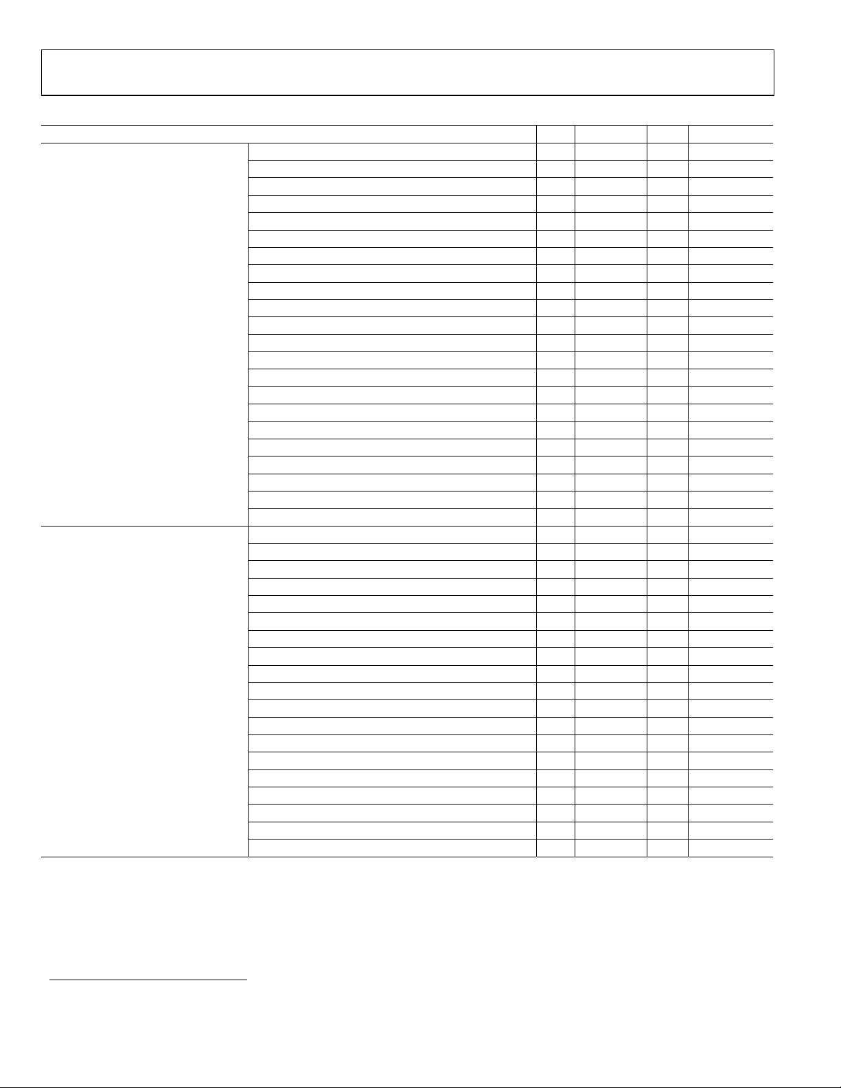
Table 2. Analog Performance
Parameter Min Typ Max Unit
ANALOG-TO-DIGITAL CONVERTERS
DIGITAL-TO-ANALOG CONVERTERS
ADC Resolution (all ADCs) 24 Bits
Dynamic Range (20 Hz to 20 kHz, –60 dB Input)
No Filter (RMS), AD1836AAS 97 102 dB
With A-Weighted Filter (RMS), AD1836AAS 100 105 dB
No Filter (RMS), AD1836ACS 94 99 dB
With A-Weighted Filter (RMS), AD1836ACS 97 102 dB
Total Harmonic Distortion + Noise (–1 dBFS)1 –92 –83 dB
Full-Scale Input Voltage (Differential) 2.18 (6.16) V rms (V pp)
Gain Error –5.0 +5.0 %
Interchannel Gain Mismatch –0.1 +0.1 dB
Offset Error –10 0 +10 mV
Gain Drift 100 ppm/°C
Interchannel Isolation –110 dB
Programmable Input Gain 12 dB
Gain Step Size 3 dB
CMRR, Direct Input, 100 mV RMS, 1 kHz –77 –63 dB
CMRR, Direct Input, 100 mV RMS, 20 kHz –72 –60 dB
CMRR, PGA Differential Input, 100 mV RMS, 1 kHz –57 –39 dB
CMRR, PGA Differential Input, 100 mV RMS, 20 kHz –57 –39 dB
Input Resistance 10 kΩ
Input Capacitance 15 pF
Common-Mode Input Volts 2.25 V
Dynamic Range (20 Hz to 20 kHz, –60 dB Input)
No Filter (RMS), AD1836AAS 102 105 dB
With A-Weighted Filter (RMS), AD1836AAS 105 108 dB
No Filter (RMS), AD1836ACS 99 102 dB
With A-Weighted Filter (RMS), AD1836ACS 102 105 dB
Total Harmonic Distortion + Noise (0 dBFS)1 –95 –85 dB
Full-Scale Output Voltage (Differential) 2.0 (5.6) V rms (V pp)
Gain Error –6.0 +6.0 %
Interchannel Gain Mismatch –0.3 +0.3 dB
Offset Error 15 55 95 mV
Gain Drift 150 ppm/°C
Interchannel Isolation –110 dB
Interchannel Phase Deviation ±0.1 Degrees
Volume Control Step Size (1023 Linear Steps) 0.098 %
Volume Control Range (Max Attenuation) 60 dB
Max Attenuation –100 dB
De-emphasis Gain Error ±0.1 dB
Output Resistance at Each Pin 115 Ω
V
(FILTR), Common-Mode Output 2.2 2.25 2.3 V
REF
1, 2
1, 2
1
Total harmonic distortion + noise and dynamic range typical specifications are for two channels active, max/min are all channels active.
2
Measured with Audio Precision System Two Cascade in rms mode. Averaging mode will show approximately 2 dB better performance.
Rev. 0 | Page 4 of 24
AD1836A
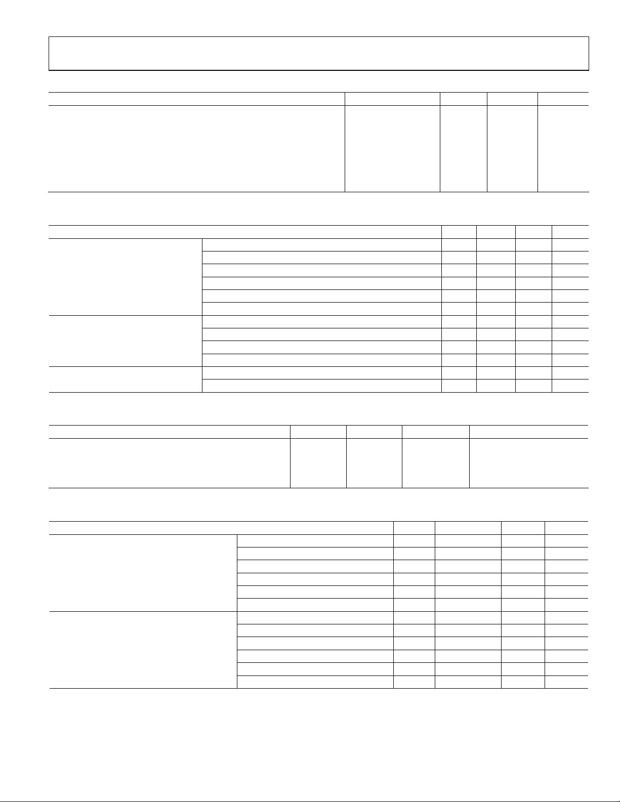
Table 3. Digital I/O
Parameter Min Typ Max Unit
Input Voltage HI (VIH) 2.2 V
Input Voltage LO (VIL) 0.8 V
Input Leakage (IIH @ VIH = 2.4 V) 10 µA
Input Leakage (IIL @ VIL = 0.8 V) 10 µA
High Level Output Voltage (VOH) IOH = 2 mA ODVDD – 0.4 V
Low Level Output Voltage (VOL) IOL = 2 mA 0.5 V
Input Capacitance 20 pF
Table 4. Power Supplies
Parameter Min Typ Max Unit
Voltage, DVDD and AVDD 4.75 5 5.25 V
Voltage, ODVDD 3.0 3.3/5 5.25 V
Supplies
Dissipation
Power Supply Rejection Ratio
Table 5. Temperature Range
Parameter Min Typ Max Unit
Specifications Guaranteed 25 °C
Functionality Guaranteed
Storage –65 +150 °C
Table 6. Digital Filter @ 44.1 kHz
Parameter Min Typ Max Unit
ADC DECIMATION FILTER
DAC INTERPOLATION FILTER
Analog Current 108 mA
Analog Current—Power-Down 47 mA
Digital Current 78 mA
Digital Current—Power-Down 1.5 mA
Operation—Both Supplies 930 mW
Operation—Analog Supplies 540 mW
Operation—Digital Supplies 390 mW
Power-Down—Both Supplies 243 mW
1 kHz 300 mV p-p Signal at Analog Supply Pins –60 dB
20 kHz 300 mV p-p Signal at Analog Supply Pins –50 dB
–40 +85 °C Ambient
–40 +110 °C Case
Pass Band 20 kHz
Pass-Band Ripple ±0.0001 dB
Transition Band 22 kHz
Stop Band 24 kHz
Stop-Band Attenuation 120 dB
Group Delay 990.20 µs
Pass Band 20 kHz
Pass-Band Ripple ±0.01 dB
Transition Band 22 kHz
Stop Band 24 kHz
Stop-Band Attenuation 70 dB
Group Delay 446.35 µs
Rev. 0 | Page 5 of 24
AD1836A
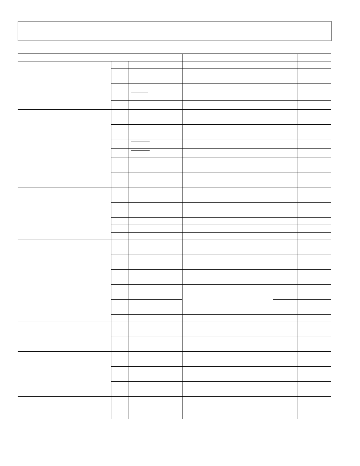
Table 7. Timing Specifications
Parameter Comments Min Max Unit
tMH MCLK High 512 × fS Mode 18 ns
tML MCLK Low 512 × fS Mode 18 ns
t
MCLK Period 512 × fS Mode 36 ns
MASTER CLOCK AND RESET
SPI PORT
DAC SERIAL PORT
(Normal Modes)
DAC SERIAL PORT
(Packed 128 Mode, Packed 256 Mode)
ADC SERIAL PORT
(Normal Modes)
ADC SERIAL PORT
(Packed 128 Mode, Packed 256 Mode)
ADC SERIAL PORT
(TDM Packed AUX)
AUXILIARY INTERFACE
MCLK
f
MCLK Frequency 512 × fS Mode 27 MHz
MCLK
t
PDR
t
PDRR
t
CCLK High 10 ns
CHH
t
CCLK Low 10 ns
CHL
t
CDATA Setup To CCLK Rising 5 ns
CDS
t
CDATA Hold From CCLK Rising 5 ns
CDH
t
CLS
t
CLH
t
COUT Enable From CCLK Falling 10 ns
CODE
t
COUT Delay From CCLK Falling 10 ns
COD
t
COUT Hold From CCLK Falling 0 ns
COH
t
COUT Three-State From CCLK Falling 10 ns
COTS
t
DBCLK High 15 ns
DBH
t
DBCLK Low 15 ns
DBL
PD/RST
PD/RST
CLATCH
CLATCH
Low
Recovery
Setup
Hold
5 ns
Reset to Active Output 4500 t
MCLK
To CCLK Rising 5 ns
From CCLK Falling 5 ns
fDB DBCLK Frequency 64 × fS ns
t
DLRCLK Setup To DBCLK Rising 0 ns
DLS
t
DLRCLK Hold From DBCLK Rising 10 ns
DLH
t
DSDATA Setup To DBCLK Rising 0 ns
DDS
DSDATA Hold From DBCLK Rising 20 ns
t
DDH
t
DBCLK High 15 ns
DBH
t
DBCLK Low 15 ns
DBL
fDB DBCLK Frequency 256 × fS ns
t
DLRCLK Setup To DBCLK Rising 0 ns
DLS
t
DLRCLK Hold From DBCLK Rising 10 ns
DLH
t
DSDATA Setup To DBCLK Rising 0 ns
DDS
DSDATA Hold From DBCLK Rising 20 ns
t
DDH
t
ABCLK Delay 15 ns
ABD
t
LRCLK Skew From ABCLK Falling –2 +2 ns
ALS
ASDATA Delay From ABCLK Falling 5 ns
t
ABDD
t
ABCLK Delay 15 ns
ABD
t
LRCLK Skew From ABCLK Falling –2 +2 ns
ALS
ASDATA Delay From ABCLK Falling 5 ns
t
ABDD
t
ABCLK Delay 15 ns
ABD
t
LRCLK Skew From ABCLK Falling –2 +2 ns
ALS
t
ASDATA Delay From ABCLK Falling 5 ns
ABDD
t
DSDATA1 Hold To ABCLK Rising 0 ns
DDS
DSDATA1 Hold From ABCLK Rising 7 ns
t
DDH
t
AAUXDATA Setup To AUXBCLK Rising 7 ns
AXDS
t
AAUXDATA Hold From AUXBCLK Rising 10 ns
AXDH
t
DAUXDATA Delay From AUXBCLK Falling 25 ns
DXDD
From MCLK Transition, 256 × f
From MCLK Rising, 512 × f
Mode
S
From MCLK Transition, 256 × f
From MCLK Rising, 512 × f
S
From MCLK Transition, 256 × f
From MCLK Rising, 512 × f
Mode
S
Mode
S
Mode
S
Mode
Mode
S
Rev. 0 | Page 6 of 24
AD1836A
Table 7. Timing Specifications (Continued)
Parameter Comments Min Max Unit
AUXILIARY INTERFACE
(Master Mode)
AUXILIARY INTERFACE
(Slave Mode)
t
AUXBCLK Delay 15 ns
XBD
AUXLRCLK Skew From AUXBCLK Falling –3 +3 ns
t
XLS
t
AUXBCLK High 60 ns
XBH
t
AUXBCLK Low 60 ns
XBL
fXB AUXBCLK Frequency 64 × fS ns
t
AUXLRCLK Setup To AUXBCLK Rising 5 ns
DLS
AUXLRCLK Hold From AUXBCLK Rising 15 ns
t
DLH
From MCLK Transition, 256 × f
From MCLK Rising, 512 × f
Mode
S
Mode
S
Rev. 0 | Page 7 of 24

AD1836A
ABSOLUTE MAXIMUM RATINGS
Table 8. AD1836A Absolute Maximum Ratings
Parameter Min Max Unit
Analog (AVDD) –0.3 +6 V
Digital (DVDD) –0.3 +6 V
Input Current (Except Supply Pins) ±20 mA
Analog Input Voltage (Signal Pins) –0.3 AVDD + 0.3 V
Digital Input Voltage (Signal Pins) –0.3 DVDD + 0.3 V
Ambient Temperature (Operating) –40 +85 °C
Stresses above those listed under Absolute Maximum Ratings may cause permanent damage to the device. This is a stress rating only and
functional operation of the device at these or any other condition s above those indicated in the operational section of this specification is
not implied. Exposure to absolute maximum rating conditions may affect device reliability.
Table 9. Package Characteristics
Parameter Min Typ Max Unit
θJA (Thermal Resistance [Junction to Ambient])
θJC (Thermal Resistance [Junction to Case])
45 °C/W
18 °C/W
Rev. 0 | Page 8 of 24
 Loading...