Analog Devices AD1835 b Anomaly Datasheet

2 ADC, 8 DAC,
T
T
96 kHz, 24-Bit - Codec
Silicon Anomaly Sheet
AD1835
This document details known bugs in the current version of the AD1835.
Analog Devices, Inc. is committed, through future silicon revisions, to continuously improve silicon functionality.
The bugs described in this document have been fixed in the A version of this part (AD1835A).
Analog Devices, Inc. will use its best endeavors to ensure that these future silicon revisions remain compatible with your present
software/systems implementing the recommended workarounds outlined in this document.
ADC Phase Shift Bug
The ADC engine used in the AD1835 loads the serial port with the results of the last conversion periodically at the sample rate. The
loading operation is initially determined by where the PD/RST pin goes high. For slave mode operation, the loading operation and
LRCLK or FSTDM signal have no fixed relationship so it is possible that the loading operation can occur in the middle of a data
transfer. This results in the right ADC sample being one sample ahead of the left ADC sample, which presents itself as a phase shift.
See Figure 1.
1ST SAMPLE 2ND SAMPLE 3RD SAMPLE
FSTDM
ASDATA
LEFT (n) RIGHT (n+1) LEFT (n+1) RIGHT (n+2) LEFT (n+2) RIGHT (n+3)
*TIMESLOTS NOT TO SCALE
Figure 1. Phase Shift Bug
Workaround
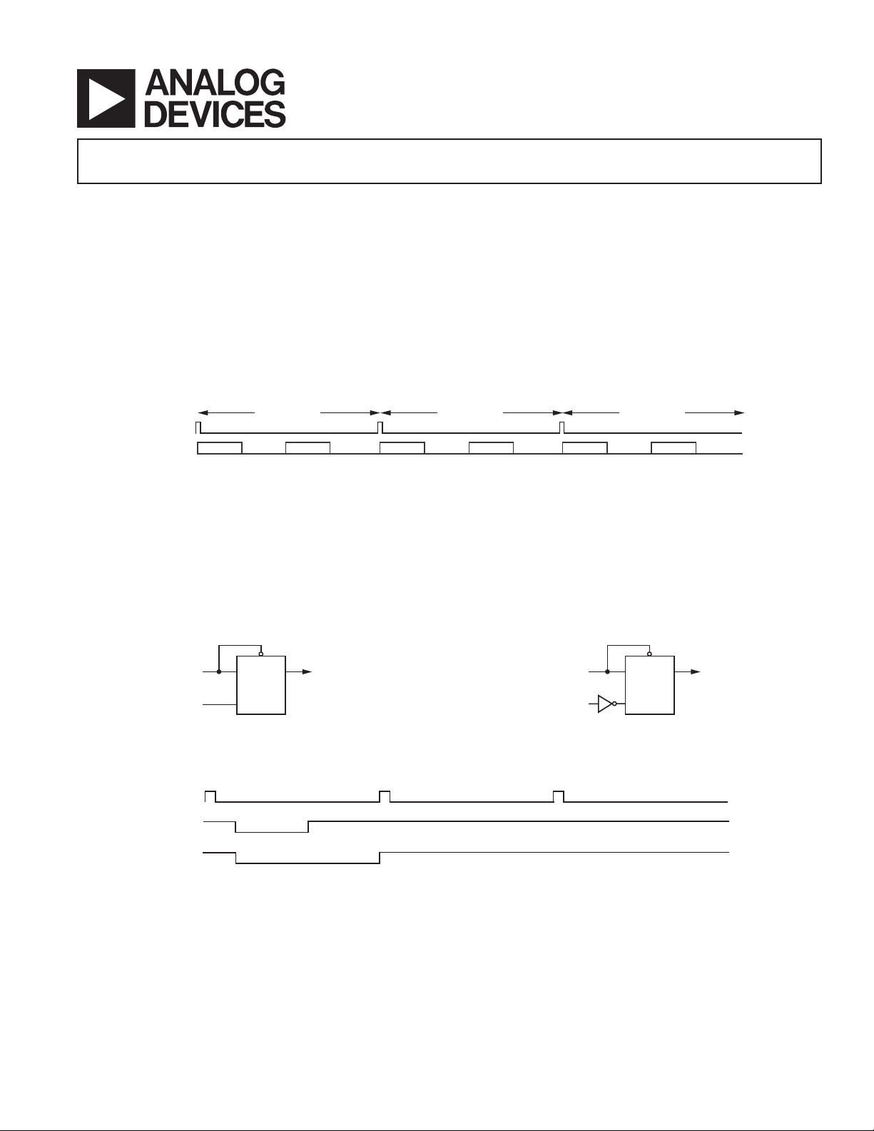
Synchronizing the rising edge of PD/RST with the appropriate LRCLK (for I2S, left or right justified modes) or FSTDM (for
TDM256 mode) edge will ensure that the ADC result updates occur in a safe region and the phase shift will not occur. Figure 2
shows a synchronization circuit using a single flip-flop that latches the reset signal on the rising edge of FSTDM/ALRCLK. Figure 3
shows an alternate circuit for latching the reset on the falling edge of ALRCLK. Figure 4 shows a timing diagram associated with
Figure 2. Table I lists the ADC modes affected by this issue and which circuit should be used to prevent it occurring.
RESET
FSTDM/
ALRCLK
D
CLK
CLR
AD1835
Q
PD/RS
Figure 2. Synchronization Circuit for Rising Edges
FSTDM
RESET
AD183x
RESET
*PROPAGATION DELAYS NOT SHOWN
Figure 4. Reset Synchronized to Rising Edge of FSTDM/ALRCLK
REV. B
Information furnished by Analog Devices is believed to be accurate and
reliable. However, no responsibility is assumed by Analog Devices for its
use, nor for any infringements of patents or other rights of third parties that
may result from its use. No license is granted by implication or otherwise
under any patent or patent rights of Analog Devices. Trademarks and
registered trademarks are the property of their respective owners.
RESET
ALRCLK
D
CLK
CLR
AD1835
Q
PD/RS
Figure 3. Synchronization Circuit for Falling Edges
One Technology Way, P.O. Box 9106, Norwood, MA 02062-9106, U.S.A.
Tel: 781/329-4700 www.analog.com
Fax: 781/326-8703 © 2004 Analog Devices, Inc. All rights reserved.

AD1835
Table I. Safe Regions for PD/RST Rising Edge
ADC Mode Safe Region Recommended Circuit
2
I
SOn rising edge of ALRCLK Figure 2
Left Justified On falling edge of ALRCLK Figure 3
Right Justified On rising edge of ALRCLK Figure 2
TDM256 On rising edge of FSTDM Figure 2
96 kHz Operation
When it is required to operate the AD1835 in 96 kHz mode, two write operations are required to the SPI registers to program
the IMCLK divider and the ADC sample rate. Programming these two registers can also cause the phase shift error.
Workaround
To guarantee proper operation, programming these registers should occur during the internal reset time. The internal reset time is
3072 MCLK periods from the rising edge of PD/RST (approximately 12 sample intervals).
ADC Power-Down via SPI Register
Powering the ADCs down and then back up will cause the ADC engine to begin updating the ADC results periodically at the sample
rate. Since SPI writes are typically asychronous to the ADC FSTDM/ALRCLK signals, it is possible that the updates can occur in a
region that will cause the previously described phase shift issue. It is therefore recommended that the ADC power-down bit not be
used when the AD1835 ADC is operated in slave mode.
TDM256 Master Mode—ADC Section
When the AD1835 is operated in TDM256 master mode, the phase shift error is always present. Since the AD1835 generates the
FSTDM signal after a reset, it is not possible to synchronize these two signals.
Workaround
Since no data is actually lost, the phase relationship can be reestablished in the DSP or other controller under software control.
DAC Writes
When a write to one of the DAC registers is generated, an internal strobe pulse is used to indicate that the write is finished and the
contents of the serial shift register can be loaded to the DAC register. On rare occasions the relationship between the rising edge of
CLATCH and the MCLK can cause this pulse not to be generated and the write to the register is ignored.
Workaround
Writing the same value to the DAC twice will ensure that the register gets updated correctly.
S02665–0–7/04(B)
–2–
REV. B
 Loading...