


AMIC A29L400UV-90U, A29L400UV-90, A29L400UV, A29L400UM-90, A29L400UM Datasheet
...A29L400 Series
512K X 8 Bit / 256K X 16 Bit CMOS 3.0 Volt-only,
Preliminary |
Boot Sector Flash Memory |
|
|
Features
nSingle power supply operation
-Full voltage range: 2.7 to 3.6 volt read and write operations for battery-powered applications
-Regulated voltage range: 3.0 to 3.6 volt read and write operations for compatibility with high performance 3.3 volt microprocessors
nAccess times:
-70/90 (max.)
nCurrent:
-4 mA typical active read current
-20 mA typical program/erase current
-200 nA typical CMOS standby
-200 nA Automatic Sleep Mode current
nFlexible sector architecture
-16 Kbyte/ 8 KbyteX2/ 32 Kbyte/ 64 KbyteX7 sectors
-8 Kword/ 4 KwordX2/ 16 Kword/ 32 KwordX7 sectors
-Any combination of sectors can be erased
-Supports full chip erase
-Sector protection:
A hardware method of protecting sectors to prevent any inadvertent program or erase operations within that sector. Temporary Sector Unprotect feature allows code changes in previously locked sectors
nExtended operating temperature range: -45°C ~ +85°C for –U series
nUnlock Bypass Program Command
-Reduces overall programming time when issuing multiple program command sequence
nTop or bottom boot block configurations available
nEmbedded Algorithms
-Embedded Erase algorithm will automatically erase the entire chip or any combination of designated sectors and verify the erased sectors
-Embedded Program algorithm automatically writes and verifies data at specified addresses
nTypical 100,000 program/erase cycles per sector
n20-year data retention at 125°C
-Reliable operation for the life of the system
nCompatible with JEDEC-standards
-Pinout and software compatible with single-power- supply Flash memory standard
-Superior inadvertent write protection
nData Polling and toggle bits
-Provides a software method of detecting completion of program or erase operations
nReady / BUSY pin (RY / BY )
-Provides a hardware method of detecting completion of program or erase operations (not available on 44pin SOP)
nErase Suspend/Erase Resume
-Suspends a sector erase operation to read data from, or program data to, a non-erasing sector, then resumes the erase operation
nHardware reset pin (RESET )
-Hardware method to reset the device to reading array data
nPackage options
-44-pin SOP or 48-pin TSOP (I) or 48-ball TFBGA
PRELIMINARY (October, 2002, Version 0.2) |
1 |
AMIC Technology, Inc. |

A29L400 Series
General Description
The A29L400 is an 4Mbit, 3.0 volt-only Flash memory organized as 524,288 bytes of 8 bits or 262,144 words of 16 bits each. The 8 bits of data appear on I/O0 - I/O7; the 16 bits of data appear on I/O0~I/O15. The A29L400 is offered in 48ball TFBGA, 44-pin SOP and 48-Pin TSOP packages. This device is designed to be programmed in-system with the standard system 3.0 volt VCC supply. Additional 12.0 volt VPP is not required for in-system write or erase operations. However, the A29L400 can also be programmed in standard EPROM programmers.
The A29L400 has the first toggle bit, I/O6, which indicates whether an Embedded Program or Erase is in progress, or it is in the Erase Suspend. Besides the I/O6 toggle bit, the A29L400 has a second toggle bit, I/O2, to indicate whether the addressed sector is being selected for erase. The A29L400 also offers the ability to program in the Erase Suspend mode. The standard A29L400 offers access times of 70 and 90ns, allowing high-speed microprocessors to operate without wait states. To eliminate bus contention the
device has separate chip enable ( CE ), write enable ( WE )
and output enable ( OE ) controls.
The device requires only a single 3.0 volt power supply for both read and write functions. Internally generated and regulated voltages are provided for the program and erase operations.
The A29L400 is entirely software command set compatible with the JEDEC single-power-supply Flash standard. Commands are written to the command register using standard microprocessor write timings. Register contents serve as input to an internal state-machine that controls the erase and programming circuitry. Write cycles also internally latch addresses and data needed for the programming and erase operations. Reading data out of the device is similar to reading from other Flash or EPROM devices.
Device programming occurs by writing the proper program command sequence. This initiates the Embedded Program algorithm - an internal algorithm that automatically times the program pulse widths and verifies proper program margin.
Device erasure occurs by executing the proper erase command sequence. This initiates the Embedded Erase algorithm - an internal algorithm that automatically preprograms the array (if it is not already programmed) before executing the erase operation. During erase, the device automatically times the erase pulse widths and verifies proper erase margin. The Unlock Bypass mode facilitates faster programming times by requiring only two write cycles to program data instead of four.
The host system can detect whether a program or erase
operation is complete by observing the RY / BY pin, or by
reading the I/O7 (Data Polling) and I/O6 (toggle) status bits. After a program or erase cycle has been completed, the device is ready to read array data or accept another command.
The sector erase architecture allows memory sectors to be erased and reprogrammed without affecting the data contents of other sectors. The A29L400 is fully erased when shipped from the factory.
The hardware sector protection feature disables operations for both program and erase in any combination of the sectors of memory. This can be achieved via programming equipment.
The Erase Suspend/Erase Resume feature enables the user to put erase on hold for any period of time to read data from, or program data to, any other sector that is not selected for erasure. True background erase can thus be achieved.
The hardware RESET pin terminates any operation in progress and resets the internal state machine to reading
array data. The RESET pin may be tied to the system reset circuitry. A system reset would thus also reset the device, enabling the system microprocessor to read the boot-up firmware from the Flash memory.
The device offers two power-saving features. When addresses have been stable for a specified amount of time, the device enters the automatic sleep mode. The system can also place the device into the standby mode. Power consumption is greatly reduced in both these modes.
PRELIMINARY (October, 2002, Version 0.2) |
2 |
AMIC Technology, Inc. |

A29L400 Series
Pin Configurations |
|
|
|
|
|
||
n SOP |
|
|
|
|
|
n TSOP (I) |
|
NC |
1 |
|
44 |
RESET |
|
|
|
RY/BY |
2 |
|
43 |
WE |
|
|
|
A17 |
3 |
|
42 |
A8 |
A15 |
1 |
|
A7 |
4 |
|
41 |
A9 |
A14 |
2 |
|
|
A13 |
3 |
|
||||
|
|
|
|
|
|
||
A6 |
5 |
|
40 |
A10 |
A12 |
4 |
|
A5 |
6 |
|
39 |
A11 |
A11 |
5 |
|
|
A10 |
6 |
|
||||
|
|
|
|
|
|
||
A4 |
7 |
|
38 |
A12 |
A9 |
7 |
|
A3 |
8 |
|
37 |
A13 |
A8 |
8 |
|
|
NC |
9 |
|
||||
|
|
|
|
|
|
||
A2 |
9 |
A29L400 |
36 |
A14 |
NC |
10 |
|
A1 |
10 |
35 |
A15 |
WE |
11 |
|
|
|
RESET |
12 |
A29L400V |
||||
|
|
|
|
|
|||
A0 |
11 |
|
34 |
A16 |
NC |
13 |
|
|
|
||||||
CE |
12 |
|
33 |
BYTE |
NC |
14 |
|
|
RY/BY |
15 |
|
||||
VSS |
13 |
|
32 |
VSS |
NC |
16 |
|
OE |
14 |
|
31 |
I/O15 (A-1) |
A17 |
17 |
|
|
A7 |
18 |
|
||||
|
|
|
|
|
|
||
I/O0 |
15 |
|
30 |
I/O7 |
A6 |
19 |
|
I/O8 |
16 |
|
29 |
I/O14 |
A5 |
20 |
|
|
A4 |
21 |
|
||||
|
|
|
|
|
|
||
I/O1 |
17 |
|
28 |
I/O6 |
A3 |
22 |
|
I/O9 |
18 |
|
27 |
I/O13 |
A2 |
23 |
|
|
A1 |
24 |
|
||||
|
|
|
|
|
|
||
I/O2 |
19 |
|
26 |
I/O5 |
|
|
|
I/O10 |
20 |
|
25 |
I/O12 |
|
|
|
I/O3 |
21 |
|
24 |
I/O4 |
|
|
|
I/O11 |
22 |
|
23 |
VCC |
|
|
|
n TFBGA
TFBGA
Top View, Balls Facing Down
A6 |
B6 |
C6 |
D6 |
E6 |
F6 |
G6 |
H6 |
A13 |
A12 |
A14 |
A15 |
A16 |
BYTE |
I/O15(A-1) VSS |
|
A5 |
B5 |
C5 |
D5 |
E5 |
F5 |
G5 |
H5 |
A9 |
A8 |
A10 |
A11 |
I/O7 |
I/O14 |
I/O13 |
I/O6 |
A4 |
B4 |
C4 |
D4 |
E4 |
F4 |
G4 |
H4 |
WE |
RESET |
NC |
NC |
I/O5 |
I/O12 |
VCC |
I/O4 |
A3 |
B3 |
C3 |
D3 |
E3 |
F3 |
G3 |
H3 |
RY/BY |
NC |
NC |
NC |
I/O2 |
I/O10 |
I/O11 |
I/O3 |
A2 |
B2 |
C2 |
D2 |
E2 |
F2 |
G2 |
H2 |
A7 |
A17 |
A6 |
A5 |
I/O0 |
I/O8 |
I/O9 |
I/O1 |
A1 |
B1 |
C1 |
D1 |
E1 |
F1 |
G1 |
H1 |
A3 |
A4 |
A2 |
A1 |
A0 |
CE |
OE |
VSS |
48  A16
A16
47  BYTE
BYTE
46  VSS
VSS
45  I/O15 (A-1)
44  I/O7
I/O7
43  I/O14
I/O14
42  I/O6
I/O6
41  I/O13
I/O13
40  I/O5
I/O5
39  I/O12
I/O12
38  I/O4
I/O4
37  VCC
VCC
36  I/O11
I/O11
35  I/O3
I/O3
34  I/O10
I/O10
33  I/O2
I/O2
32  I/O9
I/O9
31  I/O1
I/O1
30  I/O8
I/O8
29  I/O0
I/O0
28  OE
OE
27  VSS
VSS
26  CE
CE
25  A0
A0
PRELIMINARY (October, 2002, Version 0.2) |
3 |
AMIC Technology, Inc. |
A29L400 Series
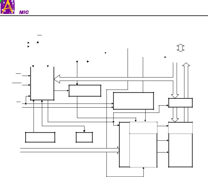
Block Diagram
RY/BY
|
VCC |
|
|
|
|
|
|
|
|
|
|
|
|
|
|
|
I/O0 - I/O 15 (A-1) |
||
|
|
|
|
|
|
|
|
|
|
|
|
|
|
|
|
|
|
||
|
VSS |
|
|
|
|
|
|
|
|
|
|
|
|
|
|
|
|
|
|
|
|
|
|
|
|
|
|
|
|
Sector Switches |
|
|
|
|
|
|
|||
|
|
|
|
|
|
|
|
|
|
|
|
|
|
|
|
||||
|
|
|
|
|
|
|
|
|
|
|
|
|
|
|
|
|
|
|
|
|
|
|
|
|
|
|
|
|
|
|
|
|
|
|
|
|
|
Input/Output |
|
|
|
|
|
|
|
|
|
|
|
|
|
Erase Voltage |
|
|
|
|
Buffers |
|
|
RESET |
|
|
|
|
|
|
|
|
|
|
|
|
|
||||||
|
|
|
|
|
|
|
|
|
|
|
|
Generator |
|
|
|
|
|
|
|
|
|
|
|
|
|
|
|
|
|
|
|
|
|
|
|
|
|
|
|
|
|
|
|
|
|
|
|
|
|
|
|
|
|
|
|
|
|
|
|
WE |
State |
|
|
|
|
|
|
Control |
|
|
|
|
|
|
|
|
|
|
|
|
|
|
|
BYTE |
|
PGM Voltage |
|
|
|
|
|
|
Command |
|
|
|
|
|
|
|
Register |
Generator |
|
Chip Enable |
|
|
|
|
|
|
|
|
|
||
CE |
|
|
|
Output Enable |
STB |
Data Latch |
|
|
|
|
|
Logic |
|||
|
|
|
|
|
|
||
OE |
|
|
|
|
|
|
|
|
|
|
|
|
|
|
|
|
|
|
STB |
|
Y-Decoder |
|
Y-Gating |
|
|
|
Latch |
|
|
|
|
|
VCC Detector |
Timer |
|
|
|
|
|
|
|
Address |
|
|
|
||
A0-A17 |
|
|
|
X-decoder |
|
Cell Matrix |
|
|
|
|
|
|
|||
Pin Descriptions
|
|
Pin No. |
|
|
|
Description |
|
|
||||||||||
|
|
|
|
|
|
|
|
|
|
|
|
|
|
|
|
|
|
|
|
A0 - A17 |
|
Address Inputs |
|
|
|||||||||||||
|
|
|
|
|
|
|
|
|
|
|
|
|
|
|
|
|
|
|
|
I/O0 - I/O14 |
|
Data Inputs/Outputs |
|
|
|||||||||||||
|
|
|
|
|
|
|
|
|
|
|
|
|
|
|
|
|
|
|
|
|
|
|
|
|
|
|
|
|
|
|
|
I/O15 |
Data Input/Output, Word Mode |
|
|
||
|
I/O15 (A-1) |
|
|
|
|
|
|
|
|
|
|
|
|
|
||||
|
|
|
|
|
|
|
|
A-1 |
LSB Address Input, Byte Mode |
|
|
|||||||
|
|
|
|
|
|
|
|
|
|
|
|
|
|
|
||||
|
|
|
|
|
|
|
|
|
|
|
|
|
|
|
|
|
|
|
|
|
|
|
|
|
|
|
|
|
|
|
|
|
Chip Enable |
|
|
||
|
|
|
|
CE |
|
|
|
|||||||||||
|
|
|
|
|
|
|
|
|
|
|||||||||
|
|
|
|
|
|
|
|
|
|
|
|
|
|
|
|
|
|
|
|
|
|
|
|
|
|
|
|
|
|
|
|
|
Write Enable |
|
|
||
|
|
|
|
WE |
|
|
|
|||||||||||
|
|
|
|
|
|
|
|
|
|
|||||||||
|
|
|
|
|
|
|
|
|
|
|
|
|
|
|
|
|
|
|
|
|
|
|
|
|
|
|
|
|
|
|
|
|
Output Enable |
|
|
||
|
|
|
|
OE |
|
|
|
|||||||||||
|
|
|
|
|
|
|
|
|
|
|||||||||
|
|
|
|
|
|
|
|
|
|
|
|
|||||||
|
|
|
|
|
|
|
|
|
|
|
|
|
|
Hardware Reset |
|
|
||
|
RESET |
|
|
|
||||||||||||||
|
|
|
|
|
|
|
|
|
|
|
|
|||||||
|
|
|
|
|
|
|
|
|
|
|
|
|
|
Selects Byte Mode or Word Mode |
|
|
||
|
|
|
BYTE |
|
|
|
||||||||||||
|
|
|
|
|
|
|
|
|
||||||||||
|
|
|
|
|
|
|
|
|
|
|
|
|
|
|
|
|
|
|
|
|
RY/BY |
|
Ready/ BUSY - Output |
|
|
||||||||||||
|
|
|
|
|
|
|
|
|||||||||||
|
|
|
VSS |
|
Ground |
|
|
|||||||||||
|
|
|
|
|
|
|
|
|||||||||||
|
|
|
VCC |
|
Power Supply |
|
|
|||||||||||
|
|
|
|
|
|
|
|
|
|
|||||||||
|
|
|
|
|
NC |
|
Pin not connected internally |
|
|
|||||||||
|
|
|
|
|
|
|
|
|
|
|
|
|
|
|
|
|
|
|
|
|
|
|
|
|
|
|
|
|
|
|
|
|
|
|
|
|
|
PRELIMINARY (October, 2002, Version 0.2) |
4 |
|
|
AMIC Technology, Inc. |
||||||||||||||

A29L400 Series
Absolute Maximum Ratings*
Storage Temperature Plastic Packages . . . . . . . . . . . . . . .
. . . . . . . . . . . . . . . . . . . . . . . . . . . . . . . . . . .0°C to + 70°C
. . . . . . . . . . . . . . . . . . . . . . for -U series: -45°C to +85°C Ambient Temperature with Power Applied . . . . . . . . . . . . .
. . . . . . . . . . . . . . . . . . . . . . . . . . . . . . . . . . 0°C to + 70°C
. . . . . . . . . . . . . . . . . . . . . . for -U series: -45°C to +85°C Voltage with Respect to Ground
VCC (Note 1) . . . . . . . . . . . . . . . . . . . . . . . -0.5V to +4.0V
A9, OE & RESET (Note 2) . . . . . . . . . . . . -0.5 to +12.5V All other pins (Note 1) . . . . . . . . . . . . -0.5V to VCC + 0.5V Output Short Circuit Current (Note 3) . . . . . . . . . 200mA
Notes:
1.Minimum DC voltage on input or I/O pins is -0.5V. During voltage transitions, input or I/O pins may undershoot VSS to -2.0V for periods of up to 20ns. Maximum DC voltage on input and I/O pins is VCC +0.5V. During voltage transitions, input or I/O pins may overshoot to VCC +2.0V for periods up to 20ns.
2. Minimum DC input voltage on A9, OE and RESET is -
0.5V. During voltage transitions, A9, OE and RESET may overshoot VSS to -2.0V for periods of up to 20ns. Maximum DC input voltage on A9 is +12.5V which may overshoot to 14.0V for periods up to 20ns.
3.No more than one output is shorted at a time. Duration of the short circuit should not be greater than one second.
*Comments
Stresses above those listed under "Absolute Maximum Ratings" may cause permanent damage to this device.
These are |
stress ratings |
only. |
Functional operation of |
this device |
at these or |
any |
other conditions above |
those indicated in the operational sections of these specification is not implied or intended. Exposure to the absolute maximum rating conditions for extended periods may affect device reliability.
Operating Ranges
Commercial (C) Devices
Ambient Temperature (TA) . . . . . . . . . . . . . . 0°C to +70°C
Extended Range Devices
Ambient Temperature (TA) . . . . . . . . . . . . -45°C to +85°C
VCC Supply Voltages
VCC for all devices . . . . . . . . . . . . . . . . . . +2.7V to +3.6V Operating ranges define those limits between which the functionally of the device is guaranteed.
Device Bus Operations
This section describes the requirements and use of the device bus operations, which are initiated through the internal command register. The command register itself does not occupy any addressable memory location. The register is composed of latches that store the commands, along with the address and data information needed to
execute the command. The contents of the register serve as inputs to the internal state machine. The state machine outputs dictate the function of the device. The appropriate device bus operations table lists the inputs and control levels required, and the resulting output. The following subsections describe each of these operations in further detail.
Table 1. A29L400 Device Bus Operations
Operation |
|
|
|
|
|
|
|
|
|
|
|
|
A0 – A17 |
I/O0 - I/O7 |
|
|
I/O8 - I/O15 |
|||
CE |
OE |
|
WE |
RESET |
|
|
||||||||||||||
|
|
|
|
|
|
|
|
|
|
|
|
|
(Note 1) |
|
BYTE =VIH |
BYTE =VIL |
||||
|
|
|
|
|
|
|
|
|
|
|
|
|
|
|
||||||
Read |
|
L |
|
L |
|
H |
|
H |
AIN |
DOUT |
|
DOUT |
I/O8~I/O4=High-Z |
|||||||
|
|
|
|
|
|
|
|
|
|
|
|
|
|
|
|
|
|
|
I/O15=A-1 |
|
Write |
|
L |
|
H |
|
L |
|
H |
AIN |
DIN |
|
DIN |
|
High-Z |
||||||
CMOS Standby |
VCC ± 0.3 V |
|
X |
|
X |
VCC ± 0.3 V |
X |
High-Z |
|
High-Z |
|
High-Z |
||||||||
Output Disable |
|
L |
|
H |
|
H |
|
H |
X |
High-Z |
|
High-Z |
|
High-Z |
||||||
Hardware Reset |
|
X |
|
X |
|
X |
|
L |
X |
High-Z |
|
High-Z |
|
High-Z |
||||||
Sector Protect |
|
L |
|
H |
|
L |
|
VID |
Sector Address, |
DIN |
|
X |
|
X |
||||||
(See Note 2) |
|
|
|
|
|
|
|
|
|
|
|
|
A6=L, A1=H, A0=L |
|
|
|
|
|
|
|
Sector Unprotect |
|
L |
|
H |
|
L |
|
VID |
Sector Address, |
DIN |
|
X |
|
X |
||||||
(See Note 2) |
|
|
|
|
|
|
|
|
|
|
|
|
A6=H, A1=H, A0=L |
|
|
|
|
|
|
|
Temporary Sector |
|
X |
|
X |
|
X |
|
VID |
AIN |
DIN |
|
DIN |
|
X |
||||||
Unprotect |
|
|
|
|
|
|
|
|
|
|
|
|
|
|
|
|
|
|
|
|
Legend:
L = Logic Low = VIL, H = Logic High = VIH, VID = 12.0 ± 0.5V, X = Don't Care, DIN = Data In, DOUT = Data Out, AIN = Address In Notes:
1.Addresses are A17:A0 in word mode (BYTE=VIH), A17: A-1 in byte mode (BYTE=VIL).
2.See the “Sector Protection/Unprotection” section and Temporary Sector Unprotect for more information.
PRELIMINARY (October, 2002, Version 0.2) |
5 |
AMIC Technology, Inc. |

A29L400 Series
Word/Byte Configuration
The BYTE pin determines whether the I/O pins I/O15-I/O0
operate in the byte or word configuration. If the BYTE pin is set at logic ”1”, the device is in word configuration, I/O15-
I/O0 are active and controlled by CE and OE .
If the BYTE pin is set at logic “0”, the device is in byte configuration, and only I/O0-I/O7 are active and controlled
by CE and OE . I/O8-I/O14 are tri-stated, and I/O15 pin is used as an input for the LSB(A-1) address function.
Requirements for Reading Array Data
To read array data from the outputs, the system must drive
the CE and OE pins to VIL. CE is the power control and
selects the device. OE is the output control and gates
array data to the output pins. WE should remain at VIH all
the time during read operation. The BYTE pin determines whether the device outputs array data in words and bytes. The internal state machine is set for reading array data upon device power-up, or after a hardware reset. This ensures that no spurious alteration of the memory content occurs during the power transition. No command is necessary in this mode to obtain array data. Standard microprocessor read cycles that assert valid addresses on the device address inputs produce valid data on the device data outputs. The device remains enabled for read access until the command register contents are altered.
See "Reading Array Data" for more information. Refer to the AC Read Operations table for timing specifications and to the Read Operations Timings diagram for the timing waveforms, lCC1 in the DC Characteristics table represents the active current specification for reading array data.
Writing Commands/Command Sequences
To write a command or command sequence (which includes programming data to the device and erasing
sectors of memory), the system must drive WE and CE to
VIL, and OE to VIH. For program operations, the BYTE pin determines whether the device accepts program data in bytes or words, Refer to “Word/Byte Configuration” for more information. The device features an Unlock Bypass mode to facilitate faster programming. Once the device enters the Unlock Bypass mode, only two write cycles are required to program a word or byte, instead of four.
The “ Word / Byte Program Command Sequence” section has details on programming data to the device using both standard and Unlock Bypass command sequence. An erase operation can erase one sector, multiple sectors, or the entire device. The Sector Address Tables indicate the address range that each sector occupies. A "sector address" consists of the address inputs required to uniquely
select a sector. See the "Command Definitions" section for details on erasing a sector or the entire chip, or suspending/resuming the erase operation.
After the system writes the autoselect command sequence, the device enters the autoselect mode. The system can then read autoselect codes from the internal register (which is separate from the memory array) on I/O7 - I/O0. Standard read cycle timings apply in this mode. Refer to the "Autoselect Mode" and "Autoselect Command Sequence" sections for more information.
ICC2 in the DC Characteristics table represents the active current specification for the write mode. The "AC Characteristics" section contains timing specification tables and timing diagrams for write operations.
Program and Erase Operation Status
During an erase or program operation, the system may check the status of the operation by reading the status bits on I/O7 - I/O0. Standard read cycle timings and ICC read specifications apply. Refer to "Write Operation Status" for more information, and to each AC Characteristics section for timing diagrams.
Standby Mode
When the system is not reading or writing to the device, it can place the device in the standby mode. In this mode, current consumption is greatly reduced, and the outputs are
placed in the high impedance state, independent of the OE input.
The device enters the CMOS standby mode when the CE
& RESET pins are both held at VCC ± 0.3V. (Note that this
is a more restricted voltage range than VIH.) If CE and
RESET are held at VIH, but not within VCC ± 0.3V, the device will be in the standby mode, but the standby current will be greater. The device requires the standard access time (tCE) before it is ready to read data.
If the device is deselected during erasure or programming, the device draws active current until the operation is completed.
ICC3 and ICC4 in the DC Characteristics tables represent the standby current specification.
Automatic Sleep Mode
The automatic sleep mode minimizes Flash device energy consumption. The device automatically enables this mode when addresses remain stable for tACC +30ns. The
automatic sleep mode is independent of the CE , WE and
OE control signals. Standard address access timings provide new data when addresses are changed. While in sleep mode, output data is latched and always available to the system. ICC4 in the DC Characteristics table represents the automatic sleep mode current specification.
PRELIMINARY (October, 2002, Version 0.2) |
6 |
AMIC Technology, Inc. |

A29L400 Series
Output Disable Mode
When the OE input is at VIH, output from the device is disabled. The output pins are placed in the high impedance state.
RESET : Hardware Reset Pin
The RESET pin provides a hardware method of resetting the device to reading array data. When the system drives
the RESET pin low for at least a period of tRP, the device immediately terminates any operation in progress, tristates all data output pins, and ignores all read/write attempts for
the duration of the RESET pulse. The device also resets the internal state machine to reading array data. The operation that was interrupted should be reinitiated once the device is ready to accept another command sequence, to ensure data integrity.
Current is reduced for the duration of the RESET pulse.
When RESET is held at VSS ± 0.3V, the device draws
CMOS standby current (ICC4 ). If RESETis held at VIL but not within VSS ± 0.3V, the standby current will be greater.
The RESET pin may be tied to the system reset circuitry. A system reset would thus also reset the Flash memory, enabling the system to read the boot-up firmware from the Flash memory.
If RESET is asserted during a program or erase operation,
the RY/ BY pin remains a “0” (busy) until the internal reset operation is complete, which requires a time tREADY (during Embedded Algorithms). The system can thus monitor
RY/ BY to determine whether the reset operation is complete. If RESET is asserted when a program or erase
operation is not executing (RY/ BY pin is “1”), the reset operation is completed within a time of tREADY (not during Embedded Algorithms). The system can read data tRH after the RESET pin return to VIH.
Refer to the AC Characteristics tables for RESET parameters and diagram.
PRELIMINARY (October, 2002, Version 0.2) |
7 |
AMIC Technology, Inc. |

|
|
|
|
|
|
|
|
|
|
|
|
|
|
|
A29L400 Series |
|||
|
|
|
|
|
|
|
|
|
|
|
|
|
|
|
||||
|
|
|
|
|
|
|
|
|
|
|
|
|
|
|
||||
|
|
|
|
|
|
|
|
|
|
|
|
|
|
|
||||
|
|
|
|
|
|
|
|
|
|
|
|
|
|
|
||||
|
|
|
|
|
|
|
|
|
|
|
|
|
|
|
||||
|
|
|
|
|
|
|
|
|
|
|
|
|
|
|
||||
|
Table 2. A29L400 Top Boot Block Sector Address Table |
|
|
|
|
|
|
|||||||||||
|
|
|
|
|
|
|
|
|
|
|
|
|
|
|
|
|
|
|
|
|
|
|
|
|
|
|
|
|
|
|
|
Sector Size |
Address Range (in hexadecimal) |
|
|||
|
|
Sector |
A17 |
A16 |
A15 |
A14 |
A13 |
A12 |
|
|
|
|
|
|||||
|
|
(Kbytes/Kwords) |
(x8) |
|
(x16) |
|
||||||||||||
|
|
|
|
|
|
|
|
|
|
|
|
|
|
|
||||
|
|
|
|
|
|
|
|
|
|
|
|
|
|
Address Range |
|
Address Range |
|
|
|
|
|
SA0 |
0 |
0 |
0 |
X |
X |
X |
64/32 |
00000h - 0FFFFh |
|
00000h - 07FFFh |
|
||||
|
|
|
SA1 |
0 |
0 |
1 |
X |
X |
X |
64/32 |
10000h - 1FFFFh |
|
08000h - 0FFFFh |
|
||||
|
|
|
SA2 |
0 |
1 |
0 |
X |
X |
X |
64/32 |
20000h - 2FFFFh |
|
10000h - 17FFFh |
|
||||
|
|
|
|
|
|
|
|
|
|
|
|
|
|
|
||||
|
|
|
SA3 |
0 |
1 |
1 |
X |
X |
X |
64/32 |
30000h - 3FFFFh |
|
18000h - 1FFFFh |
|
||||
|
|
|
SA4 |
1 |
0 |
0 |
X |
X |
X |
64/32 |
40000h - 4FFFFh |
|
20000h - 27FFFh |
|
||||
|
|
|
SA5 |
1 |
0 |
1 |
X |
X |
X |
64/32 |
50000h - 5FFFFh |
|
28000h - 2FFFFh |
|
||||
|
|
|
|
|
|
|
|
|
|
|
|
|
|
|
||||
|
|
|
SA6 |
1 |
1 |
0 |
X |
X |
X |
64/32 |
60000h - 6FFFFh |
|
30000h - 37FFFh |
|
||||
|
|
|
|
|
|
|
|
|
|
|
|
|
|
|
||||
|
|
|
SA7 |
1 |
1 |
1 |
0 |
X |
X |
32/16 |
70000h - 77FFFh |
|
38000h - 3BFFFh |
|
||||
|
|
|
SA8 |
1 |
1 |
1 |
1 |
0 |
0 |
8/4 |
78000h - 79FFFh |
3C000h - 3CFFFh |
|
|||||
|
|
|
SA9 |
1 |
1 |
1 |
1 |
0 |
1 |
8/4 |
7A000h - 7BFFFh |
3D000h - 3DFFFh |
|
|||||
|
|
|
|
|
|
|
|
|
|
|
|
|
|
|||||
|
|
SA10 |
1 |
1 |
1 |
1 |
1 |
X |
16/8 |
7C000h - 7FFFFh |
|
3E000h - 3FFFFh |
|
|||||
|
|
|
|
|
|
|
|
|
|
|
|
|
|
|||||
|
Table 3. A29L400 Bottom Boot Block Sector Address Table |
|
|
|
|
|
||||||||||||
|
|
|
|
|
|
|
|
|
|
|
|
|
|
|
|
|
||
|
|
|
|
|
|
|
|
|
|
|
|
|
Sector Size |
|
Address Range |
|
||
|
|
Sector |
A17 |
A16 |
A15 |
A14 |
A13 |
A12 |
|
|
|
|
|
|||||
|
|
(Kbytes/Kwords) |
(x8) |
|
(x16) |
|
||||||||||||
|
|
|
|
|
|
|
|
|
|
|
|
|
|
|
||||
|
|
|
|
|
|
|
|
|
|
|
|
|
|
Address Range |
|
Address Range |
|
|
|
|
|
SA0 |
0 |
0 |
0 |
0 |
0 |
X |
16/8 |
00000h - 03FFFh |
00000h - 01FFFh |
|
|||||
|
|
|
|
|
|
|
|
|
|
|
|
|
|
|||||
|
|
|
SA1 |
0 |
0 |
0 |
0 |
1 |
0 |
8/4 |
04000h - 05FFFh |
02000h - 02FFFh |
|
|||||
|
|
|
SA2 |
0 |
0 |
0 |
0 |
1 |
1 |
8/4 |
06000h - 07FFFh |
03000h - 03FFFh |
|
|||||
|
|
|
SA3 |
0 |
0 |
0 |
1 |
X |
X |
32/16 |
08000h |
- 0FFFFh |
04000h - 07FFFh |
|
||||
|
|
|
|
|
|
|
|
|
|
|
|
|
|
|
||||
|
|
|
SA4 |
0 |
0 |
1 |
X |
X |
X |
64/32 |
10000h |
- 1FFFFh |
08000h - 0FFFFh |
|
||||
|
|
|
|
|
|
|
|
|
|
|
|
|
|
|
||||
|
|
|
SA5 |
0 |
1 |
0 |
X |
X |
X |
64/32 |
20000h |
- 2FFFFh |
10000h - 17FFFh |
|
||||
|
|
|
SA6 |
0 |
1 |
1 |
X |
X |
X |
64/32 |
30000h |
- 3FFFFh |
18000h - 1FFFFh |
|
||||
|
|
|
SA7 |
1 |
0 |
0 |
X |
X |
X |
64/32 |
40000h |
- 4FFFFh |
20000h - 27FFFh |
|
||||
|
|
|
|
|
|
|
|
|
|
|
|
|
|
|
||||
|
|
|
SA8 |
1 |
0 |
1 |
X |
X |
X |
64/32 |
50000h |
- 5FFFFh |
28000h - 2FFFFh |
|
||||
|
|
|
SA9 |
1 |
1 |
0 |
X |
X |
X |
64/32 |
60000h |
- 6FFFFh |
30000h - 37FFFh |
|
||||
|
|
SA10 |
1 |
1 |
1 |
X |
X |
X |
64/32 |
70000h |
- 7FFFFh |
|
38000h - 3FFFFh |
|
||||
|
|
|
|
|
|
|
|
|
|
|
|
|
|
|
|
|
|
|
Autoselect Mode
The autoselect mode provides manufacturer and device identification, and sector protection verification, through identifier codes output on I/O7 - I/O0. This mode is primarily intended for programming equipment to automatically match a device to be programmed with its corresponding programming algorithm. However, the autoselect codes can also be accessed in-system through the command register.
When using programming equipment, the autoselect mode requires VID (11.5V to 12.5 V) on address pin A9. Address pins A6, A1, and A0 must be as shown in Autoselect Codes (High Voltage Method) table. In
addition, when verifying sector protection, the sector address must appear on the appropriate highest order address bits. Refer to the corresponding Sector Address Tables. The Command Definitions table shows the remaining address bits that are don't care. When all necessary bits have been set as required, the programming equipment may then read the corresponding identifier code on I/O7 - I/O0.To access the autoselect codes in-system, the host system can issue the autoselect command via the command register, as shown in the Command Definitions table. This method does not require VID. See "Command Definitions" for details on using the autoselect mode.
PRELIMINARY (October, 2002, Version 0.2) |
8 |
AMIC Technology, Inc. |

A29L400 Series
Table 4. A29L400 Autoselect Codes (High Voltage Method)
Description |
|
Mode |
|
|
|
|
|
|
|
|
|
A17 |
A11 |
A9 |
|
A8 |
A6 |
A5 |
A1 |
A0 |
I/O8 |
I/O7 |
|
|
CE |
|
OE |
|
WE |
|
|
||||||||||||||
|
|
|
|
|
|
|
|
|
|
|
|
to |
to |
|
|
to |
|
to |
|
|
to |
to |
|
|
|
|
|
|
|
|
|
|
|
|
|
|
|
|
|
|
|
||||
|
|
|
|
|
|
|
|
|
|
|
|
A12 |
A10 |
|
|
A7 |
|
A2 |
|
|
I/O15 |
I/O0 |
|
|
|
|
|
|
|
|
|
|
|
|
|
|
|
|
|
|
|
||||
Manufacturer ID: AMIC |
|
|
L |
|
|
L |
|
H |
|
X |
X |
VID |
|
X |
L |
X |
L |
L |
X |
37h |
||
Device ID: |
|
Word |
|
|
|
|
|
|
|
|
|
|
|
|
|
|
|
|
|
|
B3h |
34h |
A29L400 |
|
Byte |
|
L |
|
|
L |
|
H |
|
X |
X |
VID |
|
X |
L |
X |
L |
H |
X |
34h |
|
|
|
|
|
|
|
|
|
|||||||||||||||
(Top Boot Block) |
|
|
|
|
|
|
|
|
|
|
|
|
|
|
|
|
|
|
|
|||
|
|
|
|
|
|
|
|
|
|
|
|
|
|
|
|
|
|
|
|
|
|
|
Device ID: |
|
Word |
|
|
|
|
|
|
|
|
|
|
|
|
|
|
|
|
|
|
B3h |
B5h |
A29L400 |
|
Byte |
|
L |
|
|
L |
|
H |
|
X |
X |
VID |
|
X |
L |
X |
L |
H |
X |
B5h |
|
|
|
|
|
|
|
|
|
|||||||||||||||
(Bottom Boot Block) |
|
|
|
|
|
|
|
|
|
|
|
|
|
|
|
|
|
|
|
|||
|
|
|
|
|
|
|
|
|
|
|
|
|
|
|
|
|
|
|
|
|
|
|
Continuation ID |
|
|
L |
|
|
L |
|
H |
|
X |
X |
VID |
|
X |
L |
X |
H |
H |
X |
7Fh |
||
|
|
|
|
|
|
|
|
|
|
|
|
|
|
|
|
|
|
|
|
|
|
|
|
|
|
|
|
|
|
|
|
|
|
|
|
|
|
|
|
|
|
|
|
X |
01h |
|
|
|
|
|
|
|
|
|
|
|
|
|
|
|
|
|
|
|
|
|
(protected) |
|
Sector Protection Verification |
|
L |
|
|
L |
|
H |
|
SA |
X |
VID |
|
X |
L |
X |
H |
L |
|
||||
|
|
|
|
|
|
X |
00h |
|||||||||||||||
|
|
|
|
|
|
|
|
|
|
|
|
|
|
|
|
|
|
|
|
|
||
|
|
|
|
|
|
|
|
|
|
|
|
|
|
|
|
|
|
|
|
|
(unprotected) |
|
|
|
|
|
|
|
|
|
|
|
|
|
|
|
|
|
|
|
|
|
|
|
|
L=Logic Low= VIL, H=Logic High=VIH, SA=Sector Address, X=Don’t Care. |
|
|
|
|
|
|
|
|||||||||||||||
Note: The autoselect codes may also be accessed in-system via command sequences. |
|
|
|
|
||||||||||||||||||
PRELIMINARY (October, 2002, Version 0.2) |
9 |
AMIC Technology, Inc. |

A29L400 Series
Sector Protection/Unprotection
The hardware sector protection feature disables both program and erase operations in any sector. The hardware sector unprotection feature re-enables both program and erase operations in previously protected sectors.
It is possible to determine whether a sector is protected or unprotected. See “Autoselect Mode” for details.
Sector protection / unprotection can be implemented via two methods. The primary method requires VID on the
RESETpin only, and can be implemented either in-system or via programming equipment. Figure 2 shows the algorithm and the Sector Protect / Unprotect Timing Diagram illustrates the timing waveforms for this feature. This method uses standard microprocessor bus cycle timing. For sector unprotect, all unprotected sectors must first be protected prior to the first sector unprotect write cycle. The alternate method must be implemented using programming equipment. The procedure requires a high voltage (VID) on address pin A9 and the control pins.
The device is shipped with all sectors unprotected.
It is possible to determine whether a sector is protected or unprotected. See "Autoselect Mode" for details.
Hardware Data Protection
The requirement of command unlocking sequence for programming or erasing provides data protection against inadvertent writes (refer to the Command Definitions table). In addition, the following hardware data protection measures prevent accidental erasure or programming, which might otherwise be caused by spurious system level signals during VCC power-up transitions, or from system noise. The device is powered up to read array data to avoid accidentally writing data to the array.
Write Pulse "Glitch" Protection
Noise pulses of less than 5ns (typical) on OE , CE or WE do not initiate a write cycle.
Logical Inhibit
Write cycles are inhibited by holding any one of OE =VIL,
CE = VIH or WE = VIH. To initiate a write cycle, CE and
WE must be a logical zero while OE is a logical one.
Power-Up Write Inhibit
If WE = CE = VIL and OE = VIH during power up, the device does not accept commands on the rising edge of
WE . The internal state machine is automatically reset to reading array data on the initial power-up.
Temporary Sector Unprotect
This feature allows temporary unprotection of previous protected sectors to change data in-system. The Sector
Unprotect mode is activated by setting the RESET pin to VID. During this mode, formerly protected sectors can be programmed or erased by selecting the sector addresses.
Once VID is removed from the RESET pin, all the previously protected sectors are protected again. Figure 1 shows the algorithm, and the Temporary Sector Unprotect diagram shows the timing waveforms, for this feature.
START
RESET = VID
(Note 1)
Perform Erase or
Program Operations
RESET = VIH
Temporary Sector
Unprotect
Completed (Note 2)
Notes:
1.All protected sectors unprotected.
2.All previously protected sectors are protected once again.
Figure 1. Temporary Sector Unprotect Operation
PRELIMINARY (October, 2002, Version 0.2) |
10 |
AMIC Technology, Inc. |
A29L400 Series
Temporary Sector
Unprotect Mode
Increment
PLSCNT
No
START
PLSCNT=1
RESET=V ID
Wait 1 us
No |
First Write |
|
|
|
Cycle=60h? |
|
|
Yes |
|
|
Set up sector |
|
|
|
|
|
address |
|
|
|
Sector Protect Write 60h to sector address with A6=0, A1=1, A0=0
Wait 150 us
Verify Sector
Protect: Write 40h to sector address with A6=0, A1=1, A0=0
Read from sector address with A6=0, A1=1, A0=0
|
PLSCNT |
No |
Data=01h? |
|||
|
|
|
||||
=25? |
|
|
||||
|
|
|
|
|||
|
|
Yes |
|
|
|
Yes |
|
|
|
|
|
||
|
|
|
|
|
Protect another |
|
|
|
|
|
|
||
|
Device failed |
|
|
|||
|
|
|
sector? |
|||
|
|
|
|
|
||
|
|
|
|
|
|
No |
|
|
|
|
|
|
|
|
|
|
|
|
|
|
|
|
|
|
|
|
|
|
|
|
|
|
Remove V ID |
|
|
|
|
|
|
from RESET |
|
|
|
|
|
|
|
|
|
|
|
|
|
|
|
|
|
|
|
|
Write reset |
|
|
|
|
|
|
command |
|
Sector Protect |
|
|
||||
Sector Protect |
||||||
|
Algorithm |
|
|
complete |
||
|
|
|
|
|
||
|
|
|
|
|
|
|
|
|
|
|
|
|
|
|
|
|
|
START |
|||
|
|
|
|
|
|
|
|
|
|
|
|
|
|
|
|
|
|
|
|
|
|
|
|
|
|
|
|
Protect all sectors: |
|
|
|
|
|
|
|
PLSCNT=1 |
|||||||
|
|
|
|
|
|
The indicated portion of |
|
|
|
|
|
|
|
||||||||
|
|
|
|
|
|
|
the sector protect |
|
|
|
|
|
|
|
|
|
|
|
|||
|
|
|
|
|
|
|
algorithm must be |
|
|
|
|
|
|
|
|
|
|
|
|||
|
|
|
|
|
|
|
performed for all |
|
|
|
|
|
|
RESET=V ID |
|||||||
|
|
|
|
|
|
unprotected sectors prior |
|
|
|
|
|
|
|
|
|
|
|
||||
|
|
|
|
|
|
to issuing the first sector |
|
|
|
|
|
|
|
|
|
|
|
||||
|
|
|
|
|
|
|
unprotect address |
|
|
|
|
|
|
|
|
|
|
|
|||
|
|
|
|
|
|
|
|
|
|
|
|
|
Wait 1 us |
||||||||
|
|
|
|
|
|
|
|
|
|
|
|
|
|
|
|
|
|
||||
|
|
|
|
|
|
|
|
|
|
|
|
|
|
No |
|
|
First Write |
||||
|
|
|
|
|
|
|
|
|
|
|
|
|
|
|
|
||||||
|
|
|
|
|
|
|
|
|
|
|
|
|
|
|
|
|
Cycle=60h? |
||||
|
|
|
|
|
|
|
|
|
|
|
|
|
|
|
|
|
|
|
|
|
Yes |
|
|
|
|
|
|
|
|
|
|
|
|
|
|
|
|
|
|
All sectors |
|||
|
|
|
|
|
|
|
|
|
|
|
|
|
|
|
|
||||||
|
|
|
|
|
|
|
|
|
|
|
|
|
|
|
|
|
|
protected? |
|||
|
|
|
|
|
|
|
|
|
|
|
|
|
|
|
|
|
|
|
|
|
Yes |
|
|
|
|
|
|
|
|
|
|
|
|
|
|
|
|
|
|
|
|
|
|
|
|
|
|
|
|
|
|
|
|
|
|
|
|
|
|
|
Set up first sector |
||||
|
|
|
|
|
|
|
|
|
|
|
|
|
|
|
|
|
|||||
|
|
|
|
|
|
|
|
|
|
|
|
|
|
|
|
|
|
address |
|||
|
|
|
|
|
|
|
|
|
|
|
|
|
|
|
|
|
|
|
|
||
|
|
|
|
|
|
|
|
|
|
|
|
|
|
|
|
|
Sector Unprotect: |
||||
|
|
|
|
|
|
|
|
|
|
|
|
|
|
|
|
|
Write 60h to sector |
||||
|
|
|
|
|
|
|
|
|
|
|
|
|
|
|
|
|
address with A6=1, |
||||
|
|
|
|
|
|
|
|
|
|
|
|
|
|
|
|
|
|||||
|
|
|
|
|
|
|
|
|
|
|
|
|
|
|
|
|
A1=1, A0=0 |
||||
|
|
|
|
|
|
|
|
|
|
|
|
|
|
|
|
|
|
|
|
|
|
|
|
Reset |
|
|
|
|
|
|
|
|
|
|
|
|
|
|
|
|
|||
|
|
PLSCNT=1 |
|
|
|
|
|
|
|
|
|
|
|
|
|
|
|
|
|||
|
|
|
|
|
|
|
|
|
|
|
|
|
|
Wait 15 ms |
|||||||
|
|
|
|
|
|
|
|
|
|
|
|
|
|
|
|
|
|
||||
|
|
|
|
|
|
|
|
|
|
|
|
|
|
|
|
|
|
|
|
||
|
|
|
|
|
|
|
|
|
|
|
|
|
|
|
|
|
Verify Sector |
||||
|
|
|
|
|
|
|
|
|
|
|
|
|
|
|
|
|
Unprotect : Write |
||||
|
|
|
|
|
|
|
|
|
|
|
|
|
|
|
|
|
40h to sector |
||||
|
|
|
|
|
|
|
|
Increment |
|
|
|
|
|
|
address with A6=1, |
||||||
|
|
|
|
|
|
|
|
PLSCNT |
|
|
|
|
|
|
A1=1, A0=0 |
||||||
|
|
|
|
|
|
|
|
|
|
|
|
|
|
|
|
|
|
|
|
||
|
|
|
|
|
|
|
|
|
|
|
|
|
|
|
|
|
|
|
|
|
|
|
|
|
|
|
|
|
|
|
|
|
|
|
|
|
|
|
Read from sector |
||||
|
|
|
|
|
|
|
|
|
|
|
|
|
|
|
|
|
address with A6=1, |
||||
|
|
|
|
|
|
|
|
|
|
|
|
|
|
|
|
|
A1=1, A0=0 |
||||
|
|
|
|
|
|
|
|
|
|
No |
|
|
|
No |
|
|
|
|
|
|
|
|
|
|
|
|
|
|
|
|
|
|
|
|
|
|
|
||||||
|
|
|
|
|
|
|
|
|
|
|
|
|
|
|
|
|
|
|
|
||
|
Yes |
|
|
|
|
|
PLSCNT= |
|
|
|
|
|
Data=00h? |
||||||||
|
|
|
|
|
|
|
|
|
|
|
|
|
|||||||||
|
|
|
|
|
1000? |
|
|
|
|
|
|
|
|||||||||
|
|
|
|
|
|
|
|
|
|
|
|
|
|
|
|
|
Yes |
||||
|
|
|
|
|
|
|
|
|
|
Yes |
|
|
|
|
|
|
|
|
|
|
|
|
|
|
|
|
|
|
|
|
|
|
|
|
|
|
|
|
|
|
|
||
|
|
|
|
|
|
|
|
|
|
|
|
|
|
|
|
|
|
Last sector |
|||
|
|
|
|
|
|
|
|
|
|
|
|
|
|
|
|
|
|
||||
|
|
|
|
|
|
|
|
Device failed |
|
|
|
|
|
|
|
||||||
|
|
|
|
|
|
|
|
|
|
|
|
|
|
|
verified? |
||||||
|
|
|
|
|
|
|
|
|
|
|
|
|
|
|
|
|
|
||||
|
|
|
|
|
|
|
|
|
|
|
|
|
|
|
|
|
|
|
|
|
Yes |
|
|
|
|
|
|
|
|
|
|
|
|
|
|
|
|
|
|
|
|
|
|
|
|
|
|
|
|
|
|
|
|
|
|
|
|
|
|
|
|
|
|
|
|
|
|
|
|
|
|
|
|
|
|
|
|
|
|
|
|
|
Remove V ID |
||||
|
|
|
|
|
|
|
|
|
|
|
|
|
|
|
|
|
from RESET |
||||
Sector Unprotect
Algorithm Write reset
Command
Sector Unprotect
complete
Figure 2. In-System Sector Protect/Unprotect Algorithms
No Temporary Sector
Unprotect Mode
Set up next sector address
No
PRELIMINARY (October, 2002, Version 0.2) |
11 |
AMIC Technology, Inc. |

A29L400 Series
Command Definitions
Writing specific address and data commands or sequences into the command register initiates device operations. The Command Definitions table defines the valid register command sequences. Writing incorrect address and data values or writing them in the improper sequence resets the device to reading array data.
All addresses are latched on the falling edge of WE or CE , whichever happens later. All data is latched on the rising edge
of WE or CE , whichever happens first. Refer to the appropriate timing diagrams in the "AC Characteristics" section.
Reading Array Data
The device is automatically set to reading array data after device power-up. No commands are required to retrieve data. The device is also ready to read array data after completing an Embedded Program or Embedded Erase algorithm. After the device accepts an Erase Suspend command, the device enters the Erase Suspend mode. The system can read array data using the standard read timings, except that if it reads at an address within erase-suspended sectors, the device outputs status data. After completing a programming operation in the Erase Suspend mode, the system may once again read array data with the same exception. See "Erase Suspend/Erase Resume Commands" for more information on this mode.
The system must issue the reset command to re-enable the device for reading array data if I/O5 goes high, or while in the autoselect mode. See the "Reset Command" section, next.
See also "Requirements for Reading Array Data" in the "Device Bus Operations" section for more information. The Read Operations table provides the read parameters, and Read Operation Timings diagram shows the timing diagram.
Reset Command
Writing the reset command to the device resets the device to reading array data. Address bits are don't care for this command. The reset command may be written between the sequence cycles in an erase command sequence before erasing begins. This resets the device to reading array data. Once erasure begins, however, the device ignores reset commands until the operation is complete.
The reset command may be written between the sequence cycles in a program command sequence before programming begins. This resets the device to reading array data (also applies to programming in Erase Suspend mode). Once programming begins, however, the device ignores reset commands until the operation is complete.
The reset command may be written between the sequence cycles in an autoselect command sequence. Once in the autoselect mode, the reset command must be written to return to reading array data (also applies to autoselect during Erase Suspend).
If I/O5 goes high during a program or erase operation, writing the reset command returns the device to reading array data (also applies during Erase Suspend).
Autoselect Command Sequence
The autoselect command sequence allows the host system to access the manufacturer and devices codes, and determine whether or not a sector is protected. The Command Definitions table shows the address and data requirements. This method is an alternative to that shown in the Autoselect Codes (High Voltage Method) table, which is intended for PROM programmers and requires VID on address bit A9.
The autoselect command sequence is initiated by writing two unlock cycles, followed by the autoselect command. The device then enters the autoselect mode, and the system may read at any address any number of times, without initiating another command sequence.
A read cycle at address XX00h retrieves the manufacturer code and another read cycle at XX03h retrieves the continuation code. A read cycle at address XX01h returns the device code. A read cycle containing a sector address (SA) and the address 02h in returns 01h if that sector is protected, or 00h if it is unprotected. Refer to the Sector Address tables for valid sector addresses.
The system must write the reset command to exit the autoselect mode and return to reading array data.
Word/Byte Program Command Sequence
The system may program the device by word or byte,
depending on the state of the BYTE pin. Programming is a four-bus-cycle operation. The program command sequence is initiated by writing two unlock write cycles, followed by the program set-up command. The program address and data are written next, which in turn initiate the Embedded Program algorithm. The system is not required to provide further controls or timings. The device automatically provides internally generated program pulses and verify the programmed cell margin. Table 5 shows the address and data requirements for the byte program command sequence.
When the Embedded Program algorithm is complete, the device then returns to reading array data and addresses are longer latched. The system can determine the status of the
program operation by using I/O7, I/O6, or RY/ BY . See “Write Operation Status” for information on these status bits.
Any commands written to the device during the Embedded Program Algorithm are ignored. Note that a hardware reset immediately terminates the programming operation. The Byte Program command sequence should be reinitiated once the device has reset to reading array data, to ensure data integrity. Programming is allowed in any sequence and across sector boundaries. A bit cannot be programmed from a “0” back to a “1”. Attempting to do so may halt the operation and set I/O5 to
“1”, or cause the Data Polling algorithm to indicate the operation was successful. However, a succeeding read will show that the data is still “0”. Only erase operations can convert a “0” to a “1”.
PRELIMINARY (October, 2002, Version 0.2) |
12 |
AMIC Technology, Inc. |
 Loading...