

Page 1

AMD SR5650 Databook
Technical Reference Manual
Rev 2.10
© 2011 Advanced Micro Devices, Inc.
P/N: 47062_sr5650_ds_pub
Page 2

Trademarks
AMD, the AMD Arrow logo, AMD PowerNow!, AMD Virtualization, AMD-V, and combinations thereof are trademarks of Advanced Micro Devices, Inc.
HyperTransport is a licensed trademark of the HyperTransport Technology Consortium.
Microsoft, Windows, and Windows Server are registered trademarks of Microsoft Corporation.
PCI Express and PCIe are registered trademarks of PCI-SIG.
Other product names used in this publication are for identification purposes only and may be trademarks of their respective companies.
Disclaimer
The contents of this document are provided in connection with Advanced Micro Devices, Inc. ("AMD") products. AMD makes no representations or warranties with
respect to the accuracy or completeness of the contents of this publication and reserves the right to make changes to specifications and product descriptions at any time
without notice. AMD assumes no liability whatsoever, and disclaims any express or implied warranty, relating to this document including, but not limited to, the implied
warranty of merchantability, fitness for a particular purpose, or infringement of any intellectual property right. AMD shall not be liable for any damage, loss, expense,
or claim of loss of any kind or character (including without limitation direct, indirect, consequential, exemplary, punitive, special, incidental or reliance damages) arising
from use of or reliance on this document. No license, whether express, implied, arising by estoppel, or otherwise, to any intellectual property rights are granted by this
publication. Except for AMD product purchased pursuant to AMD's Standard Terms and Conditions of Sale, and then only as express ly set forth therein, AMD's products
are not designed, intended, authorized or warranted for use as components in systems intended for surgical implant into the body, or in other applications intended to
support or sustain life, or in any other application in which the failure of AMD's product could create a situation where personal injury, death, or severe property or
environmental damage may occur. AMD reserves the right to discontinue or make changes to its products at any time without notice.
© 2011 Advanced Micro Devices, Inc. All rights reserved.
Page 3

Table of Contents
Chapter 1: Overview
1.1 Introducing the SR5650 ......................................................................................................................................................1-1
1.2 SR5650 Features .................................................................................................................................................................1-1
1.2.1 CPU Interface .......................................................................................................................................................1-1
1.2.2 PCI Express® Interface ........................................................................................................................................1-1
1.2.3 A-Link Express II Interface..................................................................................................................................1-1
1.2.4 Multiple Processor Support ..................................................................................................................................1-2
1.2.5 Multiple Northbridge Support ..............................................................................................................................1-2
1.2.6 Power Management Features ...............................................................................................................................1-2
1.2.7 PC Design Guide Compliance..............................................................................................................................1-2
1.2.8 Test Capability Features .......................................................................................................................................1-2
1.2.9 Packaging .............................................................................................................................................................1-2
1.3 Software Features................................................................................................................................................................1-2
1.4 Device ID ............................................................................................................................................................................1-3
1.5 Branding Diagrams .............................................................................................................................................................1-3
1.6 Conventions and Notations .................................................................................................................................................1-4
1.6.1 Pin Names.............................................................................................................................................................1-4
1.6.2 Pin Types ..............................................................................................................................................................1-4
1.6.3 Numeric Representation .......................................................................................................................................1-4
1.6.4 Hyperlinks ............................................................................................................................................................1-5
1.6.5 Acronyms and Abbreviations ...............................................................................................................................1-5
Chapter 2: Functional Descriptions
2.1 HyperTransport™ Interface ................................................................................................................................................2-1
2.1.1 Overview ..............................................................................................................................................................2-1
2.1.2 HyperTransport™ Flow Control Buffers .............................................................................................................2-3
2.2 IOMMU ..............................................................................................................................................................................2-4
2.3 Multiple Northbridge Support.............................................................................................................................................2-4
2.4 Interrupt Handling...............................................................................................................................................................2-4
2.4.1 Legacy INTx Handling.........................................................................................................................................2-4
2.4.2 Non-SB IOAPIC Support .....................................................................................................................................2-4
2.4.3 Integrated IOAPIC Support..................................................................................................................................2-5
2.4.4 MSI Interrupt Handling and MSI to HT Interrupt Conversion ............................................................................2-5
2.4.5 Internally Generated Interrupts.............................................................................................................................2-5
2.4.6 IOMMU Interrupt Remapping .............................................................................................................................2-5
2.4.7 Interrupt Routing Architecture .............................................................................................................................2-5
2.5 RAS Features ......................................................................................................................................................................2-7
2.5.1 Parity Protection ...................................................................................................................................................2-7
2.5.2 SERR_FATAL# and NON_FATAL_CORR# Pins .............................................................................................2-7
2.5.3 NMI# and SYNCFLOODIN# ..............................................................................................................................2-8
2.5.4 Suggested Platform Level RAS Sideband Signal Connections............................................................................2-8
2.5.5 Error Reporting and Logging ...............................................................................................................................2-9
2.5.6 Interrupt Generation on Errors ........................................................................................................................... 2-11
2.5.7 Poisoned Data Support ....................................................................................................................................... 2-11
2.5.8 PCIe® Link Disable State ..................................................................................................................................2-11
© 2011 Advanced Micro Devices, Inc. 47062 SR5650 Databook 2.10
Proprietary Table of Contents-1
Page 4

2.5.9 HT Syncflood Based on PCIe® Error ............................................................................................................... 2-12
2.6 PCI Express® .................................................................................................................................................................. 2-12
2.6.1 PCIe® Ports ....................................................................................................................................................... 2-12
2.6.2 PCIe® Reset Signals.......................................................................................................................................... 2-12
2.7 External Clock Chip ......................................................................................................................................................... 2-12
Chapter 3: Pin Descriptions and Strap Options
3.1 Pin Assignment Top View ................................................................................................................................................. 3-2
3.2 SR5650 Interface Block Diagram ...................................................................................................................................... 3-4
3.3 CPU HyperTransport™ Interface ...................................................................................................................................... 3-4
3.4 PCI Express® Interfaces .................................................................................................................................................... 3-5
3.4.1 PCI Express® Interface for General Purpose External Devices ......................................................................... 3-5
3.4.2 A-Link Express II Interface to Southbridge ........................................................................................................ 3-5
3.4.3 Miscellaneous PCI Express® Signals ................................................................................................................. 3-6
3.5 Clock Interface ................................................................................................................................................................... 3-6
3.6 Power Management Pins.................................................................................................................................................... 3-6
3.7 Miscellaneous Pins ............................................................................................................................................................. 3-7
3.8 Power Pins.......................................................................................................................................................................... 3-7
3.9 Ground Pins........................................................................................................................................................................ 3-9
3.10 Strapping Options........................................................................................................................................................... 3-10
Chapter 4: Timing Specifications
4.1 HyperTransport™ Bus Timing .......................................................................................................................................... 4-1
4.2 PCI Express® Differential Clock AC Specifications......................................................................................................... 4-1
4.3 HyperTransport™ Reference Clock Timing Parameters ................................................................................................... 4-1
4.4 OSCIN Reference Clock Timing Parameters..................................................................................................................... 4-2
4.5 Power Rail Sequence.......................................................................................................................................................... 4-2
4.5.1 Power Up ............................................................................................................................................................. 4-3
4.5.2 Power Down ........................................................................................................................................................ 4-4
Chapter 5: Electrical Characteristics and Physical Data
5.1 Electrical Characteristics.................................................................................................................................................... 5-1
5.1.1 Maximum and Minimum Ratings........................................................................................................................ 5-1
5.1.2 DC Characteristics............................................................................................................................................... 5-1
5.2 SR5650 Thermal Characteristics........................................................................................................................................ 5-2
5.2.1 SR5650 Thermal Limits ...................................................................................................................................... 5-2
5.2.2 Thermal Diode Characteristics ............................................................................................................................ 5-3
5.3 Package Information .......................................................................................................................................................... 5-4
5.3.1 Pressure Specification.......................................................................................................................................... 5-5
5.3.2 Board Solder Reflow Process Recommendations ............................................................................................... 5-6
Chapter 6: Power Management and ACPI
6.1 ACPI Power Management Implementation ....................................................................................................................... 6-1
Chapter 7: Testability
7.1 Test Capability Features..................................................................................................................................................... 7-1
7.2 Test Interface...................................................................................................................................................................... 7-1
7.3 XOR Tree ........................................................................................................................................................................... 7-1
47062 SR5650 Databook 2.10 © 2011 Advanced Micro Devices, Inc.
Table of Contents-2 Proprietary
Page 5

7.3.1 Brief Description of an XOR Tree .......................................................................................................................7-1
7.3.2 Description of the XOR Tree for the SR5650 ......................................................................................................7-2
7.3.3 XOR Tree Activation ...........................................................................................................................................7-2
7.3.4 XOR Tree for the SR5650....................................................................................................................................7-3
7.4 VOH/VOL Test...................................................................................................................................................................7-4
7.4.1 Brief Description of a VOH/VOL Tree................................................................................................................7-4
7.4.2 VOH/VOL Tree Activation..................................................................................................................................7-5
7.4.3 VOH/VOL pin list ................................................................................................................................................7-6
Appendix A: Pin Listings
7.5 SR5650 Pin Listing Sorted by Ball Reference................................................................................................................... A-2
A.1 SR5650 Pin Listing Sorted by Pin Name .......................................................................................................................... A-9
Appendix B: Revision History
© 2011 Advanced Micro Devices, Inc. 47062 SR5650 Databook 2.10
Proprietary Table of Contents-3
Page 6

This page is left blank intentionally.
47062 SR5650 Databook 2.10 © 2011 Advanced Micro Devices, Inc.
Table of Contents-4 Proprietary
Page 7

List of Figures
Figure 1-1: SR5650 Branding Diagram for A21 Production ASIC (Eutectic Part) ....................................................................... 1-3
Figure 1-2: SR5650 Branding Diagram for A21 Production ASIC (Lead Free Part) .................................................................... 1-3
Figure 1-3: SR5650 Alternate Branding for A21 Production ASIC (Lead Free Part) ................................................................... 1-4
Figure 2-1: SR5650 Internal Blocks and Interfaces ....................................................................................................................... 2-1
Figure 2-2: HyperTransport™ Interface Block Diagram ............................................................................................................... 2-2
Figure 2-3: SR5650 HyperTransport™ Interface Signals .............................................................................................................. 2-3
Figure 2-4: Interrupt Routing Paths in Legacy Mode .................................................................................................................... 2-6
Figure 2-5: Interrupt Routing Paths in Legacy Mode with Integrated IOAPIC ............................................................................. 2-6
Figure 2-6: Interrupt Routing Path in MSI Mode .......................................................................................................................... 2-7
Figure 2-7: Suggested Platform Level RAS Sideband Signal Connections ................................................................................... 2-9
Figure 3-1: SR5650 Interface Block Diagram ............................................................................................................................... 3-4
Figure 4-1: SR5650 Power Rail Power Up Sequence .................................................................................................................... 4-3
Figure 5-2: SR5650 692-Pin FCBGA Package Outline ................................................................................................................. 5-4
Figure 5-3: SR5650 Ball Arrangement (Bottom View) ................................................................................................................. 5-5
Figure 5-4: RoHS/Lead-Free Solder (SAC305/405 Tin-Silver-Copper) Reflow Profile .............................................................. 5-7
Figure 7-1: XOR Tree .................................................................................................................................................................... 7-2
Figure 7-2: Sample of a Generic VOH/VOL Tree ......................................................................................................................... 7-5
© 2011 Advanced Micro Devices, Inc. 47062 SR5650 Databook 2.10
Proprietary List of Figures-1
Page 8

This page is left blank intentionally.
47062 SR5650 Databook 2.10 © 2011 Advanced Micro Devices, Inc.
List of Figures-2 Proprietary
Page 9

List of Tables
Table 1-1: Device IDs for the SR5690/5670/5650 Chipset Family ................................................................................................1-3
Table 1-2: Pin Type Codes ..............................................................................................................................................................1-4
Table 1-3: Acronyms and Abbreviations ........................................................................................................................................1-5
Table 2-1: SR5650 HyperTransport™ Flow Control Buffers .........................................................................................................2-3
Table 2-2: Types of Errors Detectable by the SR5650 AER Implementation ..............................................................................2-10
Table 2-3: Types of HyperTransport™ Errors Supported by the SR5650 ....................................................................................2-11
Table 2-4: Possible Configurations for the PCI Express® General Purpose Links ......................................................................2-12
Table 3-1: HyperTransport™ Interface ...........................................................................................................................................3-4
Table 3-2: PCI Express® Interface for General Purpose External Devices ....................................................................................3-5
Table 3-3: 1 x 4 Lane A-Link Express II Interface for Southbridge ...............................................................................................3-5
Table 3-4: Miscellaneous PCI Express® Signals ............................................................................................................................3-6
Table 3-5: Clock Interface ...............................................................................................................................................................3-6
Table 3-6: Power Management Pins ...............................................................................................................................................3-6
Table 3-7: Miscellaneous Pins ........................................................................................................................................................3-7
Table 3-8: Power Pins .....................................................................................................................................................................3-7
Table 3-9: Ground Pins ...................................................................................................................................................................3-9
Table 3-10: Strap Definitions for the SR5650 ..............................................................................................................................3-10
Table 3-11: Strap Definition for STRAP_PCIE_GPP_CFG .........................................................................................................3-10
Table 4-1: Timing Requirements for PCIe® Differential Clocks (GPP1_REFCLK and GPP3_REFCLK at 100MHz) ...............4-1
Table 4-2: Timing Requirements for HyperTransport™ Reference Clock (100MHz) ...................................................................4-1
Table 4-3: Timing Requirements for OSCIN Reference Clock (14.3181818MHz) .......................................................................4-2
Table 4-4: Power Rail Groupings for the SR5650 ..........................................................................................................................4-2
Table 4-5: SR5650 Power Rail Power-up Sequence .......................................................................................................................4-3
Table 5-1: Power Rail Maximum and Minimum Voltage Ratings .................................................................................................5-1
Table 5-2: Power Rail Current Ratings ...........................................................................................................................................5-1
Table 5-1: DC Characteristics for PCIe® Differential Clocks (GPP1_REFCLK and GPP3_REFCLK at 100MHz) ....................5-1
Table 5-3: DC Characteristics for 1.8V GPIO Pads ........................................................................................................................5-2
Table 5-4: DC Characteristics for the HyperTransport™ 100MHz Differential Clock (HT_REFCLK) .......................................5-2
Table 5-5: SR5650 Thermal Limits ................................................................................................................................................5-2
Table 5-6: SR5650 692-Pin FCBGA Package Physical Dimensions .............................................................................................5-4
Table 5-7: Recommended Board Solder Reflow Profile - RoHS/Lead-Free Solder ......................................................................5-6
Table 6-1: ACPI States Supported by the SR5650 .........................................................................................................................6-1
Table 7-1: Pins on the Test Interface ..............................................................................................................................................7-1
Table 7-2: Example of an XOR Tree ..............................................................................................................................................7-2
Table 7-3: SR5650 XOR Tree .........................................................................................................................................................7-3
Table 7-4: Truth Table for the VOH/VOL Tree Outputs ................................................................................................................7-5
Table 7-5: SR5650 VOH/VOL Tree
...............................................................................................................................................7-6
© 2011 Advanced Micro Devices, Inc. 47062 SR5650 Databook 2.10
Proprietary List of Tables-1
Page 10

This page intentionally left blank.
47062 SR5650 Databook 2.10 © 2011 Advanced Micro Devices, Inc.
List of Tables-2 Proprietary
Page 11

1.1 Introducing the SR5650
Chapter 1
Overview
The SR5650 is the system logic of the latest server/workstation platform from AMD that enables its next generation
CPUs. The SR5650 has a total of 26 PCI Express
are dedicated for the A-Link Express II interface to AMD’s Southbridges such as the SP5100 (formerly SB700S). The
SR5650 also comes equipped with the new HyperTransport™ 3 and PCIe Gen 2 technologies. All of these are achieved
by a highly integrated, thermally efficient design in a 29mm x 29mm package.
The SR5650 introduces a variety of Reliability, Availability and Serviceability (RAS) capabilities. These include parity
protection for on-chip memories, PCI Express Advanced Error Reporting (AER), and advanced error handling
capabilities for HyperTransport.
The SR5650 also supports a revision 1.26 compliant IOMMU (Input/Output Memory Management Unit) implementation
for address translation and protection services. This feature allows virtual addresses from PCI Express endpoint devices to
be translated to physical memory addresses. On-chip caching of address translations is provided to improve I/O
performance. The device is also compliant with revision 1.0 of the PCI Express Address Translation Services (ATS)
specification to enable ATS-compliant endpoint devices to cache address translation. These features enhance memory
protection and support hardware-based I/O virtualization when combined with appropriate operating system or hypervisor
software. Combined with AMD Virtualization™ (AMD-V™) technology, these features are designed to provide
comprehensive platform level virtualization support.
1.2 SR5650 Features
1.2.1 CPU Interface
•
Supports 16-bit up/down HyperTransport™ (HT) 3.0 interface up to 5.2 GT/s.
• Supports 200, 400, 600, 800, and 1000 MHz HT1 frequencies.
• Supports 1200, 1400, 1600, 1800, 2000, 2200, 2400, and 2600 MHz HT3 frequencies (up to 2400 MHz only for the
RX980) .
• Supports “Shanghai” and subsequent series of AMD server/workstation and desktop processors through sockets F,
AM3, G34, and C32.
• Supports LDTSTOP interface and CPU throttling.
®
(PCIe®) lanes: 22 lanes are dedicated for external PCIe devices, and 4
1.2.2 PCI Express® Interface
•
Supports PCIe Gen 2 (version 2.0).
• Optimized peer-to-peer and general purpose link performance.
• Supports 22 PCIe Gen 2 general purpose lanes, and up to 8 devices on specific ports (possible configurations are
described in Section 2.6, “PCI Express®”).
• Supports a revision 1.26 compliant IOMMU (Input/Output Memory Management Unit) implementation for address
translation and protection services. Please refer to the AMD I/O Virtualization Technology (IOMMU) Specification
for more details.
1.2.3 A-Link Express II Interface
•
One x4 A-Link Express II interface for connection to an AMD Southbridge. The A-Link Express II is a proprietary
interface developed by AMD based on the PCI Express technology, with additional Northbridge-Southbridge
messaging functionalities.
© 2011 Advanced Micro Devices, Inc. 47062 SR5650 Databook 2.10
Proprietary 1-1
Page 12

1.2.4 Multiple Processor Support
•
Supports multiple-socket configurations for up to 8 processors on the same system.
1.2.5 Multiple Northbridge Support
Supports multiple-SR5690/5670/5650 configurations on the same system. See Section 2.3, “Multiple Northbridge
•
Support,” for details.
1.2.6 Power Management Features
•
Fully supports ACPI states S1, S3, S4, and S5.
• The Chip Power Management Support logic supports four device power states defined for the OnNow Architecture—
On, Standby, Suspend, and Off. Each power state can be achieved by software control bits.
• Support for AMD PowerNow!™ technology.
• Clocks are controlled dynamically using a mechanism that is transparent to the software. The ASIC hardware detects
idle blocks and turns off the clocks to those blocks in order to reduce power consumption.
• Supports dynamic lane reduction for the PCIe interfaces, adjusting to the task the number of lanes employed.
1.2.7 PC Design Guide Compliance
The SR5650 complies with all relevant Windows Logo Program (WLP) requirements from Microsoft® for WHQL
certification.
Software Features
1.2.8 Test Capability Features
The SR5650 has a variety of test modes and capabilities that provide a very high fault coverage and low DPM (Defect Per
Million) ratio:
• Full scan implementation on the digital core logic which provides about 97% fault coverage through ATPG
(Automatic Test Pattern Generation Vectors).
• Dedicated test logic for the on-chip custom memory macros to provide complete coverage on these modules.
• A JTAG test mode in order to allow board level testing of neighboring devices.
• An XOR tree test mode on all the digital I/O's to allow for proper soldering verification at the board level.
• Access to the analog modules and PLLs in the SR5650 in order to allow full evaluation and characterization of these
modules.
• IDDQ mode support to allow chip evaluation through current leakage measurements.
• Highly advanced signal observability through the debug port.
These test modes can be accessed through the settings of the instruction register of the JTAG circuitry.
1.2.9 Packaging
•
Single chip solution in 65nm, 1.1V CMOS technology.
• Flip chip design in a 29mm x 29mm 692-FCBGA package.
1.3 Software Features
• Supports Windows Server
• Supports corporate manageability requirements such as DMI.
• ACPI support.
• Full write combining support for maximum performance.
• Comprehensive OS and API support.
• Extensive Power Management support.
®
2003, Windows Server® 2008, Red Hat Enterprise Linux, SUSE Linux, and Solaris.
47062 SR5650 Databook 2.10 © 2011 Advanced Micro Devices, Inc.
1-2 Proprietary
Page 13
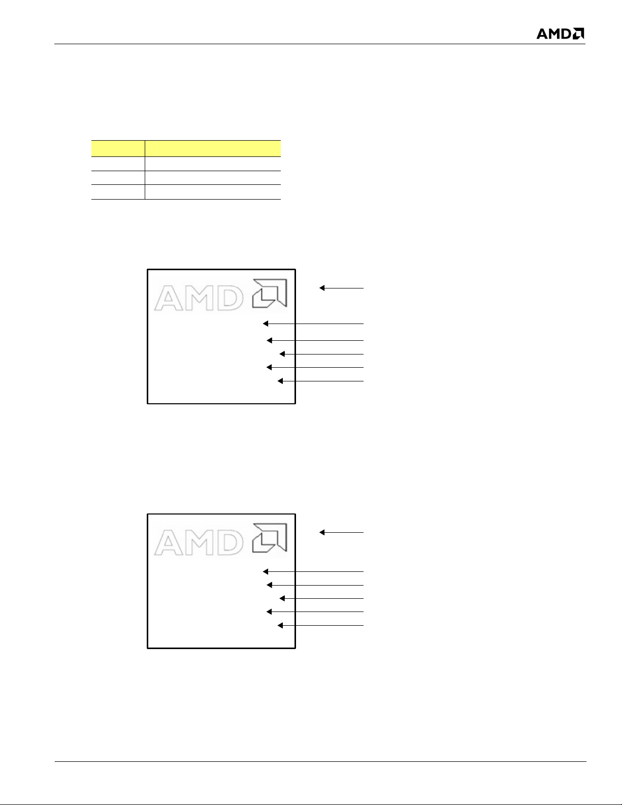
Device ID
Northbridge
YYWW
MADE IN TAIWAN
WXXXXX
215-0716032
* YY - Assembly Start Year
WW - Assembly Start Week
Part Number
Date Code*
AMD Product Type
AMD Logo
Wafer Lot Number
Country of Origin
Note: Branding can be in laser, ink, or
mixed laser-and-ink marking.
Northbridge
YYWW
MADE IN TAIWAN
WXXXXX
215-0716042
* YY - Assembly Start Year
WW - Assembly Start Week
Part Number
Date Code*
AMD Product Type
AMD Logo
Wafer Lot Number
Country of Origin
Note: Branding can be in laser, ink, or
mixed laser-and-ink marking.
1.4 Device ID
The SR5650 is a member of the AMD chipset family, which consists of different devices designed to support different
platforms. Each device is identified by a device ID, which is stored in the NB_DEVICE_ID register. The device IDs for
the SR5650/5690/5670 chipset family are as follows:
Table 1-1 Device IDs for the SR5690/5670/5650 Chipset Family
Device Device ID
SR5690 5A10h
SR5670 5A12h
SR5650 5A13h
1.5 Branding Diagrams
© 2011 Advanced Micro Devices, Inc. 47062 SR5650 Databook 2.10
Proprietary 1-3
Figure 1-1 SR5650 Branding Diagram for A21 Production ASIC (Eutectic Part)
Figure 1-2 SR5650 Branding Diagram for A21 Production ASIC (Lead Free Part)
Page 14
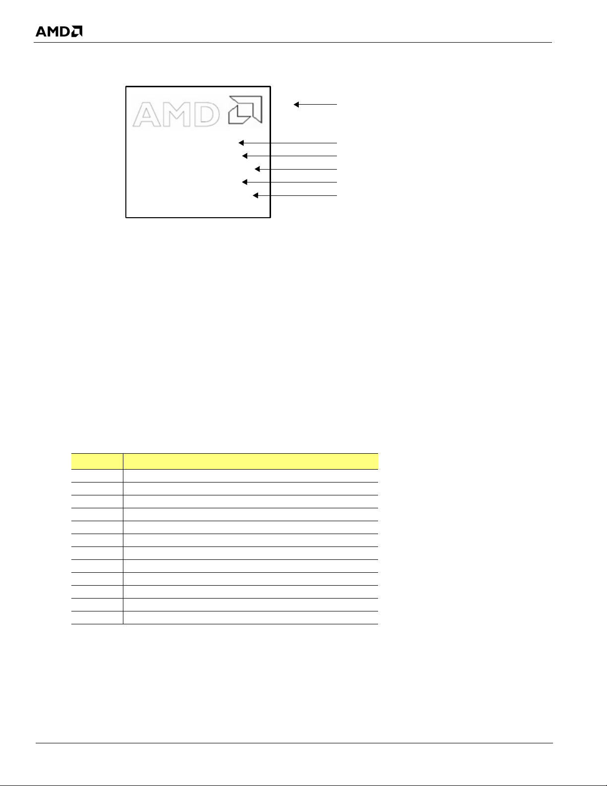
Northbridge
YYWW
MADE IN TAIWAN
WXXXXX
215-0716054
* YY - Assembly Start Year
WW - Assembly Start Week
Part Number
Date Code*
AMD Product Type
AMD Logo
Wafer Lot Number
Country of Origin
Note: Branding can be in laser, ink, or
mixed laser-and-ink marking.
Figure 1-3 SR5650 Alternate Branding for A21 Production ASIC (Lead Free Part)
1.6 Conventions and Notations
Conventions and Notations
The following sections explain the conventions used throughout this manual.
1.6.1 Pin Names
Pins are identified by their pin names or ball references. All active-low signals are identified by the suffix ‘#’ in their
names (e.g., SYSRESET#).
1.6.2 Pin Types
The pins are assigned different codes according to their operational characteristics. These codes are listed in Table 1-2.
Table 1-2 Pin Type Codes
Code Pin Type
I Digital Input
O Digital Output
I/O Bi-Directional Digital Input or Output
M Multifunctional
Pwr Power
Gnd Ground
A-O Analog Output
A-I Analog Input
A-I/O Analog Bi-Directional Input/Output
A-Pwr Analog Power
A-Gnd Analog Ground
Other Pin types not included in any of the categories above
1.6.3 Numeric Representation
Hexadecimal numbers are appended with “h” whenever there is a risk of ambiguity. Other numbers are in decimal.
Pins of identical functions but different trailing digits (e.g., DFT_GPIO0, DFT_GPIO1, ...DFT_GPIO5) are referred to
collectively by specifying their digits in square brackets and with colons (i.e., “DFT_GPIO[5:0]”). A similar short-hand
notation is used to indicate bit occupation in a register. For example, NB_COMMAND[15:10] refers to the bit positions
10 through 15 of the NB_COMMAND register.
47062 SR5650 Databook 2.10 © 2011 Advanced Micro Devices, Inc.
1-4 Proprietary
Page 15
Conventions and Notations
1.6.4 Hyperlinks
Phrases or sentences in blue italic font are hyperlinks to other parts of the manual. Users of the PDF version of this manual
can click on the links to go directly to the referenced sections, tables, or figures.
1.6.5 Acronyms and Abbreviations
The following is a list of the acronyms and abbreviations used in this manual.
Table 1-3 Acronyms and Abbreviations
Acronym Full Expression
ACPI Advanced Configuration and Power Interface
ASPM Active State Power Management
A-Link-E A-Link Express interface between the Northbridge and Southbridge.
BGA Ball Grid Array
BIOS
BIST Built In Self Test.
DBI Dynamic Bus Inversion
DPM Defects per Million
EPROM Erasable Programmable Read Only Memory
FCBGA Flip Chip Ball Grid Array
FIFO First In, First Out
VSS Ground
GPIO General Purpose Input/Output
HT HyperTransport™ interface
IDDQ Direct Drain Quiescent Current
IOMMU Input/Output Memory Management Unit
JTAG Joint Test Access Group. An IEEE standard.
MB Mega Byte
NB Northbridge
PCI Peripheral Component Interface
®
PCIe
PLL Phase Locked Loop
POST Power On Self Test
PD Pull-down Resistor
PU Pull-up Resistor
RAS Reliability, Availability and Serviceability
SB Southbridge
TBA To Be Added
VRM Voltage Regulation Module
Basic Input Output System. Initialization code stored in a ROM or Flash RAM used to start up a
system or expansion card.
PCI Express
®
© 2011 Advanced Micro Devices, Inc. 47062 SR5650 Databook 2.10
Proprietary 1-5
Page 16

This page is left blank intentionally.
Conventions and Notations
47062 SR5650 Databook 2.10 © 2011 Advanced Micro Devices, Inc.
1-6 Proprietary
Page 17
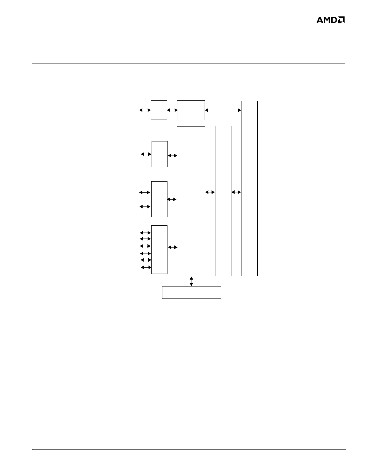
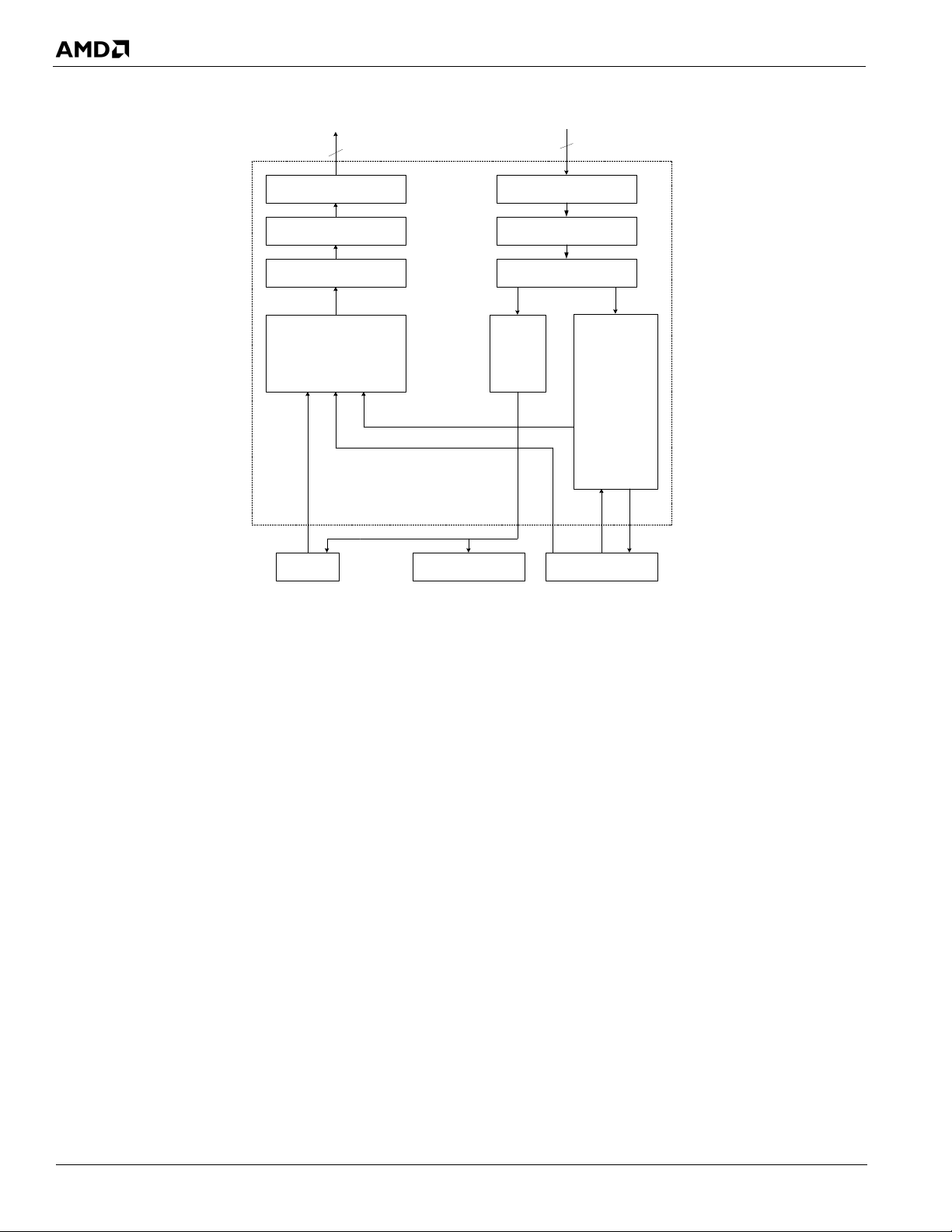
Chapter 2
HyperTransport™ 3
Unit
CPU
Interface
Root
CPU
Southbridge
Complex
A-Link-E
Interface
GPP3 Interface
PCIe
(6 Lanes for 6 ports)
Expansion
Slots
(1 x 4 Lanes)
IO Controller
GPP1 Interface
PCIe
®
Register Interface
(1 x 16 or 2 x 8 Lanes)
IOMMU
Expansion
Slots
Functional Descriptions
This chapter describes the functional operation of the major interfaces of the SR5650 system logic chip. Figure 2-1
illustrates the SR5650 internal blocks and interfaces.
Figure 2-1 SR5650 Internal Blocks and Interfaces
2.1 HyperTransport™ Interface
2.1.1 Overview
The SR5650 is optimized to interface with “Shanghai” and subsequent series of AMD server/workstation and desktop
processors through sockets F, AM3, G34, and C32. The SR5650 supports HyperTransport
HyperTransport 1 (HT1) for backward compatibility and for initial boot-up. For a detailed description of the interface,
please refer to the HyperTransport I/O Link Specification from the HyperTransport Consortium. Figure 2-2,
“HyperTransport™ Interface Block Diagram,” illustrates the basic blocks of the host bus interface of the SR5650.
™
3 (HT3), as well as
© 2011 Advanced Micro Devices, Inc. 47062 SR5650 Databook 2.10
Proprietary 2-1
Page 18
I/O Controller
Upstream Arbitration
IOMMU L2
10.4 GB/s to
CPU
Response
Interface
Host Interface
Host
requests
Host read
responses
Host read
responses
DMA requests
DMA
read
response
data
IOMMU
requests
10.4 GB/s from
CPU
Rx PHYTx PHY
Rx PHY InterfaceTx PHY Interface
Protocol ReceiverProtocol Transmitter
PCIe® Cores
HyperTransport™ Interface
Figure 2-2 HyperTransport™ Interface Block Diagram
The SR5650 HyperTransport bus interface consists of 16 unidirectional differential Command/Address/Data pins, and 2
differential Control pins and 2 differential Clock pins in both the upstream and downstream directions. On power up, the
link is 8-bit wide and runs at a default speed of 400MT/s in HyperTransport 1 mode. After negotiation, carried out by the
HW and SW together, the link width can be brought up to the full 16-bit width and the interface can run up to 5.2GT/s in
HyperTransport 3 mode. In HyperTransport 1 mode, the interface operates by clock-forwarding while in HyperTransport
3 mode, the interface operates by dynamic phase recovery, with frequency information propagated over the clock pins.
The interface is illustrated below in Figure 2-3, “SR5650 HyperTransport™ Interface Signals.” The signal name and
direction for each signal is shown with respect to the SR5650. Detailed descriptions of the signals are given in Section 3.3,
“CPU HyperTransport™ Interface‚’ on page 3-4.
47062 SR5650 Databook 2.10 © 2011 Advanced Micro Devices, Inc.
2-2 Proprietary
Page 19
HyperTransport™ Interface
HT_TXCALP
HT_RXCALN
HT_RXCALP
HT_TXCALN
HT_RXCADN
2
2
SR5650
CPU
HT_RXCADP
HT_RXCTLN
HT_RXCTLP
HT_RXCLKN
HT_RXCLKP
16
16
HT_TXCADN
2
2
HT_TXCADP
HT_TXCTLN
HT_TXCTLP
HT_TXCLKN
HT_TXCLKP
16
16
2
2
2
2
2.1.2 HyperTransport™ Flow Control Buffers
Figure 2-3 SR5650 HyperTransport™ Interface Signals
The SR5650 HyperTransport interface has the following features:
• HyperTransport 3.0 compliant
• 16-bit and 8-bit link widths supported. Width for each direction of the link is independently controlled.
• 400MT/s to 5.2GT/s link speeds in increments of 400MT/s (up to 2GT/s only for HyperTransport 1 mode)
• DC-coupled HyperTransport mode only
• UnitID clumping for x16 PCI Express
®
ports
• Isochronous flow-control mode for Southbridge audio and IOMMU traffic
• 64-bit address extension support (52-bit physical addressing)
• Link disconnection with tristate, LS1, and LS2 low-power modes
• Error retry in HyperTransport 3 mode
• Full HyperTransport-defined BIST support for both internal and external loopback modes
The SR5650 HTIU implements the following flow control buffers in its receiver:
Table 2-1 SR5650 HyperTransport™ Flow Control Buffers
Flow Control Buffer Type Posted Non-Posted Response
Cmd 16 16 Advertise 63 credits.
Data 16 1 Advertise 63 credits.
ISOC Cmd 0 0 Advertise 63 credits.
ISOC Data 0 0 Advertise 63 credits.
© 2011 Advanced Micro Devices, Inc. 47062 SR5650 Databook 2.10
Proprietary 2-3
Page 20

2.2 IOMMU
The SR5650’s IOMMU (Input/Output Memory Management Unit) block provides address translation and protection
services as described in version 1.26 of the AMD I/O Virtualization Technology (IOMMU) Specification. The SR5650
also supports the PCI Express Address Translation Services 1.0 Specification, which allows the supporting of endpoint
devices to request and cache address translations.
When DMA requests containing virtual addresses are received, the IOMMU looks up the page translation tables located
in the system memory in order to convert the virtual addresses into physical addresses and to verify access privileges.
On-chip caching is provided in order to speed up translation and reduce or eliminate the number of system memory
accesses required. Every PCIe core contains a local translation cache, and the SR5650 also contains a shared global
translation cache.
The SR5650 supports up to 2
52-bit physical address space.
16
domains, each of which can utilize a separate 64-bit virtual address space. It supports a
2.3 Multiple Northbridge Support
Multiple SR5690/5670/5650 (referred to as “SR56x0”below) Northbridges may be implemented in the same system given
enough free HyperTransport links from the processor complex. However, only a single Southbridge may be used. The
SR56x0 attached to the Southbridge is called the primary SR56x0, and any other instance of SR56x0 is called a secondary
SR56x0. The A-Link Express interface on any secondary SR56x0 must be left unconnected, and it cannot be used to
support any PCI Express endpoint devices.
IOMMU
The PWM_GPIO5 pin-strap is used to indicate whether an SR56x0 is a primary or a secondary Northbridge. If no
pull-down resistor is attached on the pin, the internal pull-up resistor on it will set the strap value to “1,” indicating the
device to be a primary Northbridge. On any secondary SR56x0, the PWM_GPIO5 pin-strap must be pulled low.
In the multi-NB mode, special PCI Express messages for functions such as PME may be passed from a secondary SR56x0
to the primary SR56x0 or the Southbridge over the HyperTransport bus. If the SR56x0’s internal IOAPIC is not used,
INTx messages may also be forwarded over the HyperTransport bus to the Southbridge IOAPIC. Peer-to-peer writes
between PCI Express endpoints are also allowed between any SR56x0 and another by routing peer-to-peer requests over
the HyperTransport bus.
Note: As it is possible to mix-and-match SR5650, SR5670, and SR5690 on the same system, whenever a
multiple-SR5650 configuration is being referred to in this document, it actually represents any combination of SR5650,
SR5670, and SR5690 possible under that situation. Some constrains may apply.
2.4 Interrupt Handling
2.4.1 Legacy INTx Handling
In legacy interrupt mode, all INTx messages must be routed to the Southbridge IOAPIC. The primary NB directs all INTx
messages directly down to the Southbridge IOAPIC. Secondary NBs direct INTx messages up to the processor complex,
where they are broadcast down to all HT devices. See Section 2.3, “Multiple Northbridge Support‚’ on page 2-4 for
details.
The 4 legacy interrupts sent by endpoint devices (INT A/B/C/D) may undergo a 2-stage programmable swizzling process
that maps them onto the 8 possible internal INTx messages (INT A/B/C/D/E/F/G/H). The first swizzling stage is
performed by rotating the interrupt message number based upon the bridge device number. The second stage is register
controllable on a per-bridge basis and maps the rotated INT A/B/C/D onto INT E/F/G/H. INT A to H messages sent to the
Southbridge are mapped onto the SB IOAPIC interrupt redirection table entries 16 to 23.
2.4.2 Non-SB IOAPIC Support
The SR5650 supports routing legacy IOAPIC memory-mapped I/O addresses (0xFECx_xxxx) to any PCI Express port to
support endpoint devices with integrated IOAPIC.
47062 SR5650 Databook 2.10 © 2011 Advanced Micro Devices, Inc.
2-4 Proprietary
Page 21

Interrupt Handling
2.4.3 Integrated IOAPIC Support
The SR5650 supports routing local INTx messages to its integrated IOAPIC. The integrated IOAPIC contains a 32-entry
redirection table. INTx messages from endpoint devices, bridges, HTIU, and IOMMU can be mapped onto different
redirection entries under register control.
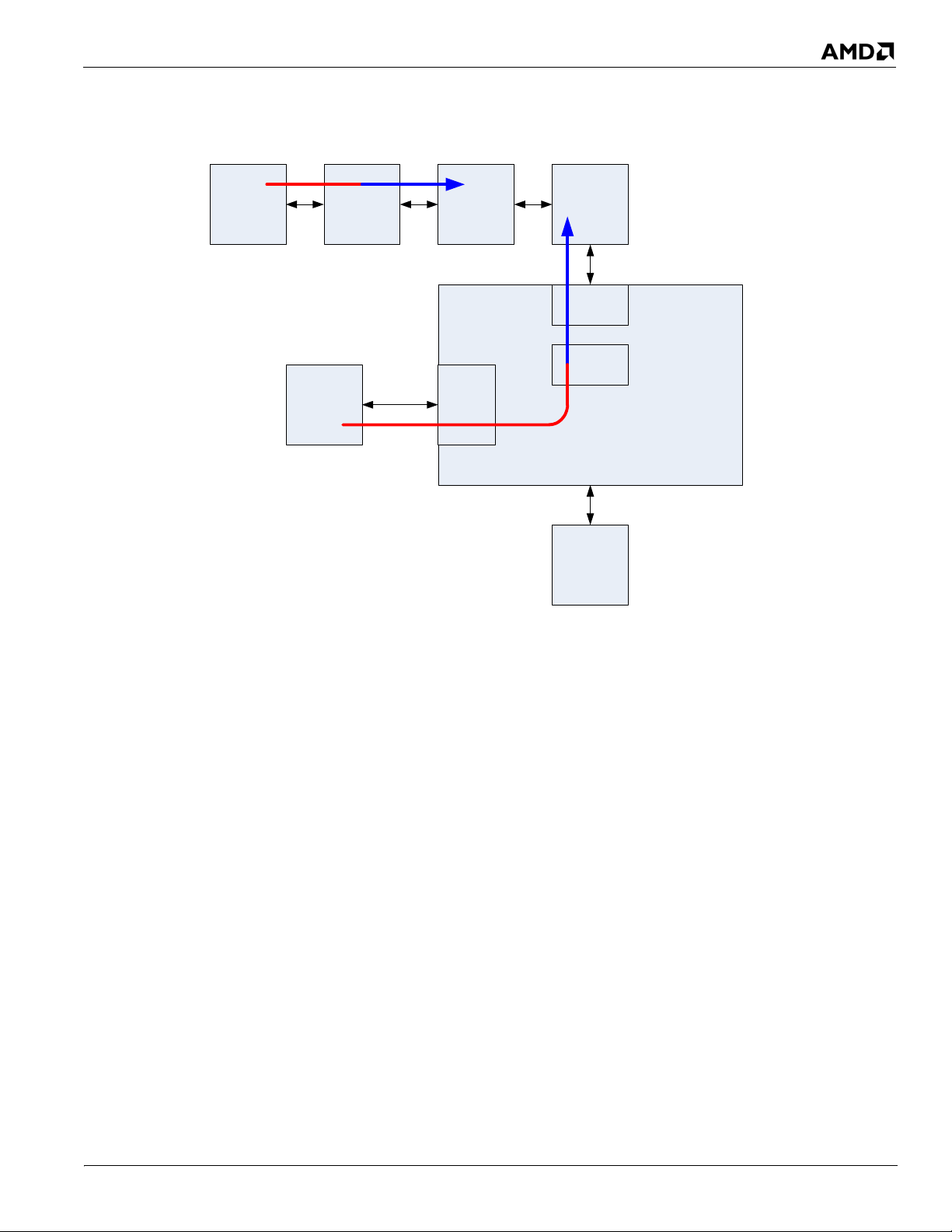
2.4.4 MSI Interrupt Handling and MSI to HT Interrupt Conversion
In MSI interrupt mode, all interrupts are sent directly from the endpoint devices through the SR5650 up to the processor
complex. All MSI interrupts are converted into HT-formatted interrupts. For MSIs from PCI Express endpoint devices
and internally generated PCI Express interrupts, the conversion occurs in the associated IOMMU L1 block. For IOMMU
interrupts and, optionally, HT error interrupts and internal parity error interrupts, the conversion occurs in the HTIU
block. HT error interrupts and internal parity error interrupts may be optionally redirected to an MSI generation block
underneath the SB VC1 IOMMU L1 so that they can be remapped by IOMMU. IOMMU internal MSI interrupts are never
remapped.
The PCI configuration spaces of each on-board device contains a fixed HT MSI mapping capability (except for Device 1,
which is unused). This implies that all MSI interrupts with address 0xFEEx_xxxx have to be converted to HT interrupts.
Because of this, software is required to program all MSI address registers with an 0xFEEx_xxxx address.
2.4.5 Internally Generated Interrupts
The SR5650 may internally generate interrupts for the following purposes:
• PCI Express error
• PCI Express PME
• HT error
• Internal parity error
• IOMMU command handler
• IOMMU event logger
Internally generated interrupts may be in either legacy INTx or MSI format. Internal MSI interrupt sources do not support
per-vector masking.
2.4.6 IOMMU Interrupt Remapping
When the IOMMU is enabled, interrupts generated downstream of the IOMMU are remapped based upon the IOMMU
tables. The following classes of interrupts are not remapped by the IOMMU because they are generated upstream of the
IOMMU:
• HT error (optional)
• Internal parity error (optional)
• IOMMU command handler and event logger
2.4.7 Interrupt Routing Architecture
2.4.7.1 Legacy Mode
Primary SR5650: Legacy INTx messages are routed directly to the SB IOAPIC. The SB IOAPIC generates upstream
interrupt requests, which are translated by the IOMMU before they are delivered up to the processor complex.
Secondary SR5650: Legacy INTx messages are routed over HyperTransport through the processor complex to the
primary SR5650, which forwards them to the SB IOAPIC. The SB IOAPIC generates upstream interrupt requests, which
are translated by the IOMMU before being delivered up to the processor complex.
The routing paths are illustrated in Figure 2-4 below.
© 2011 Advanced Micro Devices, Inc. 47062 SR5650 Databook 2.10
Proprietary 2-5
Page 22
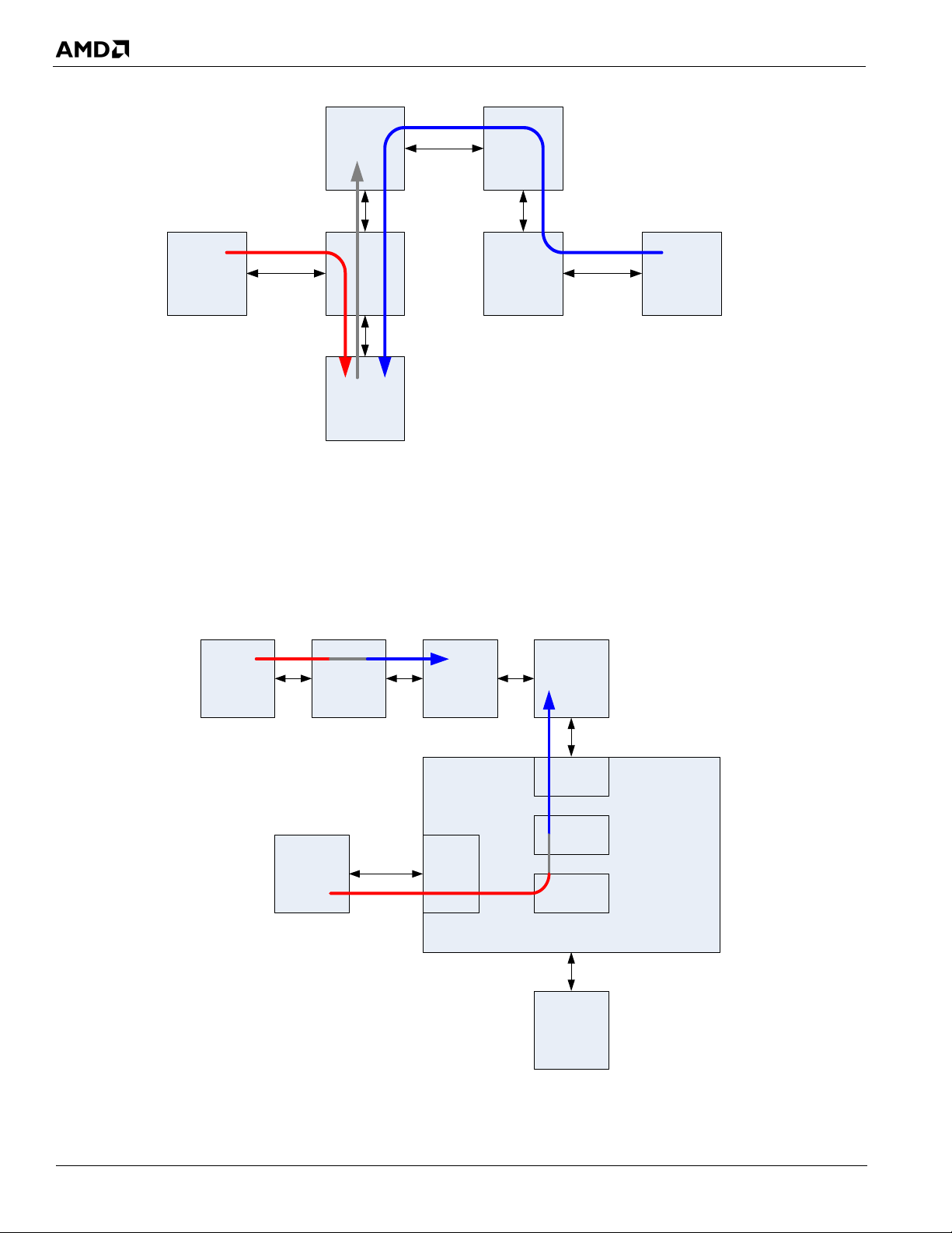
Interrupt Handling
CPU
SR5650
CPU
SR5650
SB
PCI-E
Endpoint
Device
PCI-E
Endpoint
Device
INTx Message from device attached to primary SR5650
INTx Message from device attached to secondary SR5650
Interrupts from SB IOAPIC
CPU
SB
PCI-E
Endpoint
Device
IOMMU
HT
PCI-
Express
IOAPIC
SR5650
INTx Message from PCI-Express device attached to SR5650
Internal interrupt
Remapped HT Interrupt
SR5650
PCI-E
Endpoint
Device
CPU
Figure 2-4 Interrupt Routing Paths in Legacy Mode
2.4.7.2 Legacy Mode with Integrated IOAPIC
For both the primary and secondary SR5650s, legacy INTx messages are routed to the integrated IOAPICs of the
SR5650s, which generates interrupt requests. These requests are remapped by the IOMMU before being delivered up to
the processor complex. If an INTx message gets directed to an IOAPIC table entry that is not enabled, the IOAPIC sends
the INTx message back to the IOC to go to the SB PIC/IOAPIC.
The routing paths are illustrated in Figure 2-5 below.
Figure 2-5 Interrupt Routing Paths in Legacy Mode with Integrated IOAPIC
47062 SR5650 Databook 2.10 © 2011 Advanced Micro Devices, Inc.
2-6 Proprietary
Page 23
RAS Features
CPU
SB
PCI-E
Endpoint
Device
IOMMU
HT
PCI-
Express
SR5650
MSI Interrupt from PCI-Express device attached to SR5650
Remapped HT Interrupt
SR5650
PCI-E
Endpoint
Device
CPU
2.4.7.3 MSI Mode
For both the primary and secondary SR5650s: MSI interrupt requests are remapped by the IOMMU and sent up to the
processor complex. The routing path is illustrated in Figure 2-6 below.
2.5 RAS Features
2.5.1 Parity Protection
All memories in SR5650 are parity protected to reduce the possibility of silent data corruption. Multiple parity words are
interleaved to convert burst errors (multiple physically adjacent bits corrupted) into multiple single-bit detectable errors to
increase robustness. The minimum number of interleaved parity words in any on-board memory is 4. All macros contain
2.5.1.1 Parity Protection for IOMMU Cache Memories
2.5.1.2 Parity Protection for Normal Memories
2.5.2 SERR_FATAL# and NON_FATAL_CORR# Pins
© 2011 Advanced Micro Devices, Inc. 47062 SR5650 Databook 2.10
Proprietary 2-7
test circuitry for software to generate false errors on either the read or write side of the memory for verification of error
handling routines. Error injection circuitry only corrupts parity bits rather than real data bits to avoid data corruption.
All IOMMU cache memories are parity protected. When a parity error is detected, the access from the associated bank is
marked as an automatic miss. The cache line is marked as invalid and may later be overwritten with data from system
memory (which is ECC protected). The error is logged in a status bit and an optional interrupt is generated (either fatal,
non-fatal, or correctable parity error).
All normal memories are also parity protected. When a parity error is detected, the failure is likely to be fatal as there is no
automatic recovery mechanism and no way for hardware to tag a specific request or operation with the error. The error is
logged in a status bit for later diagnosis and an optional interrupt is generated (either fatal or non-fatal parity error).
The SR5650 implements a dedicated pin, DBG_GPIO0/SERR_FATAL#, to signal either a system or a fatal error, which
can be used to signal a BMC for further actions. SERR_FATAL# may be asserted on various error conditions like HT
Figure 2-6 Interrupt Routing Path in MSI Mode
Page 24

syncflood, as well as internal parity errors or fatal errors for which signalling by SERR_FATAL# is enabled. Fatal errors
are identified via the fatal error status bits.
Non-fatal or correctable errors may be likewise signalled via DBG_GPIO3/NON_FATAL_CORR#.
The SERR_FATAL# and NON_FATAL_CORR# pin functionalities are disabled on warm reset.
2.5.3 NMI# and SYNCFLOODIN#
The SR5650 may configure the DFT_GPIO0/NMI# pin as an input pin for triggering an upstream NMI packet to the
processor complex. The pin should be driven by a BMC. An internal sticky status bit records the use of the NMI# pin.
Also, the SR5650 may configure the DFT_GPIO5/SYNCFLOODIN# pin as an input pin for triggering a HyperTransport
syncflood event. The pin should driven by a BMC. An internal sticky status bit records the use of the SYNCFLOODIN#
pin.
2.5.4 Suggested Platform Level RAS Sideband Signal Connections
Figure 2-7 is a logical diagram showing suggestions for RAS sideband signal connections at the platform level .
RAS Features
47062 SR5650 Databook 2.10 © 2011 Advanced Micro Devices, Inc.
2-8 Proprietary
Page 25

RAS Features
SR5650
BMC, SuperIO or other GPIO
source
SP5100
DBG_GPIO0/
SERR_FATAL#
DBG_GPIO3/
NON_FATAL_CORR#
Attach to a pin that can
generate SMI# like
USB_OC5#/IR_TX0/
GPM5#
DFT_GPIO0/NMI#
DFT_GPIO5/
SYNCFLOODIN#
Enable only after
reset. This is a pin-
strap sampled
shortly after
powergood
Enable signals
should default to
logic 0 on reset/
powergood
Add option to drive
SYNCFLOODIN#
pins on all SR5650s
in the system
SERR_FATAL# and
NON_FATAL_CORR#
from other SR5650s.
These are buffered to help
isolate the failing device.
S/W path to
trigger NMI#
pin
Enable only after
reset. This is a pin-
strap sampled
shortly after
powergood
PCIe
®
From NMI button and
MCARD_NMIBTN_L
OPMA pin
To
SYS_NMIBTN_L
OPMA pin
GPIO Expander
attached to OPMA
SMBus (either private
0 or private 1 SMBus
segments).
Alternately, this can
connect directly to a
BMC
SCL/SDA
Interrupt l ine to
Sys_SMBUS_IO_EXP_INTR_L
OPMA pin
Separate connections to
debug pins and GPIO
expander for each SR5650
in the system
NMI# only needs to
be connected on
the primary SR5650
Figure 2-7 Suggested Platform Level RAS Sideband Signal Connections
2.5.5 Error Reporting and Logging
2.5.5.1 PCI Error Logging
The SR5650 implements all PCI standard error logging bits for all on-board devices and functions including the host
bridge device, IOMMU, and PCI Express bridges.
2.5.5.2 PCIe
The SR5650 PCIe
®
Advanced Error Reporting
®
cores implement the optional Advanced Error Reporting (AER) feature mechanism in the PCI
Express 2.0 Base Specification. Errors are logged for received packet errors such as poisoned data, malformed TLP, and
etc. within the PCIe core and are accessible via the bridge configuration spaces.
© 2011 Advanced Micro Devices, Inc. 47062 SR5650 Databook 2.10
Proprietary 2-9
Page 26
RAS Features
The ACS violations for ACS Source Validation and ACS Translation Blocking are recorded in the AER error log. Errors
due to IOMMU translation failures are not logged as ACS violations, but are logged as UR or CA depending on the error
type.
IOC may abort a non-posted request with UR status if it determines that the request will not hit system memory. Such
errors are pushed back into the PCIe core for logging. The IOC must abort potential peer-to-peer non-posted requests to
avoid a deadlock condition. For posted requests, the IOC can be configured to forward all non-decoded (non system
memory and non-peer-to-peer) posted requests up to the processor, which may abort the request and generate an MCA
error log.
For downstream completions with abort status coming back from the processor, error status is propagated to the endpoint
but no AER header information is logged in the chipset.
For upstream completions, error status is propagated up to the processor and AER information may be logged.
Table 2-2 lists the types of errors that are detectable by the SR5650 AER implementation. For details, see the PCI Express
2.0 Base Specification.
Table 2-2 Types of Errors Detectable by the SR5650 AER Implementation
Error Type Error Class
ACS Violation Uncorrectable – Fatal or Non-fatal
Unsupported Request Uncorrectable – Fatal or Non-fatal
Malformed TLP Uncorrectable – Fatal or Non-fatal
Unexpected Completion Uncorrectable – Fatal or Non-fatal
Completer Abort Uncorrectable – Fatal or Non-fatal
Completion Timeout Uncorrectable – Fatal or Non-fatal
Poisoned TLP Received Uncorrectable – Fatal or Non-fatal
Data Link Layer Protocol Error Uncorrectable – Fatal or Non-fatal
ECRC Error Uncorrectable – Fatal or Non-fatal
Replay Timeout Correctable
REPLAY_NUM Rollover Correctable
Bad DLLP Correctable
Bad TLP Correctable
The following error classes are NOT supported:
• Receiver Overflow Error
• Flow Control Error
• Surprise Down Error
• Receiver Error
2.5.5.3 IOMMU Error Reporting
The IOMMU specification defines a standard error logging facility that logs error events in system memory with register
status bits or interrupt notification to system software. The SR5650 fully supports the generation of logging events
following this standard.
2.5.5.4 HyperTransport™ Error Reporting
The HyperTransport specification defines various levels of error handling for link-related errors. The SR5650 supports
the detection of most error classes including protocol error, overflow error, and response error. The SR5650 also supports
notification of error conditions via fatal interrupts, non-fatal interrupts, or syncflood.
Table 2-3 lists the types of errors supported by the error handling capabilities of the SR5650 for HyperTransport.
47062 SR5650 Databook 2.10 © 2011 Advanced Micro Devices, Inc.
2-10 Proprietary
Page 27
RAS Features
Table 2-3 Types of HyperTransport™ Errors Supported by the SR5650
Error Type Description
Response Error Received incorrect response type such as tgtdone for read request, read response for flush, or size of
Overflow Error Flow-control buffer overflow in the receiver. This is only mapped to a fatal or non-fatal error in HT1
CRC Error Periodic CRC error
Retry Error Per-packet CRC error received
Retry Count Rollover Per-packet CRC error counter overflowed. Non-fatal interrupt only.
Protocol Error Protocol conditions detected in HT1 mode:
received data did not match size of requested data.
mode. In HT3 mode, this maps onto a retry in the hope that when the packet is subsequently received,
there is space in the FCB. No interrupt will be generated in HT3 mode.
• Data count not matching header
• Invalid command encoding
• Invalid CTL encoding
• Incomplete header
• Unexpected data
Protocol conditions detected in HT3 mode
• Data count not matching header
• Invalid command encoding
• Invalid CTL encoding
• Incomplete header
• Unexpected data
• Unexpected CRC
• Missing CRC
• Non-NOP inserted command
• Inserted command without inserted command CTL encoding
End of chain error is not supported, since the end of the chain is on PCI Express instead HyperTransport.
2.5.5.5 Internal Parity Error Reporting
One register bit per memory macro is used to log parity errors. Values for those bits are persistent across a warm reset for
diagnostic purposes.
2.5.6 Interrupt Generation on Errors
Internal interrupts may be generated on the following error conditions:
• PCI Express errors (fatal, non-fatal, or correctable)
• HT errors (fatal or non-fatal)
• IOMMU events
• Internal parity error (fatal or non-fatal)
• Internal parity error in the IOMMU cache (fatal, non-fatal, or correctable)
2.5.7 Poisoned Data Support
The SR5650 supports the propagation of poisoned data attributes (EP in PCIe and Data Error in HT) between PCI Express
endpoints and the processor for both host and DMA requests or responses. The SR5650 cannot actively mark a transaction
with a poisoned data attribute even if the transaction encounters an internal parity error. Received packets containing
ECRC errors are not marked as poisoned.
2.5.8 PCIe® Link Disable State
The SR5650 has the ability to put PCIe links into the disabled state as an error response in order to help stop data
movement within the system. Links which received fatal errors may be disabled. Also, a HyperTransport syncflood event
may be used to trigger all links to enter the disabled state.
© 2011 Advanced Micro Devices, Inc. 47062 SR5650 Databook 2.10
Proprietary 2-11
Page 28

2.5.9 HT Syncflood Based on PCIe® Error
The SR5650 has the ability to put the HyperTransport link into the syncflood state when a fatal or non-fatal error is
received on the PCIe interface. This is done in order to help stop data movement within the system.
PCI
Express®
2.6 PCI Express
2.6.1 PCIe® Ports
In total, there are 9 PCIe® ports on the SR5650, divided into 3 groups and implemented in hardware as 3 separate cores:
• PCIE-GPP1: 2 general purpose ports, 16 lanes in total. Width of each port is x8. In the default configuration, the 2
ports are combined to provide a 1 x16 port.
• PCIE-GPP3: 6 general purpose ports, with 6 lanes in total. They support 6 different configurations with respect to
link widths: 4:2, 4:1:1, 2:2:2, 2:2:1:1, 2:1:1:1:1, and 1:1:1:1:1:1 (default configuration). For details on the possible
configurations for the GPP3 lanes, see Table 2-4 below and .
Table 2-4 Possible Configurations for the PCI Express® General Purpose Links
PCIe Core Physical Lane Config. B Config. C Config. C2 Config. E Config. K Config. L
GPP3
• PCIE-SB: The Southbridge port provides a dedicated x4 link to the Southbridge (also referred to as the “A-Link
Express II interface”).
Each port supports the following PCIe functions:
®
GPP3 lane 0
GPP3 lane 1 x1
GPP3 lane 2
GPP3 lane 3 x1 x1
GPP3 lane 4
GPP3 lane 5 x1 x1 x1 x1
x4 x4
x2
x1
x2 x2 x2
x2
x2
x1
x1 x1 x1
x2
x1
x1
• PCIe Gen 1 link speeds
• ASPM L0s and L1 states
• ACPI power management
• Endpoint and root complex initiated dynamic link degradation
• Lane reversal
• Alternative Routing-ID Interpretation (ARI)
• Access Control Services (ACS)
• Advanced Error Reporting (AER)
• Address Translation Services (ATS)
2.6.2 PCIe® Reset Signals
Reset signals to PCIe slots, as well as embedded PCIe devices, must be controlled through one or more
software-controllable GPIO pins instead of the global system reset. It is recommended that unique GPIO pins be used for
each slot or device. The SR5650 has four GPIO pins that may be used for the purpose of driving reset signals
(PCIE_GPIO_RESET[5:4] and PCIE_GPIO_RESET[2:1]). Additional reset GPIO pins may be driven by
platform-specific means such as a super I/O or an I/O expander.
2.7 External Clock Chip
On the SR5650 platform, an external clock chip provides the CPU, PCI Express, and A-Link Express II reference clocks.
For requirements on the clock chip, please refer to the 800-Series IGP Express AMD Platform External Clock Generator
Requirements Specification for Server Platforms.
47062 SR5650 Databook 2.10 © 2011 Advanced Micro Devices, Inc.
2-12 Proprietary
Page 29

Chapter 3
Pin Descriptions and Strap Options
This chapter gives the pin descriptions and the strap options for the SR5650. To jump to a topic of interest, use the
following list of hyperlinked cross references:
“Pin Assignment Top View” on page 3-2
“SR5650 Interface Block Diagram” on page 3-4
“CPU HyperTransport™ Interface” on page 3-4
“PCI Express® Interfaces” on page 3-5:
“PCI Express® Interface for General Purpose External Devices” on page 3-5
“A-Link Express II Interface to Southbridge” on page 3-5
“Miscellaneous PCI Express® Signals” on page 3-6
“Clock Interface” on page 3-6
“Power Management Pins” on page 3-6
“Miscellaneous Pins” on page 3-7
“Power Pins” on page 3-7
“Ground Pins” on page 3-9
“Strapping Options” on page 3-10
© 2011 Advanced Micro Devices, Inc. 47062 SR5650 Databook 2.10
Proprietary 3-1
Page 30
3.1 Pin Assignment Top View
1234567891011121314
A
B
C
VDDPCIE VSS VDDPCIE VSS GPP1_RX6N VSS GPP1_TX4N VSS GPP1_TX2N VSS GPP1_TX0N VDDA18PCIE VDDA18PCIE VSS
D
GPP1_RX7N GPP1_RX 7P VSS VDDPCIE VSS GPP1_RX5P VSS GP P1_RX3P VSS G PP1_RX1P VSS VDDA18PCIE VDDA18P CIE VSS
E
F
GPP1_TX8N GPP1_TX8P VSS GPP1_RX8N GPP1_RX8P VDDPCIE GPP1_RX4N VSS GPP1_RX2N VSS GPP1_RX0N VDDA18PCIE VDDA18PCIE PCE_TCALRP
G
H
GPP1_TX10N GPP1_TX10P VSS GPP1_RX10N GPP1_RX10P VSS VDDPCIE
J
GPP1_TX12N GPP1_TX12P VSS GPP1_RX12N GPP1_RX12P VSS VDDPCIE VSS
K
L
M
GPP1_TX14N GPP1_TX14P VSS GPP1_RX14N GPP1_RX14P VSS VDDPCIE VSS VSS VSS VDDC VS S
N
PNCNC
R
TNCNC
U
VNCNC
W
YNCNC
AA
AB NC NC
AC
AD NC NC
AE
AF NC NC
AG
AH
VDDPCIE VSS GPP1_TX6N GPP1_RX6P GPP1_TX5N GPP1_TX4P GPP1_TX3N GPP1_TX2P GPP1_TX1N GPP1_TX0P VDDA18PCIE VDD A18PCIE VSS
VSS GPP1_TX7N GPP1_TX7P VSS VDDPCIE GPP1_RX5N GPP1_R X4P GPP1_RX3N GP P1_RX2P GPP1_RX1N GPP1_RX0P VDDA18PCIE VDDA18PCIE PCE_TCALRN
VSS GPP1_TX9N GPP1_TX9P VSS GPP1_RX9N GP P1_RX9P VDDPCIE VDDPCIE VSS VDDPCIE VSS VD DA18PCIE VDDA18PCIE V DDA18PCIE
VSS GPP1_TX11N G PP1_TX11P VSS GPP1_RX11N GPP1_RX11P VSS
VSS GPP1_TX13N GPP1_TX13P VSS GPP1_RX13N GPP1_RX13P VSS VDDPCIE VDDA18PCIE VSS VSS VDDC
VSS GPP1_TX15N GPP1_TX15P VSS GPP1_RX15N GPP1_RX15P VSS VDDPCIE VSS VDDC VSS VDDC
VSS NC NC VSS NC NC VSS VDDPCIE VSS VDD C VSS VDDC
VSS NC NC VSS NC NC VSS NC VSS VSS VSS VDDC
VSS NC NC VSS NC NC VSS VDDPCIE
VSS NC NC VSS NC NC VSS VDDPCIE VSS VDDPCIE VSS VDDPCIE VSS
VSS NC NC VSS VSS VDDPCIE NC VSS NC VSS NC VSS NC VSS
VSS NC NC VDDPCIE VSS NC VSS NC VSS PCE_RCALRP VSS NC VSS NC
VDDPCIE VSSNCNCNCNCNCNCNCNCNCNCGPP3_TX5N
1234567891011121314
VDDPCIE GPP1_TX6P VSS GPP1_TX5P VSS GPP1_TX3P VSS GPP1_TX1P VSS VDDA18P CIE VDDA18PCIE VSS
VDDPCIE VSS NC VSS NC VSS NC VSS NC VSS NC VSS
Pin Assignment Top View
GPP1_REFCL
GPP1_REFCL
VSS NC NC VSS VDDPCIE VSS VSS VSS VDDC VSS
VSS NC NC VSS VDDPCIE VSS VSS VSS VDDC VSS
VSS NC NC VSS VDDPCIE NC VDDA18PCIE VSS VSS VSS
VSS NC NC VSS VDDPCIE VSS
VSS NC NC VSS VDDPCIE VSS VDDPCIE VSS VDDPCIE VSS VDDPCIE VSS
VSS VSS VDDPCIE NC NC NC NC PCE_RCALRN NC NC NC NC
VSS NC VSS NC VSS NC VSS NC VSS NC VSS GPP3_TX5P
VDDPCIE VSS VDDPCIE VDDA18PCIE VDDA18PCIE VDDA18PCIE
KN
KP
GPP3_REFCL
KN
CPU Interface
A-Link Express II Interface
Clock Interface
PCIe® GPP1 General Purpose Interface
PCIe GPP3 General Purpose Interface
Power Management Interface
Core Power
PCIe Main I/O Power
PCIe 1.8V I/O Power and PLL Power
GPIO 1.8V I/O Power
HyperTransport™ Interface Power
Grounds
Other
47062 SR5650 Databook 2.10 © 2011 Advanced Micro Devices, Inc.
3-2 Proprietary
Page 31
Pin Assignment Top View
15 16 17 18 19 20 21 22 23 24 25 26 27 28
PWM_GPIO4 VSS
PWM_GPIO2
SYSRESET# VSS
GPP3_REFCL
GPP3_RX5N VSS GPP3_RX3N VSS GPP3_R X1N VSS SB_RX3P VDDHT HT_RXCAD9N HT_RXCAD9P VSS HT_RXCAD1N HT_RXCAD1P VSS AC
GPP3_RX5P GPP3_RX4N GPP3_RX3P GPP3_RX2N GPP3_RX1P PCE_BCALRN SB_RX3N SB_RX2P VDDHT HT_RXCAD8N HT_RXCAD8P VSS HT_RXCAD0N HT_RXCAD0P AD
GPP3_TX4N VSS GPP3_TX2N VSS GPP3_TX0N VSS SB_ TX2P VSS SB_TX1P VSS SB_RX1P VSS VDDHT VSS AF
GPP3_TX4P GPP3_TX3N GPP3_TX2P GPP3_TX1N GPP 3_TX0P GPP3_RX0N SB_TX2N SB_TX3P SB_TX1N SB_TX0P SB_RX1N SB_RX0P VSS AG
PWM_GPIO6 OSCIN VDD18
VSS PWM_GPIO5 VSS VDD18 VSS I2C_DATA VSS
LDTSTOP# PWM_GPIO1
VSS PWM_GPIO3 VSS VSS VSS VSS VSS VDDHTTX VSS HT_TXCAD9P HT_TXCAD9N VSS HT_TXCAD1P HT_TXCAD1N F
VSS VSS VSS VSS VSS VSS
VSS VSS VSS VSS VSS VSS VSS VDDHTTX VSS
VSS VDDC VSS VSS VDDHT VSS
VDDC VSS VSS VSS VSS VDDHT VSS
VSS VDDC VSS VSS VDDHT VSS
VDDC VSS VDDC VSS VSS VDDHT VSS HT_TXCTL1P HT_TXCTL1N VSS HT_TXCTL0P HT_TXCTL0N P
VSS VDDC VSS VSS VDDHT VSS HT_RXCTL1N HT_RXCTL1P VSS HT_RXCTL0N HT_RXCTL0P VSS R
VDDC VSS VDDC VSS VSS VDDHT VSS
VSS VDDC VSS VSS VDDHT VSS
VSS VSS VSS VDDA18PCIE VSS VDDHT VSS
KP
VDDPCIE VSS VDDPCIE VSS VDDPCIE VSS VSS VDDHT VSS
VSS GPP3_RX4P VSS GPP3_RX2P VSS PCE_BCALRP VSS SB_RX2N VSS VDDHT VDDHT VDDHT VDDHT VDDHT AE
VSS GPP 3_TX3P VSS GPP3_TX1P VSS GPP3_RX0P VSS SB_TX3N VSS SB_TX0N VSS SB_RX0N AH
15 16 17 18 19 20 21 22 23 24 25 26 27 28
POWERGOO
PCIE_RESET_
GPIO2
PCIE_RESET_
GPIO5
VDDPCIE VSS VDDPCIE VSS VSS
VDD18 TESTMODE VSS
D
VDD18
VDD18
PCIE_RESET_
GPIO1
PCIE_RESET_
GPIO3
PCIE_RESET_
GPIO4
DBG_GPIO3/
NON_FATAL_CO
I2C_CLK DBG_GPIO2 DBG_GPIO1 DFT_GPIO4 DFT_GPIO2 DFT_GPIO3
VSS
VSS STRP_DATA VDDHTTX HT_TXCAD8P HT_TXCAD8N VSS HT_TXCAD0P HT_TXCAD0N VSS E
RR#
DBG_GPIO0/S
ALLOW_LDTS
VDDA18HTPL
HT_REFCLKN VSS HT_TXCLK1 P HT_TXCLK1N VSS HT_TXCLK0P HT_TXCLK 0N VSS J
HT_REFCLKP VDDHT VSS
THERMALDIO
THERMALDIO
ERR_FATAL#
VDDHTTX VDDHTTX HT_RXCALN HT_RXCALP VSS HT_TXCALN HT_TXCALP D
TOP
VDDHTTX
L
VDDHT VSS
DE_P
DE_N
DFT_GPIO5/
SYNCFLOODIN
VSS
VSS VDDHTTX VDDHTTX VDDHTTX VDDHTTX VDDHTTX C
HT_TXCAD10PHT_TXCAD10
HT_TXCAD13PHT_TXCAD13
HT_TXCAD15PHT_TXCAD15
HT_RXCAD14NHT_RXCAD14
HT_RXCAD12NHT_RXCAD12
VDDHT VSS HT_RX CLK1N HT_RXCLK1P VSS HT_RXCLK0N HT_RXCLK0P Y
HT_RXCAD11NHT_RXCAD11
VDDHT
VSS DFT_GPIO1 VSS A
#
HT_TXCAD11PHT_TXCAD11
HT_TXCAD12PHT_TXCAD12
HT_TXCAD14PHT_TXCAD14
HT_RXCAD15NHT_RXCAD15
HT_RXCAD13NHT_RXCAD13
HT_RXCAD10NHT_RXCAD10
N
N
N
P
P
P
DFT_GPIO0/
NMI#
VSS HT_TXCAD2P HT_TXCAD2N VSS G
VSS HT_TXCAD3P HT_TXCAD3N H
N
VSS HT_TXCAD4P HT_TXCAD4N K
N
VSS HT_TXCAD5P HT_TXCAD5N VSS L
VSS HT_TXCAD6P HT_TXCAD6N M
N
VSS HT_TXCAD7P HT_TXCAD7N VSS N
VSS HT_RXCAD7N HT_RXCAD7P T
P
VSS HT_RXCAD6N HT_RXCAD6P VSS U
VSS HT_RXCAD5N HT_RXCAD5P V
P
VSS HT_RXCAD4N HT_RXCAD4P VSS W
VSS HT_RXCAD3N HT_RXCAD3P VSS AA
VSS HT_RXCAD2N HT_RXCAD2P AB
P
VSS B
CPU Interface
A-Link Express II Interface
Clock Interface
PCIe GPP1 General Purpose Interface
PCIe GPP3 General Purpose Interface
Power Management Interface
Core Power
PCIe Main I/O Power
PCIe 1.8V I/O Power and PLL Power
GPIO 1.8V I/O Power
HyperTransport Interface Power
Grounds
Other
© 2011 Advanced Micro Devices, Inc. 47062 SR5650 Databook 2.10
Proprietary 3-3
Page 32

3.2 SR5650 Interface Block Diagram
HT_RXCAD[15:0]P, HT_RXCAD[15:0]N
HT_RXCLK[1:0]P, HT_RXCLK[1:0]N
HT_RXCTL[1:0]P, HT_RXCTL[1:0]N
HT_TXCTL[1:0]P, HT_TXCTL[1:0]N
HT_RXCALP, HT_RXCALN
HT_TXCALP, HT_TXCALN
HT_TXCLK[1:0]P, HT_TXCLK[1:0]N
HT_TXCAD[15:0]P, HT_TXCAD[15:0]N
SB_TX[3:0]P, SB_TX[3:0]N
SB_RX[3:0]P, SB_RX[3:0]N
OSCIN
SYSRESET#
POWERGOOD
VDDPCIE
VDD18
VDDC
HyperTransport™
Interface
A-Link Express
II Interface
Power
Management
Interface
Clock Interface
VDDHT
VDDA18HTPLL
PCIe® Interface
for General
Purpose
External
Devices
GPP3_TX[5:0]P, GPP3_TX[5:0]N
GPP3_RX[5:0]P, GPP3_RX[5:0]N
PCE_BCALRP, PCE_BCALRN
Misc. PCIe
Signals
HT_REFCLKP, HT_REFCLKN
LDTSTOP#
ALLOW_LDTSTOP
VSS
GPP1_TX[15:0]P, GPP1_TX[15:0]N
GPP1_RX[15:0]P, GPP1_RX[15:0]N
PCIE_RESET_GPIO[5:1]
VDDA18PCIE
GPP3_REFCLKP, GPP3_REFCLKN
GPP1_REFCLKP, GPP1_REFCLKN
PCE_RCALRP, PCE_RCALRN
PCE_TCALRP, PCE_TCALRN
VDDHTTX
TESTMODE
Misc. Signals
I2C_CLK
I2C_DATA
STRP_DATA
DFT_GPIO5/SYNCFLOODIN#
DBG_GPIO0/SERR_FATAL#
THERMALDIODE_P
THERMALDIODE_N
DFT_GPIO[4:1]
DFT_GPIO0/NMI#
DBG_GPIO[2:1]
DBG_GPIO3/NON_FATAL_CORR#
Power
Grounds
PWM_GPIO[6:1]
Figure 3-1 shows the different interfaces on the SR5650. Interface names in blue are hyperlinks to the corresponding
sections in this chapter.
SR5650 Interface Block Diagram
Figure 3-1 SR5650 Interface Block Diagram
3.3 CPU HyperTransport™ Interface
Table 3-1 HyperTransport™ Interface
Pin Name Type
HT_RXCAD[15:0]P,
HT_RXCAD[15:0]N
HT_RXCLK[1:0]P,
HT_RXCLK[1:0]N
HT_RXCTL[1:0]P,
HT_RXCTL[1:0]N
HT_TXCAD[15:0]P,
HT_TXCAD[15:0]N
I VDDHT VSS Receiver Command, Address, and Data Differential Pairs
I VDDHT VSS
I VDDHT VSS
O VDDHT VSS Transmitter Command, Address, and Data Differential Pairs
Power
Domain
Ground
Domain
Functional Description
Receiver Clock Signal Differential Pair. Forwarded clock signal. Each byte of
RXCAD uses a separate clock signal. Data is transferred on each clock edge.
Receiver Control Differential Pair. The pair is for distinguishing control packets
from data packets. Each byte of RXCAD uses a separate control signal.
47062 SR5650 Databook 2.10 © 2011 Advanced Micro Devices, Inc.
3-4 Proprietary
Page 33

PCI Express® Interfaces
Table 3-1 HyperTransport™ Interface (Continued)
Pin Name Type
HT_TXCLK[1:0]P,
HT_TXCLK[1:0]N
HT_TXCTL[1:0]P,
HT_TXCTL[1:0]N
HT_RXCALN Other VDDHT VSS Receiver Calibration Resistor to HT_RXCALP
HT_RXCALP Other VDDHT VSS Receiver Calibration Resistor to HT_RXCALN
HT_TXCALP Other VDDHT VSS Transmitter Calibration Resistor to HTTX_CALN
HT_TXCALN Other VDDHT VSS Transmitter Calibration Resistor to HTTX_CALP
O VDDHT VSS
O VDDHT VSS
Power
Domain
Ground
Domain
Functional Description
Transmitter Clock Signal Differential Pair. Forwarded clock signal. Each byte
of TXCAD uses a separate clock signal. Data is transferred on each clock
edge.
Transmitter Control Differential Pair. The pair is for distinguishing control
packets from data packets. Each byte of TXCAD uses a separate control
signal.
3.4 PCI Express® Interfaces
3.4.1 PCI Express® Interface for General Purpose External Devices
Table 3-2 PCI Express® Interface for General Purpose External Devices
Pin Name Type
GPP1_TX[15:0]P,
GPP1_TX[15:0]N
GPP1_RX[15:0]P,
GPP1_RX[15:0]N
GPP3_TX[5:0]P,
GPP3_TX[5:0]N
GPP3_RX[5:0]P,
GPP3_RX[5:0]N
O VDDA18PCIE VSSA_PCIE
O VDDA18PCIE VSSA_PCIE
Power
Domain
I VDDA18PCIE VSSA_PCIE
I VDDA18PCIE VSSA_PCIE
Ground
Domain
Integrated
Termination
50 between
complements
50 between
complements
50 between
complements
50 between
complements
Functional Description
General Purpose 1 Transmit Data Differential Pairs.
Connect to connector[s] for general purpose external
device[s] on the motherboard.
General Purpose 1 Receive Data Differential Pairs.
Connect to connector[s] for general purpose external
device[s] on the motherboard.
General Purpose 3 Transmit Data Differential Pairs.
Connect to connector[s] for general purpose external
device[s] on the motherboard.
General Purpose 3 Receive Data Differential Pairs.
Connect to connector[s] for general purpose external
device[s] on the motherboard.
3.4.2 A-Link Express II Interface to Southbridge
Table 3-3 1 x 4 Lane A-Link Express II Interface for Southbridge
Pin Name Type
SB_TX[3:0]P,
SB_TX[3:0]N
SB_RX[3:0]P,
SB_RX[3:0]N
O VDDA18PCIE VSSA_PCIE
I VDDA18PCIE VSSA_PCIE
Power
Domain
© 2011 Advanced Micro Devices, Inc. 47062 SR5650 Databook 2.10
Proprietary 3-5
Ground
Domain
Integrated
Termination
50 between
complements
50 between
complements
Functional Description
Southbridge Transmit Data Differential Pairs. Connect to the
corresponding Receive Data Differential Pairs on the
Southbridge.
Southbridge Receive Data Differential Pairs. Connect to the
corresponding Transmit Data Differential Pairs on the
Southbridge.
Page 34

3.4.3 Miscellaneous PCI Express® Signals
Table 3-4 Miscellaneous PCI Express® Signals
Clock Interface
Pin Name Type
PCE_BCALRN I VDDA18PCIE VSSA_PCIE
PCE_BCALRP I VDDA18PCIE VSSA_PCIE
PCE_TCALRN I VDDA18PCIE VSSA_PCIE
PCE_TCALRP I VDDA18PCIE VSSA_PCIE
PCE_RCALRN I VDDA18PCIE VSSA_PCIE
PCE_RCALRP I VDDA18PCIE VSSA_PCIE
PCIE_RESET_GP
IO[5:1]
3.5 Clock Interface
Table 3-5 Clock Interface
Pin Name Type
HT_REFCLKP,
HT_REFCLKN
GPP1_REFCLKP,
GPP1_REFCLKN
GPP3_REFCLKP,
GPP3_REFCLKN
OSCIN I VDD18 VSS Disabled
Power
Domain
I/O VDDA18PCIE VSS
Power
Domain
I VDDA18HTPLL VSSA_HT Disabled
I VDDA18PCIE VSSA_PCIE –
I VDDA18PCIE VSSA_PCIE –
Ground
Domain
Ground
Domain
Functional Description
N Channel Driver Compensation Calibration for Rx and Tx Channels
on Bottom Side.
P Channel Driver Compensation Calibration for Rx and Tx Channels
on Bottom Side
N Channel Driver Compensation Calibration for Rx and Tx Channels
on Top Side.
P Channel Driver Compensation Calibration for Rx and Tx Channels
on Top Side
N Channel Driver Compensation Calibration for Rx and Tx Channels
on Right Side.
P Channel Driver Compensation Calibration for Rx and Tx Channels
on Right Side
PCIe Resets. Except for PCIE_RESET_GPIO3, they can also be
used as GPIOs. There are internal pull-downs of 1.7 k on these
pins.
Integrated
Termination
Functional Description
HyperTransport™ 100 MHz Clock Differential Pair from
external clock source
General Purpose 1 Clock Differential Pair. The pair is
connected to an external clock generator on the
motherboard when the General Purpose 1 link is used,
and can be left unconnected if the link is not used.
General Purpose 3 Clock Differential Pair. The pair has to
be connected to an external clock generator on the
motherboard whether the General Purpose 3 link is
used or not.
14.318MHz Reference clock input from the external clock
chip (1.8 volt signaling)
3.6 Power Management Pins
Table 3-6 Power Management Pins
Pin Name Type
ALLOW_LDTSTOP OD VDD18 VSS Allow LDTSTOP. This signal is used by the SR5650 to communicate with the
LDTSTOP# I VDD18 VSS HyperTransport™ Stop. This signal is generated by the Southbridge and is used to
POWERGOOD I VDD18 VSS
SYSRESET# I VDD18 VSS Global Hardware Reset. This signal comes from the Southbridge.
Power
Domain
47062 SR5650 Databook 2.10 © 2011 Advanced Micro Devices, Inc.
3-6 Proprietary
Ground
Domain
Functional Description
Southbridge and tell it when it can assert the LDTSTOP# signal.
1 = LDTSTOP# can be asserted
0 = LDTSTOP# has to be de-asserted
determine when the HyperTransport link should be disconnected and go into a
low-power state. It is a single-ended signal.
Input from the motherboard signifying that the power to the SR5650 is up and
ready. Signal High means all power planes are valid. It is not observed internally
until it has been high for more than 6 consecutive REFCLK cycles. The rising edge
of this signal is deglitched.
Page 35

Miscellaneous Pins
3.7 Miscellaneous Pins
Table 3-7 Miscellaneous Pins
Pin Name Type
I2C_CLK I/O VDD18 VSS – I2C interface clock signal. Can also be used as GPIO.
I2C_DATA I/O VDD18 VSS – I
STRP_DATA I/O VDD18 VSS –
TESTMODE I VDD18 VSS –
DFT_GPIO5/
SYNCFLOODIN#
DFT_GPIO[4:1], I/O VDD18 VSS Pull Up
DFT_GPIO0/NMI# I/O VDD18 VSS Pull Up
DBG_GPIO3/
NON_FATAL_CORR#
DBG_GPIO0/
SERR_FATAL#
THERMALDIODE_P,
THERMALDIODE_N
A-O – – –
Power
Domain
I/O VDD18 VSS Pull Up
I/O VDD18 VSS Pull Up
I/O VDD18 VSS Pull Up
Ground
Domain
Integrated
Termination
Functional Description
2
C interface data signal. Can also be used as GPIO.
2
I
C interface data signal for external EEPROM based strap loading.
See the SR5650 Strap Document for details on the operation.
When High, puts the SR5650 in test mode and disables the
SR5650 from operating normally.
Output for DFT TESTMODE, or Syncflood input for triggering a
HyperTransport™ syncflood event.
Because the pin is used as a pin strap during the power-on of the
SR5650, an external device must not drive the pin until after
SYSRESET# is deasserted. Also, the pin is not 3.3V tolerant and
needs a level shifter when interfacing to a 3.3V line.
The pin cannot be used for general GPIO functions.
Outputs for DFT TESTMODE. These pins cannot be used for
general GPIO functions.
Output for DFT TESTMODE, or NMI input for triggering an
upstream NMI packet to the processor complex.
Because the pin is used as a pin strap during the power-on of the
SR5650, an external device must not drive the pin until after
SYSRESET# is deasserted. Also, the pin is not 3.3V tolerant and
needs a level shifter when interfacing to a 3.3V line.
The pin cannot be used for general GPIO functions.
Output for Debug Bus, or Non-Fatal or Correctable Error signal to
BMC. The pin is not 3.3V tolerant and needs a level shifter when
interfacing to a 3.3V line. When used as a debug bus output, the
pin’s NON_FATAL_CORR# function is overridden.
The pin cannot be used for general GPIO functions.
Output for Debug Bus, or System Error or Fatal Error signal to
BMC. The pin is not 3.3V tolerant and needs a level shifter when
interfacing to a 3.3V line. When used as a debug bus output, the
pin’s SERR_FATAL# function is overridden.
The pin cannot be used for general GPIO functions.
Diode connections to external SM Bus microcontroller for
monitoring IC thermal characteristics.
3.8 Power Pins
Table 3-8 Power Pins
Pin Name Voltage
VDDC 1.1V 18
VDD18 1.8V 5 A18, B18, C18, D18, E18 I/O Power for GPIO pads
VDDPCIE 1.1 V 39
© 2011 Advanced Micro Devices, Inc. 47062 SR5650 Databook 2.10
Proprietary 3-7
Pin
Count
Ball Reference Comments
L14, L16, M13, M15, N12,
N14, N16, P13, P15, P17,
R12, R14, R16, T13, T15,
T17, U14, U16
A3, B2, C1, C3, D4, E5, F6,
G8, G10, H7, H9, H11, K7,
L8, M7, N8, P7, R8, T7, V7,
W8, Y7, AA8, AA10, AA12,
AA16, AA18, AB7, AB9,
AB11, AB13, AB15, AB17,
AB19, AC6, AD5, AE4, AF3,
AG2
Core power
PCI Express interface main I/O and PLL power
Page 36

Table 3-8 Power Pins (Continued)
Power Pins
Pin Name Voltage
VDDA18PCIE 1.8 V 21
VDDHT 1.1V 21
VDDHTTX 1.2V 11
VDDA18HTPLL 1.8V 1 G21 HyperTransport interface 1.8V PLL Power
Total Power Pin Count 116
Pin
Count
Ball Reference Comments
A12, A1, B12, B13, C12,
C13, D12, D13, E12, E13,
F12, F13, G12, G13, G14,
H12, H13, H14, L11, V11,
V18
AA22, AB22, AC22, K22,
AD23, AE24, AE25, AE26,
AE27, AE28, AF27, L21,
M22, N21, P22, R21, T22,
U21, V22, W21, Y22
C24, C25, C26, C27, C28,
D22, D23, E22, F22, G22,
H22
PCI Express interface 1.8V I/O power
HyperTransport™ Interface digital I/O power
HyperTransport Transmit Interface I/O power
47062 SR5650 Databook 2.10 © 2011 Advanced Micro Devices, Inc.
3-8 Proprietary
Page 37

Ground Pins
3.9 Ground Pins
Table 3-9 Ground Pins
Pin Name Pin Count Ball Reference Comments
VSS 261
A11, A14, A16, A20, A22,
A24, A26, A5, A7, A9, AA1,
AA11, AA13, AA17, AA19,
AA20, AA25, AA28, AA4,
AA7, AA9, AB10, AB12,
AB14, AB16, AB18, AB20,
AB21, AB23, AB26, AB3,
AB6, AB8, AC1, AC10,
AC12, AC14, AC16, AC18,
AC20, AC25, AC28, AC4,
AC5, AC8, AD26, AD3, AD4,
AE1, AE11, AE13, AE15,
AE17, AE19, AE21, AE23,
AE5, AE7, AE9, AF10, AF12,
AF14, AF16, AF18, AF20,
AF22, AF24, AF26, AF28,
AF4, AF6, AF8, AG27, AG3,
AH11, AH13, AH15, AH17,
AH19, AH21, AH23, AH25,
AH3, AH5, AH7, AH9, B14,
B27, B3, C10, C14, C15,
C17, C19, C2, C21, C23, C4,
C6, C8, D11, D14, D16, D20,
D26, D3, D5, D7, D9, E1,
E20, E25, E28, E4, F10, F15,
F17, F18, F19, F20, F21,
F23, F26, F3, F8, G1, G11,
G15, G16, G17, G18, G19,
G20, G25, G28, G4, G9,
H10, H15, H16, H17, H18,
H19, H20, H21, H23, H26,
H3, H6, J1, J22, J25, J28, J4,
J7, K23, K26, K3, K6, K8, L1,
L12, L13, L15, L17, L18, L22,
L25, L28, L4, L7, M11, M12,
M14, M16, M17, M18, M21,
M23, M26, M3, M6, M8,N1
N11, N13, N15, N17, N18,
N22, N25, N28, N4, N7, P11,
P12, P14, P16, P18, P21,
P23, P26, P3, P6, P8, R1,
R11, R13, R15, R17, R18,
R22, 25, R28, R4, R7, T11,
T12, T14, T16, T18, T21,
T23, T26, T3, T6, T8, U1,
U11, U12, U13, U15, U17,
U18, U22, U25, U28, U4, U7,
V12, V13, V14, V15, V16,
V17, V21, V23, V26, V3, V6,
W1, W22, W25, W28, W4,
W7, Y23, Y26, Y3, Y6, Y8
Common Ground
© 2011 Advanced Micro Devices, Inc. 47062 SR5650 Databook 2.10
Proprietary 3-9
Page 38

3.10 Strapping Options
The SR5650 provides strapping options to define specific operating parameters. The strap values are latched into internal
registers after the assertion of the POWERGOOD signal to the SR5650. Table 3-10, “Strap Definitions for the SR5650,”
shows the definitions of all the strap functions. These straps are set by one of the following four methods:
• Allowing the internal pull-up resistors to set all strap values “1”’s automatically.
• Attaching pull-down resistors to specific strap pins listed in Table 3-10 to set their values to “0”’s.
• Downloading the strap values from an I
representative for details).
• Setting through an external debug port, if implemented (contact your AMD FAE representative for details).
Table 3-10 Strap Definitions for the SR5650
Strap Function Strap Pin Description
PRIMARY_NB PWM_GPIO5 Indicates whether the device is a primary or a secondary Northbridge on a
Reserved PWM_GPIO[4:2] Reserved. Make provision for an external pull-down resistor on each of the pins, but do
Reserved DFT_GPIO0/NMI# Reserved. Make provision for an external pull-down resistor on this pin, but do not install
LOAD_ROM_STRAPS# DFT_GPIO1 Selects loading of strap values from EEPROM
STRAP_PCIE_GPP_CFG DFT_GPIO[4:2] General Purpose Link 3 Configuration.
Reserved DFT_GPIO5/
SYNCFLOODIN#
Strapping Options
2
C serial EEPROM (for debug purpose only; contact your AMD FAE
multiple-Northbridge platform. See
on page 2- 4
0: Device is a secondary Northbridge
1: Device is the primary Northbridge (Default)
not install a resistor.
a resistor.
2
0: I
C master can load strap values from EEPROM if connected, or use hardware
default values if not connected
1: Use hardware default values (Default)
See
Table 3-11 below for details.
Reserved. Make provision for an external pull-down resistor on this pin, but do not install
a resistor.
for details. Do not install a resistor for sinlge-Northbridge platforms.
section 2.3, “Multiple Northbridge Support,”
Table 3-11 Strap Definition for STRAP_PCIE_GPP_CFG
Strap Pin Value Link Width
GPP3
GPP3
GPP3
GPP3
GPP3
DFT_GPIO4 DFT_GPIO3 DFT_GPIO2
111
110
1 0 1 x2 x2 x2 C2
1 0 0 x2 x2 x1 x1 K
0 1 1 x2 x1 x1 x1 x1 E
0 1 0 x1 x1 x1 x1 x1 x1
0 0 1 x4 x1 x1 C
0 0 0 x4 x2 B
Note: If the pin straps instead of strap values from EEPROM are used, the GPP3
configuration will then be determined according to this table and cannot be changed after
the system has been powered up.
Lane
Lane
Lane
0
1
Hardware default (Mode L) or EEPROM strap
Hardware default (Mode L) or EEPROM strap
Lane
2
values
(Default)
values
3
Lane
4
GPP3
Lane
Mode
5
-
-
L (Hardware
Default)
47062 SR5650 Databook 2.10 © 2011 Advanced Micro Devices, Inc.
3-10 Proprietary
Page 39

4.1 HyperTransport™ Bus Timing
For HyperTransport™ bus timing information, please refer to specifications by AMD.
4.2 PCI Express® Differential Clock AC Specifications
Table 4-1 Timing Requirements for PCIe® Differential Clocks (GPP1_REFCLK and GPP3_REFCLK at 100MHz)
Symbol Description Minimum Maximum Unit
Rising Edge Rate Rising Edge Rate 0.6 4.0 V/ns
Falling Edge Rate Falling Edge Rate 0.6 4.0 V/ns
T
PERIOD AVG
T
PERIOD ABS
T
CCJITTER
Duty Cycle Duty Cycle 40 60 %
Rise-Fall Matching Rising edge rate (REFCLK+) to falling edge rate
Average Clock Period Accuracy -100 +100 ppm
Absolute Period (including jitter and spread spectrum
modulation)
Cycle to Cycle Jitter - 150 ps
(REFCLK-) matching
Chapter 4
Timing Specifications
9.847 10.203 ns
-20%
4.3 HyperTransport™ Reference Clock Timing Parameters
Table 4-2 Timing Requirements for HyperTransport™ Reference Clock (100MHz)
Symbol Parameter Minimum Maximum Unit Note
V
CROSS
F Frequency 99.5 100 MHz 2
ppm Long Term Accuracy -100 +100 Ppm 3
S
FALL
S
RISE
T
jc max
T
j-accumulated
V
D(PK-PK)
V
D
V
D
Change in Crossing point voltage over all edges - 140 mV 1
Output falling edge slew rate -10 -0.5 V/ns 4, 5
Output rising edge slew rate 0.5 10 V/ns 4,5
Jitter, cycle to cycle - 150 ps 6
Accumulated jitter over a 10 s period -1 1 ns 7
Peak to Peak Differential Voltage 400 2400 mV 8
Differential Voltage 200 1200 mV 9
Change in V
cycle to cycle -75 75 mV 10
DDC
© 2011 Advanced Micro Devices, Inc. 47062 SR5650 Databook 2.10
Proprietary 4-1
Page 40

Table 4-2 Timing Requirements for HyperTransport™ Reference Clock (100MHz) (Continued)
Symbol Parameter Minimum Maximum Unit Note
DC Duty Cycle 45 55 % 11
Notes:
More details are available in AMD HyperTransport 3.0 Reference Clock Specification and AMD Family 10h Processor Reference Clock
Parameters, document # 34864
1 Single-ended measurement at crossing point. Value is maximum-minimum over all time. DC Value of common mode is not important
due to blocking cap.
2 Minimum frequency is a consequence of 0.5% down spread spectrum.
3 Measured with spread spectrum turned off.
4 Only simulated at the receive die pad. This parameter is intended to give guidance for simulation. It cannot be tested on a tester but is
guaranteed by design.
5 Differential measurement through the range of ±100mV, differential signal must remain monotonic and within slew rate specification
when crossing through this region.
6 T
7 Accumulated T
8 V
9 V
V
10 The difference in magnitude of two adjacent V
11 Defined as t
is the maximum difference of t
jc max
D(PK-PK)
is the amplitude of the ring-back differential measurement, guaranteed by design that the ring-back will not cross 0V VD.
D(min)
is the largest amplitude allowed.
D(max)
over a 10s time period, measured with JIT2 TIE at 50ps interval.
jc
is the overall magnitude of the differential signal.
HIGH/tCYCLE
between any two adjacent cycles.
CYCLE
measurements. V
DDC
4.4 OSCIN Reference Clock Timing Parameters
OSCIN Reference Clock Timing Parameters
is the stable post overshoot and ring-back part of the signal.
DDC
Table 4-3 Timing Requirements for OSCIN Reference Clock (14.3181818MHz)
Symbol Parameter Min Typical Max Unit Note
TIP REFCLK Period 0.037 – 1.1 s1
FIP REFCLK Frequency 0.9 – 27 MHz 2
TIH REFCLK High Time 2.0 – – ns
TIL REFCLK Low Time 2.0 – – ns
TIR REFCLK Rise Time – – 1.5 ns
TIF REFCLK Fall Time – – 1.5 ns
TIJCC REFCLK Cycle-to-Cycle Jitter Requirement – – 200 ps
TIJPP REFCLK Peak-to-Peak Jitter Requirement – – 200 ps 1
TIJLT
Notes:
1 Time intervals measured at 50% threshold point.
2 FIP is the reciprocal of TIP.
REFCLK Long Term Jitter Requirement (1s after
scope trigger)
4.5 Power Rail Sequence
For the purpose of power rail sequencing, the power rails of the SR5650 are divided into groupings
described in Table 4-4 below.
Table 4-4 Power Rail Groupings for the SR5650
– – 500 ps
Group Name Power rail name Voltage
VDDC VDDC 1.1V S0-S2 Core power
VDDPCIE VDDPCIE 1.1V S0-S2 PCI Express
VDDHTTX VDDHTTX 1.2V S0-S2 HyperTransport™ transmit interface IO power
HT_1.1V VDDHT 1.1V S0-S2 HyperTransport interface digital IO power
ACPI
STATE
Description
®
main IO power
47062 SR5650 Databook 2.10 © 2011 Advanced Micro Devices, Inc.
4-2 Proprietary
Page 41

Power Rail Sequence
VDDC
HT_1.1V
VDDPCIE
VDDHTTX
1.8V
T10
T11
T12
T13
Table 4-4 Power Rail Groupings for the SR5650
Group Name Power rail name Voltage
1.8V VDD18 1.8V S0-S2 I/O power for GPIO pads
Note:
1. Power rails from the same group are assumed to be generated by the same voltage regulator.
2. Power rails from different groups but at the same voltage can either be generated by separate regulators or by the same regulators as
long as they comply with the requirements specified in the SR5690 Motherboard Design Guide.
4.5.1 Power Up
Figure 4-1 below illustrates the power up sequencing for the various power groups, and Table 4-5
explains the symbols in the figure, as well as the associated requirements.
ACPI
STATE
VDDA18PCIE 1.8V S0-S2 PCI Express interface 1.8V IO and PLL
VDDA18HTPLL 1.8V S0-S2 HyperTransport interface 1.8V PLL power
Description
power
Figure 4-1 SR5650 Power Rail Power Up Sequence
Table 4-5 SR5650 Power Rail Power-up Sequence
Symbol Parameter Requirement Comment
T10 1.8V rails to VDDHTTX (1.2V) VDDHTTX ramps after 1.8V rails. See Note 1.
T11 VDDHTTX (1.2V) to VDDPCIE (1.1V) VDDPCIE ramps together with or after VDDHTTX See Note 1 and 2.
T12 VDDHTTX(1.2V) to HT_1.1V rails HT_1.1V rails ramp together with or after VDDHTTX See Note 1 and 2.
T13 VDDHTTX(1.2V) to VDDC (1.1V) VDDC ramps together with or after VDDHTTX See Note 1 and 2.
Notes:
1. Power rail A ramps after power rail B means that the voltage of rail A does not exceed that of rail B at any time.
2. Power rail A ramps together with power rail B means that the two rails are controlled by the same enable signal and the difference
in their ramping rates is only due to the differences in the loadings.
© 2011 Advanced Micro Devices, Inc. 47062 SR5650 Databook 2.10
Proprietary 4-3
Page 42

4.5.2 Power Down
For power down, the rails should either be turned off simultaneously or in the reversed order of the
power up sequence. Variations in speeds of decay due to different capacitor discharge rates can be
safely ignored.
Power Rail Sequence
47062 SR5650 Databook 2.10 © 2011 Advanced Micro Devices, Inc.
4-4 Proprietary
Page 43

Electrical Characteristics and Physical Data
5.1 Electrical Characteristics
5.1.1 Maximum and Minimum Ratings
Table 5-1 Power Rail Maximum and Minimum Voltage Ratings
Chapter 5
Pin Typical
DC Limit* AC Limit*
Unit Comments
Min. Max. Min. Max.
VDDC 1.1 1.067 1.133 1.045 1.155 V Core power
VDD18 1.8 1.746 1.854 1.71 1.89 V 1.8V I/O Powers
®
VDDPCIE
VDDA18PCIE
VDDHT
VDDHTTX
VDDA18HTPLL
* Note: The voltage set-point must be contained within the DC specification in order to ensure proper operation. Voltage ripple and transient
events outside the DC specification must remain within the AC specification at all times. Transients must return to within the DC specification
within 20s.
1.1 1.067 1.133 1.045 1.155 V
1.8 1.746 1.854 1.71 1.89 V
1.1 1.067 1.133 1.045 1.155 V
1.2 1.164 1.236 1.14 1.26 V
1.8 1.746 1.854 1.71 1.89 V
PCI Express
Power
PCI Express interface 1.8V I/O and
PLL power
HyperTransport™ Interface digital
I/O power
HyperTransport Transmit Interface
I/O power
HyperTransport interface 1.8V PLL
power
Interface Main I/O
Table 5-2 Power Rail Current Ratings
Min. Load
Power Rail
Average
Current
(A)
VDDC 0.62 4.59 4.59 3.97 201
VDD18 0.00048 0.00051 0.00051 0.00003 -
VDDPCIE 0.312.543.172.86 22
VDDA18PCIE 0.020.780.910.89 16
VDDHT 0.231.941.941.71 26
VDDHTTX 0.08 0.51 0.51 0.43 7.3
VDDA18HTPLL 0.007 0.013 0.013 0.006 -
Max. Load
Average
Current
(A)
Max. Average
Power-on
Current
(A)
Max. Step Load
Size
(A)
Max. Slew Rate
(A/µs)
5.1.2 DC Characteristics
Table 5-1 DC Characteristics for PCIe® Differential Clocks (GPP1_REFCLK and GPP3_REFCLK at 100MHz)
Symbol Description Minimum Maximum Unit
V
IL
V
IH
V
CROSS
V
CROSS DELTA
V
RB
© 2011 Advanced Micro Devices, Inc. 47062 SR5650 Databook 2.10
Proprietary 5-1
Differential Input Low Voltage - -150 mV
Differential Input High Voltage +150 - mV
Absolute Crossing Point Voltage +250 +550 mV
Variation of V
clock edges
Ring-back Voltage Margin -100 +100 mV
CROSS
over all rising
- +140 mV
Page 44

SR5650 Thermal Characteristics
Symbol Description Minimum Maximum Unit
V
IMAX
V
IMIN
Table 5-3 DC Characteristics for 1.8V GPIO Pads
Symbol Description Minimum Maximum Unit Notes
V
IH-DC
V
IL-DC
V
OH
V
OL
I
OL
I
OH
Notes:
1) Measured with edge rate of 1us at PAD pin.
2) For detailed current/voltage characteristics please refer to IBIS model.
3) Measurement taken with SP/SN set to default values, PVT=Noml Case
Table 5-4 DC Characteristics for the HyperTransport™ 100MHz Differential Clock (HT_REFCLK)
Symbol Description Minimum Typical Maximum Comments
V
IL
V
IH
V
IMAX
Absolute Max Input Voltage - +1.15 V
Absolute Min Input Voltage - -0.15 V
Input High Voltage 1.1 - V 1
Input Low Voltage - 0.7 V 1
Minimum Output High Voltage @ I=8mA
Maximum Output Low Voltage @ I=8mA
Minimum Output Low Current @ V=0.1V
Minimum Output High Current @ V=VDDR-0.1V
Input Low Voltage – 0V 0.2V –
Input High Voltage 1.4V 1.8V – –
Maximum Input Voltage – – 2.1V –
1.4 - V 2, 3
-0.4V2, 3
2.0 - mA 2, 3
2.0 - mA 2, 3
5.2 SR5650 Thermal Characteristics
This section describes some key thermal parameters of the SR5650. For a detailed discussion on these parameters and
other thermal design descriptions, including package level thermal data and analysis, please consult the Thermal Design
and Analysis Guidelines for SR5650/5670/5690, order# 44382.
5.2.1 SR5650 Thermal Limits
Table 5-5 SR5650 Thermal Limits
Parameter Minimum Nominal Maximum Unit Note
Operating Case Temperature 0 — 95
Absolute Rated Junction
Temperature
Storage Temperature -40 — 60
Ambient Temperature 0 — 55
Thermal Design Power — 12.6 — W 4
Notes:
1 - The maximum operating case temperature is the die top-center temperature measured via a thermocouple based on the
methodology given in the document Thermal Design and Analysis Guidelines for SR5650/5670/5690 (Chapter 12). This is the
temperature at which the functionality of the chip is qualified.
2 - The maximum absolute rated junction temperature is the junction temperature at which the device can operate without causing
damage to the ASIC.
3 - The ambient temperature is defined as the temperature of the local intake air at the inlet to the thermal management device. The
maximum ambient temperature is dependent on the heat sink design, and the value given here is based on AMD’s reference heat sink
solution for the SR5650. Refer to Chapter 6 in Thermal Design and Analysis Guidelines for SR5650/5670/5690 for heatsink and thermal
design guidelines. Refer to Chapter 7 for details of ambient conditions.
4 - Thermal Design Power (TDP) is defined as the highest power dissipated while running currently available worst case applications at
nominal voltages. The core voltage was raised to 5% above its nominal value for measuring the ASIC power. Since the core power of
modern ASICs using 65nm and smaller process technology can vary significantly, parts specifically screened for higher core power were
used for TDP measurement. The TDP is intended only as a design reference, and the value given here is preliminary.
——115
°
C1
°
C2
°
C
°
C3
47062 SR5650 Databook 2.10 © 2011 Advanced Micro Devices, Inc.
5-2 Proprietary
Page 45

SR5650 Thermal Characteristics
V
K T Nln
q
--------------------------------------------
=
5.2.2 Thermal Diode Characteristics
The SR5650 has an on-die thermal diode, with its positive and negative terminals connected to the THERMALDIODE_P
and THERMALDIODE_N pins respectively. Combined with a thermal sensor circuit, the diode temperature, and hence
the ASIC junction temperature, can be derived from a differential voltage reading (V). The equation relating the
temperature to V is given below.
where:
V = Difference of two base-to-emitter voltage readings, one using current = I and the other using current = N x I
N = Ratio of the two thermal diode currents (=10 when using an ADI thermal sensor, e.g.: ADM 1020, 1030)
= Ideality factor of the diode
K = Boltzman’s Constant
T = Temperature in Kelvin
q = Electron charge
The series resistance of the thermal diode (R
every 1.0, approximately 0.8
o
C is added to the reading). The sensor circuit should be calibrated to offset the RT induced,
) must be taken into account as it introduces an error in the reading (for
T
plus any other known fixed errors. Measured values of diode ideality factor and series resistance for the diode circuit are
defined in Thermal Design and Analysis Guidelines for SR5650/5670/5690.
© 2011 Advanced Micro Devices, Inc. 47062 SR5650 Databook 2.10
Proprietary 5-3
Page 46
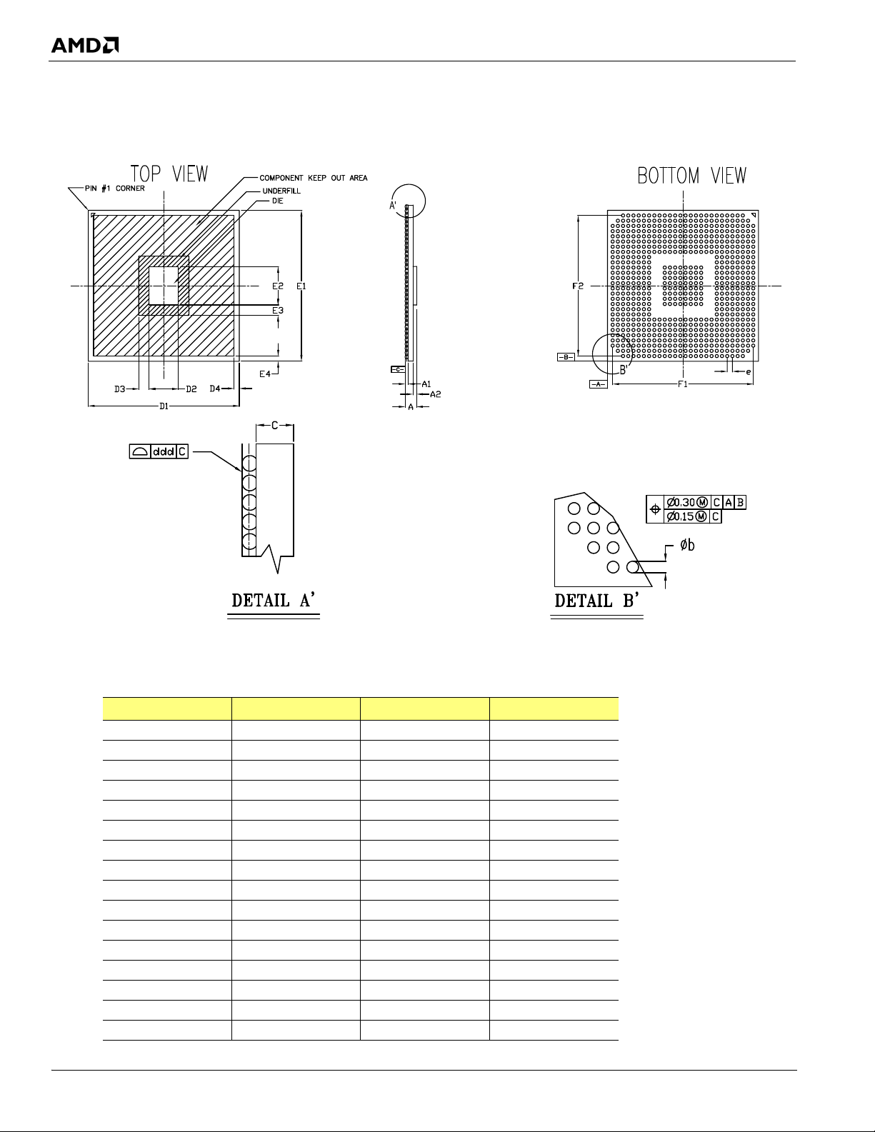
5.3 Package Information
MOD-00094-03
Figure 5-2 and Table 5-6 describe the physical dimensions of the SR5650 package. Figure 5-3 shows the detailed
ball arrangement for the SR5650.
Package Information
Figure 5-2 SR5650 692-Pin FCBGA Package Outline
Table 5-6 SR5650 692-Pin FCBGA Package Physical Dimensions
Ref. Min. (mm) Typical (mm) Max. (mm)
c 0.56 0.66 0.76
A 1.87 2.02 2.17
A1 0.40 0.50 0.60
A2 0.81 0.86 0.91
b 0.50 0.60 0.70
D1 28.80 29.00 29.20
D2 - 5.62 -
D3 2.00 - -
D4 1.00 - -
E1 28.80 29.00 29.20
E2 - 7.39 -
E3 2.00 - -
E4 1.00 - -
F1 - 27.00 -
F2 - 27.00 -
e - 1.00 -
47062 SR5650 Databook 2.10 © 2011 Advanced Micro Devices, Inc.
5-4 Proprietary
Page 47
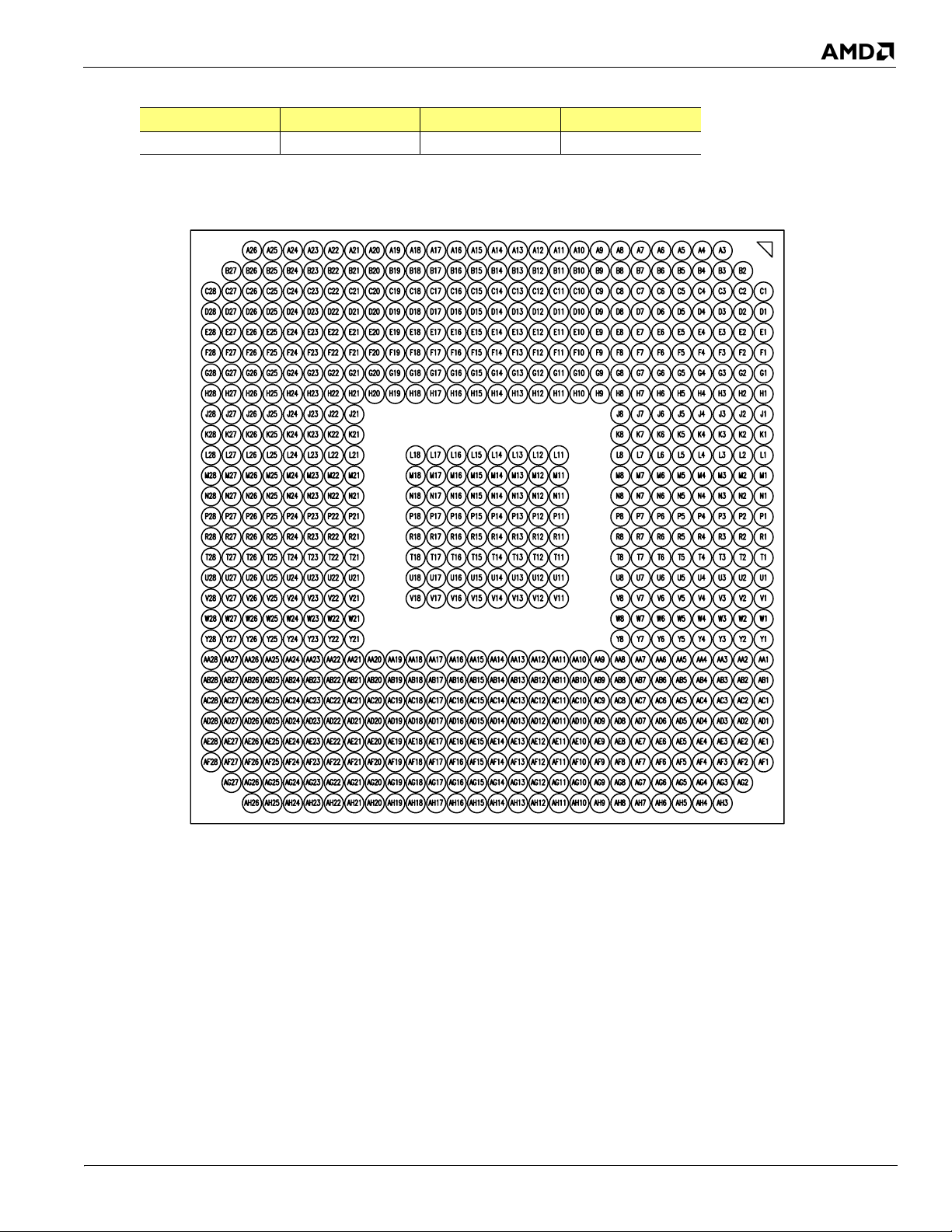
Package Information
Table 5-6 SR5650 692-Pin FCBGA Package Physical Dimensions
Ref. Min. (mm) Typical (mm) Max. (mm)
ddd - - 0.20
Note: Maximum height of SMT components is 0.650 mm.
Figure 5-3 SR5650 Ball Arrangement (Bottom View)
5.3.1 Pressure Specification
To avoid damages to the ASIC (die or solder ball joint cracks) caused by improper mechanical assembly of the cooling
device, follow the recommendations below:
• It is recommended that the maximum load that is evenly applied across the contact area between the thermal
management device and the die does not exceed 6 lbf. Note that a total load of 4-6 lbf is adequate to secure the
thermal management device and achieve the lowest thermal contact resistance with a temperature drop across
the thermal interface material of no more than 3°C. Also, the surface flatness of the metal spreader should be
0.001 inch/1 inch.
• Pre-test the assembly fixture with a strain gauge to make sure that the flexing of the final assembled board and
the pressure applying around the ASIC package will not exceed 600 micron strain under any circumstances.
© 2011 Advanced Micro Devices, Inc. 47062 SR5650 Databook 2.10
Proprietary 5-5
Page 48

• Ensure that any distortion (bow or twist) of the board after SMT and cooling device assembly is within industry
guidelines (IPC/EIA J-STD-001). For measurement method, refer to the industry approved technique described
in the manual IPC-TM-650, section 2.4.22.
5.3.2 Board Solder Reflow Process Recommendations
5.3.2.1 Stencil Opening Size for Solderball Pads on PCB
Warpage of the PCB and the package may cause solderjoint quality issues at the surface mount. Therefore, it is
recommended that the stencil opening sizes be adjusted to compensate for the warpage. The recommendation is for the
stencil aperture of the solderballs to be kept at the same size as the pads.
5.3.2.2 Reflow Profile
A reference reflow profile is given below. Please note the following when using RoHS/lead-free solder (SAC105/305/405
Tin-Silver-Cu):
• The final reflow temperature profile will depend on the type of solder paste and chemistry of flux used in the SMT
process. Modifications to the reference reflow profile may be required in order to accommodate the requirements of
the other components in the application.
• An oven with 10 heating zones or above is recommended.
• To ensure that the reflow profile meets the target specification on both sides of the board, a different profile and oven
recipe for the first and second reflow may be required.
• Mechanical stiffening can be used to minimize board warpage during reflow.
• It is suggested to decrease temperature cooling rate to minimize board warpage.
• This reflow profile applies only to RoHS/lead-free (high temperature) soldering process and it should not be used for
Eutectic solder packages. Damage may result if this condition is violated.
• Maximum 3 reflows are allowed on the same part.
Package Information
Table 5-7 Recommended Board Solder Reflow Profile - RoHS/Lead-Free Solder
Profiling Stage Temperature Process Range
Overall Preheat Room temp to 220C 2 mins to 4 mins
Soaking Time 130C to 170C Typical 60 – 80 seconds
Liquidus 220C Typical 60 – 80 seconds
Ramp Rate Ramp up and Cooling <2C / second
Peak Max. 245C 235C +/-5C
Temperature at peak
within 5C
240C to 245C 10 – 30 seconds
47062 SR5650 Databook 2.10 © 2011 Advanced Micro Devices, Inc.
5-6 Proprietary
Page 49

Package Information
Soldering Zone
45 - 90 sec. Max.
60 - 80 sec. typical
Peak Temp. (235oC+/-5% typ., 245 oC max
.)
60 – 80 sec. typical
<2.0oC / Sec.
<2.0
2 min to 4 min Max.
Solder/Part Surface Temp. ( oC )
Pre-heating Zone
Soaking Zone
130
C
170
C
60 – 120 sec. max
250
200
150
100
50
220 deg.C
o
o
o
.C / Sec.
Figure 5-4 RoHS/Lead-Free Solder (SAC305/405 Tin-Silver-Copper) Reflow Profile
Heating Time
© 2011 Advanced Micro Devices, Inc. 47062 SR5650 Databook 2.10
Proprietary 5-7
Page 50

This page is left blank intentionally.
Package Information
47062 SR5650 Databook 2.10 © 2011 Advanced Micro Devices, Inc.
5-8 Proprietary
Page 51
Power Management and ACPI
6.1 ACPI Power Management Implementation
This chapter describes the support for ACPI power management provided by the SR5650. The SR5650 system controller
supports ACPI Revision 2.0. The hardware, system BIOS, and drivers of the SR5650 have the logic required for meeting
the power management specifications of PC2001, OnNow, and the Windows Logo Program and Device Requirements
version 2.1. Table 6-1, “ACPI States Supported by the SR5650,” describes the ACPI states supported by the SR5650
system controller.
Table 6-1 ACPI States Supported by the SR5650
ACPI State Description
Processor States:
S0/C0: Working State Working State. The processor is executing instructions.
S0/C1: Halt
S0/C2: Stop Grant
Caches Snoopable
S0/C3: Stop Grant
Caches Snoopable
System States:
S1: Standby
Powered On Suspend
S3: Standby
Suspend to RAM
S4: Hibernate
Suspend to Disk
S5: Soft Off System is off. OS re-boots when the system transitions to the working state.
G3: Mechanical Off
CPU Halt state. No instructions are executed. This state has the lowest latency on resume and contributes
minimum power savings.
Stop Grant or Cache Snoopable CPU state. This state offers more power savings but has a higher latency
on resume than the C1 state.
Processor is put into the Stop Grant state. Caches are still snoopable. The HyperTransport™ link may be
disconnected and put into a low power state. System memory may be put into self-refresh.
System is in Standby mode. This state has low wakeup latency on resume. OEM support of this state is
optional.
System is off but context is saved to RAM. System memory is put into self-refresh.
System is off but context is saved to disk. When the system transitions to the working state, the OS is
resumed without a system re-boot.
Occurs when system power (AC or battery) is not present or is unable to keep the system in one of the
other states.
Chapter 6
© 2011 Advanced Micro Devices, Inc. 47062 SR5650 Databook 2.10
Proprietary 6-1
Page 52

This page intentionally left blank.
ACPI Power Management Implementation
47062 SR5650 Databook 2.10 © 2011 Advanced Micro Devices, Inc.
6-2 Proprietary
Page 53

7.1 Test Capability Features
The SR5650 system controller has integrated test modes and capabilities. These test features cover both the ASIC and
board level testing. The ASIC tests provide a very high fault coverage and low DPM (Defect Per Million) ratio of the part.
The board level tests modes can be used for motherboard manufacturing and debug purposes. The following are the test
modes of the SR5650 system controller:
• Full scan implementation on the digital core logic that provides about 97% fault coverage through ATPG
(Automatic Test Pattern Generation Vectors).
• Dedicated test logic for the on-chip custom memory macros to provide complete coverage on these modules.
• Improved access to the analog modules and PLLs in the SR5650 system controller in order to allow full
evaluation and characterization of these modules.
• A JTAG test mode (which is not entirely compliant to the IEEE 1149.1 standard) in order to allow board level
testing of neighboring devices.
• An XOR TREE test mode on all the digital I/O’s to allow for proper soldering verification at the board level.
• A VOH/VOL test mode on all digital I/O’s to allow for proper verification of output high and output low
voltages at the board level.
Chapter 7
Testability
These test modes can be accessed through the settings on the instruction register of the JTAG circuitry.
7.2 Test Interface
Table 7-1 Pins on the Test Interface
Pin Name Ball number Type Description
TESTMODE A19 I TEST_EN: Test Enable (IEEE 1149.1 test port reset)
PCIE_RESET_GPIO3 D19 I TMS: Test Mode Select (IEEE 1149.1 test mode select)
I2C_DATA C20 I TDI: Test Mode Data In (IEEE 1149.1 data in)
I2C_CLK B20 I TCLK: Test Mode Clock (IEEE 1149.1 clock)
PWM_GPIO6
PWM_GPIO4 A15 I TEST_ODD: Control ODD output in VOH/VOL test
PWM_GPIO3 F16 I TEST_EVEN: Control EVEN output in VOH/VOL test
POWERGOOD A17 I I/O Reset
B16 O TDO: Test Mode Data Out (IEEE 1149.1 data out)
7.3 XOR Tree
7.3.1 Brief Description of an XOR Tree
A sample of a generic XOR tree is shown in the figure below.
© 2011 Advanced Micro Devices, Inc. 47062 SR5650 Databook 2.10
Proprietary 7-1
Page 54

XOR Tree
XOR Start Signal
G
F
E
D
C
B
A
Figure 7-1 XOR Tree
Pin A is assigned to the output direction, and pins B through F are assigned to the input direction. It can be seen that after
all pins B to F are assigned to logic 0 or 1, a logic change in any one of these pins will toggle the output pin A.
The following is the truth table for the XOR tree shown in Figure 7-1 The XOR start signal is assumed to be logic 1.
Table 7-2 Example of an XOR Tree
Test Vector
number
10000001
21000000
31100001
41110000
51111001
61111100
71111111
Input Pin G Input Pin F Input Pin E Input Pin D Input Pin C Input Pin B Output Pin A
7.3.2 Description of the XOR Tree for the SR5650
The XOR start signal is applied at the TDI Pin of the JTAG circuitry and the output of the XOR tree is obtained at the
TDO Pin. Refer to
Section 7.3.4 for the list of the signals included on the XOR tree. There is no specific order to these
signals in the tree. A toggle of any of these balls in the XOR tree will cause the output to toggle.
7.3.3 XOR Tree Activation
To activate the XOR tree and run a XOR test, perform the sequence below:
1. Supply a 10MHz clock to I2C_CLK (Test Mode Clock) and a differential clock pair to the HT_REFCLKP/N,
GPP1_REFCLKP/N and GPP3_REFCLKP/N pins.
2. Set POWERGOOD to 0.
3. Set TESTMODE to 1.
4. Set PCIE_RESET_GPIO2 to 0.
5. Wait 5 or more I2C_CLK cycles.
6. Load JTAG instruction register with the instruction 0001 1111.
7. Load JTAG instruction register with the instruction 0010 0000.
8. Load JTAG instruction register with the instruction 0000 1000.
9. Go to Run-Test_Idle state.
10. Set POWERGOOD to 1.
47062 SR5650 Databook 2.10 © 2011 Advanced Micro Devices, Inc.
7-2 Proprietary
Page 55

XOR Tree
7.3.4 XOR Tree for the SR5650
The XOR start signal is applied at the TDI Pin of the JTAG circuitry and the output of the XOR tree is obtained at the
TDO Pin. Refer to
There is no specific order to these signals in the tree. A toggle of any of these balls in the XOR tree will cause the output
to toggle. When the XOR tree is activated, any pin on the XOR tree must be either pulled down or pulled up to the I/O
voltage of the pin. Only pins that are not on the XOR tree can be left floating.
When differential signal pairs are listed as single entries on the XOR tree, opposite input values should be applied to the
two signals in each pair (e.g., for entry no. 1 on the tree, when “1” is applied to HT_RXCAD0P, “0” should be applied to
HT_RXCAD0N).
Table 7-3 SR5650 XOR Tree
No. Pin Name Ball Ref.
1 HT_RXCAD0P/N AD28/AD27
2 HT_RXCAD1P/N AC27/AC26
3 HT_RXCAD2P/N AB28/AB27
4 HT_RXCAD3P/N AA27/AA26
5 HT_RXCAD4P/N W27/W26
6 HT_RXCAD5P/N V28/V27
7 HT_RXCAD6P/N U27/U26
8 HT_RXCAD7P/N T28/T27
9 HT_RXCTL0P/N R27/R26
10 HT_RXCAD8P/N AD25/AD24
11 HT_RXCAD9P/N AC24/AC23
12 HT_RXCAD10P/N AB25/AB24
13 HT_RXCAD11P/N AA24/AA23
14 HT_RXCAD12P/N W24/W23
15 HT_RXCAD13P/N V25/V24
16 HT_RXCAD14P/N U24/U23
17 HT_RXCAD15P/N T25/T24
18 HT_RXCTL1P/N R24/R23
19 GPP1_RX0P/N E11/F11
20 GPP1_RX1P/N D10/E10
21 GPP1_RX2P/N E9/F9
22 GPP1_RX3P/N D8/E8
23 GPP1_RX4P/N E7/F7
24 GPP1_RX5P/N D6/E6
25 GPP1_RX6P/N B5/C5
26 GPP1_RX7P/N D2/D1
27 GPP1_RX8P/N F5/F4
28 GPP1_RX9P/N G6/G5
Table 7-3 for the list of the signals included on the XOR tree.
No. Pin Name Ball Ref.
29 GPP1_RX10P/N H5/H4
30 GPP1_RX11P/N J6/J5
31 GPP1_RX12P/N K5/K4
32 GPP1_RX13P/N L6/L5
33 GPP1_RX14P/N M5/M4
34 GPP1_RX15P/N N6/N5
35 NC/NC P5/P4
36 NC/NC R6/R5
37 NC/NC T5/T4
38 NC/NC U6/U5
39 NC/NC V5/V4
40 NC/NC W6/W5
41 NC/NC Y5/Y4
42 NC/NC AA6/AA5
43 NC/NC AB5/AB4
44 NC/NC AD2/AD1
45 NC/NC AF2/AF1
46 NC/NC AF5/AG5
47 NC/NC AD6/AE6
48 NC/NC AC7/AD7
49 NC/NC AD8/AE8
50 NC/NC AC9/AD9
51 GPP3_RX0P/N AH20/AG20
52 GPP3_RX1P/N AD19/AC19
53 GPP3_RX2P/N AE18/AD18
54 GPP3_RX3P/N AD17/AC17
55 GPP3_RX4P/N AE16/AD16
56 GPP3_RX5P/N AD15/AC15
© 2011 Advanced Micro Devices, Inc. 47062 SR5650 Databook 2.10
Proprietary 7-3
Page 56

No. Pin Name Ball Ref.
57 SB_RX0P/N AG26/AH26
58 SB_RX1P/N AF25/AG25
59 SB_RX2P/N AD22/AE22
60 SB_RX3P/N AC21/AD21
61 NC/NC AE14/AD14
62 NC/NC AD13/AC13
63 NC/NC AE12/AD12
64 NC/NC AD11/AC11
65 PWM_GPIO1 E16
66 PWM_GPIO2 B15
67 PWM_GPIO3 F16
68 PWM_GPIO4 A15
69 PWM_GPIO5 C16
70 PCIE_RESET_GPIO1 B19
VOH/VOL Test
71 PCIE_RESET_GPIO4 E19
72 PCIE_RESET_GPIO5 E17
73 DFT_GPIO0 B26
74 DFT_GPIO1 A25
75 DFT_GPIO2 B24
76 DFT_GPIO3 B25
77 DFT_GPIO4 B23
78 DFT_GPIO5 A23
79 DBG_GPIO0 C22
80 DBG_GPIO1 B22
81 DBG_GPIO2 B21
82 DBG_GPIO3 A21
83 ALLOW_LDTSTOP D21
84 LDTSTOP# E15
7.4 VOH/VOL Test
7.4.1 Brief Description of a VOH/VOL Tree
The VOH/VOL logic provides signal output on I/O’s when test patterns are applied to the TEST_ODD and TEST_EVEN
pins. A sample of a generic VOH/VOL tree is shown in the figure below.
47062 SR5650 Databook 2.10 © 2011 Advanced Micro Devices, Inc.
7-4 Proprietary
Page 57
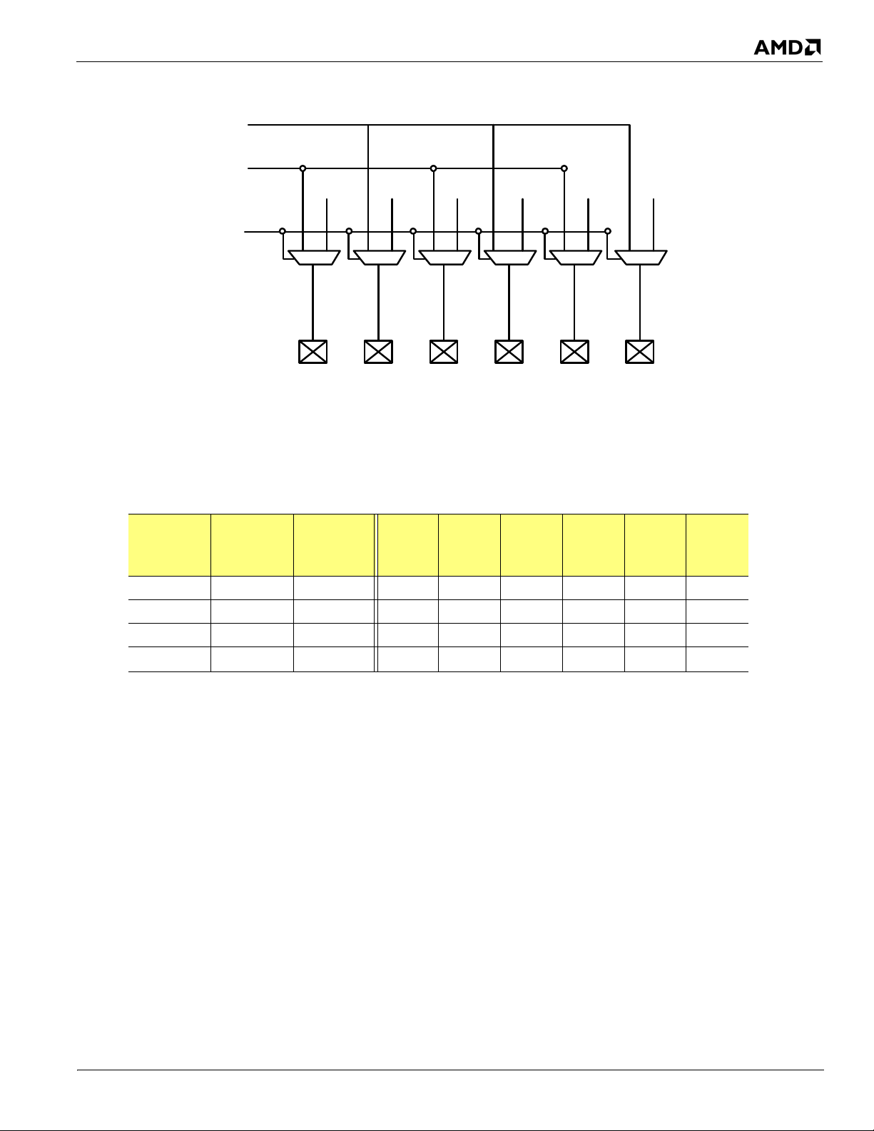
VOH/VOL Test
1
6
5
4
3
2
VOH/VOL
mode
TEST_ODD
TEST_EVEN
The following is the truth table for the above VOH/VOL tree.
Figure 7-2 Sample of a Generic VOH/VOL Tree
7.4.2 VOH/VOL Tree Activation
Table 7-4 Truth Table for the VOH/VOL Tree Outputs
Test Vector
Number
1 0 0 000000
2 0 1 010101
3 1 0 101010
4 1 1 111111
Refer to
To activate the VOH/VOL tree and run a VOH/VOL test, perform the sequence below:
1. Supply a 10MHz clock to I2C_CLK (Test Mode Clock) and a differential clock pair to the HT_REFCLKP/N,
GPP1_REFCLKP/N and GPP3_REFCLKP/N pins.
2. Set POWERGOOD to 0.
3. Set TESTMODE to 1.
4. Set PCIE_RESET_GPIO2 to 0.
5. Wait 5 or more I2C_CLK cycles.
6. Load JTAG instruction register with the instruction 0001 1111.
TEST_ODD
Input
TEST_EVEN
Input
Output
Pin 1
Output
Pin 2
Output
Pin 3
Table 7-5 below for the list of pins that are on the VOH/VOL tree.
Output
Pin 4
Output
Pin 5
Output
Pin 6
© 2011 Advanced Micro Devices, Inc. 47062 SR5650 Databook 2.10
Proprietary 7-5
7. Load JTAG instruction register with the instruction 0010 0000.
8. Load JTAG instruction register with the instruction 0101 1101.
9. Go to Run-Test_Idle state.
10. Set POWERGOOD to 1.
Page 58
7.4.3 VOH/VOL pin list
Table 7-5 below shows the SR5650 VOH/VOL Tree. There is no specific order of connection. Under the Control column,
an “Odd” or “Even” indicates that the logical output of the pin is same as the input to the “TEST_ODD” or the
“TEST_EVEN” pin respectively.
When a differential signal pair appear in the table as a single entry, the output of the positive (“P”) pin is indicated in the
Control column (see last paragraph for explanations) and the output of the negative pin (“N”) will be of the opposite
value. E.g., for entry no. 1 on the tree, when TEST_EVEN is 1, HT_TXCAD0P will give a value of 1 and HT_TXCAD0N
will give a value of 0.
Table 7-5 SR5650 VOH/VOL Tree
No. Pin Name Ball Ref. Control
1 HT_TXCAD0P/N E26/E27 Even
2 HT_TXCAD1P/N F27/F28 Odd
3 HT_TXCAD2P/N G26/G27 Even
4 HT_TXCAD3P/N H27/H28 Odd
5 HT_TXCAD4P/N K27/K28 Even
6 HT_TXCAD5P/N L26/L27 Odd
7 HT_TXCAD6P/N M27/M28 Even
8 HT_TXCAD7P/N N26/N27 Odd
9 HT_TXCTL0P/N P27/P28 Even
10 HT_TXCAD8P/N E23/E24 Odd
11 HT_TXCAD9P/N F24/F25 Even
12 HT_TXCAD10P/N G23/G24 Odd
13 HT_TXCAD11P/N H24/H25 Even
14 HT_TXCAD12P/N K24/K25 Odd
15 HT_TXCAD13P/N L23/L24 Even
16 HT_TXCAD14P/N M24/M25 Odd
17 HT_TXCAD15P/N N23/N24 Even
18 HT_TXCTL1P/N P24/P25 Odd
19 GPP1_TX0P/N B11/C11 Even
20 GPP1_TX1P/N A10/B10 Odd
21 GPP1_TX2P/N B9/C9 Even
22 GPP1_TX3P/N A8/B8 Odd
23 GPP1_TX4P/N B7/C7 Even
24 GPP1_TX5P/N A6/B6 Odd
25 GPP1_TX6P/N A4/B4 Even
26 GPP1_TX7P/N E3/E2 Odd
27 GPP1_TX8P/N F2/F1 Even
28 GPP1_TX9P/N G3/G2 Odd
29 GPP1_TX10P/N H2/H1 Even
VOH/VOL Test
No. Pin Name Ball Ref. Control
30 GPP1_TX11P/N J3/J2 Odd
31 GPP1_TX12P/N K2/K1 Even
32 GPP1_TX13P/N L3/L2 Odd
33 GPP1_TX14P/N M2/M1 Even
34 GPP1_TX15P/N N3/N2 Odd
35 NC/NC P2/P1 Even
36 NC/NC R3/R2 Odd
37 NC/NC T2/T1 Even
38 NC/NC U3/U2 Odd
39 NC/NC V2/V1 Even
40 NC/NC W3/W2 Odd
41 NC/NC Y2/Y1 Even
42 NC/NC AA3/AA2 Odd
43 NC/NC AB2/AB1 Even
44 NC/NC AC3/AC2 Odd
45 NC/NC AE3/AE2 Even
46 NC/NC AG4/AH4 Odd
47 NC/NC AG6/AH6 Even
48 NC/NC AF7/AG7 Odd
49 NC/NC AG8/AH8 Even
50 NC/NC AF9/AG9 Odd
51 GPP3_TX0P/N AG19/AF19 Even
52 GPP3_TX1P/N AH18/AG18 Odd
53 GPP3_TX2P/N AG17/AF17 Even
54 GPP3_TX3P/N AH16/AG16 Odd
55 GPP3_TX4P/N AG15/AF15 Even
56 GPP3_TX5P/N AH14/AG14 Odd
57 SB_TX0P/N AG24/AH24 Even
58 SB_TX1P/N AF23/AG23 Odd
47062 SR5650 Databook 2.10 © 2011 Advanced Micro Devices, Inc.
7-6 Proprietary
Page 59

VOH/VOL Test
No. Pin Name Ball Ref. Control
59 SB_TX2P/N AF21/AG21 Even
60 SB_TX3P/N AG22/AH22 Odd
61 NC/NC AG13/AF13 Even
62 NC/NC AH12/AG12 Odd
63 NC/NC AG11/AF11 Even
64 NC/NC AH10/AG10 Odd
65 PWM_GPIO1 E16 Even
66 PWM_GPIO2 B15 Odd
67 PWM_GPIO5 C16 Even
68 PCIE_RESET_GPIO1 B19 Odd
69 PCIE_RESET_GPIO4 E19 Even
70 PCIE_RESET_GPIO5 E17 Odd
71 DFT_GPIO0 B26 Even
72 DFT_GPIO1 A25 Odd
73 DFT_GPIO2 B24 Even
74 DFT_GPIO3 B25 Odd
75 DFT_GPIO4 B23 Even
76 DFT_GPIO5 A23 Odd
77 DBG_GPIO0 C22 Even
78 DBG_GPIO1 B22 Odd
79 DBG_GPIO2 B21 Even
80 DBG_GPIO3 A21 Odd
81 ALLOW_LDTSTOP D21 Even
82 LDTSTOP# E15 Odd
© 2011 Advanced Micro Devices, Inc. 47062 SR5650 Databook 2.10
Proprietary 7-7
Page 60

This page intentionally left blank.
VOH/VOL Test
47062 SR5650 Databook 2.10 © 2011 Advanced Micro Devices, Inc.
7-8 Proprietary
Page 61

Appendix A
Pin Listings
This appendix contains pin listings for the SR5650 sorted in different ways. To go to the listing of interest, use the linked
cross-references below:
“SR5650 Pin Listing Sorted by Ball Reference” on page A-2
“SR5650 Pin Listing Sorted by Pin Name” on page A-9
© 2011 Advanced Micro Devices, Inc. 47062 SR5650 Databook 2.10
Proprietary Appendix A-1
Page 62
A.1 SR5650 Pin Listing Sorted by Ball Reference
Table A-1 SR5650 Pin Listing Sorted by Ball Reference
Ball # Ball Name
A10 GPP1_TX1P
A11 VSS
A12 VDDA18PCIE
A13 VDDA18PCIE
A14 VSS
A15 PWM_GPIO4
A16 VSS
A17 POWERGOOD
A18 VDD18
A19 TESTMODE
A20 VSS
A21
A22 VSS
A23
A24 VSS
A25 DFT_GPIO1
A26 VSS
A3 VDDPCIE
A4 GPP1_TX6P
A5 VSS
A6 GPP1_TX5P
A7 VSS
A8 GPP1_TX3P
A9 VSS
AA1 VSS
AA10 VDDPCIE
AA11 VSS
AA12 VDDPCIE
AA13 VSS
AA14 GPP3_REFCLKN
AA15 GPP3_REFCLKP
AA16 VDDPCIE
AA17 VSS
DBG_GPIO3/
NON_FATAL_CORR#
DFT_GPIO5/
SYNCFLOODIN#
Ball # Ball Name
AA18 VDDPCIE
AA19 VSS
AA2 NC
AA20 VSS
AA21 THERMALDIODE_N
AA22 VDDHT
AA23 HT_RXCAD11N
AA24 HT_RXCAD11P
AA25 VSS
AA26 HT_RXCAD3N
AA27 HT_RXCAD3P
AA28 VSS
AA3 NC
AA4 VSS
AA5 NC
AA6 NC
AA7 VSS
AA8 VDDPCIE
AA9 VSS
AB1 NC
AB10 VSS
AB11 VDDPCIE
AB12 VSS
AB13 VDDPCIE
AB14 VSS
AB15 VDDPCIE
AB16 VSS
AB17 VDDPCIE
AB18 VSS
AB19 VDDPCIE
AB2 NC
AB20 VSS
AB21 VSS
AB22 VDDHT
SR5650 Pin Listing Sorted by Ball Reference
Ball # Ball Name
AB23 VSS
AB24 HT_RXCAD10N
AB25 HT_RXCAD10P
AB26 VSS
AB27 HT_RXCAD2N
AB28 HT_RXCAD2P
AB3 VSS
AB4 NC
AB5 NC
AB6 VSS
AB7 VDDPCIE
AB8 VSS
AB9 VDDPCIE
AC1 VSS
AC10 VSS
AC11 NC
AC12 VSS
AC13 NC
AC14 VSS
AC15 GPP3_RX5N
AC16 VSS
AC17 GPP3_RX3N
AC18 VSS
AC19 GPP3_RX1N
AC2 NC
AC20 VSS
AC21 SB_RX3P
AC22 VDDHT
AC23 HT_RXCAD9N
AC24 HT_RXCAD9P
AC25 VSS
AC26 HT_RXCAD1N
AC27 HT_RXCAD1P
AC28 VSS
47062 SR5650 Databook 2.10 © 2011 Advanced Micro Devices, Inc.
Appendix A-2 Proprietary
Page 63
SR5650 Pin Listing Sorted by Ball Reference
Ball # Ball Name
AC3 NC
AC4 VSS
AC5 VSS
AC6 VDDPCIE
AC7 NC
AC8 VSS
AC9 NC
AD1 NC
AD10 PCE_RCALRN
AD11 NC
AD12 NC
AD13 NC
AD14 NC
AD15 GPP3_RX5P
AD16 GPP3_RX4N
AD17 GPP3_RX3P
Ball # Ball Name
AE11 VSS
AE12 NC
AE13 VSS
AE14 NC
AE15 VSS
AE16 GPP3_RX4P
AE17 VSS
AE18 GPP3_RX2P
AE19 VSS
AE2 NC
AE20 PCE_BCALRP
AE21 VSS
AE22 SB_RX2N
AE23 VSS
AE24 VDDHT
AE25 VDDHT
Ball # Ball Name
AF2 NC
AF20 VSS
AF21 SB_TX2P
AF22 VSS
AF23 SB_TX1P
AF24 VSS
AF25 SB_RX1P
AF26 VSS
AF27 VDDHT
AF28 VSS
AF3 VDDPCIE
AF4 VSS
AF5 NC
AF6 VSS
AF7 NC
AF8 VSS
AD18 GPP3_RX2N
AD19 GPP3_RX1P
AD2 NC
AD20 PCE_BCALRN
AD21 SB_RX3N
AD22 SB_RX2P
AD23 VDDHT
AD24 HT_RXCAD8N
AD25 HT_RXCAD8P
AD26 VSS
AD27 HT_RXCAD0N
AD28 HT_RXCAD0P
AD3 VSS
AD4 VSS
AD5 VDDPCIE
AD6 NC
AD7 NC
AE26 VDDHT
AE27 VDDHT
AE28 VDDHT
AE3 NC
AE4 VDDPCIE
AE5 VSS
AE6 NC
AE7 VSS
AE8 NC
AE9 VSS
AF1 NC
AF10 VSS
AF11 NC
AF12 VSS
AF13 NC
AF14 VSS
AF15 GPP3_TX4N
AF9 NC
AG10 NC
AG11 NC
AG12 NC
AG13 NC
AG14 GPP3_TX5N
AG15 GPP3_TX4P
AG16 GPP3_TX3N
AG17 GPP3_TX2P
AG18 GPP3_TX1N
AG19 GPP3_TX0P
AG2 VDDPCIE
AG20 GPP3_RX0N
AG21 SB_TX2N
AG22 SB_TX3P
AG23 SB_TX1N
AG24 SB_TX0P
AD8 NC
AD9 NC
AE1 VSS
AE10 PCE_RCALRP
AF16 VSS
AF17 GPP3_TX2N
AF18 VSS
AF19 GPP3_TX0N
AG25 SB_RX1N
AG26 SB_RX0P
AG27 VSS
AG3 VSS
© 2011 Advanced Micro Devices, Inc. 47062 SR5650 Databook 2.10
Proprietary Appendix A-3
Page 64

SR5650 Pin Listing Sorted by Ball Reference
Ball # Ball Name
AG4 NC
AG5 NC
AG6 NC
AG7 NC
AG8 NC
AG9 NC
AH10 NC
AH11 VSS
AH12 NC
AH13 VSS
AH14 GPP3_TX5P
AH15 VSS
AH16 GPP3_TX3P
AH17 VSS
AH18 GPP3_TX1P
AH19 VSS
Ball # Ball Name
B16 PWM_GPIO6
B17 OSCIN
B18 VDD18
B19 PCIE_RESET_GPIO1
B2 VDDPCIE
B20 I2C_CLK
B21 DBG_GPIO2
B22 DBG_GPIO1
B23 DFT_GPIO4
B24 DFT_GPIO2
B25 DFT_GPIO3
B26 DFT_GPIO0/NMI#
B27 VSS
B3 VSS
B4 GPP1_TX6N
B5 GPP1_RX6P
Ball # Ball Name
C23 VSS
C24 VDDHTTX
C25 VDDHTTX
C26 VDDHTTX
C27 VDDHTTX
C28 VDDHTTX
C3 VDDPCIE
C4 VSS
C5 GPP1_RX6N
C6 VSS
C7 GPP1_TX4N
C8 VSS
C9 GPP1_TX2N
D1 GPP1_RX7N
D10 GPP1_RX1P
D11 VSS
AH20 GPP3_RX0P
AH21 VSS
AH22 SB_TX3N
AH23 VSS
AH24 SB_TX0N
AH25 VSS
AH26 SB_RX0N
AH3 VSS
AH4 NC
AH5 VSS
AH6 NC
AH7 VSS
AH8 NC
AH9 VSS
B10 GPP1_TX1N
B11 GPP1_TX0P
B12 VDDA18PCIE
B6 GPP1_TX5N
B7 GPP1_TX4P
B8 GPP1_TX3N
B9 GPP1_TX2P
C1 VDDPCIE
C10 VSS
C11 GPP1_TX0N
C12 VDDA18PCIE
C13 VDDA18PCIE
C14 VSS
C15 VSS
C16 PWM_GPIO5
C17 VSS
C18 VDD18
C19 VSS
C2 VSS
C20 I2C_DATA
D12 VDDA18PCIE
D13 VDDA18PCIE
D14 VSS
D15 SYSRESET#
D16 VSS
D17 PCIE_RESET_GPIO2
D18 VDD18
D19 PCIE_RESET_GPIO3
D2 GPP1_RX7P
D20 VSS
D21 ALLOW_LDTSTOP
D22 VDDHTTX
D23 VDDHTTX
D24 HT_RXCALN
D25 HT_RXCALP
D26 VSS
D27 HT_TXCALN
B13 VDDA18PCIE
B14 VSS
B15 PWM_GPIO2
C21 VSS
C22
DBG_GPIO0/SERR_F
ATAL #
D28 HT_TXCALP
D3 VSS
D4 VDDPCIE
47062 SR5650 Databook 2.10 © 2011 Advanced Micro Devices, Inc.
Appendix A-4 Proprietary
Page 65

SR5650 Pin Listing Sorted by Ball Reference
Ball # Ball Name
D5 VSS
D6 GPP1_RX5P
D7 VSS
D8 GPP1_RX3P
D9 VSS
E1 VSS
E10 GPP1_RX1N
E11 GPP1_RX0P
E12 VDDA18PCIE
E13 VDDA18PCIE
E14 PCE_TCALRN
E15 LDTSTOP#
E16 PWM_GPIO1
E17 PCIE_RESET_GPIO5
E18 VDD18
E19 PCIE_RESET_GPIO4
Ball # Ball Name
F12 VDDA18PCIE
F13 VDDA18PCIE
F14 PCE_TCALRP
F15 VSS
F16 PWM_GPIO3
F17 VSS
F18 VSS
F19 VSS
F2 GPP1_TX8P
F20 VSS
F21 VSS
F22 VDDHTTX
F23 VSS
F24 HT_TXCAD9P
F25 HT_TXCAD9N
F26 VSS
Ball # Ball Name
G2 GPP1_TX9N
G20 VSS
G21 VDDA18HTPLL
G22 VDDHTTX
G23 HT_TXCAD10P
G24 HT_TXCAD10N
G25 VSS
G26 HT_TXCAD2P
G27 HT_TXCAD2N
G28 VSS
G3 GPP1_TX9P
G4 VSS
G5 GPP1_RX9N
G6 GPP1_RX9P
G7 VDDPCIE
G8 VDDPCIE
E2 GPP1_TX7N
E20 VSS
E21 STRP_DATA
E22 VDDHTTX
E23 HT_TXCAD8P
E24 HT_TXCAD8N
E25 VSS
E26 HT_TXCAD0P
E27 HT_TXCAD0N
E28 VSS
E3 GPP1_TX7P
E4 VSS
E5 VDDPCIE
E6 GPP1_RX5N
E7 GPP1_RX4P
E8 GPP1_RX3N
E9 GPP1_RX2P
F27 HT_TXCAD1P
F28 HT_TXCAD1N
F3 VSS
F4 GPP1_RX8N
F5 GPP1_RX8P
F6 VDDPCIE
F7 GPP1_RX4N
F8 VSS
F9 GPP1_RX2N
G1 VSS
G10 VDDPCIE
G11 VSS
G12 VDDA18PCIE
G13 VDDA18PCIE
G14 VDDA18PCIE
G15 VSS
G16 VSS
G9 VSS
H1 GPP1_TX10N
H10 VSS
H11 VDDPCIE
H12 VDDA18PCIE
H13 VDDA18PCIE
H14 VDDA18PCIE
H15 VSS
H16 VSS
H17 VSS
H18 VSS
H19 VSS
H2 GPP1_TX10P
H20 VSS
H21 VSS
H22 VDDHTTX
H23 VSS
F1 GPP1_TX8N
F10 VSS
F11 GPP1_RX0N
G17 VSS
G18 VSS
G19 VSS
H24 HT_TXCAD11P
H25 HT_TXCAD11N
H26 VSS
© 2011 Advanced Micro Devices, Inc. 47062 SR5650 Databook 2.10
Proprietary Appendix A-5
Page 66

SR5650 Pin Listing Sorted by Ball Reference
Ball # Ball Name
H27 HT_TXCAD3P
H28 HT_TXCAD3N
H3 VSS
H4 GPP1_RX10N
H5 GPP1_RX10P
H6 VSS
H7 VDDPCIE
H8 GPP1_REFCLKN
H9 VDDPCIE
J1 VSS
J2 GPP1_TX11N
J21 HT_REFCLKN
J22 VSS
J23 HT_TXCLK1P
J24 HT_TXCLK1N
J25 VSS
Ball # Ball Name
K4 GPP1_RX12N
K5 GPP1_RX12P
K6 VSS
K7 VDDPCIE
K8 VSS
L1 VSS
L11 VDDA18PCIE
L12 VSS
L13 VSS
L14 VDDC
L15 VSS
L16 VDDC
L17 VSS
L18 VSS
L2 GPP1_TX13N
L21 VDDHT
Ball # Ball Name
M17 VSS
M18 VSS
M2 GPP1_TX14P
M21 VSS
M22 VDDHT
M23 VSS
M24 HT_TXCAD14P
M25 HT_TXCAD14N
M26 VSS
M27 HT_TXCAD6P
M28 HT_TXCAD6N
M3 VSS
M4 GPP1_RX14N
M5 GPP1_RX14P
M6 VSS
M7 VDDPCIE
J26 HT_TXCLK0P
J27 HT_TXCLK0N
J28 VSS
J3 GPP1_TX11P
J4 VSS
J5 GPP1_RX11N
J6 GPP1_RX11P
J7 VSS
J8 GPP1_REFCLKP
K1 GPP1_TX12N
K2 GPP1_TX12P
K21 HT_REFCLKP
K22 VDDHT
K23 VSS
K24 HT_TXCAD12P
K25 HT_TXCAD12N
K26 VSS
L22 VSS
L23 HT_TXCAD13P
L24 HT_TXCAD13N
L25 VSS
L26 HT_TXCAD5P
L27 HT_TXCAD5N
L28 VSS
L3 GPP1_TX13P
L4 VSS
L5 GPP1_RX13N
L6 GPP1_RX13P
L7 VSS
L8 VDDPCIE
M1 GPP1_TX14N
M11 VSS
M12 VSS
M13 VDDC
M8 VSS
N1 VSS
N11 VSS
N12 VDDC
N13 VSS
N14 VDDC
N15 VSS
N16 VDDC
N17 VSS
N18 VSS
N2 GPP1_TX15N
N21 VDDHT
N22 VSS
N23 HT_TXCAD15P
N24 HT_TXCAD15N
N25 VSS
N26 HT_TXCAD7P
K27 HT_TXCAD4P
K28 HT_TXCAD4N
K3 VSS
M14 VSS
M15 VDDC
M16 VSS
N27 HT_TXCAD7N
N28 VSS
N3 GPP1_TX15P
47062 SR5650 Databook 2.10 © 2011 Advanced Micro Devices, Inc.
Appendix A-6 Proprietary
Page 67

SR5650 Pin Listing Sorted by Ball Reference
Ball # Ball Name
N4 VSS
N5 GPP1_RX15N
N6 GPP1_RX15P
N7 VSS
N8 VDDPCIE
P1 NC
P11 VSS
P12 VSS
P13 VDDC
P14 VSS
P15 VDDC
P16 VSS
P17 VDDC
P18 VSS
P2 NC
P21 VSS
Ball # Ball Name
R17 VSS
R18 VSS
R2 NC
R21 VDDHT
R22 VSS
R23 HT_RXCTL1N
R24 HT_RXCTL1P
R25 VSS
R26 HT_RXCTL0N
R27 HT_RXCTL0P
R28 VSS
R3 NC
R4 VSS
R5 NC
R6 NC
R7 VSS
Ball # Ball Name
T4 NC
T5 NC
T6 VSS
T7 VDDPCIE
T8 VSS
U1 VSS
U11 VSS
U12 VSS
U13 VSS
U14 VDDC
U15 VSS
U16 VDDC
U17 VSS
U18 VSS
U2 NC
U21 VDDHT
P22 VDDHT
P23 VSS
P24 HT_TXCTL1P
P25 HT_TXCTL1N
P26 VSS
P27 HT_TXCTL0P
P28 HT_TXCTL0N
P3 VSS
P4 NC
P5 NC
P6 VSS
P7 VDDPCIE
P8 VSS
R1 VSS
R11 VSS
R12 VDDC
R13 VSS
R8 VDDPCIE
T1 NC
T11 VSS
T12 VSS
T13 VDDC
T14 VSS
T15 VDDC
T16 VSS
T17 VDDC
T18 VSS
T2 NC
T21 VSS
T22 VDDHT
T23 VSS
T24 HT_RXCAD15N
T25 HT_RXCAD15P
T26 VSS
U22 VSS
U23 HT_RXCAD14N
U24 HT_RXCAD14P
U25 VSS
U26 HT_RXCAD6N
U27 HT_RXCAD6P
U28 VSS
U3 NC
U4 VSS
U5 NC
U6 NC
U7 VSS
U8 NC
V1 NC
V11 VDDA18PCIE
V12 VSS
V13 VSS
R14 VDDC
R15 VSS
R16 VDDC
T27 HT_RXCAD7N
T28 HT_RXCAD7P
T3 VSS
V14 VSS
V15 VSS
V16 VSS
© 2011 Advanced Micro Devices, Inc. 47062 SR5650 Databook 2.10
Proprietary Appendix A-7
Page 68

SR5650 Pin Listing Sorted by Ball Reference
Ball # Ball Name
V17 VSS
V18 VDDA18PCIE
V2 NC
V21 VSS
V22 VDDHT
V23 VSS
V24 HT_RXCAD13N
V25 HT_RXCAD13P
V26 VSS
V27 HT_RXCAD5N
V28 HT_RXCAD5P
V3 VSS
V4 NC
V5 NC
V6 VSS
V7 VDDPCIE
Ball # Ball Name
Y22 VDDHT
Y23 VSS
Y24 HT_RXCLK1N
Y25 HT_RXCLK1P
Y26 VSS
Y27 HT_RXCLK0N
Y28 HT_RXCLK0P
Y3 VSS
Y4 NC
Y5 NC
Y6 VSS
Y7 VDDPCIE
Y8 VSS
V8 NC
W1 VSS
W2 NC
W21 VDDHT
W22 VSS
W23 HT_RXCAD12N
W24 HT_RXCAD12P
W25 VSS
W26 HT_RXCAD4N
W27 HT_RXCAD4P
W28 VSS
W3 NC
W4 VSS
W5 NC
W6 NC
W7 VSS
W8 VDDPCIE
Y1 NC
Y2 NC
Y21 THERMALDIODE_P
47062 SR5650 Databook 2.10 © 2011 Advanced Micro Devices, Inc.
Appendix A-8 Proprietary
Page 69

SR5650 Pin Listing Sorted by Ball Reference
A.2 SR5650 Pin Listing Sorted by Pin Name
Ball Name Ball #
ALLOW_LDTSTOP D21
DBG_GPIO0/SERR_F
ATAL #
DBG_GPIO1 B22
DBG_GPIO2 B21
DBG_GPIO3/
NON_FATAL_CORR#
DFT_GPIO0/NMI# B26
DFT_GPIO1 A25
DFT_GPIO2 B24
DFT_GPIO3 B25
DFT_GPIO4 B23
DFT_GPIO5/
SYNCFLOODIN#
GPP1_REFCLKN H8
GPP1_REFCLKP J8
GPP1_RX0N F11
GPP1_RX0P E11
GPP1_RX10N H4
GPP1_RX10P H5
GPP1_RX11N J5
GPP1_RX11P J6
GPP1_RX12N K4
GPP1_RX12P K5
GPP1_RX13N L5
GPP1_RX13P L6
GPP1_RX14N M4
GPP1_RX14P M5
GPP1_RX15N N5
GPP1_RX15P N6
GPP1_RX1N E10
GPP1_RX1P D10
GPP1_RX2N F9
GPP1_RX2P E9
GPP1_RX3N E8
GPP1_RX3P D8
C22
A21
A23
Ball Name Ball #
GPP1_RX4N F7
GPP1_RX4P E7
GPP1_RX5N E6
GPP1_RX5P D6
GPP1_RX6N C5
GPP1_RX6P B5
GPP1_RX7N D1
GPP1_RX7P D2
GPP1_RX8N F4
GPP1_RX8P F5
GPP1_RX9N G5
GPP1_RX9P G6
GPP1_TX0N C11
GPP1_TX0P B11
GPP1_TX10N H1
GPP1_TX10P H2
GPP1_TX11N J2
GPP1_TX11P J3
GPP1_TX12N K1
GPP1_TX12P K2
GPP1_TX13N L2
GPP1_TX13P L3
GPP1_TX14N M1
GPP1_TX14P M2
GPP1_TX15N N2
GPP1_TX15P N3
GPP1_TX1N B10
GPP1_TX1P A10
GPP1_TX2N C9
GPP1_TX2P B9
GPP1_TX3N B8
GPP1_TX3P A8
GPP1_TX4N C7
GPP1_TX4P B7
GPP1_TX5N B6
Ball Name Ball #
GPP1_TX5P A6
GPP1_TX6N B4
GPP1_TX6P A4
GPP1_TX7N E2
GPP1_TX7P E3
GPP1_TX8N F1
GPP1_TX8P F2
GPP1_TX9N G2
GPP1_TX9P G3
GPP3_REFCLKN AA14
GPP3_REFCLKP AA15
GPP3_RX0N AG20
GPP3_RX0P AH20
GPP3_RX1N AC19
GPP3_RX1P AD19
GPP3_RX2N AD18
GPP3_RX2P AE18
GPP3_RX3N AC17
GPP3_RX3P AD17
GPP3_RX4N AD16
GPP3_RX4P AE16
GPP3_RX5N AC15
GPP3_RX5P AD15
GPP3_TX0N AF19
GPP3_TX0P AG19
GPP3_TX1N AG18
GPP3_TX1P AH18
GPP3_TX2N AF17
GPP3_TX2P AG17
GPP3_TX3N AG16
GPP3_TX3P AH16
GPP3_TX4N AF15
GPP3_TX4P AG15
GPP3_TX5N AG14
GPP3_TX5P AH14
© 2011 Advanced Micro Devices, Inc. 47062 SR5650 Databook 2.10
Proprietary Appendix A-9
Page 70

SR5650 Pin Listing Sorted by Ball Reference
Ball Name Ball #
HT_REFCLKN J21
HT_REFCLKP K21
HT_RXCAD0N AD27
HT_RXCAD0P AD28
HT_RXCAD10N AB24
HT_RXCAD10P AB25
HT_RXCAD11N AA23
HT_RXCAD11P AA24
HT_RXCAD12N W23
HT_RXCAD12P W24
HT_RXCAD13N V24
HT_RXCAD13P V25
HT_RXCAD14N U23
HT_RXCAD14P U24
HT_RXCAD15N T24
HT_RXCAD15P T25
Ball Name Ball #
HT_RXCLK0N Y27
HT_RXCLK0P Y28
HT_RXCLK1N Y24
HT_RXCLK1P Y25
HT_RXCTL0N R26
HT_RXCTL0P R27
HT_RXCTL1N R23
HT_RXCTL1P R24
HT_TXCAD0N E27
HT_TXCAD0P E26
HT_TXCAD10N G24
HT_TXCAD10P G23
HT_TXCAD11N H25
HT_TXCAD11P H24
HT_TXCAD12N K25
HT_TXCAD12P K24
Ball Name Ball #
HT_TXCAD8N E24
HT_TXCAD8P E23
HT_TXCAD9N F25
HT_TXCAD9P F24
HT_TXCALN D27
HT_TXCALP D28
HT_TXCLK0N J27
HT_TXCLK0P J26
HT_TXCLK1N J24
HT_TXCLK1P J23
HT_TXCTL0N P28
HT_TXCTL0P P27
HT_TXCTL1N P25
HT_TXCTL1P P24
I2C_CLK B20
I2C_DATA C20
HT_RXCAD1N AC26
HT_RXCAD1P AC27
HT_RXCAD2N AB27
HT_RXCAD2P AB28
HT_RXCAD3N AA26
HT_RXCAD3P AA27
HT_RXCAD4N W26
HT_RXCAD4P W27
HT_RXCAD5N V27
HT_RXCAD5P V28
HT_RXCAD6N U26
HT_RXCAD6P U27
HT_RXCAD7N T27
HT_RXCAD7P T28
HT_RXCAD8N AD24
HT_RXCAD8P AD25
HT_RXCAD9N AC23
HT_TXCAD13N L24
HT_TXCAD13P L23
HT_TXCAD14N M25
HT_TXCAD14P M24
HT_TXCAD15N N24
HT_TXCAD15P N23
HT_TXCAD1N F28
HT_TXCAD1P F27
HT_TXCAD2N G27
HT_TXCAD2P G26
HT_TXCAD3N H28
HT_TXCAD3P H27
HT_TXCAD4N K28
HT_TXCAD4P K27
HT_TXCAD5N L27
HT_TXCAD5P L26
HT_TXCAD6N M28
LDTSTOP# E15
NC AA2
NC AA3
NC AA5
NC AA6
NC AB1
NC AB2
NC AB4
NC AB5
NC AC11
NC AC13
NC AC2
NC AC3
NC AC7
NC AC9
NC AD1
NC AD11
HT_RXCAD9P AC24
HT_RXCALN D24
HT_RXCALP D25
HT_TXCAD6P M27
HT_TXCAD7N N27
HT_TXCAD7P N26
NC AD12
NC AD13
NC AD14
47062 SR5650 Databook 2.10 © 2011 Advanced Micro Devices, Inc.
Appendix A-10 Proprietary
Page 71

SR5650 Pin Listing Sorted by Ball Reference
Ball Name Ball #
NC AD2
NC AD6
NC AD7
NC AD8
NC AD9
NC AE12
NC AE14
NC AE2
NC AE3
NC AE6
NC AE8
NC AF1
NC AF11
NC AF13
NC AF2
NC AF5
Ball Name Ball #
NC P5
NC R2
NC R3
NC R5
NC R6
NC T1
NC T2
NC T4
NC T5
NC U2
NC U3
NC U5
NC U6
NC U8
NC V1
NC V2
Ball Name Ball #
PCIE_RESET_GPIO3 D19
PCIE_RESET_GPIO4 E19
PCIE_RESET_GPIO5 E17
POWERGOOD A17
PWM_GPIO1 E16
PWM_GPIO2 B15
PWM_GPIO3 F16
PWM_GPIO4 A15
PWM_GPIO5 C16
PWM_GPIO6 B16
SB_RX0N AH26
SB_RX0P AG26
SB_RX1N AG25
SB_RX1P AF25
SB_RX2N AE22
SB_RX2P AD22
NC AF7
NC AF9
NC AG10
NC AG11
NC AG12
NC AG13
NC AG4
NC AG5
NC AG6
NC AG7
NC AG8
NC AG9
NC AH10
NC AH12
NC AH4
NC AH6
NC AH8
NC V4
NC V5
NC V8
NC W2
NC W3
NC W5
NC W6
NC Y1
NC Y2
NC Y4
NC Y5
OSCIN B17
PCE_BCALRN AD20
PCE_BCALRP AE20
PCE_RCALRN AD10
PCE_RCALRP AE10
PCE_TCALRN E14
SB_RX3N AD21
SB_RX3P AC21
SB_TX0N AH24
SB_TX0P AG24
SB_TX1N AG23
SB_TX1P AF23
SB_TX2N AG21
SB_TX2P AF21
SB_TX3N AH22
SB_TX3P AG22
STRP_DATA E21
SYSRESET# D15
TESTMODE A19
THERMALDIODE_N AA21
THERMALDIODE_P Y21
VDD18 A18
VDD18 B18
NC P1
NC P2
NC P4
PCE_TCALRP F14
PCIE_RESET_GPIO1 B19
PCIE_RESET_GPIO2 D17
VDD18 C18
VDD18 D18
VDD18 E18
© 2011 Advanced Micro Devices, Inc. 47062 SR5650 Databook 2.10
Proprietary Appendix A-11
Page 72

SR5650 Pin Listing Sorted by Ball Reference
Ball Name Ball #
VDDA18HTPLL G21
VDDA18PCIE A12
VDDA18PCIE A13
VDDA18PCIE B12
VDDA18PCIE B13
VDDA18PCIE C12
VDDA18PCIE C13
VDDA18PCIE D12
VDDA18PCIE D13
VDDA18PCIE E12
VDDA18PCIE E13
VDDA18PCIE F12
VDDA18PCIE F13
VDDA18PCIE G12
VDDA18PCIE G13
VDDA18PCIE G14
Ball Name Ball #
VDDC T15
VDDC T17
VDDC U14
VDDC U16
VDDHT AA22
VDDHT AB22
VDDHT AC22
VDDHT AD23
VDDHT AE24
VDDHT AE25
VDDHT AE26
VDDHT AE27
VDDHT AE28
VDDHT AF27
VDDHT K22
VDDHT L21
Ball Name Ball #
VDDPCIE A3
VDDPCIE AA10
VDDPCIE AA12
VDDPCIE AA16
VDDPCIE AA18
VDDPCIE AA8
VDDPCIE AB11
VDDPCIE AB13
VDDPCIE AB15
VDDPCIE AB17
VDDPCIE AB19
VDDPCIE AB7
VDDPCIE AB9
VDDPCIE AC6
VDDPCIE AD5
VDDPCIE AE4
VDDA18PCIE H12
VDDA18PCIE H13
VDDA18PCIE H14
VDDA18PCIE L11
VDDA18PCIE V11
VDDA18PCIE V18
VDDC L14
VDDC L16
VDDC M13
VDDC M15
VDDC N12
VDDC N14
VDDC N16
VDDC P13
VDDC P15
VDDC P17
VDDC R12
VDDHT M22
VDDHT N21
VDDHT P22
VDDHT R21
VDDHT T22
VDDHT U21
VDDHT V22
VDDHT W21
VDDHT Y22
VDDHTTX C24
VDDHTTX C25
VDDHTTX C26
VDDHTTX C27
VDDHTTX C28
VDDHTTX D22
VDDHTTX D23
VDDHTTX E22
VDDPCIE AF3
VDDPCIE AG2
VDDPCIE B2
VDDPCIE C1
VDDPCIE C3
VDDPCIE D4
VDDPCIE E5
VDDPCIE F6
VDDPCIE G10
VDDPCIE G7
VDDPCIE G8
VDDPCIE H11
VDDPCIE H7
VDDPCIE H9
VDDPCIE K7
VDDPCIE L8
VDDPCIE M7
VDDC R14
VDDC R16
VDDC T13
VDDHTTX F22
VDDHTTX G22
VDDHTTX H22
VDDPCIE N8
VDDPCIE P7
VDDPCIE R8
47062 SR5650 Databook 2.10 © 2011 Advanced Micro Devices, Inc.
Appendix A-12 Proprietary
Page 73
SR5650 Pin Listing Sorted by Ball Reference
Ball Name Ball #
VDDPCIE T7
VDDPCIE V7
VDDPCIE W8
VDDPCIE Y7
VSS A11
VSS A14
VSS A16
VSS A20
VSS A22
VSS A24
VSS A26
VSS A5
VSS A7
VSS A9
VSS AA1
VSS AA11
Ball Name Ball #
VSS AB8
VSS AC1
VSS AC10
VSS AC12
VSS AC14
VSS AC16
VSS AC18
VSS AC20
VSS AC25
VSS AC28
VSS AC4
VSS AC5
VSS AC8
VSS AD26
VSS AD3
VSS AD4
Ball Name Ball #
VSS AF28
VSS AF4
VSS AF6
VSS AF8
VSS AG27
VSS AG3
VSS AH11
VSS AH13
VSS AH15
VSS AH17
VSS AH19
VSS AH21
VSS AH23
VSS AH25
VSS AH3
VSS AH5
VSS AA13
VSS AA17
VSS AA19
VSS AA20
VSS AA25
VSS AA28
VSS AA4
VSS AA7
VSS AA9
VSS AB10
VSS AB12
VSS AB14
VSS AB16
VSS AB18
VSS AB20
VSS AB21
VSS AB23
VSS AE1
VSS AE11
VSS AE13
VSS AE15
VSS AE17
VSS AE19
VSS AE21
VSS AE23
VSS AE5
VSS AE7
VSS AE9
VSS AF10
VSS AF12
VSS AF14
VSS AF16
VSS AF18
VSS AF20
VSS AH7
VSS AH9
VSS B14
VSS B27
VSS B3
VSS C10
VSS C14
VSS C15
VSS C17
VSS C19
VSS C2
VSS C21
VSS C23
VSS C4
VSS C6
VSS C8
VSS D11
VSS AB26
VSS AB3
VSS AB6
VSS AF22
VSS AF24
VSS AF26
VSS D14
VSS D16
VSS D20
© 2011 Advanced Micro Devices, Inc. 47062 SR5650 Databook 2.10
Proprietary Appendix A-13
Page 74
SR5650 Pin Listing Sorted by Ball Reference
Ball Name Ball #
VSS D26
VSS D3
VSS D5
VSS D7
VSS D9
VSS E1
VSS E20
VSS E25
VSS E28
VSS E4
VSS F10
VSS F15
VSS F17
VSS F18
VSS F19
VSS F20
Ball Name Ball #
VSS H17
VSS H18
VSS H19
VSS H20
VSS H21
VSS H23
VSS H26
VSS H3
VSS H6
VSS J1
VSS J22
VSS J25
VSS J28
VSS J4
VSS J7
VSS K23
Ball Name Ball #
VSS M18
VSS M21
VSS M23
VSS M26
VSS M3
VSS M6
VSS M8
VSS N1
VSS N11
VSS N13
VSS N15
VSS N17
VSS N18
VSS N22
VSS N25
VSS N28
VSS F21
VSS F23
VSS F26
VSS F3
VSS F8
VSS G1
VSS G11
VSS G15
VSS G16
VSS G17
VSS G18
VSS G19
VSS G20
VSS G25
VSS G28
VSS G4
VSS G9
VSS K26
VSS K3
VSS K6
VSS K8
VSS L1
VSS L12
VSS L13
VSS L15
VSS L17
VSS L18
VSS L22
VSS L25
VSS L28
VSS L4
VSS L7
VSS M11
VSS M12
VSS N4
VSS N7
VSS P11
VSS P12
VSS P14
VSS P16
VSS P18
VSS P21
VSS P23
VSS P26
VSS P3
VSS P6
VSS P8
VSS R1
VSS R11
VSS R13
VSS R15
VSS H10
VSS H15
VSS H16
VSS M14
VSS M16
VSS M17
VSS R17
VSS R18
VSS R22
47062 SR5650 Databook 2.10 © 2011 Advanced Micro Devices, Inc.
Appendix A-14 Proprietary
Page 75
SR5650 Pin Listing Sorted by Ball Reference
Ball Name Ball #
VSS R25
VSS R28
VSS R4
VSS R7
VSS T11
VSS T12
VSS T14
VSS T16
VSS T18
VSS T21
VSS T23
VSS T26
VSS T3
VSS T6
VSS T8
VSS U1
Ball Name Ball #
VSS V3
VSS V6
VSS W1
VSS W22
VSS W25
VSS W28
VSS W4
VSS W7
VSS Y23
VSS Y26
VSS Y3
VSS Y6
VSS Y8
VSS U11
VSS U12
VSS U13
VSS U15
VSS U17
VSS U18
VSS U22
VSS U25
VSS U28
VSS U4
VSS U7
VSS V12
VSS V13
VSS V14
VSS V15
VSS V16
VSS V17
VSS V21
VSS V23
VSS V26
© 2011 Advanced Micro Devices, Inc. 47062 SR5650 Databook 2.10
Proprietary Appendix A-15
Page 76

This page is left blank intentionally.
SR5650 Pin Listing Sorted by Ball Reference
47062 SR5650 Databook 2.10 © 2011 Advanced Micro Devices, Inc.
Appendix A-16 Proprietary
Page 77

Rev. 2.00 (Dec 2010)
• First release of the public version.
Rev. 2.10 (June 2011)
• Added alternate branding for ASIC A21 in Section 1.5, “Branding Diagrams.”
Appendix B
Revision History
© 2011 Advanced Micro Devices, Inc. 47062 SR5650 Databook 2.10
Proprietary Appendix B-1
Page 78

This page intentionally left blank.
47062 SR5650 Databook 2.10 © 2011 Advanced Micro Devices, Inc.
Appendix B-2 Proprietary
 Loading...