


©2012 Advanced Micro Devices, Inc.
AMD SP5100
Register Reference Guide
Technical Reference Manual
Rev. 3.03
P/N: 44413_sp5100_rrg_pub_3.03
AMD SP5100 Register Reference Guide Page 1

©2012 Advanced Micro Devices, Inc.
Trademarks
AMD, the AMD Arrow logo and combinations thereof are trademarks of Advanced Micro Devices, Inc.
HyperTransport is a licensed trademark of the HyperTransport Technology Consortium.
Microsoft and Windows are registered trademarks of Microsoft Corporation.
PCI Express and PCIe are registered trademarks of PCI-SIG.
Other product names used in this publication are for identification purposes only and may be trademarks of their
respective companies.
Disclaimer
The contents of this document are provided in connection with Advanced Micro Devices, Inc. ("AMD") products. AMD
makes no representations or warranties with respect to the accuracy or completeness of the contents of this publication
and reserves the right to make changes to specifications and product descriptions at any time without notice. No license,
whether express, implied, arising by estoppel, or otherwise, to any intellectual property rights are granted by this
publication. Except as set forth in AMD's Standard Terms and Conditions of Sale, AMD assumes no liability whatsoever,
and disclaims any express or implied warranty, relating to its products including, but not limited to, the implied warranty of
merchantability, fitness for a particular purpose, or infringement of any intellectual property right.
AMD's products are not designed, intended, authorized or warranted for use as components in systems intended for
surgical implant into the body, or in other applications intended to support or sustain life, or in any other application in
which the failure of AMD's product could create a situation where personal injury, death, or severe property or
environmental damage may occur. AMD reserves the right to discontinue or make changes to its products at any time
without notice.
AMD SP5100 Register Reference Guide Page 2

©2012 Advanced Micro Devices, Inc.
Table of Contents
Table of Contents
1 Introduction ............................................................................................................. 6
1.1 About this Manual ........................................................................................................................... 6
1.2 Nomenclature and Conventions ..................................................................................................... 6
1.2.1 Recent Updates ..................................................................................................................................... 6
1.2.2 Numeric Representations ....................................................................................................................... 6
1.2.3 Register Description ............................................................................................................................... 6
1.3 Block Diagram ................................................................................................................................ 8
2 Register Descriptions: PCI Devices ....................................................................... 9
2.1 SATA Registers (Bus 0, Device 17, Function 0) .......................................................................... 10
2.1.1 PCI Configuration Registers ................................................................................................................. 10
2.1.2 SATA I/O Register for IDE Mode .......................................................................................................... 40
2.1.2.1 BAR0/BAR2/BAR1/BAR3 Registers .................................................................................................................. 40
2.1.2.2 BAR4 Registers ................................................................................................................................................ 40
2.1.3 SATA Memory Mapped Register for AHCI Mode ................................................................................. 41
2.1.3.1 BAR5 Registers ................................................................................................................................................ 41
2.1.3.2 Generic Host Control ......................................................................................................................................... 42
2.1.3.3 Offset 00h: CAP – HBA Capabilities .................................................................................................................. 42
2.1.3.4 Offset 04h: GHC – Global HBA Control ............................................................................................................. 45
2.1.3.5 Offset 08h: IS – Interrupt Status Register .......................................................................................................... 46
2.1.3.6 Offset 0Ch: PI – Ports Implemented .................................................................................................................. 46
2.1.3.7 Offset 10h: VS – AHCI Version ......................................................................................................................... 47
2.1.3.8 Offset 14h: CCC_CTL – Command Completion Coalescing Control .................................................................. 47
2.1.3.9 Offset 18h: CCC_PORTS – Command Completion Coalescing Ports ............................................................... 48
2.1.3.10 Port Registers (one set per port) ....................................................................................................................... 48
2.1.3.11 Mem_reg: ABAR + port offset + 40h: Reserved for FIS-Based Switching .......................................................... 60
2.2 OHCI USB 1.1 and EHCI USB 2.0 Controllers (Bus 0, Device 18/19/20) ................................... 61
2.2.1 OHCI Registers (Device 18/19/20) ....................................................................................................... 61
2.2.1.1 USB 1 & USB 2 (Device-18/19 function 0) OHCI0 – PCI Configuration Registers .............................................. 61
2.2.1.2 USB1 & USB2 (Device-18/19 function 1) OHCI 1 – PCI Configuration Registers ............................................... 62
2.2.2 USB3 (device-20, fun-5) OHCI PCI Configuration Registers ............................................................... 69
2.2.2.1 USB3 OHCI – PCI Configuration Registers ....................................................................................................... 69
2.2.3 USB1, USB2 & USB3 (Device-18, 19 & Device-20 fun-5) OHCI Memory Mapped Registers .............. 74
2.2.4 USB1/ USB2 EHCI PCI Configuration Registers .................................................................................. 93
2.2.5 EHCI Memory Mapped Register ........................................................................................................ 102
2.2.5.1 EHCI Capability Register ................................................................................................................................. 102
2.2.5.2 EHCI Operational Register .............................................................................................................................. 106
2.2.5.3 USB2.0 Debug Port Register ........................................................................................................................... 118
2.3 SMBus Module and ACPI Block (Device 20, Function 0) .......................................................... 120
2.3.1 PCI Configuration Registers and Extended Registers ........................................................................ 121
2.3.1.1 PCI Configuration Registers ............................................................................................................................ 121
2.3.1.2 Extended Registers ......................................................................................................................................... 147
2.3.2 SMBus Registers ............................................................................................................................... 149
2.3.3 Legacy ISA and ACPI Controller ........................................................................................................ 152
2.3.3.1 Legacy Block Registers ................................................................................................................................... 152
2.3.3.1.1 IO-Mapped Control Registers ................................................................................................................. 152
2.3.3.1.2 Client Management Registers (Accessed through C50h and C51h) ....................................................... 164
2.3.3.1.3 System Reset Register (IO CF9) ............................................................................................................ 166
AMD SP5100 Register Reference Guide Page 3

©2012 Advanced Micro Devices, Inc.
Table of Contents
2.3.3.2 Power Management (PM) Registers ................................................................................................................ 166
2.3.3.3 ACPI Registers ............................................................................................................................................... 216
2.3.3.4 Power Management (PM2) Block2 Registers .................................................................................................. 220
2.3.4 WatchDogTimer Registers ................................................................................................................. 226
2.3.5 ASF SMBus Host Interface Registers ................................................................................................ 226
2.3.6 RTC Extended Registers ................................................................................................................... 232
2.4 IDE Controller (Device 20, Function 1) ...................................................................................... 235
2.4.1 PCI Configuration Registers ............................................................................................................... 235
2.4.2 IDE I/O Registers ............................................................................................................................... 246
2.5 HD Audio Controller Registers ................................................................................................... 248
2.5.1 HD Audio Controller PCI Configuration Space Registers (Device 20 Function 2) .............................. 248
2.5.2 HD Audio Controller Memory Mapped Registers ............................................................................... 255
3 Register Descriptions: PCI Bridges ................................................................... 272
3.1 LPC ISA Bridge (Device 20, Function 3) .................................................................................... 272
3.1.1 Programming Interface ....................................................................................................................... 272
3.1.2 PCI Configuration Registers ............................................................................................................... 272
3.1.3 SPI ROM Controller Registers ........................................................................................................... 290
3.1.4 Features of the LPC Block ................................................................................................................. 293
3.2 Host PCI Bridge Registers (Device 20, Function 4) ................................................................... 294
3.3 Real Time Clock (RTC) .............................................................................................................. 307
3.4 IOXAPIC Registers ..................................................................................................................... 314
3.4.1 Direct Access Registers ..................................................................................................................... 314
3.4.2 Indirect Access Registers ................................................................................................................... 315
Appendix A: Revision History .................................................................................. 317
AMD SP5100 Register Reference Guide Page 4

©2012 Advanced Micro Devices, Inc.
List of Tables
List of Tables
Table 1-1: Register Description Table Notation—Example ............................................................................................ 6
Table 2-1 Legacy Support Registers ............................................................................................................................ 90
Table 2-2 Emulated Registers ...................................................................................................................................... 90
Table 2-3: IO Drive Strength Recommendations for Various Interfaces .................................................................... 144
Table 2-4: IO Drive Strength Recommendations for the IDE Interface ...................................................................... 144
Table 3-1 PCI-to-PCI Bridge Configuration Registers Summary ................................................................................ 294
AMD SP5100 Register Reference Guide Page 5

©
Latency Timer – RW – 8 bits – [Offset: 0Dh]
Field Name
Bits
Default
Description
Latency Timer (R/W)
7:0
00h
This bit field is used to specify the time in number of PCI
time granularity of 8 clocks.
Latency Timer. Reset Value: 00h
1 Introduction
1.1 About this Manual
This manual is a register reference guide for the AMD SP5100 (previously referred to by its code name
“SB700S” in this guide).
AMD’s SP5100 southbridge integrates the key I/O, communications, and audio features required in a stateof-the-art PC into a single device.
1.2 Nomenclature and Conventions
1.2.1 Recent Updates
Updates recent to each revision are highlighted in red.
1.2.2 Numeric Representations
• Hexadecimal numbers are prefixed with “0x” or suffixed with “h,” whenever there is a possibility
of confusion. Other numbers are decimal.
• Registers (or fields) of an identical function are sometimes indicated by a single expression in
which the part of the signal name that changes is enclosed in square brackets. For example,
registers HOST_DATA0 through to HOST_DATA7 is represented by the single expression
HOST_DATA[7:0].
1.2.3 Register Description
All registers in this document are described with the format of the sample table below. All offsets are
in hexadecimal notation, while programmed bits are in either binomial or hexadecimal notation.
Table 1-1: Register Description Table Notation—Example
clocks, the SATA controller as a master is still allowed to
control the PCI bus after its GRANT_L is deasserted. The
lower three bits [0A:08] are hardwired to 0
h , resulting in a
2012 Advanced Micro Devices, Inc. About this Manual
AMD SP5100 Register Reference Guide Page 6

©
Register Information
Value/Content in the Example
Register name
Latency Timer
Read / Write capability
RW = Readable and Writable
Register size
8 bits
Register address(es)*
Offset: 0Dh
Field name
Latency Timer (R/W)
Field position/size
7:0
Field default value
00h
Field description
“This bit … 8 clocks.”
Field mirror information
Brief register description
Latency Timer. Reset Value: 00h
* Note: There maybe more than one address; the convention used is as follows:
[aperName:startOffset-endOffset]
R = Readable
W = Writable
[aperName:offset] - single mapping, to one aperture/decode and one offset
[aperName1, aperName2, …, aperNameN:offset] - multiple mappings to different apertures/decodes but same
offset
- mapped to an offset range in the same aperture/decode
RW
Warning: Do not attempt to modify values of registers or bit fields marked "Reserved." Doing so may cause the system
to behave in unexpected manners
.
2012 Advanced Micro Devices, Inc. Nomenclature and Conventions
AMD SP5100 Register Reference Guide Page 7
©
GPP_P/N (3:0)
LPC
LPC /FWH/SPI Rom interface
PCI Bridge
SMBUS /ACPI
AB
HD Audio
PORT 1 PORT 0
USB:OHCI(x5)
USB:EHCI(x2)
8250 TIMER
GPIO
RTC
ACPI / HW
Monitor
SMBUS
BUS Controler
APIC/ PIC
INTERRUPT
controller
SMI
SIRQ
PM
SPEAKER
GEVENT[7:0],SLPBUTTON
GPM [9:0]TEMPDEAD,
TEMPCAUT,
SHUTDOWN,DC_STOP#
SCIOUT,
SOFF#
INT# H:A
LDTRST#
RESET#
PWRGOOD
A-LINK
B-LINK
PICD[0]
RTC_IRQ#,
PIDE_INTRQ,
USB_IRQ#,
SATA_IRQ#,
AZ_IRQ#
X1/X2
12 USB2.0 + 2
USB1.1 PORTS
SERIRQ#
6 PCI SLOTS
LPC bus
SPI bus
Debug port
B-LINK A-LINK
Alink Express II
IMC
8051
IMC_INT
Clock Gen
CPU_NB_HT
NB Disp Clock
USB Clock
SIO Clock
SATA Clock
USB clock
Flash Cont Clock
CPU_HT_HT
PCIE_GFX_Clock
25MHz X1 / X2
Flash Controller
(not supported)
SATA
Controller
6 PORTS(
GEN-II
)
IDE
1 CHANNEL
FC interface
IDE interface
HD Link
ASF
SMBUS
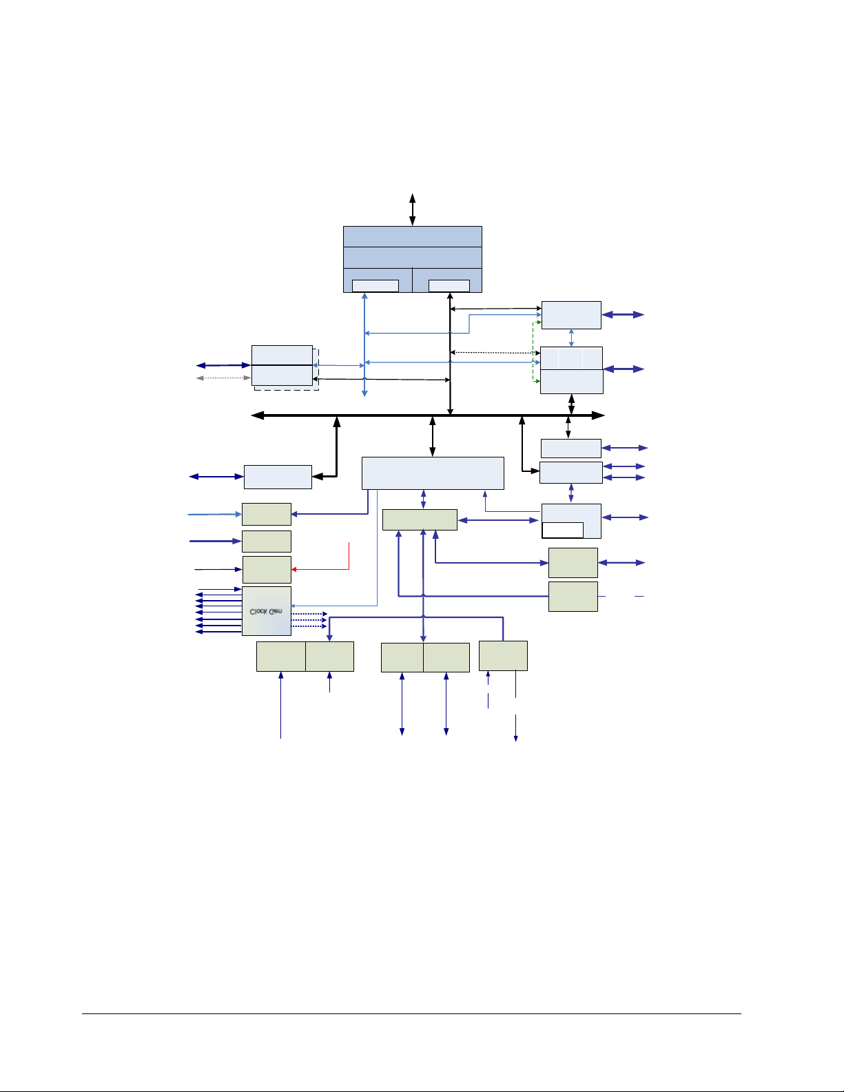
1.3 Block Diagram
This section contains a diagram for the SP5100. Figure 1 below shows the SP5100 internal PCI devices and the major
function blocks.
Figure 1 SP5100 PCI Internal Devices and Major Function Blocks
2012 Advanced Micro Devices, Inc. Block Diagram
AMD SP5100 Register Reference Guide Page 8

©
LPC
PCI Bridge
Bus 0 DEV 20 Function 4
Device ID 4384h
SMBUS /ACPI
Bus 0 DEV 20 Function 0
AB
HD Audio
PORT 1 PORT 0
USB:OHCI(x5)
Bus 0 Dev 18 Function 0,1
Bus 0 Dev 19 Function 0,1
Bus 0 Dev 20 Function 5
Device ID 4397h : 4398h : 4399h
USB:EHCI(x2)
A-LINK
B-LINK
12 USB2.0 + 2
USB1.1 PORTS
6 PCI SLOTS
LPC bus
SPI bus
Debug port
B-LINK A-LINK
Alink Express II
IMC
8051
EC_INT
Flash Controller
(not supported)
SATA Controller
IDE
HD Link
Bus 0 DEV 20 Function 1
Bus 0 DEV 20 Function 2
Bus 0 DEV 17 Function 0
Device ID 4380h
Device ID 438Ch
Device ID 438Dh
Bus 0 DEV 20 Function 3
Device ID 4383h
Device ID 4385h
Device ID 4380h
Device ID 4380h
Device ID 4380h
Bus 0 Dev 18 Function 2
Bus 0 Dev 19 Function 2
Device ID 4396h
2 Register Descriptions: PCI Devices
Note: The SP5100 internal PCI devices are listed in Figur e 2 below. The sub-sections that f ollow provide descriptions of
the PCI configuration space, the I/O space, and the memory space registers for each device. PCI configuration space
registers are only accessible with configuration read or configuratio n write cycles and with the target device selected by
settling its corresponding IDSEL bit in the configuration cycle address field.
2012 Advanced Micro Devices, Inc. Block Diagram
AMD SP5100 Register Reference Guide Page 9
Figure 2: SP5100 PCI Internal Devices

©
Register Name
Offset Address
Vendor ID
00h
Device ID
02h
Command
04h
Status
06h
Revision ID/Class Code
08h
Cache Link Size
0Ch
Master Latency Timer
0Dh
Header Type
0Eh
BIST Mode Type
0Fh
Base Address 0
10h
Base Address 1
14h
Base Address 2
18h
Base Address 3
1Ch
Bus Master Interface Base Address
20h
AHCI Base Address
24h
Subsystem ID and Subsystem Vendor ID
2Ch
Capabilities Pointer
34h
Interrupt Line
3Ch
Interrupt Pin
3Dh
Min_gnt
3Eh
Max_latency
3Fh
Misc control
40h
Watch Dog Control And Status
44h
Watch Dog Counter
46h
Blink Control
48h
MSI Control
50h
MSI Address
54h
MSI Upper Address
58h
MSI Data
5Ch
Power Management Capability ID
60h
Power Management Capability
62h
Power Management Control And Status
64h
Serial ATA Capability Register 0
70h
Serial ATA Capability Register 1
74h
2.1 SATA Registers (Bus 0, Device 17, Function 0)
SATA registers are composed of PCI Config, Memory mapped I/O and I/O space registers. These registers are cleared
by the PCIRST# signal; therefore, they will be cleared on a warm boot.
Note: Some SATA functions are controlled by, and associated with, certain PCI configuration registers in the
SMBus/ACPI device. For more information refer to section 2.4: SMBus Module and ACPI Block (Device 20, Function 0).
The diagram below lists these SATA functions and the associated registers.
2.1.1 PCI Configuration Registers
These registers are accessible only when the SATA controller detects a Configuration Read or Write operation,
with its IDSEL asserted, on the 32-bit PCI bus.
2012 Advanced Micro Devices, Inc. SATA Registers (Bus 0, Device 17, Function 0)
AMD SP5100 Register Reference Guide Page 10

©
Register Name
Offset Address
IDP Index
78h
IDP Data
7Ch
PHY Test In
80h
PHY Test Out
82h
PHY Mode
84h
PHY Global Control
86h
PHY Port0 Control
88h
PHY Port1 Control
8Ch
PHY Port2 Control
90h
PHY Port3 Control
94h
PHY Port4 Control
98h
PHY Port5 Control
9Ch
PHY Port0 GENII Control
A0h
PHY Port1 GENII Control
A2h
PHY Port2 GENII Control
A4h
PHY Port3 GENII Control
A6h
PHY Port4 GENII Control
A8h
PHY Port5 GENII Control
AAh
Port0 BIST Error Count
ACh
Port0 BIST Control/Status
B0h
Reserved
B2h
Port1 BIST Error Count
B4h
Port1BIST Control/Status
B8h
Reserved
BAh
Port2 BIST Error Count
BCh
Port2 BIST Control/Status
C0h
Reserved
C2h
Port3 BIST Error Count
C4h
Port3 BIST Control/Status
C8h
Reserved
CAh
Port4 BIST Error Count
CCh
Port4 BIST Control/Status
D0h
Reserved
D2h
Port5 BIST Error Count
D4h
Port5 BIST Control/Status
D8h
Reserved
DAh
BIST pattern Count
DCh
PCI Target Control TimeOut Counter
E0h
T-Mode BIST Transit Pattern DW1
E4h
T-Mode BIST Transit Pattern DW2
E8h
BIST Transmit Pattern Definition
ECh
Reserved
EE-EFh
20-BIT BIST Transmit Pattern
F0
Reserved
F3h-FFh
Vendor ID - R - 16 bits - [PCI_Reg:00h]
Field Name
Bits
Default
Description
Vendor ID
15:0
1002h
This register holds a unique 16-bit value assigned to a vendor.
And combined with the device ID, it identifies any PCI device.
2012 Advanced Micro Devices, Inc. SATA Registers (Bus 0, Device 17, Function 0)
AMD SP5100 Register Reference Guide Page 11

©
Device ID - R - 16 bits - [PCI_Reg:02h]
Field Name
Bits
Default
Description
Device ID
15:0
4390h
This register holds a unique 16-bit value assigned to a device.
0x40[24] must be programmed to 1’b0 (default).
Mode
Device ID
Sub-Class Code
PCI_CFG 0x40[24]
IDE
4390h
01h
0
AHCI 1
4391h
06h
0
RAID 0, 1, 10 3
4392h
04h
0
AHCI 2
4394h
06h
1
Note 1: For Microsoft inbox AHCI driver support
Note 3: RAID driver support (from third party. AMD does not provide RAID driver)
Command - RW - 16 bits - [PCI_Reg:04h]
Field Name
Bits
Default
Description
I/O Access Enable
0
0b
This bit controls access to the I/O space registers. When this
space access.
memory space access
Bus Master Enable
2
0b
Bus master function enable.
0: Disable.
Recognition Enable
Hard-wired to ‘0’ indicates that there is no specia l suppor t .
Memory Write and
4
0b
Read Only.
command is not supported.
need to snoop VGA palette cycles.
PERR- Detection Enable
6
0b
If set to 1, the IDE host controller asserts PERR- when it is the
not asserted if this bit is 0.
lines.
When used with the combination of base class and sub-class,
the correct functionality of the SATA mode will be enabled by
hardware and software.
Note: To make Device ID 4394h, software will program an
unlock bit (PCI_CFG 0x40[24]) to 1’b1. Once programmed,
Device ID becomes read-only. This bit supersedes the
bonding option and the writing of the Device ID field. That is t o
say, in order to make Device ID 4390h or 4391h, PCI_CFG
Note: The SP5100 SATA controller supports multiple Device IDs to accommodate different SATA configurations.
The following configurations are supported through BIOS programming:
• IDE (IDE emulation mode)
• AHCI mo de
• RAID 0 / RAI D 1 and RAID 10
The SP5100 Device IDs and sub-class codes are assigned as follows:
Note 2: For AMD inbox AHCI driver support (Recommended)
Memory Access Enable 1 0b This bit controls access to the memory space registers. When
Special Cycle
Invalidate Enable
VGA Palette Snoop
Enable
Wait Cycle Enable 7 0b Read Only.
3 0b Read Only.
5 0b Read Only.
bit is 1, it enables SATA controller to response to PCI IO
this bit is 1, it enables SATA controller to response to PCI
1: Enable
Hard-wired to ‘0’ indicates that memory write and invalidate
Hard-wired to ‘0’ indicates the SATA host controller does not
agent receiving data AND it detects a parity error. PERR- is
Hard-wired to ‘0’ indicates the SATA controller does not need
to insert a wait state between the address and data on the AD
2012 Advanced Micro Devices, Inc. SATA Registers (Bus 0, Device 17, Function 0)
AMD SP5100 Register Reference Guide Page 12

©
Command - RW - 16 bits - [PCI_Reg:04h]
Field Name
Bits
Default
Description
SERR- Enable
8
0b
If set to 1 and bit 6 is set, the SATA controller asserts SERRif this bit is 0.
agent are allowed only.
Interrupt Disable
10
0b
(Complies to PCI 2.3 spec.)
Reserved
15:11
00h
Reserved.
Reset Condition: PCI Reset, or Power Management State transition from D3 to D0.
Status - RW - 16 bits - [PCI_Reg:06h]
Field Name
Bits
Default
Description
Reserved
2:0
0h
Reserved.
Interrupt Status
3
0b
Interrupt status bit. It complies with the PCI 2.3 specification.
Capabilities List
4
1b
Read Only.
at 34h.
66MHz Support
5
1b
66MHz capable. This feature is supported in the SATA
controller.
Reserved
6
0b
Reserved.
Fast Back-to-Back
Capable
7
0b
Read Only.
Hard-wired to ‘0’ indicates that Fast Back-to-Back incapable.
Data Parity Error
8
0b
Data Parity reported. Set to 1 if the SATA controller detects
was driven by SATA controller or not.) Write ‘1’ clears this bit.
DEVSEL- Timing
10:9
01b
Read only.
bits are encoded as 01b.
Signaled Target Abort
11
0b
Signaled Target Abort. This bit is set to 1, when the SATA
controller signals Target Abort. Write ‘1’ clears this bit.
Received Target Abort
12
0b
Received Target Abort. This bit is set to 1 when the SATA
master) is aborted by a PCI target. Cleared by writing a 1 to it.
Received Master Abort
13
0b
Received Master Abort Status. Set to 1 when the SATA
detects a PCI address parity error. Write ‘1’ clears this bit.
Detected Parity Error
15
0b
Detected Parity Error. This bit is set to 1 when the SATA
controller detects a parity error. Write ‘1’ clears this bit.
Bit [15:8] are read/write. However, writes “1” will clear these bits.
Revision ID/Class Code- R - 32 bits - [PCI_Reg:08h]
Field Name
Bits
Default
Description
Revision ID
7:0
00h
These bits are default to 00h to indicate the revision level of
when it detects an address parity error. SERR- is not asserted
Fast Back-to-Back
Enable
9 0b Read Only.
Hard-wired to ‘0’ indicates that fast back to back to the same
Default to 1 to indicate that the Capabilities Pointer is located
PERR- asserted while acting as PCI master (whether PERR-
These bits indicate DEVSEL- timing when performing a
positive decode.
Since DEVSEL- is asserted to meet the medium timing, these
controller generated PCI cycle (SATA controller is the PCI
Status
SERR- Status 14 0b SERR- status. This bit is set to 1 when the SATA controller
Reset Condition: PCI Reset, or Power Management State transition from D3 to D0.
controller acting as a PCI master, aborts a PCI bus memory
cycle. Cleared by writing a 1 to this bit. Write ‘1’ clears this bit.
the chip design.
2012 Advanced Micro Devices, Inc. SATA Registers (Bus 0, Device 17, Function 0)
AMD SP5100 Register Reference Guide Page 13

©
Revision ID/Class Code- R - 32 bits - [PCI_Reg:08h]
Field Name
Bits
Default
Description
Operating Mode
15:8
8Fh
RW
See *Note 1
Sub-Class Code
23:16
01h
Sub-Class Code. 01h to indicate an IDE Controller. See *Note
2.
Class Code
31:24
01h
Class Code. These 8 bits are read only and wired to 01h to
*Note 1: Bits [15:8] are writable when PCI_REG 40h[0] is 1. In IDE mode (sub class code ==01) bits [11:8] are
Reset Condition: PCI Reset.
Cache Line Size - RW - 8 b its - [PCI_Reg:0Ch]
Field Name
Bits
Default
Description
Reserved
3:0
0h
Reserved
Cache Line Size Register
7:4
0h
If the value is 1, cache line size is 16 DW (64 byte).
Reset Condition: PCI Reset, or Power Management State transition from D3 to D0.
Master Latency Timer - RW - 8 bits - [PCI_Reg:0Dh]
Field Name
Bits
Default
Description
Reserved
2:0
0h
Reserved
Master Latency Timer
7:3
00h
Master Latency Timer. This number in units of PCICLKs
controller for burst transactions.
Reset Condition: PCI Reset, or Power Management State transition from D3 to D0.
Header Type - R - 8 bits - [PCI_Reg:0Eh]
Field Name
Bits
Default
Description
ASIC Revision A12.
BIST Mode Type - RW - 8 bits - [PCI_Reg:0Fh]
Field Name
Bits
Default
Description
Completion Code
3:0
0h
Read Only.
value indicates a failure.
Selection
writable when PCI_REG 40h[0] ==0.
*Note 2: This field is only write-able when PCI_Reg:40h[0] is set.
Sub-Class Code Program Interface: Controller Type
01 8F IDE
06 01 AHCI
04 00 RAID
Programmable I/F.
Bit [15]: Master IDE Device. Always 1.
Bits [14:12]: Reserved. Always read as 0’s.
Bit [11]: Programmable indicator for Secondary. Always 1 to
indicate that both modes are supported.
Bit [10]: Operating Mode for Secondary.
1: Native PCI-mode.
0: Compatibility Mode
Bit [9]: Programmable indicator for Primary. Always 1 to
indicate that both modes are supported.
Bit [8]: Operating Mode for Primary.
1: Native PCI-mode.
0: Compatibility mode
indicate a Mass-Storage Controller.
represents the guaranteed time slice allowed to IDE host
Header Type 7:0 00h Header Type. Since the IDE host controller is a single-function
device, this register contains a value of 00h. Bit [7] is writable
when PCI configuration register 40h[0] is set. This appli es to
Indicates the completion code status of BIST. A non-zero
2012 Advanced Micro Devices, Inc. SATA Registers (Bus 0, Device 17, Function 0)
AMD SP5100 Register Reference Guide Page 14

©
BIST Mode Type - RW - 8 bits - [PCI_Reg:0Fh]
Field Name
Bits
Default
Description
Reserved
5:4
0h
Reserved
Start BIST
6
0b
Since bit [7] is 0, programming this bit takes no effect.
BIST Capable
7
0
Read Only.
Hard-wired to ‘0’ Indicates no HBA related BIST function
Reset Condition: PCI Reset, or Power Management State transition from D3 to D0.
Note: This does not indicate SATA BIST capability
Base Address 0 - RW - 32 bits - [PCI_Reg:10h]
Field Name
Bits
Default
Description
Resource Type Indicator
0
1b
RTE (Resource Type Indicator). This bit is wired to 1 to
space.
Reserved
2:1
0h
Reserved.
Primary IDE CS0 Base
31:3
0000_
register is
in compatibility mode.
Reset Condition: PCI Reset, or Power Management State transition from D3 to D0.
Base Address 1 - RW - 32 bits - [PCI_Reg:14h]
Field Name
Bits
Default
Description
Resource Type Indicator
0
1b
RTE (Resource Type Indicator). This bit is wired to 1 to
space.
Reserved
1
0b
Reserved.
compatibility mode.
Reset Condition: PCI Reset, or Power Management State transition from D3 to D0.
Base Address 2 - RW - 32 bits - [PCI_Reg:18h]
Field Name
Bits
Defaul
t
Description
Resource Type Indicator
0
1b
RTE (Resource Type Indicator). This bit is wired to 1 to
Reserved
2:1
0h
Reserved.
Secondary IDE CS0
address
31:3
0000_
Under IDE mode, this serves as the base Address for
flash controller, bits [16:3] are read-only.
Reset Condition: PCI Reset, or Power Management State transition from D3 to D0.
Base Address 3 - RW - 32 bits - [PCI_Reg:1Ch]
Field Name
Bits
Default
Description
space.
Reserved
1
0b
Reserved.
Address
Primary IDE CS1 Base
Address
0000h
31:2 0000_
0000h
indicate that the base address field in this register maps to I/O
Base Address for Primary IDE Bus CS0. This
used for native mode only. Base Address 0 is not used
indicate that the base address field in this register maps to I/O
Base Address for Primary IDE Bus CS1. This register is used
for native mode only. Base Address 1 is not used in
indicate that the base address field in this register maps to I/O
space for IDE mode.
When flash controller is enabled (PM_Reg_59, bit 1), this bit is
'0' to indicate that the base address field in this register maps
to memory space.
Base Address
or
Flash Controller base
(See Note)
0000h
Secondary IDE Bus CS0. This register is used for native mode
only. Base Address 2 is not used in compatibility mode.
When flash controller is enabled (PM_Reg_59, bit 1), this
register serves as the base address for the flash controller
Note: When this register serves as the base address for the
Resource Type Indicator 0 1b RTE (Resource Type Indicator). This bit is wired to 1 to
indicate that the base address field in this register maps to I/O
2012 Advanced Micro Devices, Inc. SATA Registers (Bus 0, Device 17, Function 0)
AMD SP5100 Register Reference Guide Page 15

©
Base Address 3 - RW - 32 bits - [PCI_Reg:1Ch]
Field Name
Bits
Default
Description
Secondary IDE CS1
31:2
0000_
register is
in compatibility mode.
Reset Condition: PCI Reset, or Power Management State transition from D3 to D0.
Bus Master Interface Base Address - RW - 32 bits - [PCI_Reg:20h]
Field Name
Bits
Default
Description
Resource Type Indicator
0
1b
RTE (Resource Type Indicator). This bit is wired to 1 to
space.
Reserved
3:1
0h
Reserved.
Bus Master Interface
Register Base Address
31:4
000_
0000h
Base Address for Bus Master interface registers and
correspond to AD[15:4].
Reset Condition: PCI Reset, or Power Management State transition from D3 to D0.
AHCI Base Address - RW - 32 bits - [PCI_Reg:24h]
Field Name
Bits
Default
Description
Resource Type Indicator
0
0b
RTE (Resource Type Indicator). This bit is wired to 0 to
indicate a request for register memory space.
Reserved
9:1
000h
Reserved.
AHCI Base Address
31:10
00_0000
h
Base address of register memory space. This represents a
memory space for support of 4 ports.
Reset Condition: PCI Reset, or Power Management State transition from D3 to D0.
Subsystem ID and Subsystem Vendor ID - RW - 32 bits - [PCI_Reg:2Ch]
Field Name
Bits
Default
Description
Subsystem Vendor ID
15:0
0000h
Subsystem Vendor ID. Can only be written once by software.
Subsystem ID
31:16
0000h
Subsystem ID. Can only be written once by software.
Write once and read only.
Reset Condition: PCI Reset.
Capabilities Pointer - R - 8 bits - [PCI_Reg:34h]
Field Name
Bits
Default
Description
Capabilities Pointer
7:0
60h
The first pointer of Capability block.
Interrupt Line - RW - 8 bits - [PCI_Reg:3Ch]
Field Name
Bits
Default
Description
Interrupt Line
7:0
00h
Identifies which input on the interrupt controller the function’s
register) is routed to
Reset Condition: PCI Reset, or Power Management State transition from D3 to D0.
Interrupt Pin - R - 8 bits - [PCI_Reg:3Dh]
Field Name
Bits
Default
Description
Interrupt Pin
7:0
01h
Hardwired to 01h.
Base Address
0000h
Base Address for Secondary IDE Bus CS1. This
used for native mode only. Base Address 3 is not used
indicate that the base address field in this register maps to I/O
PCI interrupt request pin (as specified in its Interrupt Pin
2012 Advanced Micro Devices, Inc. SATA Registers (Bus 0, Device 17, Function 0)
AMD SP5100 Register Reference Guide Page 16

©
Min_gnt - R - 8 bits - [PCI_Reg:3Eh]
Field Name
Bits
Default
Description
Minimu m Grant
7:0
00h
This register specifies the desired settings for how long of a
Hard-wired to 0’s and always read as 0’s.
Max_latency - R - 8 bits - [PCI_Reg:3Fh]
Field Name
Bits
Default
Description
Maximum Latency
7:0
00h
This register specifies the Maximum Latency time required
Hardwired to 0’s and always read as 0’s.
Misc Control - RW - 32 bits - [PCI_Reg:40h]
Field Name
Bits
Default
Description
Subclass code write
0
0b
Once set, Program Interface register (PCI_Reg:09h), Subclass
(PCI_Reg50h[19:17]) can be progr am ma ble.
Disable Dynamic Sata
Memory Power Saving
1
0b
When clear, dynamic power saving function for SATA internal
memory macros will be performed to reduce power consumption.
Enable dynamic Sata
2
0b
When set, dynamic power saving function for SATA core clock
consumption. See Note 1.
Reserved
3
0b
Reserved
SATA partial/slumber modes that are allowed.
Power Saving
Reserved
15:6
000h
Reserved
See Note3.
Disable port1
17
0b
When set, port1 is disabled and port1 clock is shut down.
Disable port2
18
0b
When set, port2 is disabled and port2 clock is shut down.
Disable port3
19
0b
When set, port3 is disabled and port3 clock is shut down.
Disable port4
20
0b
When set, port4 is disabled and port4 clock is shut down.
Disable port5
21
0b
When set, port5 is disabled and port5 clock is shut down.
Reserved
23:22
00b
Reserved
Lock Flash Device ID
24
When set, SATA Device ID will be Read-Only, and has value
values, other than 0x4394h, defined in PCI_CFG 0x00[31:16].
Reserved
28:25
0h
Reserved
Disabling
mode
29
0b
Disabling testing/enhancement mode in SATA. Need to be
Reserved
31:30
00b
Reserved
burst the SATA controller needs. The value specifies a period
of time in units of ¼ microseconds.
Enable
Core Power Saving
Disable Speed up XP
Boot
Enable Dynamic
Interface Clock
before the SATA controller as a bus-master ca n star t an
accesses
code register (PCI_Reg:0Ah), Multiple Message Capable bits
will be performed during partial/slumber mode to reduce power
4 0b When clear, it fastens XP boot up in IDE mode. However, this bit
needs to be set, when enable SATA partial/slumber pow er
function is in IDE mode.
When set, the SATA partial/slumber power function can be
enabled in IDE mode, but the BIOS IO trap is needed to speed
up XP boot-up in IDE mode.
Please refer to BAR5 + offset 12C/1Ac/22C/2AC[11:8] for the
5
0b
When set, dynamic power saving function for SATA internal bus
interface clock will be performed while there is no outstanding
DMA transaction. See Note 2.
Disable port0 16 0b When set, port0 is disabled and port0 clock is shut down.
0b
testing/enhancement
2012 Advanced Micro Devices, Inc. SATA Registers (Bus 0, Device 17, Function 0)
AMD SP5100 Register Reference Guide Page 17
0x4394h.
When cleared, SATA Device ID will be writable according to the
programmed to 1 and recovered after S0 power lost.

©
Misc Control - RW - 32 bits - [PCI_Reg:40h]
Field Name
Bits
Default
Description
Reset Condition: PCI Reset.
Note3: When set, put PHY port0 is disabled, shut down port0 clock at link/transport layer.
Watch Dog Control And Status - RW - 16 bits - [PCI_Reg:44h]
Field Name
Bits
Default
Description
Watchdog Enable
0
0b
Set the bit to enable the watchdog counter for all the PCI down
stream transaction for both SATA and PATA ports.
Watchdog Timeout
1
0b
Watchdog Counter Timeout Status bit. This bit indicates that
Software writes 1 to clear the status
Software writes 1 to clear the status
Reserved
15:3
0000h
Reserved. Still read/write-able.
This register is used from preventing system hang. Reset Condition: PCI Reset, or Power Management State
transition from D3 to D0.
Watch Dog Counter - RW - 16 bits - [PCI_Reg:46h]
Field Name
Bits
Default
Description
Watchdog Counter
7:0
80h
Specifi es the time out retry count for PCI down stream retries.
This value is used for both SATA and PATA ports.
Reserved
15:8
00h
Reserved. Still read/write-able.
This register is used from preventing system hang. Reset Condition: PCI Reset, or Power Management State
transition from D3 to D0.
B-Link Control - RW - 32 bits - [PCI_Reg:48h]
Field Name
Bits
Default
Description
Reserved
23:0
00_
0000h
Reserved. Still read/write-able.
mode
Reserved
31:25
00h
Reserved. Still read/write-able.
Reset Condition: PCI Reset, or Power Management State transition from D3 to D0.
MSI Control - RW- 32 bits - [PCI_Reg:50h]
Field Name
Bits
Default
Description
Capability ID. Indicates this is MSI capability ID.
Capability Next Pointer
15:8
70h
Read-Only.
capability).
Message Signaled
Interrupt Enable
16
0b
MSI Enable
Note1: Bit [2]: To enable dynamic sataclk shut down function. Sataclk will be shut down during partial/slumber
mode. It will automatically wake-up when received new commands from software, or received
COMWAKE/COMINIT from device. This function will be effective when this bit is set also ACPI-PCI_reg ACh[13]
Note2: When set, enable dynamic blink clock shut down. Blink clk will be shut down when there is no outstanding
DMA operation. “BAR4 + offset 0/8h[0] = 1’b1”,or “BAR5 +offset 134/1B4/234/2B4[31:0] = non-zeros” ,or “BAR5
+offset 138/1B8/238/2B8[31:0] = non-zeros” means there is DMA operation on going.
Status
PATA Watchdog Timeout
Status
the watchdog counter has expired for PCI down stream
transaction and the transaction got aborted due to the fact that
the counter has expired.
2 0b PATA Watchdog Counter Timeout Status bit. This bit indicates
that the watchdog counter in a PATA port has expired for PCI
down stream transaction and the transaction got aborted due
to counter has expired.
Disabling
testing/enhancement
24 0b Disabling testing/enhancement mode in SATA. Need to be
programmed to 1 and recovered after S0 power lost.
Capability ID 7:0 05h Read-Only.
Next Pointer (Default to 70h, points to Index Data pair
2012 Advanced Micro Devices, Inc. SATA Registers (Bus 0, Device 17, Function 0)
AMD SP5100 Register Reference Guide Page 18

©
MSI Control - RW- 32 bits - [PCI_Reg:50h]
Field Name
Bits
Default
Description
Multiple Message
Capable
19:17
010b
Multiple Message Capable (MMC).
*Note
Multiple Message Enable
22:20
0h
Multiple Message Enable (MME).
MSI 64-bit Address
23
1b
Read Only
64-bit address supported
Reserved
31:24
00h
Reserved.
Reset Condition: PCI Reset, or Power Management State transition from D3 to D0.
MSI Address - RW- 32 bits - [PCI_Reg:54h]
Field Name
Bits
Default
Description
Reserved
1:0
0h
Reserved.
always DW aligned.
Reset Condition: PCI Reset, or Power Management State transition from D3 to D0.
MSI Upper Address - RW- 32 bits - [PCI_Reg:58h]
Field Name
Bits
Default
Description
and only implemented if MC.C64=1.
MSI Data - RW- 16 bits - [PCI_Reg:5Ch]
Field Name
Bits
Default
Description
MSI Data
15:0
0000h
MSI Data
Reset Condition: PCI Reset, or Power Management State transition from D3 to D0.
Power Management Capability ID – R - 16 bits - [PCI_Reg:60h]
Field Name
Bits
Default
Description
Capability ID
7:0
01h
Capability ID (Default to 01h, indicates that this pointer is a
PCI power management).
Capability Next Pointer
15:8
50h
Next Pointer (hard wired to 50h, points to MSI capability.
Reset Condition: PCI Reset, or Power Management State transition from D3 to D0.
Power Management Capability - R- 16 bits - [PCI_Reg:62h]
Field Name
Bits
Default
Description
Management Specification.
PME Clock (PMEC)
3
0b
Indicates that PCI clock is not required to generate PME#.
Reserved
4
0b
Reserved
Initialization
Hard wire to 1.
in the D3
COLD
state. Hard wire to 000b.
D1_Support
9
0b
The D1 state is not supported.
D2_Support
10
0b
The D2 state is not supported.
PME_Support
15:11
00h
Hard wired to 00h.
MSI Address 31:2 0000_0000h Lower 32 bits of the system specified message address
MSI Upper Address 31:0 0000_0000h
MSI Upper Address:
Upper 32 bits of the system
specified message address. This register is optional
Reset Condition: PCI Reset, or Power Management State transition from D3 to D0.
Version (VS) 2:0 010b
Device Specific
5 1b Indicates whether device-specific initialization is required.
Indicates support for Revision 1.1 of the PCI Power
Aux_Current 8:6 0h Reports the maximum Suspend well current required when
2012 Advanced Micro Devices, Inc. SATA Registers (Bus 0, Device 17, Function 0)
AMD SP5100 Register Reference Guide Page 19

©
PCI Power Management Control And Status - RW- 16 bits - [PCI_Reg:64h]
Field Name
Bits
Default
Description
Power State (PS)
1:0
00b
Reserved
7:2
00h
Reserved
PME Enable (PMEE)
8
0b
Read Only.
Hard-wired to ‘0’ indicates PME disable
Reserved
14:9
00h
Reserved.
PME Status
15
0b
Read Only.
Hard-wired to ‘0’ as PME disable
Reset Condition: PCI Reset.
Serial ATA Capability Register 0 - R- 32 bits - [PCI_Reg:70h]
Field Name
Bits
Default
Description
Capability ID
7:0
12h
Capability ID (hard wired to 12h, indicates that this pointer is a
Serial ATA Capability)
Capability Next Pointer
15:8
00h
Next Pointer. end of list.
Minor Revision
19:16
0h
Minor revision number of the SATA Capability Pointer
implemented.
Major Revision
23:20
1h
Major revision number of the SATA Capability Pointer
implemented.
Reserved
31:24
00h
Reserved
Serial ATA Capability Register 1 - R- 32 bits - [PCI_Reg:74h]
Field Name
Bits
Default
Description
BAR Location
3:0
1111b
Value 1111b Indicates Index-Data pair is implemented in
space.
are located in Dword granularity.
Reserved
31:24
00h
Reserved.
This set of registers when supported is used for the Index-Data Pair mechanism.
IDP Index Register - RW- 32 bits - [PCI_Reg:78h]
Field Name
Bits
Default
Description
Reserved
1:0
0h
Reserved.
IDP Index
9:2
00h
This register selects the Dword offset of the memory mapped
particular implementation.
Reserved
31:10
00_0000
h
Reserved
This set of registers, when supported, is used for the Index-Data Pair mechanism. Reset Condition: PCI Reset, or
This field is used both to determine the current power state
of the HBA and to set a new power state. The values are:
00 – D0 state
11 – D3
The D1 and D2 states are not supported. When in the
D3
state, the configuration space is available, but the
HOT
register memory spaces are not. Additionally, interrupts
are blocked.
HOT
state
This set of registers when supported is used for the Index-Data Pair mechanism.
Dwords directly following SATACR1 in the PCI configuration
BAR Offset 23:4 000h Indicates the offset into the BAR where the Index-Data Pair
AHCI register to be accessed. The IDP Index should be sized
such that it can access the entire ABAR register space for the
Power Management State transition from D3 to D0.
2012 Advanced Micro Devices, Inc. SATA Registers (Bus 0, Device 17, Function 0)
AMD SP5100 Register Reference Guide Page 20

©
IDP Data Register - RW- 32 bits - [PCI_Reg:7Ch]
Field Name
Bits
Default
Description
IDP Data
31:0
F722_FF
This register is a “window” through which data is read or
Index.
PHY Test In - RW- 16 bits - [PCI_Reg:80h]
Field Name
Bits
Default
Description
PHY transmission enable
0
0b
SATA PHY transmisión enable (txen)
PHY transmissio n clock
1
0b
SATA PHY transmisión clock (tbc)
PHY Test Input data
11:2
000h
SATA PHY transmisión data (txd0:9)
Reserved
15:12
0h
Reserved. Still read/write-able.
PHY Test Out - R- 16 bits - [PCI_Reg:82h]
Field Name
Bits
Default
Description
PHY Test Output data
9:0
000h
SATA PHY receiving data (rxd9:0)
PHY receiving clock
10
0b
SATA PHY receiving clock (asicclk)
PHY receiving data valid
11
0b
SATA PHY receiving data valid (rxdvalid)
valid
Reserved
15:13
0h
Reserved. Still read/write-able.
PHY MODE- RW - 16 bits - [PCI_Reg:84h]
Field Name
Bits
Default
Description
OSCDISABLE
0
0b
Set to ‘1’ to disable PHY Crystal
SATA PHY Enable
1
1b
If set, PHY is enabled.
PHY Global ResetB
2
1b
Active low bit, clear the bit to reset all 4 ports logic in PHY.
Port0 Reset
3
0b
Set the bit to reset PHY port0 logic.
Port1 Reset
4
0b
Set the bit to reset PHY port1 logic.
Port2 Reset
5
0b
Set the bit to reset PHY port2 logic.
Port3 Reset
6
0b
Set the bit to reset PHY port3 logic.
Port4 Reset
7
0b
Set the bit to reset PHY port4 logic.
Port5 Reset
8
0b
Set the bit to reset PHY port5 logic.
Output of PHY, indicates PHY is in test mode.
Reserved
15:10
00h
Reserved. Still read/write-able.
Reset Condition: PCI Reset, or Power Management State transition from D3 to D0.
PHY Global Register - RW- 16 bits - [PCI_Reg:86h]
Field Name
Bits
Default
Description
PHY Global Control
15:0
2C40h
PHY global fine-tune register.
Bit[4] has no effect, actual logia in sata_core (refmode)
85h
All register accesses to IDP Data are Dword granularity.
written to the memory mapped register pointed to by the IDP
Index register. Note that a physical register is not actually
implemented as the data is actually stored in the memory
mapped registers.
Since this is not a physical register, the “default” value is the
same as the default value of the register pointed to by IDP
Reset Condition: PCI Reset, or Power Management State transition from D3 to D0.
PHY receiving signal
12 0b SATA PHY receiving signal valid (sglvalid)
TESTMODE 9 0b Read Only
Bit[6] = EXTCLKEN=1’b1, enables the 100MHz Diff Clock.
Default enabled.
Bit[15] has no effect, actual control in sata_cor e (clk sel)
Reset Condition: PCI Reset.
2012 Advanced Micro Devices, Inc. SATA Registers (Bus 0, Device 17, Function 0)
AMD SP5100 Register Reference Guide Page 21

©
PHY Port0 Register - RW- 32 bits - [PCI_Reg:88h]
Field Name
Bits
Default
Description
TX main driver swing
4:0
10100b
Port0 Tx driving swing[4:0] is valid only at SATA 1.5G if
Note: This applies to all the ASIC Revisions A11 and above.
TX pre-emphasis driver
7:5
000b
Port0 Tx driving swing[7:5] is valid only at SATA 1.5G if
Port0 PHY fine-tune
register
12:8
00h
PHY port0 fine-tune register.
TX pre-emphasis enable
13
0b
Turn on TX pre-emphasis output
0: Disable pre-emphasis
Port0 PHY fine-tune
register
23:14
2d0h
PHY port0 fine-tune register.
Port0 3G Tune Enable
24
1b
When set, 3G PHY will have dedicated fine-tune value,
specified in reg A0h.
Reserved
31:25
00h
Reserved. Still read/write-able.
Reset Condition: PCI Reset.
bit[24]=1. It sets TX main driver swing. The user can program
the optimum value for each SATA port.
Bit 4 Bit 3 Bit 2 Bit 1 Bit 0 Nominal Output
1 0 0 0 0 400mv
1 0 0 1 0 450mv
1 0 1 0 0 500mv
1 0 1 1 0 550mv
1 1 0 0 0 600mv
1 1 0 1 0 650mv
1 1 1 0 0 700mv
1 1 1 1 0 750mv
swing
bit[24]=1. It sets TX pre-emphasis driver swing. The user can
program the optimum pre-emphasis value for each SATA port if
TX pre-emphasis enable bit turned on (bit[13]).
Bit 7 Bit 6 Bit 5 pre-emphasis amount
0 0 0 0mv
0 0 1 25mv
0 1 0 50mv
0 1 1 75mv
1 0 0 100mv
1 0 1 125mv
1 1 0 150mv
1 1 1 175mv
Note: This applies to all the ASIC Revisions A11 and above.
1: Enable pre-emphasis
2012 Advanced Micro Devices, Inc. SATA Registers (Bus 0, Device 17, Function 0)
AMD SP5100 Register Reference Guide Page 22

©
PHY Port1 Register - RW- 32 bits - [PCI_Reg:8Ch]
Field Name
Bits
Default
Description
TX main swing
4:0
10100b
Port1 Tx driving swing[4:0] is valid only at SATA 1.5G if
Note: This applies to all the ASIC Revisions A11 and above.
TX pre-emphasis driver
7:5
000b
Port1 Tx driving swing[7:5] is valid only at SATA 1.5G if
Note: This applies to all the ASIC Revisions A11 and above.
register
0: Disable pre-emphasis
Port1 PHY fine-tune
register
23:14
2d0h
PHY port1 fine-tune register.
specified in reg A2h.
Reserved
31:25
00h
Reserved. Still read/write-able.
bit[24]=1. It sets TX main driver swing. The user can program
the optimum value for each SATA port
Bit 4 Bit 3 Bit 2 Bit 1 Bit 0 Nominal Output
1 0 0 0 0 400mv
1 0 0 1 0 450mv
1 0 1 0 0 500mv
1 0 1 1 0 550mv
1 1 0 0 0 600mv
1 1 0 1 0 650mv
1 1 1 0 0 700mv
1 1 1 1 0 750mv
swing
Port1 PHY fine-tune
TX pre-emphasis enable 13 0b Turn on port1 TX pre-emphasis output
Port1 3G Tune Enable 24 1b When set, 3G PHY will have dedicated fine-tune value,
Reset Condition: PCI Reset.
12:8 00h PHY port1 fine-tune register.
bit[24]=1. It sets TX pre-emphasis driver swing. The user can
program the optimum pre-emphasis value for each SATA port
if TX pre-emphasis enable bit turned on (bit[13]).
Bit 7 Bit 6 Bit 5 pre-emphasis amount
0 0 0 0mv
0 0 1 25mv
0 1 0 50mv
0 1 1 75mv
1 0 0 100mv
1 0 1 125mv
1 1 0 150mv
1 1 1 175mv
1: Enable pre-emphasis
2012 Advanced Micro Devices, Inc. SATA Registers (Bus 0, Device 17, Function 0)
AMD SP5100 Register Reference Guide Page 23

©
PHY Port2 Register - RW- 32 bits - [PCI_Reg:90h]
Field Name
Bits
Default
Description
TX main swing
4:0
10100b
Port2 Tx driving swing[4:0] is valid only at SATA 1.5G if
Note: This applies to all the ASIC Revisions A11 and above.
TX pre-emphasis driver
7:5
000b
Port2 Tx driving swing[7:5] is valid only at SATA 1.5G if
Note: This applies to all the ASIC Revisions A11 and above.
register
0: Disable pre-emphasis
Port2 PHY fine-tune
register
23:14
2d0h
PHY port2 fine-tune register.
specified in reg A4h.
Reserved
31:25
00h
Reserved.
bit[24]=1. It sets TX main driver swing. The user can program
the optimum value for each SATA port.
Bit 4 Bit 3 Bit 2 Bit 1 Bit 0 Nominal Output
1 0 0 0 0 400mv
1 0 0 1 0 450mv
1 0 1 0 0 500mv
1 0 1 1 0 550mv
1 1 0 1 0 600mv
1 1 0 1 0 650mv
1 1 1 0 0 700mv
1 1 1 1 0 750mv
swing
Port2 PHY fine-tune
TX pre-emphasis enable 13 0b Turn on port2 TX pre-emphasis output
Port2 3G Tune Enable 24 1b When set, 3G PHY will have dedicated fine-tune value,
Reset Condition: PCI Reset.
12:8 00h PHY port2 fine-tune register.
bit[24]=1. It sets TX pre-emphasis driver swing. The user can
program the optimum pre-emphasis value for each SATA port
if TX pre-emphasis enable bit turned on (bit[13]).
Bit 7 Bit 6 Bit 5 pre-emphasis amount
0 0 0 0mv
0 0 1 25mv
0 1 0 50mv
0 1 1 75mv
1 0 0 100mv
1 0 1 125mv
1 1 0 150mv
1 1 1 175mv
1: Enable pre-emphasis
2012 Advanced Micro Devices, Inc. SATA Registers (Bus 0, Device 17, Function 0)
AMD SP5100 Register Reference Guide Page 24

©
PHY Port3 Register - RW- 32 bits - [PCI_Reg:94h]
Field Name
Bits
Default
Description
TX main swing
4:0
10100b
Port3 Tx driving swing[4:0] is valid only at SATA 1.5G if
Note: This applies to all the ASIC Revisions A11 and above.
TX pre-emphasis driver
7:5
000b
Port3 Tx driving swing[7:5] is valid only at SATA 1.5G if
Note: This applies to all the ASIC Revisions A11 and above.
register
0: Disable pre-emphasis
Port3 PHY fine-tune
register
23:14
2d0h
PHY port3 fine-tune register.
specified in reg A6h.
Reserved
31:25
00h
Reserved.
bit[24]=1. It sets TX main driver swing. The user can program
the optimum value for each SATA port.
Bit 4 Bit 3 Bit 2 Bit 1 Bit 0 Nominal Output
1 0 0 0 0 400mv
1 0 0 1 0 450mv
1 0 1 0 0 500mv
1 0 1 1 0 550mv
1 1 0 0 0 600mv
1 1 0 1 0 650mv
1 1 1 0 0 700mv
1 1 1 1 0 750mv
swing
Port3 PHY fine-tune
TX pre-emphasis enable 13 0b Turn on port3 TX pre-emphasis output
Port3 3G Tune Enable 24 1b When set, 3G PHY will have dedicated fine-tune value,
Reset Condition: PCI Reset.
12:8 00h PHY port3 fine-tune register.
bit[24]=1. It sets TX pre-emphasis driver swing. The user can
program the optimum pre-emphasis value for each SATA port
if TX pre-emphasis enable bit turned on (bit[13]).
Bit 7 Bit 6 Bit 5 pre-emphasis amount
0 0 0 0mv
0 0 1 25mv
0 1 0 50mv
0 1 1 75mv
1 0 0 100mv
1 0 1 125mv
1 1 0 150mv
1 1 1 175mv
1: Enable pre-emphasis
2012 Advanced Micro Devices, Inc. SATA Registers (Bus 0, Device 17, Function 0)
AMD SP5100 Register Reference Guide Page 25

©
PHY Port4 Register - RW- 32 bits - [PCI_Reg:98h]
Field Name
Bits
Default
Description
TX main swing
4:0
10100b
Port4 Tx driving swing[4:0] is valid only at SATA 1.5G if
Note: This applies to all the ASIC Revisions A11 and above.
TX pre-emphasis driver
7:5
000b
Port4 Tx driving swing[7:5] is valid only at SATA 1.5G if
Note: This applies to all the ASIC Revisions A11 and above.
register
0: Disable pre-emphasis
Port4 PHY fine-tune
register
23:14
2d0h
PHY port4 fine-tune register.
specified in reg A8h.
Reserved
31:25
00h
Reserved.
bit[24]=1. It sets TX main driver swing. The user can program
the optimum value for each SATA port.
Bit 4 Bit 3 Bit 2 Bit 1 Bit 0 Nominal Output
1 0 0 0 0 400mv
1 0 0 1 0 450mv
1 0 1 0 0 500mv
1 0 1 1 0 550mv
1 1 0 0 0 600mv
1 1 0 1 0 650mv
1 1 1 0 0 700mv
1 1 1 1 0 750mv
swing
Port4 PHY fine-tune
TX pre-emphasis enable 13 0b Turn on port4 TX pre-emphasis output
Port4 3G Tune Enable 24 1b When set, 3G PHY will have dedicated fine-tune value,
Reset Condition: PCI Reset.
12:8 00h PHY port4 fine-tune register.
bit[24]=1. It sets TX pre-emphasis driver swing. The user can
program the optimum pre-emphasis value for each SATA port
if TX pre-emphasis enable bit turned on (bit[13]).
Bit 7 Bit 6 Bit 5 pre-emphasis amount
0 0 0 0mv
0 0 1 25mv
0 1 0 50mv
0 1 1 75mv
1 0 0 100mv
1 0 1 125mv
1 1 0 150mv
1 1 1 175mv
1: Enable pre-emphasis
2012 Advanced Micro Devices, Inc. SATA Registers (Bus 0, Device 17, Function 0)
AMD SP5100 Register Reference Guide Page 26

©
PHY Port5 Register - RW- 32 bits - [PCI_Reg:9Ch]
Field Name
Bits
Default
Description
TX main swing
4:0
10100b
Port5 Tx driving swing[4:0] is valid only at SATA 1.5G if
Note: This applies to all the ASIC Revisions A11 and above.
TX pre-emphasis driver
7:5
000b
Port5 Tx driving swing[7:5] is valid only at SATA 1.5G if
Note: This applies to all the ASIC Revisions A11 and above.
register
0: Disable pre-emphasis
Port5 PHY fine-tune
register
23:14
2d0h
PHY port5 fine-tune register.
specified in reg AAh.
Reserved
31:25
00h
Reserved.
bit[24]=1. It sets TX main driver swing. The user can program
the optimum value for each SATA port.
Bit 4 Bit 3 Bit 2 Bit 1 Bit 0 Nominal Output
1 0 0 0 0 400mv
1 0 0 1 0 450mv
1 0 1 0 0 500mv
1 0 1 1 0 550mv
1 1 0 0 0 600mv
1 1 0 1 0 650mv
1 1 1 0 0 700mv
1 1 1 1 0 750mv
swing
Port5 PHY fine-tune
TX pre-emphasis enable 13 0b Turn on port5 TX pre-emphasis output
Port5 3G Tune Enable 24 1b When set, 3G PHY will have dedicated fine-tune value,
Reset Condition: PCI Reset.
12:8 00h PHY port5 fine-tune register.
bit[24]=1. It sets TX pre-emphasis driver swing. The user can
program the optimum pre-emphasis value for each SATA port
if TX pre-emphasis enable bit turned on (bit[13]).
Bit 7 Bit 6 Bit 5 pre-emphasis amount
0 0 0 0mv
0 0 1 25mv
0 1 0 50mv
0 1 1 75mv
1 0 0 100mv
1 0 1 125mv
1 1 0 150mv
1 1 1 175mv
1: Enable pre-emphasis
2012 Advanced Micro Devices, Inc. SATA Registers (Bus 0, Device 17, Function 0)
AMD SP5100 Register Reference Guide Page 27

©
PHY Port0 GENII Register - RW- 16 bits - [PCI_Reg:A0h]
Field Name
Bits
Default
Description
TX main swing
4:0
10100b
Port0 Tx driving swing[4:0] is valid only at SATA 3.0G. It sets
Note: This applies to all the ASIC Revisions A11 and above.
TX pre-emphasis driver
7:5
000b
Port0 Tx driving swing[7:5] is valid only at SATA 3.0G. It sets
Note: This applies to all the ASIC Revisions A11 and above.
register
0: Disable pre-emphasis
Port0 PHY fine-tune
register
15:14
0h
PHY port0 fine-tune register.
PHY Port1 GENII Register - RW- 16 bits - [PCI_Reg:A2h]
Field Name
Bits
Default
Description
TX main swing
4:0
10100b
Port1 Tx driving swing[4:0] is valid only at SATA 3.0G. It sets
Note: This applies to all the ASIC Revisions A11 and above.
TX main driver swing. The user can program the optimum
value for each SATA port.
Bit 4 Bit 3 Bit 2 Bit 1 Bit 0 Nominal Output
1 0 0 0 0 400mv
1 0 0 1 0 450mv
1 0 1 0 0 500mv
1 0 1 1 0 550mv
1 1 0 0 0 600mv
1 1 0 1 0 650mv
1 1 1 0 0 700mv
1 1 1 1 0 750mv
swing
Port0 PHY fine-tune
TX pre-emphasis enable 13 0b Turn on port0 SATA 3.0G TX pre-emphasis output
Reset Condition: PCI Reset.
12:8 00h PHY port0 fine-tune register.
TX pre-emphasis driver swing. The user can program the
optimum pre-emphasis value for each SATA port if TX preemphasis enable bit turned on (bit[13]).
Bit 7 Bit 6 Bit 5 pre-emphasis amount
0 0 0 0mv
0 0 1 25mv
0 1 0 50mv
0 1 1 75mv
1 0 0 100mv
1 0 1 125mv
1 1 0 150mv
1 1 1 175mv
1: Enable pre-emphasis
2012 Advanced Micro Devices, Inc. SATA Registers (Bus 0, Device 17, Function 0)
AMD SP5100 Register Reference Guide Page 28
TX main driver swing. The user can program the optimum
value for each SATA port.
Bit 4 Bit 3 Bit 2 Bit 1 Bit 0 Nominal Output
1 0 0 0 0 400mv
1 0 0 1 0 450mv
1 0 1 0 0 500mv
1 0 1 1 0 550mv
1 1 0 0 0 600mv
1 1 0 1 0 650mv
1 1 1 0 0 700mv
1 1 1 1 0 750mv

©
PHY Port1 GENII Register - RW- 16 bits - [PCI_Reg:A2h]
Field Name
Bits
Default
Description
TX pre-emphasis driver
7:5
000b
Port1 Tx driving swing[7:5] is valid only at SATA 3.0G. It sets
Note: This applies to all the ASIC Revisions A11 and above.
register
0: Disable pre-emphasis
Port1 PHY fine-tune
register
15:14
0h
PHY port1 fine-tune register.
PHY Port2 GENII Register - RW- 16 bits - [PCI_Reg:A4h]
Field Name
Bits
Default
Description
TX main swing
4:0
10100b
Port2 Tx driving swing[4:0] is valid only at SATA 3.0G. It sets
Note: This applies to all the ASIC Revisions A11 and above.
TX pre-emphasis driver
7:5
000b
Port2 Tx driving swing[7:5] is valid only at SATA 3.0G. It sets
Note: This applies to all the ASIC Revisions A11 and above.
swing
Port1 PHY fine-tune
TX pre-emphasis enable 13 0b Turn on port1 SATA 3.0G TX pre-emphasis output
Reset Condition: PCI Reset.
12:8 00h PHY port1 fine-tune register.
TX pre-emphasis driver swing. The user can program the
optimum pre-emphasis value for each SATA port if TX preemphasis enable bit turned on (bit[13]).
Bit 7 Bit 6 Bit 5 pre-emphasis amount
0 0 0 0mv
0 0 1 25mv
0 1 0 50mv
0 1 1 75mv
1 0 0 100mv
1 0 1 125mv
1 1 0 150mv
1 1 1 175mv
1: Enable pre-emphasis
swing
TX main driver swing. The user can program the optimum
value for each SATA port.
Bit 4 Bit 3 Bit 2 Bit 1 Bit 0 Nominal Output
1 0 0 0 0 400mv
1 0 0 1 0 450mv
1 0 1 0 0 500mv
1 0 1 1 0 550mv
1 1 0 0 0 600mv
1 1 0 1 0 650mv
1 1 1 0 0 700mv
1 1 1 1 0 750mv
TX pre-emphasis driver swing. The user can program the
optimum pre-emphasis value for each SATA port if TX preemphasis enable bit turned on (bit[13]).
Bit 7 Bit 6 Bit 5 pre-emphasis amount
0 0 0 0mv
0 0 1 25mv
0 1 0 50mv
0 1 1 75mv
1 0 0 100mv
1 0 1 125mv
1 1 0 150mv
1 1 1 175mv
2012 Advanced Micro Devices, Inc. SATA Registers (Bus 0, Device 17, Function 0)
AMD SP5100 Register Reference Guide Page 29

©
PHY Port2 GENII Register - RW- 16 bits - [PCI_Reg:A4h]
Field Name
Bits
Default
Description
Port2 PHY fine-tune
register
12:8
00h
PHY port2 fine-tune register.
TX pre-emphasis enable
13
0b
Turn on port2 SATA 3.0G TX pre-emphasis output
0: Disable pre-emphasis
Port2 PHY fine-tune
register
15:14
0h
PHY port2 fine-tune register.
Reset Condition: PCI Reset.
PHY Port3 GENII Register - RW- 16 bits - [PCI_Reg:A6h]
Field Name
Bits
Default
Description
TX main swing
4:0
10100b
Port3 Tx driving swing[4:0] is valid only at SATA 3.0G. It sets
Note: This applies to all the ASIC Revisions A11 and above.
TX pre-emphasis driver
7:5
000b
Port3 Tx driving swing[7:5] is valid only at SATA 3.0G. It sets
Note: This applies to all the ASIC Revisions A11 and above.
Port3 PHY fine-tune
register
12:8
00h
PHY port3 fine-tune register.
TX pre-emphasis enable
13
0b
Turn on port3 SATA 3.0G TX pre-emphasis output
0: Disable pre-emphasis
Port3 PHY fine-tune
register
15:14
0h
PHY port3 fine-tune register.
Reset Condition: PCI Reset.
1: Enable pre-emphasis
TX main driver swing. The user can program the optimum
value for each SATA port.
Bit 4 Bit 3 Bit 2 Bit 1 Bit 0 Nominal Output
1 0 0 0 0 400mv
1 0 0 1 0 450mv
1 0 1 0 0 500mv
1 0 1 1 0 550mv
1 1 0 0 0 600mv
1 1 0 1 0 650mv
1 1 1 0 0 700mv
1 1 1 1 0 750mv
swing
TX pre-emphasis driver swing. The user can program the
optimum pre-emphasis value for each SATA port if TX preemphasis enable bit turned on (bit[13]).
Bit 7 Bit 6 Bit 5 pre-emphasis amount
0 0 0 0mv
0 0 1 25mv
0 1 0 50mv
0 1 1 75mv
1 0 0 100mv
1 0 1 125mv
1 1 0 150mv
1 1 1 175mv
1: Enable pre-emphasis
2012 Advanced Micro Devices, Inc. SATA Registers (Bus 0, Device 17, Function 0)
AMD SP5100 Register Reference Guide Page 30

©
PHY Port4 GENII Register - RW- 16 bits - [PCI_Reg:A8h]
Field Name
Bits
Default
Description
TX main swing
4:0
10100b
Port4 Tx driving swing[4:0] is valid only at SATA 3.0G. It sets
Note: This applies to all the ASIC Revisions A11 and above.
TX pre-emphasis driver
7:5
000b
Port4 Tx driving swing[7:5] is valid only at SATA 3.0G. It sets
Note: This applies to all the ASIC Revisions A11 and above.
register
0: Disable pre-emphasis
Port4 PHY fine-tune
register
15:14
0h
PHY port4 fine-tune register.
PHY Port5 GENII Register - RW- 16 bits - [PCI_Reg:AAh]
Field Name
Bits
Default
Description
TX main swing
4:0
10100b
Port5 Tx driving swing[4:0] is valid only at SATA 3.0G. It sets
Note: This applies to all the ASIC Revisions A11 and above.
TX main driver swing. The user can program the optimum
value for each SATA port.
Bit 4 Bit 3 Bit 2 Bit 1 Bit 0 Nominal Output
1 0 0 0 0 400mv
1 0 0 1 0 450mv
1 0 1 0 0 500mv
1 0 1 1 0 550mv
1 1 0 0 0 600mv
1 1 0 1 0 650mv
1 1 1 0 0 700mv
1 1 1 1 0 750mv
swing
Port4 PHY fine-tune
TX pre-emphasis enable 13 0b Turn on port4 SATA 3.0G TX pre-emphasis output
Reset Condition: PCI Reset.
12:8 00h PHY port4 fine-tune register.
TX pre-emphasis driver swing. The user can program the
optimum pre-emphasis value for each SATA port if TX preemphasis enable bit turned on (bit[13]).
Bit 7 Bit 6 Bit 5 pre-emphasis amount
0 0 0 0mv
0 0 1 25mv
0 1 0 50mv
0 1 1 75mv
1 0 0 100mv
1 0 1 125mv
1 1 0 150mv
1 1 1 175mv
1: Enable pre-emphasis
2012 Advanced Micro Devices, Inc. SATA Registers (Bus 0, Device 17, Function 0)
AMD SP5100 Register Reference Guide Page 31
TX main driver swing. The user can program the optimum
value for each SATA port.
Bit 4 Bit 3 Bit 2 Bit 1 Bit 0 Nominal Output
1 0 0 0 0 400mv
1 0 0 1 0 450mv
1 0 1 0 0 500mv
1 0 1 1 0 550mv
1 1 0 0 0 600mv
1 1 0 1 0 650mv
1 1 1 0 0 700mv
1 1 1 1 0 750mv

©
PHY Port5 GENII Register - RW- 16 bits - [PCI_Reg:AAh]
Field Name
Bits
Default
Description
TX pre-emphasis driver
7:5
000b
Port5 Tx driving swing[7:5] is valid only at SATA 3.0G. It sets
Note: This applies to all the ASIC Revisions A11 and above.
register
0: Disable pre-emphasis
Port5 PHY fine-tune
register
15:14
0h
PHY port5 fine-tune register.
Port0 BIST Error Count - R – 32 bits - [PCI_Reg:ACh]
Field Name
Bits
Default
Description
Port0 BIST Error Counter
31:0
0000_
0000h
When reach FFFFFFFFh, the counter value will stay at
FFFFFFFFh.
Reset Condition: PCI Reset, or Power Management State transition from D3 to D0, or BIST Error Count Reset.
Port0 BIST Control/Status - RW - 16 bits - [PCI_Reg:B0h]
Field Name
Bits
Default
Description
Port0 Link BIST Enable
0
0b
Once set, put port0 into Link BIST mode, override normal
operation.
Port0 Link BIST Speed
1
0b
PHY Port0 speed control for Link BIST mode. When set,
GENII is used. If reset, GENI is used.
(0xE8).
Port0 Error Count Reset
6
0b
When set, BIST error counter and Link BIST Done are reset.
latency.
swing
Port5 PHY fine-tune
TX pre-emphasis enable 13 0b Turn on port5 SATA 3.0G TX pre-emphasis output
Reset Condition: PCI Reset.
12:8 00h PHY port5 fine-tune register.
TX pre-emphasis driver swing. The user can program the
optimum pre-emphasis value for each SATA port if TX preemphasis enable bit turned on (bit[13]).
Bit 7 Bit 6 Bit 5 pre-emphasis amount
0 0 0 0mv
0 0 1 25mv
0 1 0 50mv
0 1 1 75mv
1 0 0 100mv
1 0 1 125mv
1 1 0 150mv
1 1 1 175mv
1: Enable pre-emphasis
Port0 Link BIST pattern 5:2 0000b 0000: Pseudorandom with ALIGN insertion (when Error Count
is used, must choose this patte rn).
0001: D10.2 Highest frequency (for Rx eye diagram
measurement).
0010: SYNC primitive (for Rx eye diagram measurement).
0011: Lone Bit Pattern (LBP)
0100: Mid Frequency Test Pattern (MFTP)
0101: 20 bit data pattern, programmed at PCI_Reg:F0h.
0110: Force Far End Retimed Loop Back Mode in HBA.
0111: T-mode enable. T-mode is defined as “Far end transmit
only mode without Device initiating”. In T-mode, the BIST
pattern that is generated is based on the programming in the
BIST Transmit Pattern Registers DW1 (0xE4) and DW2
This bit needs to be set for 10ms, then negated. 10ms is to
ensure PHY is ready in proper frequency, mode and round trip
2012 Advanced Micro Devices, Inc. SATA Registers (Bus 0, Device 17, Function 0)
AMD SP5100 Register Reference Guide Page 32

©
Port0 BIST Control/Status - RW - 16 bits - [PCI_Reg:B0h]
Field Name
Bits
Default
Description
Port0 BIST Error Count
7
0b
When set, BIST Error Count will stop increment if BIST Error
Done is set.
Port0 BIST Error Count
8
0b
When set, the BIST error counter will hold the current value. It
When clear, it has no affect on BIST error counter.
Error Count Reset.
(IDE Data Port) to initiate BIST active FIS.
COMRESET.
Reserved
15:12
0h
Reserved. Still read/writeable.
Reset Condition: PCI Reset, or Power Management State transition from D3 to D0.
Note: Reset Condition for bit [15:11] is PCI Reset.
Port1 BIST Error Count - R - 32 bits - [PCI_Reg:B4h]
Field Name
Bits
Default
Description
Port1 BIST Error Counter
31:0
0000_
0000h
When reach FFFFFFFFh, the counter value will stay at
FFFFFFFFh.
Reset Condition: PCI Reset, or Power Management State transition from D3 to D0, or BIST Error Count Reset.
Port1 BIST Control/Status - RW - 16 bits - [PCI_Reg:B8h]
Field Name
Bits
Default
Description
Port1 Link BIST Enable
0
0b
Once set, put port1 into Link BIST mode, override normal
operation.
Port1 Link BIST Speed
1
0b
PHY Port1 speed control for Link BIST mode. When set,
GENII is used. If reset, GENI is used.
Port1 Link BIST pattern
5:2
0000b
0000: Pseudorandom with ALIGN insertion (when Error Count
(0xE8).
Port1 Error Count Reset
6
0b
When set, BIST error counter and Link BIST Done are reset.
latency.
Done is set.
Freeze Mode
Hold
Port0 BIST Done 9 0b Read Only
Port0 SATA BIST Enable 10 0b Enable SATA BIST Vendor Mode: for using AR0/BAR2 offset0
Port0 BIST with
disconnect Enable
11 0b When set and a BIST Activate FIS is received from the device,
Count Hold is set.
When reset, BIST Error Count will stop increment if Link BIST
won’t be increased even on the event of mis-comparison.
When set, means BIST has verified x amount patterns
specified in the BIST pattern Count. Will be reset by BIST
the HBA will ignore all OOB signaling from the device . The
HBA can exit this mode either thru a hardware reset or a
software initiated COMRESET.
Note: This bit will not be cleared from a software initiated
is used, must choose this patte rn).
0001: D10.2 Highest frequency (for Rx eye diagram
measurement).
0010: SYNC primitive (for Rx eye diagram measurement).
0011: Lone Bit Pattern (LBP)
0100: Mid Frequency Test Pattern (MFTP)
0101: 20 bit data pattern, programmed at PCI_Reg:F0h.
0110: Force Far End Retimed Loop Back Mode in HBA.
0111: T-mode enable. T-mode is defined as “Far end transmit
only mode without Device initiating”. In T-mode, the BIST
pattern that is generated is based on the programming in the
BIST Transmit Pattern Registers DW1 (0xE4) and DW2
This bit needs to be set for 10ms, then negated. 10ms is to
ensure PHY is ready in proper frequency, mode and round trip
Port1 BIST Error Count
Freeze Mode
7 0b When set, BIST Error Count will stop increment if BIST Error
Count Hold is set.
When reset, BIST Error Count will stop increment if Link BIST
2012 Advanced Micro Devices, Inc. SATA Registers (Bus 0, Device 17, Funct ion 0)
AMD SP5100 Register Reference Guide Page 33

©
Port1 BIST Control/Status - RW - 16 bits - [PCI_Reg:B8h]
Field Name
Bits
Default
Description
Port1 BIST Error Count
8
0b
When set, the BIST error counter will hold the current value. It
When clear, it has no affect on BIST error counter.
Error Count Reset.
(IDE Data Port) to initiate BIST active FIS.
COMRESET.
Reserved
15:12
0h
Reserved. Still read/writeable.
Reset Condition: PCI Reset, or Power Management State transition from D3 to D0.
Note: Reset Condition for bit [15:11] is PCI Reset.
Port2 BIST Error Count - R - 32 bits - [PCI_Reg:BCh]
Field Name
Bits
Default
Description
Port2 BIST Error Counter
31:0
0000_
0000h
When reach FFFFFFFFh, the counter value will stay at
FFFFFFFFh.
Reset Condition: PCI Reset, or Power Management State transition from D3 to D0, or BIST Error Count Reset.
Port2 BIST Control/Status - RW - 16 bits - [PCI_Reg:C0h]
Field Name
Bits
Default
Description
Port2 Link BIST Enable
0
0b
Once set, put port2 into Link BIST mode, override normal
operation.
Port2 Link BIST Speed
1
0b
PHY Port2 speed control for Link BIST mode. When set,
GENII is used. If reset, GENI is used.
(0xE8).
Port2 BIST Error Count
6
0b
When set, BIST error counter and Link BIST Done are reset.
latency.
Port2 BIST Error Count
7
0b
When set, Link BIST Error Count will stop increment if Link
BIST Done is set.
Hold
Port1 BIST Done 9 0b Read Only
Port1 SATA BIST Enable 10 0b Enable SATA BIST Vendor Mode: for using AR0/BAR2 offset0
Port1 BIST with
disconnect Enable
11 0b When set and a BIST Activate FIS is received from the device,
won’t be increased even on the event of mis-comparison.
When set, means BIST has verified certain amount patterns
specified in the BIST pattern Count. Will be reset by BIST
the HBA will ignore all OOB signaling from the device. The
HBA can exit this mode either thru a hardware reset or a
software initiated COMRESET.
Note: This bit will not be cleared from a software initiated
Port2 Link BIST pattern 5:2 0000b 0000: Pseudorandom with ALIGN insertion (when Error Count
is used, must choose this patte rn).
0001: D10.2 Highest frequency (for Rx eye diagram
measurement).
0010: SYNC primitive (for Rx eye diagram measurement).
0011: Lone Bit Pattern (LBP)
0100: Mid Frequency Test Pattern (MFTP)
0101: 20 bit data pattern, programmed at PCI_Reg:F0h.
0110: Force Far End Retimed Loop Back Mode in HBA.
0111: T-mode enable. T-mode is defined as “Far end transmit
only mode without Device initiating”. In T-mode, the BIST
pattern that is generated is based on the programming in the
BIST Transmit Pattern Registers DW1 (0xE4) and DW2
Reset
Freeze Mode
Port2 BIST Error Count
Hold
8 0b When set, the BIST error counter will hold the current value. It
This bit needs to be set for 10ms, then negated. 10ms is to
ensure PHY is ready in proper frequency, mode and round trip
BIST Error Count Hold is set.
When reset, Link BIST Error Count will stop increment if Link
won’t be increased even on the event of mis-comparison.
When clear, it has no affect on BIST error counter.
2012 Advanced Micro Devices, Inc. SATA Registers (Bus 0, Device 17, Function 0)
AMD SP5100 Register Reference Guide Page 34

©
Port2 BIST Control/Status - RW - 16 bits - [PCI_Reg:C0h]
Field Name
Bits
Default
Description
Port2 BIST Done
9
0b
Read Only
Error Count Reset.
Port2 SATA BIST Enable
10
0b
Enable SATA BIST Vendor Mode: for using AR0/BAR2 offset0
(IDE Data Port) to initiate BIST active FIS.
Port2 BIST with
11
0b
When set and a BIST Activate FIS is received from the device,
COMRESET.
Reserved
15:12
0h
Reserved. Still read/writeable.
Note: Reset Condition for bit [15:12] is PCI Reset.
Port3 BIST Error Count - R - 32 bits - [PCI_Reg:C4h]
Field Name
Bits
Default
Description
0000h
FFFFFFFFh.
Reset Condition: PCI Reset, or Power Management State transition from D3 to D0, or BIST Error Count Reset.
Port3 BIST Control/Status - RW - 16 bits - [PCI_Reg:C8h]
Field Name
Bits
Default
Description
operation.
Port3 Link BIST Speed
1
0b
PHY Port3 speed control for Link BIST mode. When set,
GENII is used. If reset, GENI is used.
Port3 Link BIST pattern
5:2
0000b
0000: Pseudorandom with ALIGN insertion (when Error Count
(0xE8).
Port3 BIST Error Count
6
0b
When set, BIST error counter and Link BIST Done are reset.
Port3 BIST Error Count
7
0b
When set, BIST Error Count will stop increment if BIST Error
is set.
Port3 BIST Error Count
8
0b
When set, the BIST error counter will hold the current value. It
When clear, it has no affect on BIST error counter.
Error Count Reset.
When set, means BIST has verified certain amount patterns
specified in the BIST pattern Count. Will be reset by BIST
disconnect Enable
Reset Condition: PCI Reset, or Power Management State transition from D3 to D0.
the HBA will ignore all OOB signaling from the device. The
HBA can exit this mode either thru a hardware reset or a
software initiated COMRESET.
Note: This bit will not be cleared from a software initiated
Port3 BIST Error Counter 31:0 0000_
When reach FFFFFFFFh, the counter value will stay at
Port3 Link BIST Enable 0 0b Once set, put port3 into Link BIST mode, override normal
is used, must choose this patte rn).
0001: D10.2 Highest frequency (for Rx eye diagram
measurement).
0010: SYNC primitive (for Rx eye diagram measurement).
0011: Lone Bit Pattern (LBP)
0100: Mid Frequency Test Pattern (MFTP)
0101: 20 bit data pattern, programmed at PCI_Reg:F0h.
0110: Force Far End Retimed Loop Back Mode in HBA.
0111: T-mode enable. T-mode is defined as “Far end transmit
only mode without Device initiating”. In T-mode, the BIST
pattern that is generated is based on the programming in the
BIST Transmit Pattern Registers DW1 (0xE4) and DW2
Reset
Freeze Mode
Hold
Port3 BIST Done 9 0b Read Only
2012 Advanced Micro Devices, Inc. SATA Registers (Bus 0, Device 17, Function 0)
AMD SP5100 Register Reference Guide Page 35
This bit needs to be set for 10ms, then negated. 10ms is to
ensure PHY is ready in proper frequency, mode and round trip
latency.
Count Hold is set.
When reset, BIST Error Count will stop increment if BIST Done
won’t be increased even on the event of mis-comparison.
When set, means BIST has verified certain amount patterns
specified in the BIST pattern Count. Will be reset by BIST

©
Port3 BIST Control/Status - RW - 16 bits - [PCI_Reg:C8h]
Field Name
Bits
Default
Description
Port3 SATA BIST Enable
10
0b
Enable SATA BIST Vendor Mode: for using AR0/BAR2 offset0
(IDE Data Port) to initiate BIST active FIS.
Port3 BIST with
11
0b
When set and a BIST Activate FIS is received from the device,
COMRESET.
Reserved
15:12
0h
Reserved. Still read/writeable.
Note: Reset Condition for bit [15:12] is PCI Reset.
Port4 BIST Error Count - R - 32 bits - [PCI_Reg:CCh]
Field Name
Bits
Default
Description
0000h
FFFFFFFFh.
Reset Condition: PCI Reset, or Power Management State transition from D3 to D0, or BIST Error Count Reset.
Port4 BIST Control/Status - RW - 16 bits - [PCI_Reg:D0h]
Field Name
Bits
Default
Description
operation.
Port4 Link BIST Speed
1
0b
PHY Port4 speed control for Link BIST mode. When set,
GENII is used. If reset, GENI is used.
Port4 Link BIST pattern
5:2
0000b
0000: Pseudorandom with ALIGN insertion (when Error Count
(0xE8).
latency.
Port4 BIST Error Count
7
0b
When set, BIST Error Count will stop increment if BIST Error
Port4 BIST Error Count
8
0b
When set, the BIST error counter will hold the current value. It
When clear, it has no affect on BIST error counter.
Port4 BIST Done
9
0b
Read Only
Error Count Reset.
(IDE Data Port) to initiate BIST active FIS.
disconnect Enable
Reset Condition: PCI Reset, or Power Management State transition from D3 to D0.
the HBA will ignore all OOB signaling from the device. The
HBA can exit this mode either thru a hardware reset or a
software initiated COMRESET.
Note: This bit will not be cleared from a software initiated
Port4 BIST Error Counter 31:0 0000_
When reach FFFFFFFFh, the counter value will stay at
Port4 Link BIST Enable 0 0b Once set, put port4 into Link BIST mode, override normal
is used, must choose this patte rn).
0001: D10.2 Highest frequency (for Rx eye diagram
measurement).
0010: SYNC primitive (for Rx eye diagram measurement).
0011: Lone Bit Pattern (LBP)
0100: Mid Frequency Test Pattern (MFTP)
0101: 20 bit data pattern, programmed at PCI_Reg:F0h.
0110: Force Far End Retimed Loop Back Mode in HBA.
0111: T-mode enable. T-mode is defined as “Far end transmit
only mode without Device initiating”. In T-mode, the BIST
pattern that is generated is based on the programming in the
BIST Transmit Pattern Registers DW1 (0xE4) and DW2
Port4 BIST Error Count
Reset
Freeze Mode
Hold
Port4 SATA BIST Enable 10 0b Enable SATA BIST Vendor Mode: for using AR0/BAR2 offset0
2012 Advanced Micro Devices, Inc. SATA Registers (Bus 0, Device 17, Function 0)
AMD SP5100 Register Reference Guide Page 36
6 0b When set, BIST error counter and Link BIST Done are reset.
This bit needs to be set for 10ms, then negated. 10ms is to
ensure PHY is ready in proper frequency, mode and round trip
Count Hold is set.
When reset, BIST Error Count will stop increment if BIST Done
is set.
won’t be increased even on the event of mis-comparison.
When set, means BIST has verified certain amount patterns
specified in the BIST pattern Count. Will be reset by BIST

©
Port4 BIST Control/Status - RW - 16 bits - [PCI_Reg:D0h]
Field Name
Bits
Default
Description
Port4 BIST with
11
0b
When set and a BIST Activate FIS is received from the device,
COMRESET.
Reserved
15:12
0h
Reserved. Still read/writeable.
Note: Reset Condition for bit [15:12] is PCI Reset.
Port5 BIST Error Count - R - 32 bits - [PCI_Reg:D4h]
Field Name
Bits
Default
Description
0000h
FFFFFFFFh.
Reset Condition: PCI Reset, or Power Management State transition from D3 to D0, or BIST Error Count Reset.
Port5 BIST Control/Status - RW - 16 bits - [PCI_Reg:D8h]
Field Name
Bits
Default
Description
operation.
GENII is used. If reset, GENI is used.
Port5 Link BIST pattern
5:2
0000b
0000: Pseudorandom with ALIGN insertion (when Error Count
(0xE8).
Port5 BIST Error Count
6
0b
When set, BIST error counter and Link BIST Done are reset.
latency.
Port5 BIST Error Count
7
0b
When set, BIST Error Count will stop increment if BIST Error
is set.
Port5 BIST Error Count
8
0b
When set, the BIST error counter will hold the current value. It
When clear, it has no affect on BIST error counter.
Error Count Reset.
(IDE Data Port) to initiate BIST active FIS.
disconnect Enable
Reset Condition: PCI Reset, or Power Management State transition from D3 to D0.
the HBA will ignore all OOB signaling from the device. The
HBA can exit this mode either thru a hardware reset or a
software initiated COMRESET.
Note: This bit will not be cleared from a software initiated
Port5 BIST Error Counter 31:0 0000_
When reach FFFFFFFFh, the counter value will stay at
Port5 Link BIST Enable 0 0b Once set, put port5 into Link BIST mode, and ov erride normal
Port5 Link BIST Speed 1 0b PHY Port5 speed control for Link BIST mode. When set,
is used, must choose this patte rn).
0001: D10.2 Highest frequency (for Rx eye diagram
measurement).
0010: SYNC primitive (for Rx eye diagram measurement).
0011: Lone Bit Pattern (LBP)
0100: Mid Frequency Test Pattern (MFTP)
0101: 20 bit data pattern, programmed at PCI_Reg:F0h.
0110: Force Far End Retimed Loop Back Mode in HBA.
0111: T-mode enable. T-mode is defined as “Far end transmit
only mode without Device initiating”. In T-mode, the BIST
pattern that is generated is based on the programming in the
BIST Transmit Pattern Registers DW1 (0xE4) and DW2
Reset
Freeze Mode
Hold
Port5 BIST Done 9 0b Read Only
Port5 SATA BIST Enable 10 0b Enable SATA BIST Vendor Mode: for using AR0/BAR2 offset0
2012 Advanced Micro Devices, Inc. SATA Registers (Bus 0, Device 17, Function 0)
AMD SP5100 Register Reference Guide Page 37
This bit needs to be set for 10ms, then negated. 10ms is to
ensure PHY is ready in proper frequency, mode and round trip
Count Hold is set.
When reset, BIST Error Count will stop increment if BIST Done
won’t be increased even on the event of mis-comparison.
When set, means BIST has verified certain amount patterns
specified in the BIST pattern Count. Will be reset by BIST

©
Port5 BIST Control/Status - RW - 16 bits - [PCI_Reg:D8h]
Field Name
Bits
Default
Description
Port5 BIST with
11
0b
When set and a BIST Activate FIS is received from the device,
COMRESET.
Reserved
15:12
0h
Reserved. Still read/writeable.
Note: Reset Condition for bit [15:12] is PCI Reset.
BIST Pattern Count - RW - 32 bits - [PCI_Reg:DCh]
Field Name
Bits
Default
Description
This register is used for both SATA BIST and Link BIST.
Reset Condition: PCI Reset, or Power Management State transition from D3 to D0.
PCI Target Control TimeOut- RW - 16 bits - [PCI_Reg:E0h]
Field Name
Bits
Default
Description
PCI Target Control
7:0
80h
This register is used for programming the PCI Target Control
The counter will be disabled if the count is programmed to 0x0.
Reserved
15:8
00h
Reserved.
Reset Condition: PCI Reset, or Power Management State transition from D3 to D0.
T-Mode BIST Transit Pattern DW1 - RW - 32 bits - [PCI_Reg:E4h]
Field Name
Bits
Default
Description
Reset Condition: PCI Reset, or Power Management State transition from D3 to D0
T-Mode BIST Transit Pattern DW2 - RW - 32 bits - [PCI_Reg:E8h]
Field Name
Bits
Default
Description
T-mode BIST Transit
31:0
0000_
Transit Patterns DW2
Reset Condition: PCI Reset, or Power Management State transition from D3 to D0
BIST Transit Pattern Definition- RW - 16 bits - [PCI_Reg:ECh]
Field Name
Bits
Default
Description
T-mode A bit
0
0b
ALIGN primitive bypass mode
T-mode S bit
1
0b
Scrambling Bypass.
T-mode P bit
2
0b
The transmit primitives bit.
0000h
Reset Condition: PCI Reset, or Power Management State transition from D3 to D0
disconnect Enable
Reset Condition: PCI Reset, or Power Management State transition from D3 to D0.
the HBA will ignore all OOB signaling from the device. The
HBA can exit this mode either thru a hardware reset or a
software initiated COMRESET.
Note: This bit will not be cleared from a software initiated
BIST Pattern Count 31:0 0000_2000h This count specifies how many Octal WORD pattern need
to be checked before BIST Done bit be set. This count
value is used fro all the 4 ports. 400h default value would
be used for tester, which means 32K DWORD pattern
would be compared for BIST test. Value of “0000_0000”h
means the maximum patterns (16,000, 000, 000) checked.
TimeOut Count
TimeOut Count used to clear any stale target commands to
the hosts controller. Granularity is 15.5us (Count * 15.5 us)
T-mode BIST Transit
Pattern DW1
31:0 0000_
0000h
Pattern DW2
0000h
Reserved 31:3 0000_
Transit Patterns DW1
Reserved. Still read/writeable.
2012 Advanced Micro Devices, Inc. SATA Registers (Bus 0, Device 17, Function 0)
AMD SP5100 Register Reference Guide Page 38

©
20-BIT BIST Transit Pattern - RW - 24 bits - [PCI_Reg:F0h]
Field Name
Bits
Default
Description
20-BIT BIST Transit
19:0
0_
20 bit Transit Data Patterns without going through 8b/10b
Reserved
31:20
000h
Reserved. Still read/writable.
Reset Condition: PCI Reset, or Power Management State transition from D3 to D0
Spare Register - RW - 8 bits - [PCI_Reg:F4h]
Field Name
Bits
Default
Description
Reserved
7:0
00h
Reserved. Still read/writable.
Reset Condition: PCI Reset, or Power Management State transition from D3 to D0
Spare Register1 - RW - 32 bits - [PCI_Reg:F8h]
Field Name
Bits
Default
Description
Spare register1
31:0
0000_
0000h
Reserved and can be read/writeable
Reset Condition: PCI Reset, or Power Management State transition from D3 to D0
Spare Register2 - RW - 32 bits - [PCI_Reg:FCh]
Field Name
Bits
Default
Description
0000h
Reset Condition: PCI Reset, or Power Management State transition from D3 to D0
Pattern
Spare register2
31:0 0000_
0000h
encode.
Reserved and can be read/writeable
2012 Advanced Micro Devices, Inc. SATA Registers (Bus 0, Device 17, Function 0)
AMD SP5100 Register Reference Guide Page 39

©
Address (hex)
Name and Function
Compatibilty Mode
Native Mode (Offset)
Read Function
Write Function
IDE Command Block Registers
Primary
Secondary
BAR0/BAR2
1F0
170
(Primary or Secondary)
Base Address 0 + 0
Data (16 bit)
Data (16 bit)
1F1
171
(Primary or Secondary)
Base Address 0 + 1
Error register
Features register
1F2
172
(Primary or Secondary)
Base Address 0 + 2
Sector Count
Sector Count
Base Address + 3
1F4
174
(Primary or Secondary)
Base Address + 4
Cylinder Low
Cylinder Low
1F5
175
(Primary or Secondary)
Base Address + 5
Cylinder High
Cylinder High
Base Address + 6
1F7
177
(Primary or Secondary)
Base Address + 7
Status
Command
IDE Control Block Registers
Primary
Secondary
BAR1/BAR3
3F6
376
(Primary or Secondary)
Base Address + 2
Alternate Status
Device Control
Register Name
Offset Address
[Primary/Secondary]
Bus-master IDE Command
00h/08h
Bus-master IDE Status
02h/0Ah
Descriptor Table Pointer
04h/0Ch
Bus-master IDE Command - RW- 8 bits - [IO_Reg: B AR4 + 00/08h]
Field Name
Bits
Default
Description
be reset by soft ware (device driver).
Reserved
2:1
0h
Reserved.
Bus Master Read/Write
3
0b
Bus Master IDE r/w (direction) control
if terminated by Bus Master IDE stop.
Reserved
7:4
0h
Reserved.
2.1.2 SATA I/O Register for IDE Mode
2.1.2.1 BAR0/BAR2/BAR1/BAR3 Registers
BAR0/BAR2 uses 8 bytes of I/O space. BAR0 is used for Primary channel and BAR2 is used for Secondary channel
during IDE native mode. BAR1/BAR3 uses 2 bytes of I/O space. BAR1 is used for Primary channel and BAR3 is
used for Secondary channel during IDE native mode.
1F3 173 (Primary or Secondary)
1F6 176 (Primary or Secondary)
Sector Number Sector Number
Drive/Head Drive/Head
2.1.2.2 BAR4 Registers
BAR4 uses 16 bytes of I/O space. The Bus-master interface base address register (BAR4) defines the base address
of the IO spare.
Bus Master IDE
Start/Stop
2012 Advanced Micro Devices, Inc. SATA Registers (Bus 0, Device 17, Function 0)
AMD SP5100 Register Reference Guide Page 40
0 0b Bus Master IDE Start (1)/Stop (0).
This bit will not be reset by interrupt from IDE device. This must
0: Memory -> IDE
1: IDE -> Memory
This bit should not change during Bus Master transfer cycle, even

©
Bus-master IDE Status - RW- 8 bits - [IO_Reg: BAR4 + 02/0Ah]
Field Name
Bits
Default
Description
Bus Master Active
0
0b
Bus Master IDE active. This bit is set to 1 when bit 0 in the Bus
IDE command register is set to 0.
Bus Master DMA Error
1
0b
IDE DMA error. This bit is set when the IDE host controller
transferring data on the PCI bus. Write 1 clears this bit.
IDE Interrupt
2
0b
IDE Interrupt. Indicates when an IDE device has asserted its
detected on the interrupt line.
Reserved
4:3
0h
Reserved.
Master Device DMA
Capable
5
0b
Device 0 (Master) DMA capable.
Capable
Simplex only. This bit is hard-wired as 0.
Descriptor Table Pointer - RW- 32 bits - [IO_Reg: BAR4 + 04/0Ch]
Field Name
Bits
Default
Description
Reserved
1:0
0h
Reserved.
Descriptor Table Base
Address
31:2
0000_0000h
Base Address of Descriptor Table. These bits correspond to
Address [31-02].
Register Name
Offset Address
Generic Host Control
00h-23h
Reserved
24h-9Fh
Vendor Specific registers
A0h-FFh
Port 0 port control registers
100h-17Fh
Port 1 port control registers
180h-1FFh
Port 2 port control registers
200h-27Fh
Port 3 port control registers
280h-2FFh
Port 4 port control registers
300h-37Fh
Port 5 port control registers
380h-3FFh
Master IDE command address register is set to 1. The IDE host
controller sets this bit to 0 when the last transfer for a region is
performed. This bit is also set to 0 when bit 0 of the Bus Master
encounters a target abort, master abort, or Parity error while
interrupt line. IRQ14 is used for the Primary channel and IRQ15 is
used for the secondary channel. If the interrupt stat us bit is s et to
0, by writing a 1 to this bit while the interrupt line is still at the
active level, this bit remains 0 until another assertion edge is
Slave Device DMA
Simplex Only 7 0b Read Only.
6 0b Device 1 (Slave) DMA capable.
2.1.3 SATA Memory Mapped Register for AHCI Mode
2.1.3.1 BAR5 Registers
These are the AHCI memory map registers. The base address is defined through ABAR (BAR5) register
2012 Advanced Micro Devices, Inc. SATA Registers (Bus 0, Device 17, Function 0)
AMD SP5100 Register Reference Guide Page 41

©
Register Name
Offset Address
Host Capabilities(CAP)
00h-03h
Global Host Control(GHC)
04h-07h
Interrupt Status(IS)
08h-0Bh
Ports Implemented(PI)
0Ch-0Fh
Version(VS)
10h-13h
Command Completion Coalescing
Control(CCC_CTL)
14h-17h
Command Completion Coalsecing
Ports(CCC_PORTS)
18h-1Bh
Enclosure Management Location(EM_LOC)
1Ch-1Fh
Enclosure Management Control(EM_CTL)
20h-23h
vendor specific
A0h-FFh
HBA Capabilities – R - 32bits [Mem_reg: ABAR + 00h]
Field Name
Bits
Default
Description
Number of Ports
4:0
00101b
0’s based value indicating the maximum number of ports
indicated in the GHC.PI register.
Supports External SATA
5
0b
When set to ‘1’, indicates that the HBA has one or more
accessible.
Enclosure Management
6
0b
When set to ‘1’, indicates that the HBA supports enclosure
and EM_CTL global HBA registers are not implemented.
CCC_PORTS global HBA registers are not implemented.
command slots is available on each implemented port.
2.1.3.2 Generic Host Control
The following registers apply to the entire HBA.
2.1.3.3 Offset 00h: CAP – HBA Capabilities
This register indicates the basic capabilities of the HBA to driver software.
(SXS)
Supported (EMS)
Command Completion
Coalescing Supported
(CCCS)
Number of Command
Slots (NCS)
supported by the HBA silicon. A maximum of 32 ports can be
supported. A value of ‘0h’, indicating one port, is the
minimum requirement. Note that the number of ports
indicated in this field may be more than the number of ports
Serial ATA ports that has a signal only connector that is
externally accessible. If this bit is set to ‘1 ’, softw ar e may
refer to the PxCMD.ESP bit to determine whether a specific
port has its signal connector externally accessible as a signal
only connector (i.e. power is not part of that connector).
When the bit is cleared to ‘0’, indicates that the HBA has no
Serial ATA ports that have a signal only connector externally
management. When enclosure management is supported,
the HBA has implemented the EM_LOC and EM_CTL global
HBA registers. When cleared to ‘0’, indicates that the HBA
does not support enclosure management and the EM_LOC
7 1b When set to ‘1’, indicates that the HBA supports command
completion coalescing. When command comp let ion
coalescing is supported, the HBA has implemented the
CCC_CTL and the CCC_PORTS global HBA registers.
When cleared to ‘0’, indicates that the HBA does not supp or t
command completion coalescing and the CCC_CTL and
12:8 11111b 0’s based value indicating the number of command slot s per
port supported by this HBA. A minimum of 1 and maximum
of 32 slots per port can be supported. The same number of
2012 Advanced Micro Devices, Inc. SATA Registers (Bus 0, Device 17, Function 0)
AMD SP5100 Register Reference Guide Page 42

©
HBA Capabilities – R - 32bits [Mem_reg: ABAR + 00h]
Field Name
Bits
Default
Description
Partial State Capable
13
1b
Indicates whether the HBA can support transitions to the
be supported.
can be supported.
PIO command protocol.
1.0 and 1.1 HBAs shall h av e this bit cle ared to ‘0’.
HBA.
register interface.
have this bit cleared to ‘0’.
set from a previous operation.
(PSC):
Slumber State Capable
(SSC):
PIO Multiple DRQ Block
(PMD)
FIS-based Switching
Supported (FBSS)
Supports Port Multiplier
(SPM)
Partial state. When cleared to ‘0’, software must not allow
the HBA to initiate transitions to the Partial state via agressive
link power management nor the PxCMD.ICC field in each
port, and the PxSCTL.IPM field in each port must be
programmed to disallow device initiated Partial requests.
When set to ‘1’, HBA and device initiated Partial requests can
14 1b Indicates whether the HBA can support transitions to the
Slumber state. When cleared to ‘0’, software must not allow
the HBA to initiate transitions to the Slumber state via
agressive link power management nor the PxCMD.ICC field
in each port, and the PxSCTL.IPM field in each port must be
programmed to disallow device initiated Slumber requests.
When set to ‘1’, HBA and device initiated Slumber requests
15 1b If set to ‘1’, the HBA supports multiple DRQ block data
transfers for the PIO command protocol. If cleared to ‘0’ the
HBA only supports single DRQ block data transfers for the
16 0b When set to ‘1’, indicates that the HBA supports Port
Multiplier FIS-based switching. When cleared to ‘0’, indicates
that the HBA does not support FIS-based switching. AHCI
17 1b Indicates whether the HBA can support a Port Multiplier.
When set, a Port Multiplier using command-bas ed switching
is supported. When cleared to ‘0’, a Port Multiplier is not
supported, and a Port Multiplier may not be attached to this
Supports AHCI mode
only (SAM)
Supports Non-Zero DMA
Offsets (SNZO)
Interface Speed Support
(ISS)
Supports Command List
Override (SCLO)
18 0b The SATA controller may optionally support AHCI access
19 0b When set to ‘1’, indicates that the HBA can support non-zero
23:20 2h
24 1b When set to ‘1’, the HBA supports the PxCMD.CLO bit and its
mechanisms only. A value of '0' indicates that in addition to
the native AHCI mechanism (via ABAR), the SATA controller
implements a legacy, task-file based register interface such
as SFF-8038i. A value of '1' indicates that the SATA
controller does not implement a legacy, task-file based
DMA offsets for DMA Setup FISes. This bit is reserved for
future AHCI enhancements. AHCI 1.0 and 1.1 HBAs shall
Indicates the maximum speed the HBA can support on its
ports. These encodings match the system software
programmable PxSCTL.DET.SPD field. Values are:
Bits Definition
0000 Reserved
0001 Gen 1 (1.5 Gbps)
0010
0011 - 1111 Reserved
associated function. When cleared to ‘0’, the HBA is not
capable of clearing the BSY and DRQ bits in the Status
register in order to issue a software reset if these bits are still
Gen 1 (1.5 Gbps) and Gen 2 (3
Gbps)
2012 Advanced Micro Devices, Inc. SATA Registers (Bus 0, Device 17, Function 0)
AMD SP5100 Register Reference Guide Page 43

©
HBA Capabilities – R - 32bits [Mem_reg: ABAR + 00h]
Field Name
Bits
Default
Description
Supports Activity LED
25
1b
When set to ‘1’, the HBA supports a single activity indication
cleared to ‘0’, this function is not supported.
Supports Aggressive
26
1b
When set to ‘1’, the HBA can support auto-generating link
PxCMD.ASP bits as reserved.
Supports Staggered
27
0b
When set to ‘1’, the HBA supports staggered spin-up on its
BIOS prior to OS initiallization.
Supports Mechanical
28
1b
When set to ‘1’, the HBA supports mechanical presence
loaded by the BIOS prior to OS initialization.
Supports SNotification
29
1b
When set to ‘1’, the
Supports Native
30
1b
Indicates whether the HBA supports Serial ATA native
issue any native command queuing commands.
Supports 64-bit
31
1b
Indicates whether the HBA can access 64-bit data structures.
treated as ‘0’ by the HBA.
(SAL)
Link Power Management
(SALP)
Spin-up (SSS)
Presence Switch (SMPS)
Register (SSNTF)
Command Queuing
(SNCQ)
output pin. This pin can be connected to an LED on the
platform to indicate device activity on any drive. When
requests to the Partial or Slumber states when there are no
commands to process. When cleared to ‘0’, this function is
not supported and software shall treat the PxCMD.ALPE and
ports, for use in balancing power spikes. When cleared to ‘0’,
this function is not supported. This value is loaded by the
switches on its ports for use in hot plug operations. When
cleared to ‘0’, this function is not supported. This value is
HBA supports the PxSNTF (SNotification) regi ster and its
associated functionality. When cleared to ‘0’, the HBA does
not support the PxSNTF (SNotification) register and its
associated functionality.
command queuing. If set to ‘1’, an HBA shall handle DMA
Setup FISes natively, and shall handle the auto-activate
optimization through that FIS. If cleared to ‘0’, native
command queuing is not supported and software should not
Addressing (S64A)
When set to ‘1’, the HBA shall make the 32-bit upper bits of
the port DMA Descriptor, the PRD Base, and each PRD entry
read/write. When cleared to ‘0’, these are read-only and
2012 Advanced Micro Devices, Inc. SATA Registers (Bus 0, Device 17, Function 0)
AMD SP5100 Register Reference Guide Page 44

©
2.1.3.4 Offset 04h: GHC – Global HBA Control
Global HBA Control – RW - 32bits [Mem_reg: ABAR + 04h]
Field Name
Bits
Default
Description
HBA Reset (HR)
0
0b
a description on which bits are reset when this bit is set.
Interrupt Enable (IE)
1
0b
This global bit enables interrupts from the HBA. When
disabled. When set, interrupts are enabled.
and is not “reverting” to that mode. Read Only
Reserved
30:3
000_0000h
Reserved.
This register controls the various global actions of the HBA.
When set by SW, this bit causes an internal reset of the HBA.
All state machines that relate to data transfers and queuing
shall return to an idle condition, and all ports shall be reinitialized via COMRESET (if staggered spin-up is not
supported). If staggered spin-up is supported, then it is the
responsibility of software to spin-up each port after the reset
has completed.
When the HBA has performed the reset action, it shall reset
this bit to ‘0’. A software write of ‘0’ shall have no effect. For
cleared (reset default), all interrupt sources from all ports are
MSI Revert to Single
Message (MRSM)
2 0b
When set to ‘1’ by hardware, indicates that the HBA
requested more than one MSI vector but has reverted to
using the first vector only. When this bit is cleared to ‘0’, the
HBA has not reverted to single MSI mode (i.e. hardware is
already in single MSI mode, software has allocated the
number of messages requested, or hardware is sharing
interrupt vectors if MC.MME < MC.MMC).
The HBA may revert to single MSI mode when the number of
vectors allocated by the host is less than the number
requested. This bit shall only be set to ‘1’ when the following
conditions hold:
• MC.MSIE = ‘1’ (MSI is enabled)
• MC.MMC > 0 (multiple messages requested)
• MC.MME > 0 (more than one message allocated)
• MC.MME != MC.MMC (messages allocated not
equal to number requested)
When this bit is set to ‘1’, single MSI mode operation is in use
and software is responsible for clearing bits in the IS register
to clear interrupts.
This bit shall be cleared to ‘0’ by hardware when any of the
four conditions stated is false. This bit is also cleared to ‘0’
when MC.MSIE = ‘1’ and MC.MME = 0h. In this case, the
hardware has been programmed to use single MSI mode,
2012 Advanced Micro Devices, Inc. SATA Registers (Bus 0, Device 17, Function 0)
AMD SP5100 Register Reference Guide Page 45

©
Global HBA Control – RW - 32bits [Mem_reg: ABAR + 04h]
Field Name
Bits
Default
Description
AHCI Enable (AE)
31
0b
Interrupt Status - RW -32 bits [Mem_reg: ABAR + 08h]
Field Name
Bits
Default
Description
these bits.
Ports Implemented Register - R -32 bits [Mem_reg: ABAR + 0Ch]
Field Name
Bits
Default
Description
to ‘1’.
When set, indicates that communication to the HBA shall be
via AHCI mechanisms. This can be used by an HBA that
supports both legacy mechanisms (such as SFF-80 38i) and
AHCI to know when the HBA is running under an AHCI
driver.
When set, software shall only communicate with the HBA
using AHCI. When cleared, software shall only communicate
with the HBA using legacy mechanisms. When cleared
FISes are not posted to memory and no commands are sent
via AHCI mechanisms.
Software shall set this bit to ‘1’ before accessing other AHCI
registers.
2.1.3.5 Offset 08h: IS – Interrupt Status Register
This register indicates which of the ports within the controller have an interrupt pending and require service.
Interrupt Pending Status
(IPS)
31:0 0000_0000h
If set, indicates that the corresponding port has an interrupt
pending. Software can use this information to determine
which ports require service after an interrupt.
The IPS[x] bit is only defined for ports that are implemented
or for the command completion coalescing interrupt defined
by CCC_CTL.INT. All other bits are reserved. Write 1 clear
2.1.3.6 Offset 0Ch: PI – Ports Implemented
This register indicates which ports are exposed by the HBA. It is loaded by the BIOS. It indicates which ports that the
HBA supports are available for software to use. For example, on an HBA that supports 6 ports as indicated in
CAP.NP, only ports 1 and 3 could be available, with ports 0, 2, 4, and 5 being unavailable. Software must not read or
write to registers within unavailable ports. The intent of this register is to allow system vendors to build platforms that
support less than the full number of ports implemented on the HBA silicon.
Port Implemented (PI) 31:0 0000_000Fh This register is bit significant. If a bit is set to ‘1’, the
corresponding port is available for software to use. If a bit is
cleared to ‘0’, the port is not available for software to use.
The maximum number of bits set to ‘1’ shall not exceed
CAP.NP + 1, although the number of bits set in this register
may be fewer than CAP.NP + 1. At least one bit shall be set
2012 Advanced Micro Devices, Inc. SATA Registers (Bus 0, Device 17, Function 0)
AMD SP5100 Register Reference Guide Page 46

©
AHCI Version- R – 32 bits [M em_reg : AB AR + 10h]
Field Name
Bits
Default
Description
Minor Version Number
(MNR)
15:0
0100h
Indicates the minor version is “10”.
Major Version Number
(MJR)
31:16
0001h
Indicates the major version is “1”
Command Completion Coalescing Contro l(CCC_CTL) - RW – 32bits [Mem_reg: ABAR + 14h]
Field Name
Bits
Default
Description
CCC_CTL Enable
0
0b
When cleared to ‘0’, the command completion coale scing
updated values for the TV and CC fields shall take effect.
Reserved
2:1
0h
Reserved
This field also specifies the interrupt v ector used for MSI.
Command Completions
15:8
01h
Specifies the number of command completions that are
interrupts are only generated based on the timer in this case.
2.1.3.7 Offset 10h: VS – AHCI Version
This register indicates the major and minor version of the AHCI specification that the HBA implementation supports. The
upper two bytes represent the major version number, and the lower two bytes represent the minor version number.
Example: Version 3.12 would be represented as 00030102h. Three versions of the specification are valid: 0.95, 1.0, and
1.1.
2.1.3.8 Offset 14h: CCC_CTL – Command Completion Coalescing Control
The command completion coalescing control register is use d to config ure the com man d co mple tion coale sc ing feat ure
for the entire HBA.
Implementation Note: HBA state variables (examples include hCccComplete and hCccTimer) are used to describe the
required externally visible behavior. Implementations are not required to have internal state values that directly
correspond to these variables.
feature is disabled and no CCC interrupts are generated.
When set to ‘1’, the command completion coalescing feat ur e
is enabled and CCC interrupts may be generated based on
timeout or command completion conditions. Software shall
only change the contents of the TV and CC fields when EN is
cleared to ‘0’. On transition of this bit from ‘0’ to ‘1’, any
CCC Interrupt (INT) 7:3 1Fh Read Only
Specifies the interrupt used by the CCC feature. This
interrupt must be marked as unused in the Ports
Implemented (PI) register by the corresponding bit being set
to ‘0’. Thus, the CCC interrupt corresponds to the interrupt
for an unimplemented port on the controller. When a CCC
interrupt occurs, the IS.IPS[INT] bit shall be asserted to ‘1’.
(CC)
necessary to cause a CCC interrupt. The HBA has an
internal command completion counter, hCccComplete.
hCccComplete is incremented by one each time a selected
port has a command completion. When hCccComplete is
equal to the command completions value, a CCC interrupt is
signaled. The internal command completion counter is reset
to ‘0’ on the assertion of each CCC interrupt. A value of ‘0’
for this field shall disable CCC interrupts being generated
based on the number of commands completed, i.e. CCC
2012 Advanced Micro Devices, Inc. SATA Registers (Bus 0, Device 17, Function 0)
AMD SP5100 Register Reference Guide Page 47

©
Command Completion Coalescing Contro l(CCC_CTL) - RW – 32bits [Mem_reg: ABAR + 14h]
Field Name
Bits
Default
Description
Timeout Value (TV)
31:16
0001h
The timeout value is specified in 1 millisecond intervals. The
of each CCC interrupt. A timeout value of ‘0’ is reserved.
Command Completion Coalescing Ports - RW – 32bits [Mem_reg: ABAR + 18h]
Field Name
Bits
Default
Description
Ports (PRT)
31:0
0000_0000h
This register is bit significant. Each bit corresponds to a
timer increment (1 millisecond).
Register Name
Offset Address
Port-N Command List Base Address(PNCLB)
00h-03h + Port offset
Port-N Command List Base Address Upper 32-
Bits(PNCLBU)
Port-N FIS Base Address Upper 32-Bits(PNFBU)
0Ch-0Fh + Port offset
Port-N Interrupt Status(PNIS)
10h-13h + Port offset
Port-N Interrupt Enable(PNIE)
14h-17h + Port offset
Port-N Command and Status(PNCMD)
18h-1Bh + Port offset
Reserved
1Ch-1Fh + Port offset
Port-N Task File Data(PNTFD)
20h-23h + Port offset
Port-N Signature(PNSIG)
24h-27h + Port offset
Port-N Serial ATA Status (PNSSTS)
28h-2Bh + Port offset
Port-N Serial ATA Control (PNSCTL)
2Ch-2Fh + Port offset
Port-N Serial ATA Error (PNSERR)
30h-33h + Port offset
Port-N Serial ATA Active (PNSACT)
34h-37h + Port offset
Port-N Command Issue(PNCI)
38h-3Bh + Port offset
Port-N SNotification (PNSNTF)
3Ch-3Fh + Port offset
Reserved for FIS-based Switching Definition
40h-43h + Port offset
Reserved
44h-6Fh + Port offset
Port-N Vendor Specific(PNVS)
70h-7Fh + Port offset
*N is the port number, 0 ~ 5
timer accuracy shall be within 5%. hCccTimer is loaded with
this timeout value. hCccTimer is only decremented when
commands are outstanding on selected ports. The HBA will
signal a CCC interrupt when hCccTimer has decremented to
‘0’. hCccTimer is reset to the timeout value on the assertion
2.1.3.9 Offset 18h: CCC_PORTS – Command Completion Coalescing Ports
The command completion coalescing ports register is used to specify the ports that are coalesced as part of the CCC
feature when CCC_CTL.EN = ‘1’.
particular port, where bit 0 corresponds to port 0. If a bit is
set to ‘1’, the corresponding port is part of the command
completion coalescing feature. If a bit is cleared to ‘0’, the
port is not part of the command completion coalescing
feature. Bits set to ‘1’ in this register must also have the
corresponding bit set to ‘1’ in the Ports Implemented register.
An updated value for this field shall take effect within one
Note: Registers at offset A0h to FFh are vendor specific.
2.1.3.10 Port Registers (one set per port)
The following registers describe the registers necessary to implement port 0. Additional ports shall have the same
register mapping. Port 1 starts at 180h, port 2 starts at 200h, port 3 at 280h, etc. The algorithm for software to
determine the offset is as follows:
• Port offset = 100h + (PI Asserted Bit Position * 80h)
04h-07h + Port offset
Port-N FIS Base Address(PNFB) 08h-0Bh + Port offset
2012 Advanced Micro Devices, Inc. SATA Registers (Bus 0, Device 17, Function 0)
AMD SP5100 Register Reference Guide Page 48

©
Port-N Command List Base Address -RW -32 bits [Mem_reg: ABAR + port offset + 00h]
Field Name
Bits
Default
Description
Reserved
9:0
000h
Reserved.
indicated by bits 09:00 being read only.
Port-N Command List Base Upper Address -RW - 32 bits [Mem_reg: ABAR + port offset + 04h]
Field Name
Bits
Default
Description
support 64-bit addressing.
Port–N FIS Base Address -RW -32 bits [Mem_reg: ABAR + port offset + 08h]
Field Name
Bits
Default
Description
Reserved
7:0
00h
Reserved.
bit base physical address for received FISes.
by bits 07:00 being read only.
Port-N FIS Base Address Upper –RW – 32 bits [Mem_reg: ABAR + port offset + 0Ch]
Field Name
Bits
Default
Description
FIS Base Address Upper
31:0
0000_0000h
support 64-bit addressing.
Port–N Interrupt Status - RW - 32 bits [Mem_reg: ABAR + port offset + 10h]
Field Name
Bits
Default
Description
Device to Host Register
FIS Interrupt (DHRS)
0
0b
A D2H Register FIS has been received with the ‘I’ bit set, and
has been copied into system memory.
PIO Setup FIS Interrupt
1
0b
A PIO Setup FIS has been received with the ‘I’ bit set, it has
data transfer resulted in an error.
DMA Setup FIS Interrupt
(DSS)
2
0b
A DMA Setup FIS has been received with the ‘I’ bit set and
has been copied into system memory.
Set Device Bits Interrupt
(SDBS)
3
0b
A Set Device Bits FIS has been received with the ‘I’ bit set
and has been copied into system memory.
Command List Base
Address (CLB)
31:10 00_0000h Indicates the 32-bit base physical address for the command
list for this port. This base is used when fetching commands
to execute. The structure pointed to by this address range is
1K-bytes in length. This address must be 1K-by te alig ned as
Command List Base
Address Upper (CLBU)
31:0 0000_0000h
Indicates the upper 32-bits for the command list base
physical address for this port. This base is used when
fetching commands to execute.
This register shall be read only ‘0’ for HBAs that do not
FIS Base Address (FB): 31:8 00_0000h Indicates the 32-
The structure pointed to by this address ra nge is 256 by tes i n
length. This address must be 256-byte aligned as indicated
(FBU)
Indicates the upper 32-bits for the received FIS base physical
address for this port.
This register shall be read only ‘0’ for HBAs that do not
(PSS)
been copied into system memory, and the data related to that
FIS has been transferred. This bit shall be set even if the
2012 Advanced Micro Devices, Inc. SATA Registers (Bus 0, Device 17, Function 0)
AMD SP5100 Register Reference Guide Page 49

©
Port–N Interrupt Status - RW - 32 bits [Mem_reg: ABAR + port offset + 10h]
Field Name
Bits
Default
Description
Unknown FIS Interrupt
4
0b
Read Only
become out of sync.
Descriptor Processed
5
0b
Port Connect Change
6
0b
Read Onby
PxSERR.DIAG.X is cleared.
to ‘1’.
Reserved
21:8
0000h
Reserved
clear this bit, software must clear P0SERR.DIAG.N to ‘0’.
enumeration is complete on the Port Multiplier.
Overflow Status (OFS)
24
0b
Indicates that the HBA received more bytes from a device
than was specified in the PRD table for the command.
Reserved
25
0b
Reserved
Interface Non-fatal Error
Status (INFS)
26
0b
Indicates that the HBA encountered an error on the Serial
ATA interface but was able to continue operation.
Interface Fatal Error
Status (IFS)
27
0b
Indicates that the HBA encountered an error on the Serial
ATA interface which caused the transfer to stop.
system memory.
Host Bus Fatal Error
29
0b
Indicates that the HBA encountered a host bus error that it
such an indication would be a target or master abort.
(TFES):
device and the error bit (bit 0) is set.
Cold Port Detect Status
31
0b
When set, a device status has changed as detected by the
set to ‘1’.
Write 1 clear these status bits
(UFS)
(DPS)
Status (PCS)
Device Mechanical
Presence Status (DMPS)
PhyRdy Change Status
(PRCS)
Incorrect Port Multiplier
Status (IPMS):
When set to ‘1’, indicates that an unknown FIS was received
and has been copied into system memory. This bit is cleared
to ‘0’ by software clearing the PxSERR.DIAG.F bit to ‘0’.
Note that this bit does not directly reflect the PxSERR.DIAG.F
bit. PxSERR.DIAG.F is set immediately when an unknown
FIS is detected, whereas this bit is set when that FIS is
posted to memory. Software should wait to act on an
unknown FIS until this bit is set to ‘1’ or the two bits may
A PRD with the ‘I’ bit set has transferred all of its data.
1=Change in Current Connect St atus . 0=No change in
Current Connect Status. This bit reflects the state of
PxSERR.DIAG.X. This bit is only cleared when
7 0b When set, indicates that a mechanical presence switch
attached to this port has been opened or closed, which may
lead to a change in the connection state of the device. This
bit is only valid if both CAP.SMPS and P0CMD.MPSP are set
22 0b Read Only
When set to ‘1’ indicates the internal PhyRdy signal changed
state. This bit reflects the state of P0SERR.DIAG.N. To
23 0b Indicates that the HBA received a FIS from a device whose
Port Multiplier field did not match what was expected. The
IPMS bit may be set during enumeration of devices on a Port
Multiplier due to the normal Port Multiplier enumeration
process. It is recommended that IPMS only be used after
Host Bus Data Error
Status (HBDS)
Status (HBFS)
Task File Error Status
(CPDS)
28 0b Indicates that t he HBA encountered a data error
30 0b This bit is set whenever the status register is updated by the
2012 Advanced Micro Devices, Inc. SATA Registers (Bus 0, Device 17, Function 0)
AMD SP5100 Register Reference Guide Page 50
(uncorrectable ECC / parity) when reading from or writing to
cannot recover from, such as a bad software pointer. In PCI,
cold presence detect logic. This bit can either be set due to a
non-connected port receiving a device, or a connected port
having its device removed. This bit is only valid if the port
supports cold presence detect as indicated by PxCMD.CPD

©
Port-N Interrupt Enable - RW -32 bits [Mem_reg: ABAR + port offset + 14h]
Field Name
Bits
Default
Description
Device to Host Register
(DHRE)
0
0b
When set, GHC.IE is set, and P0IS.DHRS is set, the HBA
Enable (PSE)
generate an interrupt.
DMA Setup FIS Interrupt
Enable (DSE)
2
0b
When set, GHC.IE is set, and P0IS.DSS is set, the HBA shall
generate an interrupt.
Set Device Bits FIS
Interrupt Enable (SDBE)
3
0b
When set, GHC.IE is set, and P0IS.SDBS is set, the HBA
shall generate an interrupt.
Unknown FIS Interrupt
Enable (UFE)
4
0b
When set, GHC.IE is set, and P0IS.UFS is set to ‘1’, the HBA
shall generate an interrupt.
Interrupt Enable (DPE)
generate an interrupt.
Enable (PCE)
generate an interrupt.
Device Mechanical
7
0b
switch, this bit shall be a read-only ‘0’.
Reserved
21:8
0000h
Reserved
Enable (PRCE)
set to ‘1’, the HBA shall generate an interrupt.
Incorrect Port Multiplier
Enable (IPME)
23
0b
When set, and GHC.IE and P0IS.IPMS are set, the HBA shall
generate an interupt.
Overflow Enable (OFE)
24
0b
When set, and GHC.IE and P0IS.OFS are set, the HBA shall
generate an interupt.
Reserved
25
0b
Reserved
Interface Non-fatal Error
Enable (INFE)
26
0b
When set, GHC.IE is set, and P0IS.INFS is set, the HBA shall
generate an interrupt.
Interface Fatal Error
Enable (IFE)
27
0b
When set, GHC.IE is set, and P0IS.IFS is set, the HBA shall
generate an interrupt..
Enable (HBDE)
shall generate an interrupt..
Enable (HBFE)
shall generate an interrupt.
Task File Error Enable
(TFEE)
30
0b
When set, GHC.IE is set, and P0S.TFES is set, the HBA shall
generate an interrupt.
Cold Presence Detect
31
0b
shall be a read-only ‘0’.
Port-N Command and Status - R - 32 bits [Mem_reg: ABAR + port offset + 18h]
Field Name
Bits
Default
Description
Start (ST)
0
0b
RW
PxCMD.FRE has been set to ‘1’.
FIS Interrupt Enable
PIO Setup FIS Interrupt
Descriptor Processed
Port Change Interrupt
Presence Enable
(DMPE)
PhyRdy Change Interrupt
shall generate an interrupt.
1 0b When set, GHC.IE is set, and P0IS.PSS is set, the HBA shall
5 0b When set, GHC.IE is set, and P0IS.DPS is set, the HBA shall
6 0b When set, GHC.IE is set, and P0IS.PCS is set, the HBA shall
When set, and GHC.IE is set to ‘1’, and P0IS.DMPS is set,
the HBA shall generate an interrupt.
For systems that do not support a mechanical presence
22 0b When set to ‘1’, and GHC.IE is set to ‘1’, and P0IS.PRCS is
Host Bus Data Error
Host Bus Fatal Error
Enable (CPDE)
28 0b when set, GHC.IE is set, and P0IS.HBDS is set, the HBA
29 0b When set, GHC.IE is set, and P0IS.HBFS is set, the HBA
When set, GHC.IE is set, and P0S.CPDS is set, the HBA
shall generate an interrupt.
For systems that do not support cold presence detect, this bit
When set, the HBA may process the command list. When
cleared, the HBA may not process the command list.
Whenever this bit is changed from a ‘0’ to a ‘1’, the HBA
starts processing the command list at entry ‘0’. Whenever
this bit is changed from a ‘1’ to a ‘0’, the PxCI register is
cleared by the HBA upon the HBA putting the controller into
an idle state. This bit shall only be set to ‘1’ by software after
AMD SP5100 Register Reference Guide Page 51
2012 Advanced Micro Devices, Inc. SATA Registers (Bus 0, Device 17, Function 0)

©
Port-N Command and Status - R - 32 bits [Mem_reg: ABAR + port offset + 18h]
Field Name
Bits
Default
Description
Spin-Up Device (SUD)
1
1b
This bit is read/write for HBAs that support staggered spin-up
‘0’ and PxSCTL.DET=0h, the HBA will enter listen mode.
Power On Device (POD)
2
1b
This bit is read/write for HBAs that support cold presence
cold-presence detectable port.
the BSY and DRQ bits are still set in the PxTFD.STS register.
cleared to ‘0’ before setting PxCMD.ST to ‘1’.
FIS Receive Enable
4
0b
register to be cleared
Reserved
7:5
0h
Reserved
Current Command Slot
12:8
00h
This field is valid when P0CMD.ST is set to ‘1’ and shall be
slot 1.
bit if both CAP.SMPS and P0CMD.MPSP are set to ‘1’.
via CAP.SSS. This bit is read only ‘1’ for HBAs that do not
support staggered spin-up. On an edge detect from ‘0’ to ‘1’,
the HBA shall start a COMRESET initializatoin sequence to
the device. Clearing this bit to ‘0’ does not cause any OOB
signal to be sent on the interface. When this bit is cleared to
detection on this port as indicated by PxCMD.CPD set to ‘1’.
This bit is read only ‘1’ for HBAs that do not support cold
presence detect. When set, the HBA sets the state of a pin
on the HBA to ‘1’ so that it may be used to provide power to a
Command List Override
(CLO)
(FRE)
3 0b
RW
Setting this bit to ‘1’ causes PxTFD.STS.BSY and
PxTFD.STS.DRQ to be cleared to ‘0’. This allows a software
reset to be transmitted to the device regardless of whether
The HBA sets this bit to ‘0’ when PxTFD.STS.BSY and
PxTFD.STS.DRQ have been cleared to ‘0’. A write to this
register with a value of ‘0’ shall have no effect.
This bit shall only be set to ‘1’ immediately prior to setting the
PxCMD.ST bit to ‘1’ from a previous value of ‘0’. Setting this
bit to ‘1’ at any other time is not supported and will result in
indeterminate behavior. Software must wait for CLO to be
When set, the HBA may post received FISes into the FIS
receive area pointed to by PxFB (and for 64-bit HBAs,
PxFBU). When cleared, received FISes are not accepted by
the HBA, except for the first D2H register FIS after the
initialization sequence, and no FISes are posted to the FIS
receive area.
System software must not set this bit until PxFB (PxFBU)
have been programmed with a valid pointer to the FIS receive
area, and if software wishes to move the base, this bit must
first be cleared, and software must wait for the FR bit in this
(CCS)
Mechanical Presence
Switch State (MPSS)
2012 Advanced Micro Devices, Inc. SATA Registers (Bus 0, Device 17, Function 0)
13 1b The MPSS bit reports the state of a mechanical presence
AMD SP5100 Register Reference Guide Page 52
set to the command slot value of the command that is
currently being issued by the HBA. When P0CMD.ST
transitions from ‘1’ to ‘0’, this field shall be reset to ‘0’. After
P0CMD.ST transitions from ‘0’ to ‘1’, the highest priority slot
to issue from next is command slot 0. After the first
command has been issued, the highest priority slot to issue
from next is P0CMD.CCS + 1. For example, after the HBA
has issued its first command, if CCS = 0h and P0CI is set to
3h, the next command that will be issued is from command
switch attached to this port . If CAP.SMPS is set to ‘1’ and the
mechanical presence switch is closed then this bit is cleared
to ‘0’. If CAP.SMPS is set to ‘1’ and the mechanical presence
switch is open then this bit is set to ‘1’. If CAP.SMPS is set to
‘0’ then this bit is cleared to ‘0’. Software should only use this

©
Port-N Command and Status - R - 32 bits [Mem_reg: ABAR + port offset + 18h]
Field Name
Bits
Default
Description
FIS Receive Running
(FR):
14
0b
When set, the FIS Receive DMA engine for the port is
running.
Command List Running
(CR)
15
0b
When this bit is set, the command list DMA engine for the
port is running. See the AHCI state machine in section.
cold presence that there is no device attached to this port.
not auto-detect the presence of a Port Multiplier.
Hot Plug Capable Port
18
1b
When set to ‘1’, indicates that this port’s signal and pow er
power connector.
also be set to ‘1’.
Cold Presence Detection
20
0b
If set to ‘1’, the platform supports cold presence detection on
P0CMD.HPCP should also be set to ‘1’.
External SATA Port
21
0b
When set to '1', indicates that this port’s signal connector is
the HPCP bit in this register.
Reserved
23:22
0h
Reserved
Device is ATAPI (ATAPI)
24
0b
RW
generate the desktop LED when commands are active.
Drive LED on ATAPI
25
0b
RW
commands if P0CMD.ATAPI set to ‘0’.
Aggressive Link Power
26
0b
RW
this bit as reserved.
Cold Presence State
(CPS)
Port Multiplier Attached
(PMA)
(HPCP)
Mechanical Presence
Switch Attached to Port
(MPSP)
(CPD)
16 0b The CPS bit reports whether a device is currently detected on
this port via cold presence detection. If CPS is set to ‘1’, then
the HBA detects via cold presence that a device is attached
to this port. If CPS is cleared to ‘0’, then the HBA detects via
17 0b This bit is read/write for HBAs that support a Port Multiplier
(CAP.SPM = ‘1’). This bit is read-only for HBAs that do not
support a port Multiplier (CAP.SPM = ‘0’). When set to ‘1’ by
software, a Port Multiplier is attached to the HBA for this port.
When cleared to ‘0’ by software, a Port Multiplier is not
attached to the HBA for this port. Software is responsible for
detecting whether a Port Multiplier is present; hardware does
connectors are externally accessible via a joint signal and
power connector for blindmate device hot plug. When
cleared to ‘0’, indicates that this port’s signal and power
connectors are not externally accessib le via a joint sig nal an d
19 0b If set to ‘1’, the platform supports a mechanical presence
switch attached to this port. If cleared to ‘0’, the platform
does not support a mechanical presence switch attached to
this port. When this bit is set to ‘1’, P0CMD.HPCP should
this port. If cleared to ‘0’, the platform does not support cold
presence detection on this port. When this bit is set to ‘1’,
(ESP)
Enable (DLAE)
Management Enable
(ALPE)
2012 Advanced Micro Devices, Inc. SATA Registers (Bus 0, Device 17, Function 0)
AMD SP5100 Register Reference Guide Page 53
externally accessible on a signal only connector. When set to
'1', CAP.SXS shall be set to '1'. When cleared to ‘0’, indicates
that this port’s signal connector is not externally accessible
on a signal only connector. ESP is mutually exclusive with
When set to ‘1’, the connected device is an ATAPI device.
This bit is used by the HBA to control whether or not to
When set to ‘1’, the HBA shall drive the LED pin active for
commands regardless of the state of P0CMD.ATAPI. When
cleared, the HBA shall only drive the LED pin active for
When set to ‘1’, the HBA shall aggressively enter a lower link
power state (Partial or Slumber) based upon the setting of the
ASP bit. Software shall only set this bit to ‘1’ if CAP.SALP is
set to ‘1’; if CAP.SALP is cleared to ‘0’ software shall treat

©
Port-N Command and Status - R - 32 bits [Mem_reg: ABAR + port offset + 18h]
Field Name
Bits
Default
Description
Aggressive Slumber /
27
0b
RW
reserved.
Interface Communication
31:28
0h
and then initiate the transition to the desired low power state.
Partial (ASP)
Control (ICC)
When set to ‘1’, and ALPE is set, the HBA shall aggressively
enter the Slumber state when it clears the PxCI register and
the PxSACT register is cleared or when it clears the PxSACT
register and PxCI is cleared. When cleared, and ALPE is set,
the HBA shall aggressively enter the Partial state when it
clears the PxCI register and the PxSACT register is cleared
or when it clears the PxSACT register and PxCI is cleared. If
CAP.SALP is cleared to ‘0’ software shall treat this bit as
RW
This field is used to control power management states of the
interface. If the Link layer is currently in the L_IDLE state,
writes to this field shall cause the HBA to initiate a transition
to the interface power management state requested. If the
Link layer is not currently in the L_IDLE state, writes to this
field shall have no effect.
Value Definition
Fh – 7h Reserved
6h
5h – 3h Reserved
2h
1h
0h
Slumber: This shall cause the HBA to
request a transition of the interface to the
Slumber state. The SATA device may
reject the request and the interface shall
remain in its current state.
Partial: This shall cause the HBA to
request a transition of the interface to the
Partial state. The SATA device may reject
the request and the interface shall remain
in its current state.
Active: This shall cause the HBA to
request a transition of the interface into the
active state.
No-Op / Idle: When software reads this
value, it indicates the HBA is ready to
accept a new interface control command,
although the transition to the previously
selected state may not yet have occurred.
2012 Advanced Micro Devices, Inc. SATA Registers (Bus 0, Device 17, Function 0)
AMD SP5100 Register Reference Guide Page 54
When system software writes a non-reserved value other
than No-Op (0h), the HBA shall perform the action and
update this field back to Idle (0h).
If software writes to this field to change the state to a state
the link is already in (i.e. interface is in the active state and a
request is made to go to the active state), the HBA shall take
no action and return this field to Idle. If the interface is in a
low power state and software wants to transition to a different
low power state, software must first bring the link to active

©
Port-N Task Fike Data – R – 32 bits [Mem_reg: ABAR + port offset + 20h]
Field Name
Bits
Default
Description
Status (STS)
7:0
7Fh
ERROR
15:8
00h
Contains the latest copy of the task file error register.
Reserved
31:16
0000h
Reserved
Port-N Signature – R – 32 bits [Mem_reg: ABAR + port offset + 24h]
Field Name
Bits
Default
Description
Signature (SIG)
31:0
FFFF_FFFF
Port-N Serial ATA Status – R – 32 bits [Mem_reg: ABAR + port offset + 28h]
Field Name
Bits
Default
Description
Device Detection (DET)
3:0
0h
All other values reserved. Read Only
Current Interface Speed
7:4
0h
All other values reserved. Read Only
Contains the latest copy of the task file status register. Fields
of note in this register that affect AHCI hardware operation
are:
Bits Field Definition
7 BSY Indicates the interface is busy
6:4 cs Command specific
3 DRQ Indicates a data transfer is requested
2:1 cs Command specific
0 ERR Indicates an error during the transfer.
h
Note: It is updated once after a reset sequence
Contains the signature received from a device on the first
D2H Register FIS. The bit order is as follows:
Bits Field
31:24 LBA High Register
23:16 LBA Mid Register
15:08 LBA Low Register
07:00 Sector Count Register
Indicates the interface device detection and Phy state.
0h No device detected and Phy communication not
established
1h Device presence detected but Phy communication
not established
3h Device presence detected and Phy communication
established
4h Phy in offline mode as a result of the interface
being disabled or running in a BIST loopback mode
(SPD)
2012 Advanced Micro Devices, Inc. SATA Registers (Bus 0, Device 17, Function 0)
AMD SP5100 Register Reference Guide Page 55
Indicates the negotiated interface communication speed.
0h Device not present or communication not
established
1h Generation 1 communication rate negotiated
2h Generation 2 communication rate negotiated

©
Port-N Serial ATA Status – R – 32 bits [Mem_reg: ABAR + port offset + 28h]
Field Name
Bits
Default
Description
Interface Power
11:8
0h
All other values reserved. Read Only
Reserved
31:12
0_0000h
Reserved
Port-N Serial ATA Control – RW – 32 bits [Mem_reg: ABAR + port offset + 2Ch]
Field Name
Bits
Default
Description
DET=1h.
Speed Allowed (SPD)
7:4
0h
Management (IPM)
Device Detection
Initialization (DET)
3:0 0h
Indicates the current interface state:
0h Device not present or communication not
established
1h Interface in active state
2h Interface in Partial power management state
6h Interface in Slumber power management state
Controls the HBA’s device detection and interface
initialization.
0h No device detection or initialization action
requested
1h Perform interface communication initialization
sequence to establish communication. This is
functionally equivalent to a hard reset and results
in the interface being reset and communications
reinitialized. While this field is 1h, COMRESET is
transmitted on the interface. Software should
leave the DET field set to 1h for a minimum of 1
millisecond to ensure that a COMRESET is sent
on the interface.
4h Disable the Serial ATA interface and put Phy in
offline mode.
All other values reserved
This field may only be modified when P0CMD.ST is ‘0’.
Changing this field while the P0CMD.ST bit is set to ‘1’
results in undefined behavior. When P0CMD.ST is set to ‘1’,
this field should have a value of 0h.
Note: It is permissible to implement any of the Serial ATA
defined behaviors for transmission of COMRESET when
2012 Advanced Micro Devices, Inc. SATA Registers (Bus 0, Device 17, Function 0)
AMD SP5100 Register Reference Guide Page 56
Indicates the highest allowable speed of the interface.
0h No speed negotiation restrictions
1h Limit speed negotiation to Generation 1
communication rate
2h Limit speed negotiation to a rate not greater than
Generation 2 communication rate
All other values reserved

©
Port-N Serial ATA Control – RW – 32 bits [Mem_reg: ABAR + port offset + 2Ch]
Field Name
Bits
Default
Description
Interface Power
11:8
0h
All other values reserved
Select Power
15:12
0h
This field is not used by AHCI. Read Only
Port Multiplier Port
(PMP):
19:16
0h
This field is not used by AHCI. Read Only
Reserved
31:20
000h
Reserved
Management Transitions
Allowed (IPM)
Management (SPM):
Indicates which power states the HBA is allowed to transition
to. If an interface power management state is disabled, the
HBA is not allowed to initiate that state and the HBA must
PMNAK
0h No interface restrictions
1h Transitions to the Partial state disabled
2h Transitions to the Slumber state disabled
3h Transitions to both Partial and Slumber states
disabled
any request from the device to enter that state.
P
2012 Advanced Micro Devices, Inc. SATA Registers (Bus 0, Device 17, Function 0)
AMD SP5100 Register Reference Guide Page 57

©
Port-N Serial ATA Error – RW – 32 bits [Mem_reg: ABAR + port offset + 30h]
Field Name
Bits
Default
Description
ERROR 15:0 0000h The ERR field contains error information for use by host
software in determining the appropriate response to the error
condition. Write 1 clear.
Bit Description
15:12 Reserved
Internal Error (E): The host bus adapter
experienced an internal error that caused the
operation to fail and may have put the host bus
adapter into an error state. The internal error
may include a master or target abort when
attempting to access system memory, an
11
elasticity buffer overflow, a primitive misalignment, a synchronization FIFO overflow, and
other internal error conditions. Ty pically when an
internal error occurs, a non-fatal or fatal status bit
in the PxIS register will also be set to give
software guidance on the recovery mechanism
required.
Protocol Error (P): A violation of the Serial ATA
10
protocol was detected.
Persistent Communication or Data Integrity
Error (C): A communication error that was not
recovered occurred that is expected to be
9
persistent. Persistent communications errors
may arise from faulty interconnect with the
device, from a device that has been removed or
has failed, or a number of other causes.
Transient Data Integrity Error (T): A data
integrity error occurred that was not recovered by
8
the interface. This bit is set upon any error when
a Data FIS is received, including reception FIFO
overflow, CRC error or 10b8b decoding error.
7:2 Reserved
Recovered Communications Error (M):
Communications between the device and hos t
was temporarily lost but was re-established. This
can arise from a device temporarily being
1
removed, from a temporary loss of Phy
synchronization, or from other causes and may
be derived from the PhyNRdy signal between the
Phy and Link layers.
Recovered Data Integrity Error (I): A data
integrity error occurred that was recovered by the
interface through a retry operation or other
0
recovery action. This bit is set upon any error
when a Data FIS is received, including reception
FIFO overflow, CRC error or 10b8b decoding
error.
2012 Advanced Micro Devices, Inc. SATA Registers (Bus 0, Device 17, Function 0)
AMD SP5100 Register Reference Guide Page 58

©
Port-N Serial ATA Error – RW – 32 bits [Mem_reg: ABAR + port offset + 30h]
Field Name
Bits
Default
Description
Diagnostics (DIAG)
31:16
0000h
Contains diagnostic error information for use by diagnostic
software in validating correct operation or isolating failure
modes:
Bits Description
31:27 Reserved
Exchanged (X): When set to one this bit
26
indicates a COMINIT signal was received. This
bit is reflected in the P0IS.PCS bit.
Unknown FIS Type (F): Indic ates that one or
more FISs were received by the Transport layer
25
with good CRC, but had a type field that was not
recognized/known.
Transport state transition error (T): Indicates
that an error has occurred in the transition from
24
one state to another within the Transport layer
since the last time this bit was cleared. This bit is
always 0 in current implementation.
Link Sequence Error (S): Indicates that one or
more Link state machine error conditions was
encountered. The Link Layer state machine
23
defines the conditions under which the link layer
detects an erroneous transition. This bit is always
0 in current implementation.
Handshake Error (H): Indicates that one or more
R_ERR handshake response was received in
response to frame transmission. Such errors may
22
be the result of a CRC error detected by the
recipient, a disparity or 8b/10b decoding error, or
other error condition leading to a negative
handshake on a transmitted frame.
CRC Error (C): Indicates that one or more CRC
21
errors occurred with the Link Layer.
Disparity Error (D): This field is not used by
AHCI. This bit is always 0 in current
20
implementation.
10B to 8B Decode Error (B): Indicates that one
19
or more 10B to 8B decoding errors occurred.
Comm Wake (W): Indicates that a Comm Wake
18
signal was detected by the Phy.
Phy Interna l Error (I): Indicates that the Phy
17
detected some internal error. This bit is alway s 0
in current implementation.
PhyRdy Change (N): Indicates that the PhyRdy
16
signal changed state. This bit is reflected in the
P0IS.PRCS bit.
Write 1 clear.
2012 Advanced Micro Devices, Inc. SATA Registers (Bus 0, Device 17, Function 0)
AMD SP5100 Register Reference Guide Page 59

©
Port-N Serial ATA Active [Mem_reg: ABAR + port offset + 34h]
Field Name
Bits
Default
Description
COMRESET or a software reset.
Port-N Command Issue – RW – 32 bits [Mem_reg: ABAR + port offset + 38h]
Field Name
Bits
Default
Description
to a ‘0’ by software.
Port- N SNotification – RWC – 32 bits [Mem_reg: ABAR + port offset + 3 Ch]
Field Name
Bits
Default
Description
Reserved
31:16
0000h
Reserved
Device Status (DS) 31:0 0000_0000h
Commands Issued (CI) 31:0 0000_0000h
This field is bit significant. Each bit corresponds to the TAG
and command slot of a native queued command, where bit 0
corresponds to TAG 0 and command slot 0. This field is set
by software prior to issuing a native queued command for a
particular command slot. Prior to writing PxCI[TAG] to ‘1’,
software will set DS[TAG] to ‘1’ to indicate that a command
with that TAG is outstanding. The device clears bits in this
field by sending a Set Device Bits FIS to the host. The HBA
clears bits in this field that are set to ‘1’ in the SActive field of
the Set Device Bits FIS. The HBA only clears bits that
correspond to native queued commands that have completed
successfully.
Software should only write this field when PxCMD.ST is set to
‘1’. This field is cleared when PxCMD.ST is written from a ‘1’
to a ‘0’ by software. This field is not cleared by a
This field is bit significant. Each bit corresponds to a
command slot, where bit 0 corresponds to command slot 0.
This field is set by software to indicate to the HBA that a
command has been built in system memory for a command
slot and may be sent to the device. When the HBA receives
a FIS which clears the BSY, DRQ, and ERR bits for the
command, it clears the corresponding bit in this register for
that command slot. Bits in this field shall only be set to ‘1’ by
software when PxCMD.ST is set to ‘1’.
This field is also cleared when PxCMD.ST is written from a ‘1’
PM Notify (PMN)
15:0 0000h This field indicates whether a particular device with the
corresponding PM Port number issued a Set Device Bits FIS
to the host with the Notif icatio n bit set.
PM Port 0h sets bit [0]
…
PM Port Fh sets bit [15]
Individual bits are cleared by software writing 1’s to the
corresponding bit positions.
This field is reset to default on a HBA Reset, but it is not reset
by COMRESET or software reset.
2.1.3.11 Mem_reg: ABAR + port offset + 40h: Reserved for FIS-Based Switching
These registers are reserved for the Port Multiplier FIS-based switching definition.
2012 Advanced Micro Devices, Inc. SATA Registers (Bus 0, Device 17, Function 0)
AMD SP5100 Register Reference Guide Page 60

©
Device / Function
Controller
Port #
USB Controller #1
Device-18, fun-0
OHCI0
0 ~ 2
Device-18, fun-1
OHCI1
3 ~ 5
Device-18, fun-2
EHCI
0 ~ 5
USB Controller #2
Device-19, fun-0
OHCI0
6 ~ 8
Device-19, fun-1
OHCI1
9 ~ 11
Device-19, fun-2
EHCI
6 ~ 11
USB Controller #3
Device-20, fun-5
OHCI0
12 ~ 13
Register Name
Offset Address
Device / Vendor ID
00h
Command
04h
Status
06h
Revision ID / Class Code
08h
Miscellaneous
0Ch
BAR_OHCI
10h
Subsystem Vendor ID / Subsystem ID
2Ch
Capability Pointer
34h
Interrupt Line
3Ch
Config Timers / MSI Disable
40h – 41h
Port Disable Control
42h
OHCI Misc Control
50h
Over Current Control 1
58h
2.2 OHCI USB 1.1 and EHCI USB 2.0 Controll er s (Bus 0, Device 18/19/20)
Each controller in USB is composed of PCI configuration and memory mapped registers. These registers are cleared by
the PCI RST# signal; therefore they will be cleared on a warm boot.
Note: Some USB functions are controlled by, and associated with, certain PCI configuration registers in the SMBus/ACPI
device. For more information refer to section 2.4: SMBus Module and ACPI Block (Device 20, Function 0). The diagram
below lists these USB functions and the associated registers.
There are total 2 EHCI controllers and 5 OHCI controllers to form 3 individual PCI devices. The 3 individual PCI devices
will be names USB controller#1, #2, and #3. Both USB controllers #1 (Device-18) and #2 (Device-19) includes 2 OHCI
controllers (fun-0 & fun-1) and one EHCI controller (fun-2). USB controller #3 (Device-20, fun-5) only conta ins 1 OHCI
controller.
2.2.1 OHCI Registers (Device 18/19/20)
2.2.1.1 USB 1 & USB 2 (Device-18/19 function 0) OHCI0 – PCI Configuration Registers
2012 Advanced Micro Devices, Inc. OHCI USB 1.1 and EHCI USB 2.0 Controllers (Bus 0, Device
AMD SP5100 Register Reference Guide Page 61

©
Register Name
Offset Address
OHCI OverCurrentPME Enable
68h
Target Timeout Control
74h
MSI Control
D0h
MSI Address
D4h
MSI Data
D8h
HT MSI Support
E4h
Register Name
Offset Address
Device / Vendor ID
00h
Command
04h
Status
06h
Revision ID / Class Code
08h
Miscellaneous
0Ch
BAR_OHCI
10h
Subsystem Vendor ID / Subsystem ID
2Ch
Capability Pointer
34h
Interrupt Line
3Ch
MSI Control
D0h
MSI Address
D4h
MSI Data
D8h
Device / Vendor ID – R - 32 bits - [PCI_Reg : 00h]
Field Name
Bits
Default
Description
VEND_ID
15:0
1002h
Vendor ID
Command – RW - 16 bits - [PCI_Reg : 04h]
Field Name
Bits
Default
Description
IO Space
Accesses
0
0b
A value of 0 disables the device response.
A value of 1 allows the device to respond to I/O Space accesses.
Memory Space
Accesses
1
0b
A value of 0 disables the device response.
A value of 1 allows the device to respond to Memory Space accesses.
Bus Master
2
0b
A value of 0 disables the device from generating PCI accesses.
A value of 1 allows the device to behave as a bus master.
Special Cycle
3
0b
Hardwired to 0, indicating no Special Cycle support.
Command
When it is 1, masters may generate the command.
VGA Palette
Accesses
5
0b
Hardwired to 0, indicating the device should treat palette write accesses
operations without asserting PERR#.
Reserved
7
0b
Hardwired to 0 per PCI2.3 spec.
2.2.1.2 USB1 & USB2 (Device-18/19 function 1) OHCI 1 – PCI Configuration Registers
Note : The PCI_Reg x40 ~ x7C only exists in the OHCI0, but not in any other OHCI controller s.
DEV_ID 31:16 Function 0: 4397h
Function 1: 4398h
Device ID
Memory Write
and Invalidate
Register
Parity Enable 6 0b When it is 1, the device must take its normal action when a parity error is
4 0b When it is 0, Memory
Write must be used.
like all other accesses.
detected.
When it is 0, the device sets its Detected Parity Error status bit (bit 15 in
the Status register) when an error is detected, but continues normal
2012 Advanced Micro Devices, Inc. OHCI USB 1.1 and EHCI USB 2.0 Controllers (Bus 0, Device
AMD SP5100 Register Reference Guide Page 62

©
Command – RW - 16 bits - [PCI_Reg : 04h]
Field Name
Bits
Default
Description
SERR# Enable
8
0b
A value of 0 disables the SERR# driver.
Address parity errors are reported only if this bit and bit [6] are 1.
Fast Back-to-
9
0b
A value of 0 means only fast back-to-back transactions to the same
transactions to different agents.
Interrupt Disable
10
0b
A value of 0 enables the assertion of the device/function’s INTx# signal.
A value of 1 disables the assertion of the device/function’s INTx# signal.
Reserved
15:11
Reserved
Status – R - 16 bits - [PCI_Reg : 06h]
Field Name
Bits
Default
Description
Reserved
2:0
Reserved
state of this bit.
Capabilities List
4
1b
A value of 0 indicates that no New Capabilities linked list is available.
Configuration Space to a linked list of new capabilities.
66 MHz Capable
5
1b
Hardwired to 1, indicating 66MHz capable.
Reserved
6 Reserved
Fast Back-toBack Capable
7
1b
Hard-wired to 1, indicating Fast Back-to-Back capable.
Master Data
8
0b
This bit is set only when three conditions are met: (1) the bus agent
bit (Command register) is set.
DEVSEL timing
10:9
01b
Hardwired to 01b – medium timing
Signaled Target
Abort
11
0b
This bit is set by a target device whenever it terminates a transaction
with Target-Abort.
Abort
with Target-Abort.
Received Master
Abort
13
0b
This bit is set by a master device whenever its transaction (except for
Special Cycle) is terminated with Master-Abort.
Signaled System
14
0b
This bit is set whenever the device asserts SERR#.
Detected Parity
15
0b
This bit is set by the device whenever it detects a parity error, even if
register).
Revision ID / Class Code – R - 32 bits - [PCI_Reg : 08h]
Field Name
Bits
Default
Description
Revision ID
7:0
00h
Revision ID.
being an OpenHCI Host Controller.
Universal Serial Bus.
BC
31:24
0Ch
Base Class. A constant value of ‘0Ch’ identifies the device being a Serial
Bus Controller.
A value of 1 enables the SERR# driver.
Back Enable
agent are allowed.
A value of 1 means the master is allowed to generate fast back-to-back
Interrupt Status 3 0b This bit reflects the state of the interrupt in the device/function. Only
when the Interrupt Disable bit in the command register is a 0 and this
Interrupt Status bit is a 1 will the device’s/function’s INTx# signal be
asserted. Setting the Interrupt Disable bit to a 1 has no effect on the
A value of 1 indicates that the value read at offset 34h is a pointer in
Parity Error
asserted PERR# itself (on a read) or observed PERR# asserted (on a
write); (2) the agent setting the bit acted as the bus master for the
operation in which the error occurred; and (3) the Parity Error Response
Received Target
Error
Error
12 0b This bit is set by a master device whenever its transaction is terminated
parity error handling is disabled (as controlled by bit 6 in the Command
PI 15:8 10h Programming Interface. A constant value of ‘10h’ indentifies the device
SC 23:16 03h Sub Class. A constant value of ‘03h’ indentifies the device being of
2012 Advanced Micro Devices, Inc. OHCI USB 1.1 and EHCI USB 2.0 Controllers (Bus 0, Device
AMD SP5100 Register Reference Guide Page 63

©
Miscellaneous – RW/R - 32 bits - [PCI_Reg : 0Ch]
Field Name
Bits
Default
Description
Cache Line Size
7:0
00h
This read/write field specifies the system cacheline size in units of
DWORDs and must be initialized to 00h.
Latency Timer
15:8
00h
[9:8] hard-wired to 00b, resulting in a timer granularity of at least four
Latency Timer for this PCI bus master.
Header Type
23:16
80h/00h
This field identifies the layout of the second part of the predefined header
Bits [22:16]: Hard-wired to 00h.
BIST
31:24
00h
Hardwired to 00h, indicating no build-in BIST support.
Bar_OHCI – RW - 32 bits - [PCI_Reg : 10h]
Field Name
Bits
Default
Description
IND 0 0b
Indicator. A constant value of ‘0’ indicates that the operational registers
PC host system. Read Only.
TP
2:1
0h
Type. A constant value of ‘00b’ indicates that the base register is 32-bit
4 GB of the main memory of the PC host. Read Only.
PM 3 0b
Prefetch memory. A constant value of ‘0’ indicates that there is no
support for “prefetchable memory”. Read Only.
11:4
00h
Represents a maximum of 4-KB addressing space for the OpenHCi’s
operational registers. Read Only.
BAR
31:12
000h
Base Address. Specifies the upper 20 bits of the 32-bit starting base
OpenHCI’s operational registe rs.
Subsystem Vendor ID / Subsystem ID – RW - 32 bits - [PCI_Reg : 2Ch]
Field Name
Bits
Default
Description
Subsystem Vendor ID
15:0
0000h
Can only be written once by software.
Subsystem ID
31:16
0000h
Can only be written once by software.
Capability Pointer – R - 8 bits - [PCI_Reg : 34h]
Field Name
Bits
Default
Description
Capability Pointer
7:0
D0h
Address of the 1st element of capability link.
clocks. This field specifies, in units of PCI bus clocks, the value of the
(beginning at byte 10h in Configuration Space) and also whether or not
the device contains multiple functions .
Function 0: Bit [23] hardwired to 1 the device has mult ipl e funct ion s.
Function 1: Bit [23] hardwired to 0 the device is single function.
of the device are mapped into memory space of the main memory of the
wide and can be placed anywhere in the 32-bit me mory spa ce; i.e., lower
address. This represent a maximum of 4-KB addressing space for the
2012 Advanced Micro Devices, Inc. OHCI USB 1.1 and EHCI USB 2.0 Controllers (Bus 0, Device
AMD SP5100 Register Reference Guide Page 64

©
Interrupt Line – RW – 32 bits - [PCI_Reg : 3Ch]
Field Name
Bits
Default
Description
Interrupt Line
7:0
00h
The Interrupt Line register is an eight-bit register used to
system architecture specific.
OHCI1: Hard-wired to 01h, corresponding to using INTA#.
MIN_GNT
23:16
00h
Read Only. Hardwired to 00h to indicate no major
MAX_LAT
31:24
00h
Read Only. Hardwired to 00h to indicate no major
requirements for the settings of Latency Timers.
If Interrupt Backdoor Enable bit (OHCI0 regx50[7]) is set, this field is writable.
Config Timers / MSI Disable (OHCI0 only) – RW - 16 bits - [PCI_Reg : 40h]
Field Name
Bits
Default
Description
TRDY Time r
7:0
80h
Target Ready timer to timeo ut non-responding target.
MSI Disable
9:8
00h
When these bits are set MSI capability will be disabled for
Bit [9]: OHCI1
Reserved
15:10
0h
Reserved
Port Disable (OHCI0 only) – RW* - 16 bits - [PCI_Reg : 42h]
Field Name
Bits
Default
Description
Port_disable
5:0 00h
When these bits are set the corresponding ports are
Reserved
15:6
00h
Reserved
Note: Only writing value ‘1’ take effect to the register value, software writes ‘0’ take no effect. The register can only
OHCI Misc Control (OHCI0 only) – RW - 16 bits - [PCI_Reg: 50h]
Field Name
Bits
Default
Description
OHCI Dynamic Power
Saving Enable
0
0b
When this bit is set Dynamic Power Saving for OHCI is
enabled.
Reserved
7:1
00h
Reserved
communicate interrupt line routing information. The register
is read/write and must be implemented by any device (or
device function) that uses an interrupt pin. POST software
will write the routing information into this register as it
initializes and configures the system.
The value in this register tells which input of the system
interrupt controller(s) the device's interrupt pin is connected
to. The device itself does not use this value; rather it is used
by device drivers and operating systems. Device drivers
and operating systems can use this information to determine
priority and vector information. Values in this register are
Interrupt Pin 15:8
01h
Read Only by default.
OHCI0: Hard-wired to 01h, corresponding to using INTA#.
requirements for the settings of Latency Timers.
the corresponding Host Controller.
Bit [8]: OHCI0
disabled. For example, if bit-0 is set then port-0 (its
corresponding port) is disabled; if bit-1 is set, then its
corresponding port (port-1) is disabled (and so on). Only
value ‘1’ can be written into the register. The bit can be
cleared to ‘0’ by system reset (PciRst#). In other words,
when the bit is set to ‘1’, the value is locked and cannot be
cleared by any software write.
be clear by hardware reset.
By default, the power saving function is disabled.
2012 Advanced Micro Devices, Inc. OHCI USB 1.1 and EHCI USB 2.0 Controllers (Bus 0, Device
AMD SP5100 Register Reference Guide Page 65

©
OHCI Misc Control (OHCI0 only) – RW - 16 bits - [PCI_Reg: 50h]
Field Name
Bits
Default
Description
OHCI Prefetch Cache
9:8
11b
Number of data cache line prefetch request for ISO out
11: 3 cache line
SMI Handshake Disable
12
1b
If this bit is set the Handshake between USB and ACPI is
disabled when SMI is requested by USB
Reserved
13
0h
Reserved
HCfm Enable
14
0b
Enable bit to write the HcFmRemaining and HcFmNumber
Set to "0" to disable the write to above mentioned registers.
Reserved
15
0h
Reserved
Over Current Control 1 (OHCI0 only) – R - 32 bits - [PCI_Reg : 58h]
Field Name
Bits
Default
Description
Port0 OverCurrent Control
3:0
Fh
The register is to control the OverCurrent pin mapping for
OverCurrent function for port-0.
Port1 OverCurrent Control
7:4
Fh
The register is to control the OverCurrent pin mapping for
OverCurrent function for port-1.
Port2 OverCurrent Control
11:8
Fh
The register is to control the OverCurrent pin mapping for
OverCurrent function for port-2.
Port3 OverCurrent Control
15:12
Fh
The register is to control the OverCurrent pin mapping for
OverCurrent function for port-3.
Port4 OverCurrent Control
19:16
Fh
The register is to control the OverCurrent pin mapping for
OverCurrent function for port-4.
Port5 OverCurrent Control
23:20
Fh
The register is to control the OverCurrent pin mapping for
OverCurrent function for port-5.
Reserved
31:24
00h
Reserved.
Line Count
OHCI Prefetch time out
timer
transaction.
00: Prefetch is disabled.
01: 1 cache line
10: 2 cache line
11:10 00b Time out timer to purge the prefetch data in AB data FIFO if
the data is not used.
00: 255ms
01: 511ms
10: 767ms
11: 1023ms
registers.
Set to "1" to enable the write to above mentioned registers.
Port-0. There are 7 OverCurrent pins (USB_OC0 ~
USB_OC6), any value greater than 0x6h will disable the
Port-1. There are 6 OverCurrent pins (USB_OC0 ~
USB_OC6), any value greater than 0x6h will disable the
Port-2. There are 7 OverCurrent pins (USB_OC0 ~
USB_OC6), any value greater than 0x6h will disable the
Port-3. There are 7 OverCurrent pins (USB_OC0 ~
USB_OC6), any value greater than 0x6h will disable the
Port-4. There are 7 OverCurrent pins (USB_OC0 ~
USB_OC6), any value greater than 0x6h will disable the
Port-5. There are 7 OverCurrent pins (USB_OC0 ~
USB_OC6), any value greater than 0x6h will disable the
2012 Advanced Micro Devices, Inc. OHCI USB 1.1 and EHCI USB 2.0 Controllers (Bus 0, Device
AMD SP5100 Register Reference Guide Page 66

©
Over Current Control 1 (OHCI0 only) – R - 32 bits - [PCI_Reg : 58h]
Field Name
Bits
Default
Description
There are 7 pins can be used as USB OverCurrent function –
OHCI OverCurrent PME Enable (OHCI0 only) – RW - 16 bits - [PCI_Reg : 68h]
Field Name
Bits
Default
Description
OHCI OverCurrent PME
5:0
00h
Writing this bit to a one enables the respective port to be
it is owned by OHCI.
Reserved
15:6
00h
Reserved
Target Timeout Control (OHCI0 only) – RW - 32 bits - [PCI_Reg : 74h]
Field Name
Bits
Default
Description
Reserved
23:8
0000h
Reserved
Timeout Timer
31:24
80h
Timer to control the purge of the delay queue when the
is invalidated and the next transaction is serviced.
MSI Control – RW - 32 bits - [PCI_Reg : D0h]
Field Name
Bits
Default
Description
MSI USB
7:0
05h
MSI USB ID. Read only.
Next Item Pointer
15:8
00h
Pointer to next capability structure
MSI Control Out
16
0b
Set to 1 to disable IRQ. Use MSI instead.
Reserved
19:17
0h
Reserved
MSI Control
22:20
0h
MSI control field
Reserved
31:23
00h
Reserved
MSI Address – RW - 32 bits - [PCI_Reg : D4h]
Field Name
Bits
Default
Description
Reserved
1:0
Reserved. Read-only.
MSI Address
31:2
0h
System-specified message address.
MSI Data – RW - 16 bits - [PCI_Reg : D8h]
Field Name
Bits
Default
Description
MSI Data
15:0
0h
System-specified message.
USB_OC0#/GPM0#, USB_OC1#/GPM1#, USB_OC2#/GPM2#, USB_OC3#/IR_RX1/GPM3#
USB_OC4#/IR_RX0/GPM4#, USB_OC5#/IR_TX0/GPM5#, USB_OC6#/IR_TX1/GEVENT6
Register value-to-OverCurrent Pin mapping:
USB_OC0# = 0000, USB_OC1# = 0001, USB_OC2# = 0010, USB_OC3# = 0011,
USB_OC4# = 0100, USB_OC5# = 0101, USB_OC6# = 0110
Note: Since OverCurrent pins can be used as GPM# as well, the corresponding register bits to set the pin as
OverCurrent have to be set in Smbus Controller.
Enable
sensitive to over-current conditions as wake-up events when
Retry counter 7:0 FFh Counter to control the purge of the delay queue when the
downstream access cycle is not completed within certain
time. Th e transaction is target aborted when counter
expired.
The retry counter can be disabled by writing 00h in this
Register.
master that has initiated the access does not return to
complete the transaction. After the timer expires the queue
2012 Advanced Micro Devices, Inc. OHCI USB 1.1 and EHCI USB 2.0 Controllers (Bus 0, Device
AMD SP5100 Register Reference Guide Page 67

©
2012 Advanced Micro Devices, Inc. OHCI USB 1.1 and EHCI USB 2.0 Control lers (Bus 0, Dev ice
AMD SP5100 Register Reference Guide Page 68

©
Register Name
Offset Address
Device / Vendor ID
00h
Command
04h
Status
06h
Revision ID / Class Code
08h
Miscellaneous
0Ch
BAR_OHCI
10h
Subsystem Vendor ID / Subsystem ID
2Ch
Capability Pointer
34h
Interrupt Line
3Ch
Config Timers / MSI Disable
40h – 41h
Port Disable Control
42h
OHCI Misc Control
50h
Over Current Control 1
58h
OHCI OverCurrent PME Enable
68h
Target Timeout Control
74h
MSI Control
D0h
MSI Address
D4h
MSI Data
D8h
HT MSI Support
E4h
Device / Vendor ID – R - 32 bits - [PCI_Reg : 00h]
Field Name
Bits
Default
Description
VEND_ID
15:0
1002h
Vendor ID
DEV_ID
31:16
4399h
Device ID
Command – RW - 16 bits - [PCI_Reg : 04h]
Field Name
Bits
Default
Description
Accesses
A value of 1 allows the device to respond to I/O Space accesses.
Memory Space
Accesses
1
0b
A value of 0 disables the device response.
A value of 1 allows the device to respond to Memory Space accesses.
Bus Master
2
0b
A value of 0 disables the device from generating PCI accesses.
A value of 1 allows the device to behave as a bus master.
Special Cycle
3
0b
Hard-wired to 0, indicating no Special Cycle support.
Memory Write
Command
4
0b
When it is 0, Memory
When it is 1, masters may generate the command.
Accesses
Parity Enable
6
0b
When it is 1, the device must take its normal action when a parity error is
operations without asserting PERR#.
Reserved
7
0b
Hard-wired to 0 per PCI2.3 spec.
SERR# Enable
8
0b
A value of 0 disables the SERR# driver.
Address parity errors are reported only if this bit and bit [6] are 1.
Fast Back-to-
9
0b
A value of 0 means only fast back-to-back trans actions to the same
transactions to different agents.
2.2.2 USB3 (device-20, fun-5) OHCI PCI Configuration Registers
2.2.2.1 USB3 OHCI – PCI Configuration Registers
IO Space
and Invalidate
VGA Palette
Register
0 0b A value of 0 disables the device response.
Write must be used.
5 0b Hard-wired to 0, indicating the device should treat palette write accesses
like all other accesses.
detected.
When it is 0, the device sets its Detected Parity Error status bit (bit 15 in
the Status register) when an error is detected, but continues normal
A value of 1 enables the SERR# driver.
Back Enable
2012 Advanced Micro Devices, Inc. OHCI USB 1.1 and EHCI USB 2.0 Controllers (Bus 0, Device
AMD SP5100 Register Reference Guide Page 69
agent are allowed.
A value of 1 means the master is allowed to generate fast back-to-back

©
Command – RW - 16 bits - [PCI_Reg : 04h]
Field Name
Bits
Default
Description
Interrupt Disable
10
0b
A value of 0 enables the assertion of the device/function’s INTx# signal.
A value of 1 disables the assertion of the device/function’s INTx# signal.
Reserved
15:11
Reserved
Status – R - 16 bits - [PCI_Reg : 06h]
Field Name
Bits
Default
Description
Reserved
2:0
Reserved
Interrupt Status
3
0b
This bit reflects the state of the interrupt in the device/function. Only
state of this bit.
Capabilities List
4
1b
A value of 0 indicates that no New Capabilities linked list is available.
Configuration Space to a linked list of new capabilities.
66 MHz Capable
5
1b
Hard-wired to 1, indicating 66MHz capable.
Reserved
6 Reserved
Fast Back-toBack Capable
7
1b
Hard-wired to 1, indicating Fast Back-to-Back capable.
bit (Command register) is set.
DEVSEL timing
10:9
01b
Hard-wired to 01b – medium timing
Abort
with Target-Abort.
Received Target
Abort
12
0b
This bit is set by a master device whenever its transaction is terminated
with Target-Abort.
Received Master
Abort
13
0b
This bit is set by a master device whenever its transaction (except for
Special Cycle) is terminated with Master-Abort.
Signaled System
Error
14
0b
This bit is set whenever the device asserts SERR#.
register).
Revision ID / Class Code – R - 32 bits - [PCI_Reg : 08h]
Field Name
Bits
Default
Description
Revision ID
7:0
00h
Revision ID.
being an OpenHCI Host Controller.
SC
23:16
03h
Sub Class. A constant value of ‘03h’ indentifies the device being of
Universal Serial Bus.
BC
31:24
0Ch
Base Class. A constant value of ‘0Ch’ identifies the device being a Serial
Bus Controller.
Miscellaneous – RW/R - 32 bits - [PCI_Reg : 0Ch]
Field Name
Bits
Default
Description
Cache Line Size
7:0
00h
This read/write field specifies the system cacheline size in units of
DWORDs and must be initialized to 00h.
Latency Timer
15:8
00h
[9:8] hardwired to 00b, resulting in a timer granularity of at least four
Latency Timer for this PCI bus master.
when the Interrupt Disable bit in the command register is a 0 and this
Interrupt Status bit is a 1 will the device’s/function’s INTx# signal be
asserted. Setting the Interrupt Disable bit to a 1 has no effect on the
A value of 1 indicates that the value read at offset 34h is a pointer in
Master Data
Parity Error
Signaled Target
Detected Parity
Error
8 0b This bit is set only when three conditions are met: (1) the bus agent
asserted PERR# itself (on a read) or observed PERR# asserted (on a
write); (2) the agent setting the bit acted as the bus master for the
operation in which the error occurred; and (3) the Parity Error Response
11 0b This bit is set by a target device whenever it terminates a transaction
15 0b This bit is set by the device whenever it detects a parity error, even if
parity error handling is disabled (as controlled by bit 6 in the Command
PI 15:8 10h Programming Interface. A constant value of ‘10h’ indentifies the device
clocks. This field specifies, in units of PCI bus clocks, the value of the
2012 Advanced Micro Devices, Inc. OHCI USB 1.1 and EHCI USB 2.0 Controllers (Bus 0, Device
AMD SP5100 Register Reference Guide Page 70

©
Miscellaneous – RW/R - 32 bits - [PCI_Reg : 0Ch]
Field Name
Bits
Default
Description
Header Type
23:16
00h
This field identifies the layout of the second part of the predefined header
Bits [22:16]: Hardwired to 00h.
BIST
31:24
00h
Hardwired to 00h, indicating no build-in BIST support.
Bar_OHCI – RW - 32 bits - [PCI_Reg : 10h]
Field Name
Bits
Default
Description
IND 0 0b
Indicator. A constant value of ‘0’ indicates that the operational registers
PC host system. Read Only.
4 GB of the main memory of the PC host. Read Only.
PM 3 0b
Prefetch memory. A constant value of ‘0’ indicates that there is no
support for “prefetchable memory”. Read Only.
11:4
00h
Represents a maximum of 4-KB addressing space for the OpenHCi’s
operational registers. Read Only.
OpenHCI’s operational registe rs.
Subsystem Vendor ID / Subsystem ID – RW - 32 bits - [PCI_Reg : 2Ch]
Field Name
Bits
Default
Description
Subsystem Vendor ID
15:0
0000h
Can only be written once by software.
Subsystem ID
31:16
0000h
Can only be written once by software.
Capability Pointer – R - 8 bits - [PCI_Reg : 34h]
Field Name
Bits
Default
Description
Capability Pointer
7:0
D0h
Address of the 1st element of capability link.
Interrupt Line – RW – 32 bits - [PCI_Reg : 3Ch]
Field Name
Bits
Default
Description
Interrupt Line
7:0
00h
The Interrupt Line register is an eight-bit register used to
system architecture specific.
Interrupt Pin
15:8
03h
Read Only by default.
OHCI: hard-wired to 03h, corresponding to using INTC#.
MIN_GNT
23:16
00h
Read Only. Hardwired to 00h to indicate no major
requirements for the settings of Latency Timers.
(beginning at byte 10h in Configuration Space) and also whether or not
the device contains multiple functions .
of the device are mapped into memory space of the main memory of the
TP 2:1 0h Type. A constant value of ‘00b’ indicates that the base register is 32-bit
wide and can be placed anywhere in the 32-bit me mory spa ce; i.e., lower
BAR 31:12 000h Base Address. Specifies the upper 20 bits of the 32-bit starting base
address. This represent a maximum of 4-KB addressing space for the
communicate interrupt line routing information. The register
is read/write and must be implemented by any device (or
device function) that uses an interrupt pin. POST software
will write the routing information into this register as it
initializes and configures the system.
The value in this register tells which input of the system
interrupt controller(s) the device's interrupt pin is connected
to. The device itself does not use this value; rather it is used
by device drivers and operating systems. Device drivers
and operating systems can use this information to determine
priority and vector information. Values in this register are
2012 Advanced Micro Devices, Inc. OHCI USB 1.1 and EHCI USB 2.0 Controllers (Bus 0, Device
AMD SP5100 Register Reference Guide Page 71

©
Interrupt Line – RW – 32 bits - [PCI_Reg : 3Ch]
Field Name
Bits
Default
Description
MAX_LAT
31:24
00h
Read Only. Hardwired to 00h to indicate no major
requirements for the settings of Latency Timers.
If Interrupt Backdoor Enable bit (OHCI0 regx50[7]) is set, this field is writable.
Config Timers / MSI Disable – RW - 16 bits - [PCI_Reg : 40h]
Field Name
Bits
Default
Description
TRDY Time r
7:0
80h
Target Ready timer to timeout non-responding target.
MSI Disable
9:8
00h
When these bits are set MSI capability will be disabled for
Bit [9]: OHCI 1
Reserved
15:10
0h
Reserved
Port Disable – RW*- 16 bits - [PCI_Reg : 42h]
Field Name
Bits
Default
Description
Port_disable
1:0 00h
When these bits are set the corresponding ports are
software write.
Reserved
15:2
00h
Reserved
*Note: Only writing value ‘1’ take effect to the register value, software writes ‘0’ take no effect. The register can only
be clear by hardware reset.
Stand Alone Ports Pad Control (USB3 OHCI0 only) – RW - 16 bits - [PCI_Reg: 44h]
Field Name
Bits
Default
Description
PSTR
1:0
01b
Driving strength for port12/13 IO pad P-mos transistors
Reserved
3:2
00b
Reserved
NSTR
5: 4
01b
Driving strength for port12/13 IO pad N-mos transistors
Reserved
7:6
00b
Reserved
Reserved
15:8
00h
Reserved
OHCI Misc Control (OHCI0 only) – RW - 16 bits - [PCI_Reg: 50h]
Field Name
Bits
Default
Description
Reserved
7:1
0
Reserved.
OHCI Prefetch Cache
9:8
11b
Number of data cache line prefetch request for ISO out
11: 3 cache line
the corresponding Host Controller.
Bit [8]: OHCI 0
OHCI Dynamic Power
Saving Enable
disabled. For example, if bit-0 is set then port-12 (its
corresponding port) is disabled; if bit-1 is set, then its
corresponding port (port-13) is disabled. Only value ‘1’ can
be written into the register, the bit can be cleared to ‘0’ by
system reset (PciRst#). In other words, when the bit is set to
‘1’, the value is locked and cannot be cleared by any
0
0
When this bit is set, Dynamic Power Saving for OHCI is
enabled. By default, the Power Saving function is disabled.
Line Count
transaction.
00: Prefetch is disabled.
01: 1 cache line
10: 2 cache line
2012 Advanced Micro Devices, Inc. OHCI USB 1.1 and EHCI USB 2.0 Controllers (Bus 0, Device
AMD SP5100 Register Reference Guide Page 72

©
OHCI Misc Control (OHCI0 only) – RW - 16 bits - [PCI_Reg: 50h]
Field Name
Bits
Default
Description
OHCI Prefetch time out
11:10
00b
Time out timer to purge the prefetch data in AB data FIFO if
11: 1023ms
SMI Handshake Disable
12
1b
If this bit is set the Handshake between USB and ACPI is
disabled when SMI is requested by USB
Reserved
15:13
0h
Reserved
Over Current Control 1 – R - 32 bits - [PCI_Reg : 58h]
Field Name
Bits
Default
Description
Port12 OverCurrent
3:0
Fh
The register is to control the OverCurrent pin mapping for
OverCurrent function for port-12.
Port13 OverCurrent
7:4
Fh
The register is to control the OverCurrent pin mapping for
OverCurrent function for port-13.
Reserved
31:8
Reserved
There are 7 pins can be used as USB OverCurrent function –
OverCurrent have to be set in Smbus Controller .
OHCI OverCurrent PME Enable – RW - 16 bits - [PCI_Reg : 68h]
Field Name
Bits
Default
Description
OHCI OverCurrent PME
1:0
00h
Writing this bit to a one enables the respective port to be
it is owned by OHCI.
Reserved
15:10
00h
Reserved
Target Timeout Control – RW - 32 bits - [PCI_Reg : 74h]
Field Name
Bits
Default
Description
Register.
Reserved
23:8
0000h
Reserved
is invalidated and the next transaction is serviced.
timer
the data is not used.
00: 255ms
01: 511ms
10: 767ms
Control
Control
USB_OC0#/GPM0#, USB_OC1#/GPM1#, USB_OC2#/GPM2#, USB_OC3#/IR_RX1/GPM3#
USB_OC4#/IR_RX0/GPM4#, USB_OC5#/IR_TX0/GPM5#, USB_OC6#/IR_TX1/GEVENT6
Port-12. There are 7 OverCurrent pins (USB_OC0 ~
USB_OC6), any value greater than 0x6h will disable the
Port-13. There are 7 OverCurrent pins (USB_OC0 ~
USB_OC6), any value greater than 0x5h will disable the
Register value-to-OverCurrent Pin mapping:
USB_OC0# = 0000, USB_OC1# = 0001, USB_OC2# = 0010, USB_OC3# = 0011,
USB_OC4# = 0100, USB_OC5# = 0101, USB_OC6# = 0110
Note: Since OverCurrent pins can be used as GPM# as well, the corresponding register bits to set the pin as
Enable
Retry counter 7:0 FFh Counter to control the purge of the delay queue when the
Timeout Timer 31:24 80h Timer to control the purge of the delay queue when the
2012 Advanced Micro Devices, Inc. OHCI USB 1.1 and EHCI USB 2.0 Controllers (Bus 0, Device
AMD SP5100 Register Reference Guide Page 73
sensitive to over-current conditions as wake-up events when
host controller does not return the ack. After the counter
expires the transaction is target aborted.
The retry counter can be disabled by writing 00h in this
master that has initiated the access does not return to
complete the transaction. After the timer expires the queue

©
MSI Control – RW - 32 bits - [PCI_Reg : D0h]
Field Name
Bits
Default
Description
MSI USB
7:0
05h
MSI USB ID. Read only.
Next Item Pointer
15:8
00h
Pointer to next capability structure
MSI Control Out
16
0b
Set to 1 to disable IRQ. Use MSI instead.
Reserved
19:17
0h
Reserved
MSI Control
22:20
0h
MSI control field
Reserved
31:23
00h
Reserved
MSI Address – RW - 32 bits - [PCI_Reg : D4h]
Field Name
Bits
Default
Description
Reserved
1:0
Reserved, read-only.
MSI Address
31:2
0h
System-specified message address.
MSI Data – RW - 16 bits - [PCI_Reg : D8h]
Field Name
Bits
Default
Description
MSI Data
15:0
0h
System-specified message.
Register Name
Offset Address
HcRevision
0h
HcControl
4h
HcCommandStatus
8h
HcInterruptStatus
Ch
HcInterruptEnable
10h
HcInterruptDisable
14h
HcHCCA
18h
HcPeriodCurrentED
1Ch
HcControlHeadED
20h
HcControlCurrentED
24h
HcBulkHeadED
28h
HcBulkCurrentED
2Ch
HcDoneHead
30h
HcFmInterval
34h
HcFmRemaining
38h
HcFmNumber
3Ch
HcPeriodicStart
40h
HcLSThreshold
44h
HcRhDescriptorA
48h
HcRhDescriptorB
4Ch
HCRhStatus
50h
HcRhPortStatus[1]
54h … …
HcRhPortStatus[NDP]
54+4*NDP
OHCI Loop Back feature Support
F0h
HcRevision - R - 32 bits - [MEM_Reg : 00h]
Field Name
Bits
Default
Description
REV
7:0
10h
Revision.
2.2.3 USB1, USB2 & USB3 (Device-18, 19 & Device-20 fun-5) OHCI Memory Mapped Registers
2012 Advanced Micro Devices, Inc. OHCI USB 1.1 and EHCI USB 2.0 Controllers (Bus 0, Device
AMD SP5100 Register Reference Guide Page 74
This read-only field contains the version of HCI specification.

©
HcRevision - R - 32 bits - [MEM_Reg : 00h]
Field Name
Bits
Default
Description
L 8 1b
Legacy
present in this HC.
Reserved
31:9
HcControl - 32 bits - [MEM_Reg : 04h]
Field Name
Bits
Default
HCD
HC
Description
CBSR
1:0
00b
RW
R
ControlBulkServiceRatio
4:1
PLE 2 0b
RW
R
PeriodicListEnable
list.
IE 3 0b
RW
R
IsochronousEnable
current Frame).
CLE 4 0b
RW
R
ControlListEnable
the list.
This read-only field is 1, indicating that the legacy support registers are
This specifies the service ratio between Control and
Bulk Eds. Before processing any of the nonperiodic
lists, HC must compare the ratio specified with its
internal count on how many nonempty Control Eds
have been processed, in determining whether to
continue serving another Control ED or switching to
Bulk Eds.
CBSR
No. of Control Eds Over Bulk Eds Served
0
1:1
1
2:1
2
3:1
3
This bit is set to enable the processing of the periodic
list in the next Frame. If cleared by HCD, processing
of the periodic list does not occur after the next SOF.
HC must check this bit before it starts processing the
This bit is used by HCD to enable/disable processing
of isochronous Eds. While processing the periodic list
in a Frame, HC checks he status of this bit when it
finds an Isochronous ED (F=1). If set (enabled), HC
continues processing the Eds. If cleared (disabled),
HC halts processing of the periodic list (which now
contains only isochronous Eds) and begins
processing the Bulk/Control lists. Setting this bit is
guaranteed to take effect in the next Frame (not the
This bit is set to enable the processing of the Control
list in the next Frame. If cleared by HCD, processing
of the Control list does not occur after the next SOF.
HC must check this bit whenever it determines to
process the list. When disabled, HCD may modify the
list. If HcControlCurrentED is pointing to an ED to be
removed, HCD must advance the pointer by updating
HcControlCurrentED before re -enabling processing of
2012 Advanced Micro Devices, Inc. OHCI USB 1.1 and EHCI USB 2.0 Controllers (Bus 0, Device
AMD SP5100 Register Reference Guide Page 75

©
HcControl - 32 bits - [MEM_Reg : 04h]
Field Name
Bits
Default
HCD
HC
Description
BLE 5 0b
RW
R
BulkListEnable
the list.
HCFS
7:6
00b
RW
RW
HostControllerFunctionalState for USB
InterruptRouting
the ownership of HC.
RWC 9 0b
RW
RW
RemoteWakeupConnected
this specification.
RWE
10
0b
RW
R
RemoteWakeupEnable
hardware interrupt.
Reserved
31:11
This bit is set to enable the processing of the Bulk list
in the next Frame. If cleared by HCD, processing of
the Bulk list does not occur after the next SOF. HC
checks this bit whenever it determines to process the
list. When disabled, HCD may modify the list. If
HcBulkCurrentED is pointing to an ED to be removed,
HCD must advance the pointer by updating
HcBulkCurrentED before re-enabling process ing of
00b: USBRESET
01b: USBRESUME
10b: USBOPERATIONAL
11b: USBSUSPEND
A transition to USBOPERATIONAL from another
state causes SOF generation to begin 1 ms later.
HCD may determine whether HC has begun sending
SOFs by reading the StartofFrame field of
HcInterruptStatus.
This field may be changed by HC only when in the
USBSUSPEND state. HC may move from the
USBSUSPEND state to the USBRESUME state after
detecting the resume signaling from a downstream
port.
HC enters USBSUSPEND after a software reset,
whereas it enters USBRESET after a hardware reset.
The latter also resets the Root Hub and asserts
subsequent reset signaling to downstream ports.
IR 8 0b RW R
This bit determines the routing of interrupts generated
by events registered in HcInterruptStatus. If clear, all
interrupts are routed to the normal host bus interrupt
mechanism. If set, interrupts are routed to the System
Management Interrupt. HCD clears this bit upon a
hardware reset, but it does not alter this bit upon a
software reset. HCD uses this bit as a tag to indicate
This bit indicates whether HC supports remote
wakeup signaling. If remote wakeup is supported and
used by the system it is the responsibility of system
firmware to set this bit during POST. HC clears the bit
upon a hardware reset but does not alter it upon a
software reset. Remote wakeup signaling of the host
system is host-bus-specific and is not described in
This bit is used by HCD to enable or disable the
remote wakeup feature upon the detection of
upstream resume signaling. When this bit is set and
the ResumeDetected bit in HcInterruptStatus is set, a
remote wakeup is signaled to the host system.
Setting this bit has no impact on the generation of
2012 Advanced Micro Devices, Inc. OHCI USB 1.1 and EHCI USB 2.0 Controllers (Bus 0, Device
AMD SP5100 Register Reference Guide Page 76

©
HcCommandStatus - 32 bits - [MEM_Reg : 08h]
Field Name
Bits
Default
HCD
HC
Description
HCR 0 0b
RW
RW
HostControllerReset
ports.
CLF 1 0b
RW
RW
ControlListFilled
Control list processing will stop.
BLF 2 0b
RW
RW
BulkListFilled
stop.
This bit is set by HCD to initiate a software reset of
HC.Regardless of the functional state of HC, it moves
USBSUSPEND state in which most of the
to the
operational registers are reset except those stated
otherwise; e.g., the InterruptRouting field of
HcControl, and no Host bus accesses are allowed.
This bit is cleared by HC upon the completion of the
reset operation. The reset operation must be
completed within 10 ms. This bit, when set, should
not cause a reset to the Root Hub and no subsequent
reset signaling should be asserted to its downstream
This bit is used to indicate whether there are any TDs
on the Control list. It is set by HCD whenever it adds
a TD to an ED in the Control list. When HC begins to
process the head of the Control list, it checks CLF. As
long as ControlListFilled is 0, HC will not start
processing the Control list. If CF is 1, HC will start
processing the Control list and will set
ControlListFilled to 0. If HC finds a TD on the list,
then HC will set ControlListFilled to 1 causing
the Control list processing to continue. If no TD is
found on the Control list, and if the HCD does not set
ControlListFilled, then ControlListFilled will still be 0
when HC completes processing the Control list and
This bit is used to indicate whether there are any TDs
on the Bulk list. It is set by HCD whenever it adds a
TD to an ED in the Bulk list. When HC begins to
process the head of the Bulk list, it checks BF. As
long as BulkListFilled is 0, HC will not start
processing the Bulk list. If BulkListFilled is 1, HC will
start processing the Bulk list and will set BF to 0. If
HC finds a TD on the list, then HC will set
BulkListFilled to 1 causing the Bulk list processing to
continue. If no TD is found on the Bulk list, and if
HCD does not set BulkListFilled, then BulkListFilled
will still be 0 when HC completes processing the Bulk
list and Bulk list processing will stop. BulkListFilled
This bit is used to indicate whether there are any TDs
on the Bulk list. It is set by HCD whenever it adds a
TD to an ED in the Bulk list. When HC begins to
process the head of the Bulk list, it checks BF. As
long as BulkListFilled is 0, HC will not start
processing the Bulk list. If BulkListFilled is 1, HC will
start processing the
Bulk list and will set BF to 0. If HC finds a TD on the
list, then HC will set BulkListFilled to 1 causing the
Bulk list processing to continue. If no TD is found on
the Bulk list, and if HCD does not set BulkListFilled,
then BulkListFilled w ill sti ll be 0 w hen HC completes
processing the Bulk list and Bulk list processing will
2012 Advanced Micro Devices, Inc. OHCI USB 1.1 and EHCI USB 2.0 Controllers (Bus 0, Device
AMD SP5100 Register Reference Guide Page 77

©
HcCommandStatus - 32 bits - [MEM_Reg : 08h]
Field Name
Bits
Default
HCD
HC
Description
OCR 3 0b
RW
RW
OwnershipChangeRequest
until the next request from OS HCD.
Reserved
15:4
SOC 17:16 00b R RW
SchedulingOverrunCount
problems.
Reserved
31:18
HcInterruptStatus RW - 32 bits - [MEM_Reg : 0Ch]
Field Name
Bits
Default
HCD
HC
Description
SchedulingOverrun
HcCommandStatus to be incremented.
WDH 1 0b
RW
RW
WritebackDoneHead
has saved the content of HccaDoneHead.
SF 2 0b
RW
RW
StartofFrame
a SOF token at the same time.
ResumeDetected
HCD sets the USBRESUME state.
UE 4 0b
RW
RW
UnrecoverableError
been reset.
FNO 5 0b
RW
RW
FrameNumberOverflow
HccaFrameNumber has been updated.
RootHubStatusChange
[NumberofDownstreamPort] has changed.
Reserved
29:7
SO 0 0b RW RW
This bit is set by an OS HCD to request a change of
control of the HC. When set HC will set the
OwnershipChange field in HcInterruptStatus. After
the changeover, this bit is cleared and remai ns so
These bits are incremented on each scheduling
overrun error. It is initialized to 00b and wraps around
at 11b. This will be incremented when a scheduling
overrun is detected even if SchedulingOverrun in
HcInterruptStatus has already been set. This is used
by HCD to monitor any persistent scheduling
This bit is set when the USB schedule for the current
Frame overruns and after the update of
HccaFrameNumber. A scheduling over run will als o
cause the SchedulingOverrunCount of
RD 3 0b RW RW
RHSC 6 0b RW RW
This bit is set immediately after HC has written
HcDoneHead to HccaDoneHead. Further updates of
the HccaDoneHead will not occur until this bit has
been cleared. HCD should only clear this bit after it
This bit is set by HC at each start of a frame and after
the update of HccaFrameNumber. HC also generates
This bit is set when HC detects that a device on the
USB is asserting resume signaling. It is the transition
from no resume signaling to resume signaling
causing this bit to be set. This bit is not set when
This bit is set when HC detects a system error not
related to USB. HC should not proceed with any
processing nor signaling before the system err or has
been corrected. HCD clears this bit after HC has
This bit is set when the MSb of HcFmNumber (bit 15)
changes value, from 0 to 1 or from 1 to 0, and after
This bit is set when the content of HcRhStatus or the
content of any of HcRhPortStatus
2012 Advanced Micro Devices, Inc. OHCI USB 1.1 and EHCI USB 2.0 Controllers (Bus 0, Device
AMD SP5100 Register Reference Guide Page 78

©
HcInterruptStatus RW - 32 bits - [MEM_Reg : 0Ch]
Field Name
Bits
Default
HCD
HC
Description
OC
30
0b
RW
RW
OwnershipChange
implemented.
Reserved
31
HcInterruptEnable- 32 bits - [MEM_Reg : 10h]
Field Name
Bits
Default
HCD
HC
Description
SO 0 0b
RW
RW
0: Ignore
Overrun.
Writeback.
SF 2 0b
RW
RW
0: Ignore
1: Enable interrupt generation due to Start of Frame.
RD 3 0b
RW W 0: Ignore
1: Enable interrupt generation due to Resume Detect.
Error.
FNO 5 0b
RW
RW
0: Ignore
Overflow.
Status Change.
Reserved
29:7
OC
30
0b
RW
RW
0: Ignore
Change.
by HCD as a Master Interrupt Enable.
This bit is set by HC when HCD sets the
OwnershipChangeRequest field in
HcCommandStatus. This event, when unmasked, will
always generate an System Management Interrupt
(SMI) immediately.
This bit is tied to 0b when the SMI pin is not
1: Enable interrupt generation due to Schedu ling
WDH 1 0b RW RW 0: Ignore
1: Enable interrupt generation due to HcDoneH ead
UE 4 0b RW RW 0: Ignore
1: Enable interrupt generation due to Unrecov erable
1: Enable interrupt generation due to Frame Number
RHSC 6 0b RW RW 0: Ignore
1: Enable interrupt generation due to Root Hub
1: Enable interrupt generation due to Ow nership
MIE 31 0b RW R A ‘0’ written to this field is ignored by HC. A '1' written
to this field enables interrupt generation due to events
specified in the other bits of this register . This is used
2012 Advanced Micro Devices, Inc. OHCI USB 1.1 and EHCI USB 2.0 Controllers (Bus 0, Device
AMD SP5100 Register Reference Guide Page 79

©
HcInterruptDisable - 32 bits - [MEM_Reg : 14h]
Field Name
Bits
Default
HCD
HC
Description
SO 0 0b
RW
R
0: Ignore
Overrun.
Writeback.
SF 2 0b
RW
R
0: Ignore
1: Disable interrupt generation due to Start of Frame.
RD 3 0b
RW
R
0: Ignore
Detect.
UE 4 0b
RW
R
0: Ignore
Error.
Overflow.
RHSC 6 0b
RW
R
0: Ignore
Status Change.
Reserved
29:7
Change.
MIE
31
0b
RW
R
A '0' written to this field is ignored by HC. A '1' written
field is set after a hardware or software reset.
HcHCCA - 32 bits - [MEM_Reg : 18h]
Field Name
Bits
Default
HCD
HC
Description
Reserved
7:0
Communication Area
HcPeriodCurrentED - 32 bits - [MEM_Reg : 1Ch]
Field Name
Bits
Default
HCD
HC
Description
Reserved
3:0
PeriodCurrentED
being processed at the time of reading.
HcControlHeadED- 32 bits - [MEM_Reg : 20h]
Field Name
Bits
Default
HCD
HC
Description
Reserved
3:0
CHED
31:4
0000000
RW
R
ControlHeadED
from HCCA during the initialization of HC.
1: Disable interrupt generation due to Scheduling
WDH 1 0b RW R 0: Ignore
1: Disable interrupt generation due to HcDoneHead
1: Disable interrupt generation due to Resume
1: Disable interrupt generation due to Unrecoverable
FNO 5 0b RW R 0: Ignore
1: Disable interrupt generation due to Frame Number
1: Disable interrupt generation due to Root Hub
OC 30 0b RW R 0: Ignore
1: Disable interrupt generation due to Ownership
to this field disables interrupt generation due to
events specified in the other bits of this register. This
HCCA 31:8 000000h RW R This is the base address of the Host Controller
PCED 31:4 0000000
h
R RW
This is used by HC to point to the head of one of the
Periodic lists which will be processed in the current
Frame. The content of this register is updated by HC
after a periodic ED has been processed. HCD may
read the content in determining which ED is currently
h
2012 Advanced Micro Devices, Inc. OHCI USB 1.1 and EHCI USB 2.0 Controllers (Bus 0, Device
AMD SP5100 Register Reference Guide Page 80
HC traverses the Control list starting with the
HcControlHeadED pointer. The content is loaded

©
HcControlCurrentED RW - 32 bits - [MEM_Reg : 24h]
Field Name
Bits
Default
HCD
HC
Description
Reserved
3:0
CCED
31:4
0000000
RW
RW
ControlCurrentED
to zero to indicate the end of the Control list.
HcBulkHeadED - 32 bits - [MEM_Reg : 28h]
Field Name
Bits
Default
HCD
HC
Description
Reserved
3:0
BulkHeadED
HCCA during the initialization of HC.
HcBulkCurrentED- RW - 32 bits - [MEM_Reg : 2Ch]
Field Name
Bits
Default
HCD
HC
Description
Reserved
3:0
BCED
31:4
0000000
RW
RW
BulkCurrentED
of the Bulk list.
HcDoneHead- 32 bits - [MEM_Reg : 30h]
Field Name
Bits
Default
HCD
HC
Description
Reserved
3:0
DH
31:4
0b
R
RW
DoneHead
sets the WritebackDoneHead of HcInterruptStatus.
h
BHED 31:4 0b RW R
h
This pointer is advanced to the next ED after serving
the present one. HC will continue processing the list
from where it left off in the last Frame. When it
reaches the end of the Control list, HC checks the
ControlListFilled of in HcCommandStatus. If set, it
copies the content of HcControlHeadED to
HcControlCurrentED and clears the bit. If not set, it
does nothing. HCD is allowed to modify this register
only when the ControlListEnable of HcControl is
cleared. When set, HCD only reads the
instantaneous value of this register. Initially, this is set
HC traverses the Bulk list starting with the
HcBulkHeadED pointer.T he co ntent is loa ded fr om
This is advanced to the next ED after the HC has
served the present one. HC continues processing the
list from where it left off in the last Frame. When it
reaches the end of the Bulk list, HC checks the
ControlListFilled of HcControl. If set, it copies the
content of HcBulkHeadED to HcBulkCurrentED and
clears the bit. If it is not set, it does nothing. HCD is
only allowed to modify this register when the
BulkListEnable of HcControl is cleared. When set,
the HCD only reads the instantaneous value of this
register. This is initially set to zero to indicate the end
2012 Advanced Micro Devices, Inc. OHCI USB 1.1 and EHCI USB 2.0 Controllers (Bus 0, Device
AMD SP5100 Register Reference Guide Page 81
When a TD is completed, HC writes the content of
HcDoneHead to the NextTD field of the TD. HC then
overwrites the content of HcDoneHead with the
address of this TD. This is set to zero whenever HC
writes the content of this register to HCCA. It also

©
HcFmInterval - 32 bits - [MEM_Reg : 34h]
Field Name
Bits
Default
HCD
HC
Description
FI
13:0
2EDFh
RW
R
FrameInterval
completion of the Reset sequence.
Reserved
15:14
FSMPS
30:16
0000h
RW
R
FSLargestDataPacket
FIT
31
0b
RW
R
FrameIntervalToggle
FrameInterval
HcFmRemaining - 32 bits - [MEM_Reg : 38h]
Field Name
Bits
Default
HCD
HC
Description
FrameRemaining
value from the next SOF.
Reserved
30:14
FrameRemainin
HcFmNumber - 32 bits - [MEM_Reg : 3Ch]
Field Name
Bits
Default
HCD
HC
Description
FN
15:0
0000h
R
RW
This is incremented when HcFmRemaining is re-
StartofFrame in HcInterruptStatus.
Reserved
31:16
This specifies the interval between two consecutive
SOFs in bit times. The nominal value is set to be
11,999.
HCD should store the current value of this field before
resetting HC. By setting the HostControllerReset
field of HcCommandStatus a s this will cause the HC
to reset this field to its nominal value. HCD may
choose to restore the stored value upon the
This field specifies a value which is loaded into the
Largest Data Packet Counter at the beginning of
each frame. The counter value represents the largest
amount of data in bits which can be sent or received
by the HC in a single transaction at any given time
without causing scheduling overrun. The field value is
calculated by the HCD.
HCD toggles this bit whenever it loads a new value to
FR 13:0 0000h R RW
FRT 31 0b R RW
This counter is decremented at each bit time. When it
reaches zero, it is reset by loading the FrameInterval
value specified in HcFmInterval at the next bit time
boundary. When entering the
state, HC re-loads the content with the
FrameInterval of HcFmInterval and uses the updated
FrameRemainingToggle
This bit is loaded from the FrameIntervalToggle field
of HcFmInterval whenever FrameRemaining
reaches 0. This bit is used by HCD for the
synchronization between FrameInterval and
g.
loaded. It will be rolled over to 0h after ffffh. When
entering the
incremented automatically. The content will be written
to HCCA after HC has incremented the
FrameNumber at each frame boundary and sent a
SOF but before HC reads the first ED in that Frame.
After writing to HCCA, HC will set the
USBOPERATIONAL state, this will be
USBOPERATIONAL
2012 Advanced Micro Devices, Inc. OHCI USB 1.1 and EHCI USB 2.0 Controllers (Bus 0, Device
AMD SP5100 Register Reference Guide Page 82

©
HcPeriodicStart - 32 bits - [MEM_Reg : 40h]
Field Name
Bits
Default
HCD
HC
Description
PS
13:0
0000h
RW
R
PeriodicStart
current Control or Bulk transaction that is in progress.
Reserved
31:14
HcLSThreshold - 32 bits - [MEM_Reg : 44h]
Field Name
Bits
Default
HCD
HC
Description
LST
11:0
0628h
RW
R
LSThreshold
setup overhead.
Reserved
31:12
HcRhDescriptorA- 32 bits - [MEM_Reg : 48h]
Field Name
Bits
Default
HCD
HC
Description
NumberDownstreamPorts
downstream ports.
PowerSwitchingMode
switch (Set/ClearGlobalPower).
NPS 9 1b
RW
R
NoPowerSwitching
powered on
After a hardware reset, this field is cleared. This is
then set by HCD during the HC initialization. The
value is calculated roughly as 10% off from
HcFmInterval. A typical value will be 3E67h. When
HcFmRemaining reaches the value specified,
processing of the periodic lists will have priority over
Control/Bulk processing. HC will therefore start
processing the Interrupt list after completing the
This field contains a value which is compared to the
FrameRemaining field prior to initiating a Low Speed
transaction. The transaction is started only if
FrameRemaining this field. The value is calculated
by HCD with the consideration of transmission and
NDP 7:0 03h
(USB1/2)
or
02h
(USB3)
PSM 8 0b RW R
R R
These bits specify the number of downstream ports
supported by the Root Hub. It is implementationspecific. The minimum number of ports is 1. The
maximum number of ports supported by OpenHCI is
15.
Note: For USB1/USB2 (device-18/19) OHCI
controllers each owns 3 downstream ports
For USB3 (device-20, fun-5) OHCI controller owns 2
This bit is used to specify how the power switching of
the Root Hub ports is controlled. It is implementationspecific. This field is only valid if the
NoPowerSwitching field is cleared.
0: All ports are powered at the same time.
1: Each port is powered individually. This mode
allows port power to be controlled by either the global
switch or per-port switching. If the
PortPowerControlMask bit is set, the port responds
only to port power commands
(Set/ClearPortPower). If the port mask i s cleared,
then the port is controlled only by the global power
2012 Advanced Micro Devices, Inc. OHCI USB 1.1 and EHCI U SB 2.0 Contr o ller s (Bus 0, Dev ice
AMD SP5100 Register Reference Guide Page 83
These bits are used to specify whether power
switching is supported or port are always powered. It
is implementation- speci fic . When this bit is cleared ,
the PowerSwitchingMode specifies global or perport switching.
0: Ports are power switched
1: Ports are always powered on when the HC is

©
HcRhDescriptorA- 32 bits - [MEM_Reg : 48h]
Field Name
Bits
Default
HCD
HC
Description
DT
10
0b R R
DeviceType
read/write 0.
OCPM
11
1b
RW
R
OverCurrentProtectionMode
1: Over-current status is reported on a per-port ba sis
NOCP
12
0b
RW
R
NoOverCurrentProtection
1: No overcurrent protection supported
Reserved
23:13
POTPGT
31:24
02h
RW
R
PowerOnToPowerGoodTime
POTPGT
HcRhDescriptorB- 32 bits - [MEM_Reg : 4Ch]
Field Name
Bits
Default
HCD
HC
Description
DR
15:0
0000h
RW
R
DeviceRemovable
Bit [15]: Device attached to Port #15
PPCM
31:16
0000h
RW
R
PortPowerControlMask
Bit [15]: Ganged-power mask on Port #15
This bit specifies that the Root Hub is not a
compound device. The Root Hub is not permitted to
be a compound device. This field should always
This bit describes how the overcurrent status for the
Root Hub ports are reported. At reset, this field
should reflect the same mode as
PowerSwitchingMode. This field is valid only if the
NoOverCurrentProtection field is cleared.
0: Over-current status is reported collectively for all
downstream ports
This bit describes how the overcurrent status for the
Root Hub ports are reported. When this bit is cleared,
the OverCurrentProtectionMode field specifies
global or per-port reporting.
0: Over-current status is reported collectively for all
downstream ports
This byte specifies the duration HCD has to wait
before accessing a powered-on port of the Root Hub.
It is implementation-specific. The unit of time is 2 ms.
The duration is calculated as
Each bit is dedicated to a port of the Root Hub. When
cleared, the attached device is removable. When set,
the attached device is not removable.
Bit [0]: Reserved
Bit [1]: Device attached to Port #1
Bit [2]: Device attached to Port #2
...
Each bit indicates if a port is affected by a global
power control command when
PowerSwitchingMode is set. When set, the port's
power state is only affected by per-port power control
(Set/ClearPortPower). When cleared, the port is
controlled by the global power switch
(Set/ClearGlobalPower). If the device is configured
to global switching mode
(PowerSwitchingMode=0), this field is not valid.
Bit [0]: Reserved
Bit [1]: Ganged-power mask on Port #1
Bit [2]: Ganged-power mask on Port #2
...
* 2 ms.
2012 Advanced Micro Devices, Inc. OHCI USB 1.1 and EHCI USB 2.0 Controllers (Bus 0, Device
AMD SP5100 Register Reference Guide Page 84

©
HcRhStatus- 32 bits - [MEM_Reg : 50h]
Field Name
Bits
Default
HCD
HC
Description
LPS 0 0b
RW
R
(Read) LocalPowerStatus
has no effect.
OCI 1 0b
R
RW
OverCurrentIndicator
protection is implemented this bit is always ‘0’
Reserved
14:2
DRWE
15
0b
RW
R
(Read) DeviceRemoteWakeupEnable
Writing a '0' has no effect.
LPSC
16
0b
RW
R
(Read) LocalPowerStatusChange
OCIC
17
0b
RW
RW
OverCurrentIndicatorChange
effect.
Reserved
30:18
(Write) ClearRemoteWakeupEnable
The Root Hub does not support the local power
status feature; thus, this bit is always read as ‘0’.
(Write) ClearGlobalPower
In global power mode (PowerSwitchingMode=0),
This bit is written to ‘1’ to turn off power to all ports
(clear
PortPowerStatus). In per-port power mode, it clears
PortPowerStatus only on ports whose
PortPowerControlMask bit is not set. Writing a ‘0’
This bit reports overcurrent conditions when the
global reporting is implemented. When set, an
overcurrent condition exists. When cle ared, all power
operations are normal. If per-port overcurrent
This bit enables a ConnectStatusChange bit as a
resume event, causing a USBSUSPEND to
USBRESUME state transition and setting the
ResumeDetected interrupt.
0: ConnectStatusChange is not a remote wakeup
event.
1: ConnectStatusChange is a remote wakeup event.
(Write) SetRemoteWakeupEnable
Writing a '1' sets DeviceRemoveWakeupEnable.
CRWE 31 - W R
The Root Hub does not support the local power
status feature; thus, this bit is always read as ‘0’.
(Write) SetGlobalPower
In global power mode (PowerSwitchingMode=0),
This bit is written to ‘1’ to turn on power to all ports
(clear
PortPowerStatus). In per-port power mode, it sets
PortPowerStatus only on ports whose
PortPowerControlMask bit is not set. Writing a ‘0’
has no effect.
This bit is set by hardware when a change has
occurred to the OCI field of this register. The HCD
clears this bit by writing a ‘1’. Writing a ‘0’ has no
Writing a '1' clears DeviceRemoveWakeupEnable.
Writing a '0' has no effect.
2012 Advanced Micro Devices, Inc. OHCI USB 1.1 and EHCI USB 2.0 Controllers (Bus 0, Device
AMD SP5100 Register Reference Guide Page 85

©
HcRhPortStatus - RW - 32 bits - [MEM_Reg : 50h+4*(1:NDP)]
Field Name
Bits
Default
HCD
HC
Description
CCS 0 0b
RW
RW
(Read) CurrentConnectStatus
device is nonremovable (DeviceRemoveable[NDP]).
PES 1 0b RW RW
(Read) PortEnableStatus
disconnected port.
This bit reflects the current state of the downstream
port.
0: No device connected
1: Device connected
(Write) ClearPortEnable
The HCD writes a ‘1’ to this bit to clear the
PortEnableStatus bit.
Writing a ‘0’ has no effect. The
CurrentConnectStatus is not affected by any write.
Note: This bit is always read ‘1b’ when the attached
This bit indicates whether the port is enabled or
disabled. The Root Hub may clear this bit when an
overcurrent condition, disconnect event, switched-off
power, or operational bus error such as babble is
detected. This change also causes
PortEnabledStatusChange to be set. HCD sets this
bit by writing SetPortEnable and clears it by writing
ClearPortEnable. This bit cannot be set when
CurrentConnectStatus is cle ared. This bit is also
set, if not already, at the completion of a port reset
when ResetStatusChange is set or port suspend
when SuspendStatusChange is set.
0: Port is disabled
1: Port is enabled
(Write) SetPortEnable
The HCD sets PortEnableStatus by writing a ‘1’.
Writing a ‘0’ has no effect. If CurrentConnectStatus
is cleared, this write does not set PortEnableStatus,
but instead sets ConnectStatusChange. This
informs the driver that it attempted to enable a
2012 Advanced Micro Devices, Inc. OHCI USB 1.1 and EHCI USB 2.0 Controllers (Bus 0, Device
AMD SP5100 Register Reference Guide Page 86

©
HcRhPortStatus - RW - 32 bits - [MEM_Reg : 50h+4*(1:NDP)]
Field Name
Bits
Default
HCD
HC
Description
PSS 2 0b
RW
RW
(Read) PortSuspendStatus
it attempted to suspend a disconnected port.
POCI 3 0b
RW
RW
(Read) PortOverCurrentIndicator
PortSuspendStatus
PRS 4 0b
RW
RW
(Read) PortResetStatus
it attempted to reset a disconnected port.
Reserved
7:5
This bit indicates the port is suspended or in the
resume sequence. It is set by a SetSuspendState
write and cleared when PortSuspendStatusChange
is set at the end of the resume interval. This bit
cannot be set if CurrentConnectStatus is cleared.
This bit is also cleared when
PortResetStatusChange is set at the end of the port
reset or when the HC is placed in the USBRESUME
state. If an upstream resume is in progress, it should
propagate to the HC.
0: Port is not suspended
1: Port is suspended
(Write) SetPortSuspend
The HCD sets the PortSuspendStatus bit by wr iting
a ‘1’ to this bit. Writing a ‘0’ has no effect. If
CurrentConnectStatus is cleared, this write does
not set PortSuspendStatus; instead it sets
ConnectStatusChange. This informs the driver that
This bit is only valid when the Root Hub is configured
in such a way that overcurrent conditions are
reported on a per-port basis. If per-port overcurrent
reporting is not supported, this bit is set to 0. If
cleared, all power operations are normal for this port.
If set, an overcurrent condition exists on this port.
This bit always reflects the overcurrent input signal
0: No overcurrent condition.
1: Overcurrent condition detected.
(Write) ClearSuspendStatus
The HCD writes a ‘1’ to initiate a resume. Writing a ‘0’
has no effect. A resume is initiated only if
is set.
When this bit is set by a write to SetPortReset, port
reset signaling is asserted. When reset is comple t ed,
this bit is cleared when PortResetStatusChange is
set. This bit cannot be set if CurrentConnectStatus
is cleared.
0: Port reset signal is not active
1: Port reset signal is active
(Write) SetPortReset
The HCD sets the port reset signaling by writing a ‘1’
to this bit. Writing a ‘0’ has no effect. If
CurrentConnectStatus is cleared, this write does
not set PortResetStatus, but instead sets
ConnectStatusChange. This informs the driver that
2012 Advanced Micro Devices, Inc. OHCI USB 1.1 and EHCI USB 2.0 Controllers (Bus 0, Device
AMD SP5100 Register Reference Guide Page 87

©
HcRhPortStatus - RW - 32 bits - [MEM_Reg : 50h+4*(1:NDP)]
Field Name
Bits
Default
HCD
HC
Description
PPS 8 0b
RW
RW
(Read) PortPowerStatus
is not supported.
LSDA 9 X
RW
RW
(Read) LowSpeedDeviceAttached
‘1’ to this bit. Writing a ‘0’ has no effect.
Reserved
15:10
ConnectStatusChange
system that the device is attached.
This bit reflects the port’s power status, regardless of
the type of power switching implemented. This bit is
cleared if an overcurrent condition is detected. HCD
sets this bit by writing SetPortPower or
SetGlobalPower. HCD clears this bit by writing
ClearPortPower or ClearGlobalPower. Which
power control switches are enabled is determined by
PowerSwitchingMode and
PortPortControlMask[NDP]. In global switching
mode, (PowerSwitchingMode=0), only
Set/ClearGlobalPower controls this bit. In per-port
power switching (PowerSwitchingMode=1), if the
PortPowerControlMask[NDP] bit for the port is set,
only Set/ClearPortPower commands are enabled. If
the mask is not set, only Set/ClearGlobalPower
commands are enabled. When port power is
disabled, CurrentConnectStatus,
PortEnableStatus, PortSuspendStatus, and
PortResetStatus should be reset.
0: Port power is off
1: Port power is on
(Write) SetPortPower
The HCD writes a ‘1’ to set the PortPowerStatus bit.
Writing a ‘0’ has no effect.
Note: This bit is always reads ‘1b’ if power switching
CSC 16 0b RW RW
This bit indicates the speed of the device attached to
this port. When set, a Low Speed device is attached
to this port. When clear, a Full Speed device is
attached to this port. This field is valid only when the
CurrentConnectStatus is set.
0: Full speed device attached
1: Low speed device attached
(Write) ClearPortPower
The HCD clears the PortPowerStatus bit by writing a
This bit is set whenever a connect or disconnect
event occurs. The HCD writes a ‘1’ to clear this bit.
Writing a ‘0’ has no effect. If CurrentConnectStatus
is cleared when a SetPortReset, SetPortEnable, or
SetPortSuspend write occurs, this bit is set to force
the driver to re-evaluate the connection status since
these writes should not occur if the port is
disconnected.
0: No change in CurrentConnectStatus
1: Change in CurrentConnectStatus
Note: If the DeviceRemovable[NDP] bit is set, this
bit is set only after a Root Hub reset to inform the
2012 Advanced Micro Devices, Inc. OHCI USB 1.1 and EHCI USB 2.0 Controllers (Bus 0, Device
AMD SP5100 Register Reference Guide Page 88

©
HcRhPortStatus - RW - 32 bits - [MEM_Reg : 50h+4*(1:NDP)]
Field Name
Bits
Default
HCD
HC
Description
PESC
17
0b
RW
RW
PortEnableStatusChange
1: Change in PortEnableStatus
PSSC
18
0b
RW
RW
PortSuspendStatusChange
1: Resume completed
1: PortOverCurrentIndicator has changed
PRSC
20
0b
RW
RW
PortResetStatusChange
1: Port reset is complete
Reserved
31:21
This bit is set when hardware events cause the
PortEnableStatus bit to be cleared. Changes from
HCD writes do not set this bit. The HCD writes a ‘1’ to
clear this bit. Writing a ‘0’ has no effect.
0: No change in PortEnableStatus
This bit is set when the full resume sequence has
been completed. This sequence includes the 20-s
resume pulse, LS EOP, and 3-ms resychronization
delay. The HCD writes a ‘1’ to clear this bit. Writing a
‘0’ has no effect. This bit is also cleared when
ResetStatusChange is set.
0: Resume is not completed
OCIC 19 0b RW RW
PortOverCurrentIndicatorChange
This bit is valid only if overcurrent conditions are
reported on a per-port basis. This bit is set when Root
Hub changes the PortOverCurrentIndicator bit. The
HCD writes a ‘1’ to clear this bit. Writing a ‘0’ has no
effect.
0: No change in PortOverCurrentIndicator
This bit is set at the end of the 10-ms port reset
signal.
The HCD writes a ‘1’ to clear this bit. Writing a ‘0’ has
no effect.
0: Port reset is not complete
2012 Advanced Micro Devices, Inc. OHCI USB 1.1 and EHCI USB 2.0 Controllers (Bus 0, Device
AMD SP5100 Register Reference Guide Page 89

©
100h
HceControl
Used to enable and control the emulation hardware and report various status
104h
HceInput
Emulation side of the legacy Input Buffer register.
160h
OHCI Legacy IRQ
Present in OHCI 0 only. Used to enable /block the routing of legacy IRQ 1 and
I/O Address
Cycle Type
Register Contents
Side Effects
60h
OUT
HceInput
OUT to port 60h will set InputFull to 1 and
64h
IN
HceStatus
IN from port 64h returns current value of
64h
OUT
HceInput
OUT to port 64h will set InputFull to 0 and
HceInput –RW - 32 bits
Field Name
Bits
Default
Description
InputData
7:0
00h
This register holds data that is written to I/O ports 60h and 64h.
Reserved
31:8
Legacy Support Registers
Five operational registers are used to provide the legacy support. Each of these registers is located on a 32-bit boundary.
The offset of these registers is relative to the base address of the Host Controller operational registers with HceControl
located at offset 100h.
Table 2-1 Legacy Support Registers
Offset Register Description
information.
108h HceOutput Emulation side of the legacy Output Buffer register where keyboard and
mouse data is to be written by software.
10Ch HceStatus Emulation side of the legacy Status register.
Routing
12 through USB controller.
Three of the operational registers (HceStatus, HceInput, HceOutput) are accessible at I/O address 60h and 64h when
emulation is enabled.
Table 2-2 Emulated Registers
Accessed/Modified
60h IN HceOutput IN from port 60h will set OutputFull in
HceStatus to 0
CmdData to 0 in HceStatus.
HceStatus with no other side effect.
CmdData in HceStatus to 1.
HceInput Register
I/O data that is written to ports 60h and 64h is captured in this register when emulation is enabled. This register may be
read or written directly by accessing it with its memory address in the Host Controller’s operational register space. When
accessed directly with a memory cycle, reads and writes of this register have no side effects.
2012 Advanced Micro Devices, Inc. OHCI USB 1.1 and EHCI USB 2.0 Controllers (Bus 0, Device
AMD SP5100 Register Reference Guide Page 90

©
HceOutput –RW - 32 bits
Field Name
Bits
Default
Description
OutputData
7:0
00h
This register hosts data that is returned when an I/O read of port 60h
Reserved
31:8
HceStatus –RW - 32 bits
Field Name
Bits
Default
Description
condition exists.
InputFull
1
0b
Except for the case of a Gate A20 sequence, this bit is set to 1 on an
is enabled, an emulation interrupt condition exists.
Flag 2 0b
Nominally used as a system flag by software to indicate a warm or cold
boot.
CmdData
3
0b
The HC sets this bit to 0 on an I/O write to port 60h and to 1 on an I/O
write to port 64h.
Inhibit Switch
4
0b
This bit reflects the state of the keyboard inhibit switch and is set if the
keyboard is NOT inhibited.
AuxOutputFull
5
0b
IRQ12 is asserted whenever this bit is set to 1 and OutputFull is set to 1
and the IRQEn bit is set.
Time-out
6
0b
Used to indicate a time-out
Parity 7 0b
Indicates parity error on keyboard/mouse data.
Reserved
31:8
HceOutput Register
is performed by application software.
The data placed in this register by the emulation software is returned when I/O port 60h is read and emulation is enabled.
On a read of this location, the OutputFull bit in HceStatus is set to 0.
HceStatus Register
OutputFull 0 0b The HC sets this bit to 0 on a read of I/O port 60h. If IRQEn is set and
AuxOutputFull is set to 0, then an IRQ1 is generated as long as this bit
is set to 1. If IRQEn is set and AuxOutputFull is set to 1, then an IRQ12
is generated as long as this bit is set to 1. While this bit is 0 and
CharacterPending in HceControl is set to 1, an emulation interrupt
I/O write to address 60h or 64h. While this bit is set to 1 and emulation
The contents of the HceStatus Register are returned on an I/O Read of port 64h when emulation is enabled. Reads and
writes of port 60h and writes to port 64h can cause changes in this register. Emulation software can directly access this
register through its memory address in the Host Controller’s operational register space. Accessing this register through
its memory address produces no side effects.
2012 Advanced Micro Devices, Inc. OHCI USB 1.1 and EHCI USB 2.0 Controllers (Bus 0, Device
AMD SP5100 Register Reference Guide Page 91

©
HceControl - 32 bits
Field Name
Bits
Reset
Description
appropriate times to invoke the emulation software.
EmulationInterrupt
1 - This bit is a static decode of the emulation interrupt
condition. [Read-only]
CharacterPending
2
0b
When set, an emulation interrupt is generated when the
OutputFull bit of the HceStatus register is set to 0.
IRQEn
3
0b
When set, the HC generates IRQ1 or IRQ12 as long as the
generated; if it is 1, then an IRQ12 is generated.
ExternalIRQEn
4
0b
When set to 1, IRQ1 and IRQ12 from the keyboard
EmulationEnable bit in this regis ter.
GateA20Sequence
5
0b
Set by HC when a data value of D1h is written to I/O port
other than D1h.
clear it (set it to 0). SW write of a 0 to this bit has no effect.
IRQ12Active
7
0b
Indicates that a positive transition on IRQ12 from keyboard
clear it (set it to 0). SW write of a 0 to this bit has no effect.
GateA20Sequence is active.
Reserved
31:9
-
Must read as 0s.
HceControl Register
EmulationEnable 0 0b When set to 1, the HC is enabled for legacy emulation.
The HC decodes accesses to I/O registers 60h and 64h and
generates IRQ1 and/or IRQ12 when appropriate.
Additionally, the HC generate s an emulation interr upt at
OutputFull bit in HceStatus is set to 1. If the
AuxOutputFull bit of HceStatus is 0, then IRQ1 is
controller causes an emulation interrupt. The function
controlled by this bit is independent of the setting of the
64h. Cleared by HC on write to I/O port 64h of any value
IRQ1Active 6 0b Indicates that a positive transition on IRQ1 from keyboard
controller has occurred. SW may write a 1 to this bit to
controller has occurred. SW may write a 1 to this bit to
A20State 8 0b Indicates current state of Gate A20 on keyboard controller.
Used to compare against value written to 60h when
2012 Advanced Micro Devices, Inc. OHCI USB 1.1 and EHCI USB 2.0 Controllers (Bus 0, Device
AMD SP5100 Register Reference Guide Page 92

©
OHCI Legacy IRQ Routing
OHCI Legacy IRQ Routing- WO – 32 bits
Field Name
Bits
Default
Description
The register is present in OHCI 0 controller only.
Reserved
31:4
00h
Reserved
Registers Name
Offset Address
Device / Vendor ID
00h
Command
04h
Status
06h
Revision ID / Class Code
08h
Miscellaneous
0Ch
Base Address – BAR_EHCI
10h
Subsystem ID / Subsystem Vendor ID
2Ch
Capability Pointer
34h
Interrupt Line
3Ch
EHCI Misc Control
50h
EHCI PCI Spare 1
54h
Serial Bus Release Number – SBRN
60h
Frame Length Adjustment – FLADJ
61h
Port Wake Capability – PORTWAKECAP
62h
PME Control
C0h
PME Data / Status
C4h
MSI Control
D0h
MSI Address
D4h
MSI Data
D8h
EHCI Debug Port Support
E4h
USB Legacy Support Extended Capability – USBLEGSUP
EECP+0h1
USB Legacy Support Control/Status - USBLEGCTLSTS
EECP+4h1
1
The EECP field is in the read-only HCCPARAMS register [MEM_Reg: 08h] with t he value of A0h.
DEVICE / VENDOR ID – R - 32 bits - [PCI_Reg : 00h]
Field Name
Bits
Default
Description
VEND_ID
15:0
1002h
Vendor ID
DEV_ID
31:16
Function 2: 4396h
Device ID
Command – RW - 16 bits - [PCI_Reg : 04h]
Field Name
Bits
Default
Description
IO Space Accesses
0
0b
A value of 0 disables the device response.
accesses.
Legacy IRQ
Routing
3:0 3h This register bits control the ownership of legacy IRQ routing.
Bit[0] – “1” = enable IRQ 1
Bit[1] – “1” = enable IRQ 12
Bit [2] – “1” = block IRQ 1
Bit [3] – “1” = block IRQ 12
2.2.4 USB1/ USB2 EHCI PCI Configuration Registers
A value of 1 allows the device to respond to I/O Space
2012 Advanced Micro Devices, Inc. OHCI USB 1.1 and EHCI USB 2.0 Controllers (Bus 0, Device
AMD SP5100 Register Reference Guide Page 93

©
Command – RW - 16 bits - [PCI_Reg : 04h]
Field Name
Bits
Default
Description
Memory Space Accesses
1
0b
A value of 0 disables the device response.
accesses.
A value of 1 allows the device to behave as a bus master.
Special Cycle
3
0b
Hard-wired to 0, indicating no Special Cycle support.
Memory Write and
Invalidate Command
4
0b
When it is 0, Memory Write must be used.
When it is 1, masters may generate the command.
VGA Palette Register
Accesses
5
0b
Hard-wired to 0, indicating the device should treat palette
write accesses like all other accesses.
but does not assert PERR# and continues normal operat io n.
Reserved
7
0b
Hard-wired to 0 per PCI2.3 spec.
are 1.
back-to-back transactions to different agents.
INTx# signal.
Reserved
15:11
Reserved
Status – R - 16 bits - [PCI_Reg : 06h]
Field Name
Bits
Default
Description
Reserved
2:0
Reserved
Interrupt Status
3
0b
This bit reflects the state of the interrupt in the
this bit.
capabilities.
66 MHz Capable
5
1b
Hard-wired to 1, indicating 66MHz capable.
Reserved
6
Reserved
Capable
Master Data Parity Error
8
0b
This bit is set only when three conditions are met: (1) the bus
(3) the Parity Error Response bit (Command register) is set.
DEVSEL timing
10:9
01b
Hard-wired to 01b – medium timing
Signaled Target Abort
11
0b
This bit is set by a target device whenever it terminates a
transaction with Target-Abort.
A value of 1 allows the device to respond to Memory Space
Bus Master 2 0b A value of 0 disables the device from generating PCI
accesses.
Parity Enable 6 0b When it is 1, the device must take its normal action w hen a
parity error is detected.
When it is 0, the device sets its Detected Parity Error status
bit (bit 15 in the Status register) when an error is detected,
SERR# Enable 8 0b A value of 0 disables the SERR# driver.
A value of 1 enables the SERR# driver.
Address parity errors are reported only if this bit and bit [6]
Fast Back-to-Back Enable 9 0b A value of 0 means fast back-to-back transactions to the
same agent only are allowed.
A value of 1 means the master is allowed to generate fast
Interrupt Disable 10 0b A value of 0 enables the assertion of the device/function’s
INTx# signal.
A value of 1 disables the assertion of the device/function’s
device/function. Only when the Interrupt Disable bit in the
command register is a 0 and this Interrupt Status bit is a 1,
will the device’s/function’s INTx# signal be asserted. Setting
the Interrupt Disable bit to a 1 has no effect on the state of
Capabilities List 4 1b A value of 0 indicates that no New Capabilities linked list is
available.
A value of 1 indicates that the value read at offset 34h is a
pointer in Configuration Space to a linked list of new
Fast Back-to-Back
7 1b Hard-wired to 1, indicating Fast Back-to-Back capable.
agent asserted PERR# itself (on a read) or observed PERR#
asserted (on a write); (2) the agent setting the bit acted as the
bus master for the operation in which the error occurred; and
2012 Advanced Micro Devices, Inc. OHCI USB 1.1 and EHCI USB 2.0 Controllers (Bus 0, Device
AMD SP5100 Register Reference Guide Page 94

©
Status – R - 16 bits - [PCI_Reg : 06h]
Field Name
Bits
Default
Description
Received Target Abort
12
0b
This bit is set by a master device whenever its transaction is
terminated with Target-Abort.
Received Master Abort
13
0b
This bit is set by a master device whenever its transaction
(except for Special Cycle) is terminated with Master-Abort.
Signaled System Error
14
0b
This bit is set whenever the device asserts SERR#.
Detected Parity Error
15
0b
This bit is set by the device whenever it detects a parity error,
in the Command register).
Revision ID / Class Code – R - 32 bits - [PCI_Reg : 08h]
Field Name
Bits
Default
Description
Revision ID
7:0
00h
Revision ID.
the device being an EHCI Host Controller.
SC
23:16
03h
Sub Class. A constant value of ‘03h’ indentifies the device
being of Universal Serial Bus.
BC
31:24
0Ch
Base Class. A constant value of ‘0Ch’ identifies the device
being a Serial Bus Controller.
Miscellaneous – RW - 32 b its - [PCI_Reg : 0Ch]
Field Name
Bits
Default
Description
units of DWORDs and must be initialized to 00h.
master.
Read Only.
BIST
31:24
00h
Hardwired to 00h, indicating no build-in BIST support.
BAR_EHCI – RW - 32 bits - [PCI_Reg : 10h]
Field Name
Bits
Default
Description
IND 0 0b
Indicator. A constant value of ‘0’ indicates that the
Read Only.
Read Only.
PM 3 0b
Prefetch Memory. A constant value of ‘0’ indicates that
Read Only.
Reserved
7:4
0h
Read Only.
BA
31:8
0h
Base Address. Corresponds to memory address signals
[31:8].
even if parity error handling is disabled (as controlled by bit 6
PI 15:8 20h Programming Interface. A constant value of ‘20h’ indentifies
Cache Line Size 7:0 00h This read/write field specifies the system cacheline size in
Latency Timer 15:8 00h [9:8] hard-wired to 00b, resulting in a timer granularity of at
least four clocks. This field specifies, in units of PCI bus
clocks, the value of the Latency Timer for this PCI bus
Header Type 23:16 00h This field identifies the layout of the second part of the
predefined header (beginning at byte 10h in Configuration
Space) and also whether or not the device contains multiple
functions.
EHCI has single function and bits [23:16] are hardwired to
00h.
operational registers of the device are mapped into memory
space of the main memory of the PC host system.
TP 2:1 0h Type. A constant value of ‘00b’ indicates that the base
register is 32-bit wide and can be placed anywhere in the
32-bit memory space; i.e., lower 4 GB of the main memory
of the PC host.
2012 Advanced Micro Devices, Inc. OHCI USB 1.1 and EHCI USB 2.0 Controllers (Bus 0, Device
AMD SP5100 Register Reference Guide Page 95
there is no support for “prefetchable memory”.

©
BAR_EHCI – RW - 32 bits - [PCI_Reg : 10h]
Field Name
Bits
Default
Description
BAR register. Base address used for the memory mapped capability and operational registers.
Subsystem ID / Subsystem Vendor ID – RW - 32 bits - [PCI_Reg : 2Ch]
Field Name
Bits
Default
Description
Subsystem Vendor ID
15:0
0000h
Can only be written once by software.
Subsystem ID
31:16
0h
Can only be written once by software.
Capability Pointer – R - 8 bits - [PCI_Reg : 34h]
Field Name
Bits
Default
Description
(* Note)
Note: If PME Capability is disabled by setting PME Disable bit (PCI Register x50[5]), then Capability pointer
then Capability pointer contains Debug Port Capability Pointer xE4h.
Interrupt Line - RW - 32 bits - [PCI_Reg : 3Ch]
Field Name
Bits
Default
Description
Interrupt Line
7:0
00h
The Interrupt Line is a field used to communicate
rather it is used by device drivers and operating systems.
Values in this register are system architecture specific.
INTB#.
MIN_GNT
23:16
00h
Read Only. Hard-wired to 00h to indicate no major
requirements for the settings of Latency Timers.
requirements for the settings of Latency Timers.
Note: If Interrupt Backdoor Enable bit (OHCI0 regx50[7]) is set, this field is writable.
EHCI Misc Control – RW - 32 bits - [PCI_Reg : 50h]
Field Name
Bits
Default
Description
Reserved
4:0
0h
Reserved
PME Disable
5
0b
Set to 1 to disable PME support
MSI Disable
6
0b
Set to 1 to disable MSI support
Delay Tolerant
7
0b
Set to 0 to disable Delay Tolerant logic.
Applies to revision A14 and above.
Reserved
15:8
0h
Reserved
Capability Pointer 7:0 C0h
contains MSI Capability pointer DCh. If MSI Capability is disabled by setting MSI Disable bit (PCI Register x50[6]),
Address of the 1st element of capability link.
interrupt line routing information. The register is
read/write and must be implemented by any device (or
device function) that uses an interrupt pin. POST
software will write the routing information into this
register as it initializes and configures the system.
The value in this field tells which input of the system
interrupt controller(s) the device's interrupt pin is
connected to. The device itself does not use this value;
Device drivers and operating systems can use this
information to determine priority and vector information.
Interrupt Pin 15:8 02h
(See Note)
Read Only by default.
EHCI Hard-wired to 02h, which corresponds to using
MAX_LAT 31:24 00h Read Only. Hard-wired to 00h to indicate no major
Setting of ‘1’ is not supported.
2012 Advanced Micro Devices, Inc. OHCI USB 1.1 and EHCI USB 2.0 Controllers (Bus 0, Device
AMD SP5100 Register Reference Guide Page 96

©
EHCI Misc Control – RW - 32 bits - [PCI_Reg : 50h]
Field Name
Bits
Default
Description
Cache Timer Control
19:16
Eh
Control the purge timeout timer if HC doesn't come back to
Counter
Max Time (ns)
Min Time (ns)
0
45
30
1
90
60
2
180
120
3
360
240
4
720
480
6
2880
1920
7
5760
3840
8
11520
7680
9
23040
15360
A
46080
30720
B
92160
61440
C
184320
122880
D
368640
245760
E
737280
491520
F
No limit
Reserved
22:20
000b
Reserved
Async Park Mode Disable
23
0b
Set to 1 to disable async-park mode.
Reserved
24
0b
Reserved
Disable Async QH Cache
25
0b
Set to 1 to disable async QH/QTD cache.
Cache
Disable Periodic List
Cache
27
0b
Set to 1 to disable periodic list cache.
Disable Async QH Cache
Enhancement
28
0b
Set to 1 to disable async QH/QTD cache enhancement.
Reserved
30:29
0h
Reserved
PHY Advance Power
Saving Enable
31
0b
Set to 1 to enable the advance PHY power saving feature to
save active power from USBPHY.
EHCI Spare 1 – RW - 32 bits - [PCI_Reg : 54h]
Field Name
Bits
Default
Description
Reserved
31:0
0h
Reserved
SBRN – R - 8 bits - [PCI_Reg : 60h]
Field Name
Bits
Default
Description
SBRN
7:0
20h
Hard-wired to 20h.
request the data.
5 1440 960
Disable Async Data
26 0b Set to 1 to disable async data cache request.
2012 Advanced Micro Devices, Inc. OHCI USB 1.1 and EHCI USB 2.0 Controllers (Bus 0, Device
AMD SP5100 Register Reference Guide Page 97

©
FLADJ – RW - 8 bits - [PCI_Reg : 61h]
Field Name
Bits
Default
Description
FLADJ
5:0
20h
Frame Length Timing Value. Each decimal value change
FLADJ Value in decimals
Frame Length
times in decimals)
0 [00h]
59488
1 [01h]
59504
2 [02h]
59520 … …
31 [1Fh]
59984
32 [20h]
60000
…
…
62 [3Eh]
60480
63 [3Fh]
60496
Reserved
7:6
Reserved.
PORTWAKECAP – RW - 16 bits - [PCI_Reg : 62h] (Not Implemented)
Field Name
Bits
Default
Description
Port Wake Up Capability
15:0
0000h
Bit position zero of this register indicates whether the
position 2 to port 2, etc.
Note: This register is optional by spec and we did not implement it.
PME Control – RW - 32 bits - [PCI_Reg : C0h]
Field Name
Bits
Default
Description
PCI Power Management registers.
Next ItemPointer
15:8
D0h
Read only.
00h.
Specification.
PME clock
19
0b
Read only.
required for the function to generate PME#.
Reserved
20
Reserved
DSI
21
0b
Read only.
device driver is able to use it.
to this register corresponds to 16 high-speed
bit times. The SOF cycle time (number of SOF counter clock
periods to generate a SOF micro-frame length) is equal to
59488 + value in this field. The default value is decimal 32
(20h), which gives a SOF cycle time of 60000.
Mask
[hexadecimal value]
register is implemented. A one in bit position zero indicates
that the register is implemented. Bit positions 1 through 15
correspond to a physical port implemented on this host
controller. For example, bit position 1 corresponds to port 1,
(# High Speed bit
Cap_ID 7:0 01h Read only.
Version 18:16 010b Read only.
2012 Advanced Micro Devices, Inc. OHCI USB 1.1 and EHCI USB 2.0 Controllers (Bus 0, Device
AMD SP5100 Register Reference Guide Page 98
A value of “01h” identifies the linked list item as being the
This field provides an offset into the function’s PCI
Configuration Space pointing to the location of next item in
the function’s capability list. If there are no additional items
in the Capabilities List, this register is set to
A value of “010b” indicates that this function complies with
Revision 1.1 of the PCI Power Management Interface
When this bit is a “0”, it indicates that no PCI clock is
The Device Specific Initialization bit indicates whether
special initialization of this function is required (beyond the
standard PCI configuration header) before the generic class

©
PME Control – RW - 32 bits - [PCI_Reg : C0h]
Field Name
Bits
Default
Description
Aux_Current
24:22
000b
Read only.
3.3Vaux current requirement reporting.
Power Management State.
Power Management State.
PME_Support
31:27
0Fh
Read only.
Bit [27] XXXX1b: PME# can be asserted from D0
PME Data / Status – RW - 32 bits - [PCI_Reg : C4h]
Field Name
Bits
Default
Description
PowerState
1:0
00b
This 2-bit field is used both to determine the current power
occurs.
Reserved
7:2
Reserved
PME_En
8
0b
A “1” enables the function to assert PME#. When “0”, PME#
does not support PME# generation from D3
.
through the Data register and Data_Scale field.
Data_Scale
14:13
00b
This 2-bit read-only field indicates the scaling factor to be
data value has been selected by the Data_Select field.
PME_Status
15
0b
This bit is set when the function would normally assert the
PME# signal independent of the state of the PME_En bit.
Reserved
21:16
Reserved
B2_B3#
22
1b
Read only.
D3
, its secondary bus’s PCI clock will be stopped (B2).
This 3 bit field reports the 3.3Vaux auxiliary current
requirements for the PCI function.
If the Data Register has been implemented by this function:
• Reads of this field must return a value of “000b”.
• The Data Register takes precedence over this field for
D1_Support 25 1b If this bit is a “1”, this fun ctio n supp or ts the D1
D2_Support 26 1b If this bit is a “1”, this function supports the D2
This 5-bit field indicates the power states in which the
function may assert PME#. A value of 0b for any bit
indicates that the function is not capable of asserting the
PME# signal while in that power state.
Bit [31] 1XXXXb: PME# can be asserted from D3cold
Bit [30] X1XXXb: PME# can be asserted from D3
Bit [29] XX1XXb: PME# can be asserted from D2
Bit [28] XXX1Xb: PME# can be asserted from D1
hot
Data_Select 12:9 0000b This 4-bit field is used to select which data is to be reported
state of a function and to set the function into a new power
state. The definition of the field values is given below.
00b: D0
01b: D1
10b: D2
11b: D3
hot
If software attempts to write an unsupported, optional state to
this field, the write operation must be completed normally on
the bus; however, the data is discarded and no state change
assertion is disabled. This bit defaults to “0” if the function
cold
used when interpreting the value of the Data register. The
value and meaning of this field will vary depending on which
The state of this bit determines the action that is to occur as
a direct result of programming the function to D3
hot.. A “1”
indicates that when the bridge function is progr am med to
hot
2012 Advanced Micro Devices, Inc. OHCI USB 1.1 and EHCI USB 2.0 Controllers (Bus 0, Device
AMD SP5100 Register Reference Guide Page 99

©
PME Data / Status – RW - 32 bits - [PCI_Reg : C4h]
Field Name
Bits
Default
Description
BPCC_En
23
0b
Read only.
the bridge’s secondary bus.
is scaled by the value reported by the Data_Scale field.
MSI Control – RW - 32 bits - [PCI_Reg : D0h]
Field Name
Bits
Default
Description
MSI USB
7:0
05h
MSI USB ID. Read only.
Next Item Pointer
15:8
E4h
Pointer to next capability structure
MSI Control Out
16
0b
Set to 1 to disable IRQ. Use MSI instead.
Reserved
19:17
0h
Reserved
MSI Control
22:20
0h
MSI control field
64-bit Address Capable
23
0b
If EHCI is in 64 bit address mode as specified by 64-bit
Read only
Reserved
31:24
00h
Reserved
MSI Address – RW - 32 bits - [PCI_Reg : D4h]
Field Name
Bits
Default
Description
MSI Address
31:0
0h
System-specified message address.
MSI Upper Address – RW - 32 bits - [PCI_Reg : D8h] (* Note)
Field Name
Bits
Default
Description
MSI Upper Address
31:0
0h
If the Message Enable bit (bit 0 of the Message Control
address register.
xD8 contains MSI Data.
MSI Data – RW - 16 bits - [PCI_Reg : D8h/DCh] (* Note)
Field Name
Bits
Default
Description
MSI Data (See Note)
15:0
0h
System-specified message
Note: If EHCI is in 64 bit address mode as specified by 64-bit Addressing Capability bit in HCCPARAMS register
xD8 contains MSI Data.
A “0” indicates that the bus power/clock control policies are
disabled. When the Bus Power/Clock Control mechanism is
disabled, the bridge’s PMCSR PowerState field cannot be
used by the system software to control the power or clock of
Data 31:24 00h Read only.
This register is used to report the state dependent data
requested by the Data_Select field. The value of this register
Addressing Capability bit in HCCPARAMS register [MEM
Reg: 08h] , this bit is set to 1 indicating that EHCI is capable
of generating a 64-bit message address. Otherwise it is set
to 0 indicating the EHCI is not capable of generating a 64-bit
address.
(See Note)
Note: If EHCI is in 64 bit address mode as specified by 64-bit Addressing Capability bit in HCCPARAMS register
[MEM Reg: 08h] , xD8 contains the higher 32 bits of the MSI Address and xDC contains the MSI Data. Otherwise
register) is set, the contents of this register (if non-zero)
specify the upper 32-bits of a 64-bit message address
(AD[63::32]). If the contents of this register are zero, the
device uses the 32 bit address specified by the message
[MEM Reg: 08h] , xD8 contains the higher 32 bits of the MSI Address and xDC contains the MSI Data. Otherwise
2012 Advanced Micro Devices, Inc. OHCI USB 1.1 and EHCI USB 2.0 Controllers (Bus 0, Device
AMD SP5100 Register Reference Guide Page 100
 Loading...