

AMD SC520 (Elan SC520) Élan SC520 Microcontroller Customer Development Platform User’s Manual

Élan™SC520 Microcontroller
Customer Development Platform
User’s Manual
Order #22450C

Élan™SC520 Microcontroller Customer Development Platform User’s Manual
© Copyright 2001 Advan ced Micro Devices, Inc. All rights reserved.
The contents of this document are provided in connection with Advanced Micro Devices, Inc. ("AMD") products. AMD makes
no representations or warranties with respect to the accuracy or completeness of the contents of this publication and reserves
the right to make changes to specifications and product descriptions at any time without notice. No license, whether express,
implied, arising by estoppel or otherwise, to any intellectual property rights is granted by this publication. Except as set forth
in AMD's Standard Terms and Conditions of Sale, AMD assumes no liability whatsoever, and disclaims any express or implied
warranty, relating to its products including, but not limited to, the implied warranty of merchantability, fitness for a particular
purpose, or infringement of any inte l le ct ua l property right.
AMD's products are not designe d, intend ed, authorized or warranted for use as components in systems intended for surgical
implant into the body, or in other applicat ions intended to sup port or sustain life, or in an y other applicat ion in which the
failure of AMD's product could create a situation whe re personal injury, death, or severe property or en vi ronmental damage
may occur. AMD reserves the right to discontinue or make changes to its products at any tim e wit hout notice.
NO SUPPORT OBLIGA TION: AMD is not obligated to furnish, support, or make any further information, software, technical
information, know-how, or show-how available to you .
AMD, the AMD logo, combinations there of, Am186, AMDebug, AMD-K6, E 86, Élan, and PCnet are trademarks, Am486 is
a registered trademark , an d Fusi onE 86 is a service mark of Advanced Mic ro D e vic e s , Inc .
MMX is a trademark of Intel Corporation.
Windows and Windows NT are registered trademarks of Microsoft Corporation.
Netware is a registered trademark of Novell, Inc.
Other product names used in thi s public atio n are for i denti ficati on purpose s onl y and ma y be tradem arks of t heir re spec tive
companies.

IF YOU HAVE QUESTIONS, WE’RE HERE TO HELP YOU.
The AMD customer service network includes U.S. offices, international offices, and a customer
training center. Expert technical assistance is available from the AMD worldwide staff of field
application engineers and factory support staff to answer E86™ family hardware and software
development questions.
Frequently accessed numbers are listed below. Additional contact information is listed on the back
of this manual. AMD’s WWW site lists the latest phone numbers.
Technical Support
Answers to technical questions are available online, through e-mail, and by telephone.
Go to AMD’s home page at www.amd.com and follow the Support link for the latest AMD technical
support phone numbers, software, and Frequently Asked Questions.
For technical support questions on all embedded system products, send e-mail to
epd.support@amd.com (in the US and Canada) or euro.tech@amd.com (in Europe and the UK).
You can also call the AMD Corporate Applications Hotline at:
(800) 222-9323 Toll-free for U.S. and Canada
44-(0) 1276-803-299 U.K. and Europe hotline
WWW Support
For specific information on E86 products, acces s the AMD home page at www.amd.com and follow
the Embedded Processors link. These pages provide information on upcoming product releases,
overviews of existing products, information on product support and tools, and a list of technical
documentation. Support tools include online benchmarking tools and CodeKit software—tested
source code example applications. Many of the technical documents are available online in PDF form.
Questions, requests, and input concerning AMD’s WWW pages can be sent via e-mail to
web.feedback@amd.com.
Documentation and Literature Support
Data books, user’s manuals, data sheets, application notes, and product CDs are free with a simple
phone call. Internationally, contact your local AMD sales office for product literature.
To order literature, go to www.amd.com/support/literature.html or, in the U.S. and Canada, call
(800) 222-9323.
Third-Party Support
AMD FusionE86SM partners provide an array of prod ucts designed to meet critical time-to-market needs.
Products and solutions available include emulators, hardware and software debuggers, board-level products,
and software devel opment tools , amon g ot hers. The WWW site and the E86™ Family Products
Development Tools CD, order #21058, describe these solutions. In addition, mature development
tools and applications for the x86 platform are widely available in the general marketplace.


Contents
About the Élan™SC520 Microcontroller Customer
Development Platform
Features...............................................................................................................xii
Documentation ..................................................................................................xiii
About this Manual.........................................................................................xiii
Suggested Reference Material ...................................................................... xiv
Documentation Conventions ........................................................................xv
Chapter 1
Quick Start
Setting Up the Élan™SC520 Microcontroller CDP..........................................1-2
Set-Up Requirements.................................................................................... 1-3
Set-Up Procedure.......................................................................................... 1-5
Starting from a Floppy Disk........................................................................1-14
Starting from an IDE Hard Disk Drive....................................................... 1-15
Élan™SC520 Microcontroller Customer Development Platform User’s Manual
v

Chapter 2
Features and Functions
Block Diagram and Component Locations........................................................2-2
Descriptions.......................................................................................................2-6
Élan™SC520 Microcontroller ......................................................................2-6
10/100BaseT Ethernet Controller..................................................................2-7
Super I/O .......................................................................................................2-8
PCI Card Slots.............................................................................................2-10
ISA Card Slots (General-Purpose Bus Slots)..............................................2-10
Test Interface Port (TIP) Connector............................................................2-10
Logic Analyzer Connector..........................................................................2-10
High-Speed UAR T............................................... .......................................2-11
Low-Speed UART.......................................................................................2-11
Hexadecimal LED Display..........................................................................2-11
Memory.......................................................................................................2-12
AMDebug™ Tool............................................................ ...... ...... ................2-17
In-Circuit Emulator (ICE) Connector..........................................................2-17
vi
Synchronous Serial Interface.......................................................................2-17
Integrated Drive Electronics (IDE).............................................................2-17
Optional Daughter Modules........................................................................2-18
Élan™SC520 Microcontroller Customer Development Platform User’s Manual

Appendix A
Jumper and DIP Switch Settings
Jumper Settings ................................................................................................A-1
Jumper JP2................................................................................................... A-2
Jumper JP3................................................................................................... A-3
Jumper JP4................................................................................................... A-4
Jumper JP5................................................................................................... A-5
ISA DMA Selection, Jumpers JP6–JP9 ....................................................... A-6
Jumpers JP10, JP11, JP12, JP13, and JP14.................................................A-11
Jumper JP18...............................................................................................A-12
Jumper JP20...............................................................................................A-13
DIP Switch Settings........................................................................................A-14
DIP Switch S3............................................................................................A-14
DIP Switch S4............................................................................................A-15
DIP Switch S5............................................................................................A-16
Appendix B
Resource Assignments
Chip Select Resource Assignments...................................................................B-2
GPIRQ Resource Assignments.......................... ............................................. ...B-3
GPDMA Resource Assignments......................................................... ...... ..... ...B-4
PIO Resource Assignments...............................................................................B-5
UART Resour ce Assignments............................................ ...............................B-7
Index
Index...........................................................................................................Index-1
Élan™SC520 Microcontroller Customer Development Platform User’s Manual
vii

List of Figures
Figure 1-1. Jumper JP20.......................................................................................................1-8
Figure 1-2. Older Type of 34-Pin Floppy Disk Cable ........................................................1-10
Figure 1-3. Newer Type of 34-Pin Floppy Disk Cable......................................................1-11
Figure 1-4. Wiring Connection Changes on 34-Pin Ribbon Cable....................................1-13
Figure 2-1. Élan™SC520 Microcontroller CDP Block Diagram ........................................2-3
Figure 2-2. Élan™SC520 Microcontroller CDP Board Layout...........................................2-4
Figure 2-3. Connectors on the Élan™SC520 Microcontroller CDP....................................2-5
Figure 2-4. On-Board 10/100 Mbit/s Ethernet Controller Block Diagram..........................2-7
Figure 2-5. Super I/O Block Diagram..................................................................................2-9
Figure 2-6. SDRAM Configuration Diagram.....................................................................2-13
Figure 2-7. Flash Memory Configuration for Élan™SC520 Microcontroller CDP ..........2-15
Figure 2-8. Flash Memory Configuration Block Diagram.................................................2-16
Figure A-1. Jumper JP2 Default Setting ..............................................................................A-2
Figure A-2. Jumper JP3 Default Setting ..............................................................................A-3
Figure A-3. Jumper JP4 Default Setting ..............................................................................A-4
Figure A-4. Jumper JP5 Default Setting ..............................................................................A-5
Figure A-5. Jumper JP6, JP7, JP8, and JP9 Pin Numbering ................................................A-6
Figure A-6. Jumper JP6 Default Routing.............................................................................A-7
Figure A-7. Jumper JP7 Default Routing.............................................................................A-8
Figure A-8. Jumper JP8 Default Routing.............................................................................A-9
Figure A-9. Jumper JP9 Default Routing...........................................................................A-10
Figure A-10. Jumper JP18 Default Setting ..........................................................................A-12
Figure A-11. Jumper JP20....................................................................................................A-13
Figure A-12. DIP Switch S3 Default Setting.......................................................................A-14
Figure A-13. DIP Switch S4 Default Setting.......................................................................A-15
Figure A-14. DIP Switch S5 Default Setting.......................................................................A-16
viii
Élan™SC520 Microcontroller Customer Development Platform User’s Manual

List of Tables
Table 0-1. Notational Conventions ......................................................................................xv
Table 2-1. DMA Channels and IRQs Reserved for Super I/O ........................................... 2-8
Table 2-2. SDRAM Signals..............................................................................................2-12
Table 2-3. Chip Select (CS) Decoder Address Space....................................................... 2-16
Table A-1. DIP Switch S3 Settings .................................................................................. A-14
Table A-2. DIP Switch S4 Settings .................................................................................. A-15
Table A-3. DIP Switch S5 Settings .................................................................................. A-16
Table B-1. Chip Select Resource Assignments...................................................................B-2
Table B-2. GPIRQ Resource Assignments..........................................................................B-3
Table B-3. GPDMA Resource Assignments.......................................................................B-4
Table B-4. PIO Resource Assignments...............................................................................B-5
Table B-5. UART Resource Assignments...........................................................................B-7
Élan™SC520 Microcontroller Customer Development Platform User’s Manual
ix

x
Élan™SC520 Microcontroller Customer Development Platform User’s Manual

About the Élan™SC520 Microcontroller Customer Development Platform
The Élan™SC520 microcontroller customer development platform (CDP)
provides a robust evaluation and development platform for the ÉlanSC520
microcontroller. Using the ÉlanSC520 microcontroller, SDRAM, Am79C973
Ethernet controller, and PCI bus, the ÉlanSC520 microcontroller CDP serves as a
platform for embedded product development. Within the ÉlanSC520
microcontroller CDP, the embedded PCI bus c ontroller works we ll with other PCIready peripherals (audio, video, etc.).
The ÉlanSC520 microcontroller CDP uses an on-board 10/100 Mbit/s Ethernet
based on the Am79C973 PCnet™-FAST III device. In addition , the ÉlanSC520
microcontroller CDP uses an ALi Super I/O for additional interface functionality
including serial (two), parallel, IrDA, floppy, keyboard, and mouse devices. The
ÉlanSC520 microcontroller CDP contains 16-Mbytes of Flash memory that is
expandable to an additional 32 Mbytes through a daughter module (with a flexible
8- and 16-bit confi gur at ion on the GP-bus or 8-, 1 6-, or 32-bit on a SDRAM data
bus), system configuration jumpers, and PCI and ISA expansion connectors. The
ÉlanSC520 microcontroller CDP uses an ATX form factor.
The ÉlanSC520 microcontroller CDP enables you to:
• Develop firmware and application code for the ÉlanSC520-based embedded
microcontroller
• Benchmark embedded, network-ready applications on the high performance
ÉlanSC520 mi crocontroller
• Make power measurements
• Experiment with design trade-offs and assemble an ÉlanSC520 microcontroller
system using off-the-shelf components.
Élan™SC520 Microcontroller Customer Development Platform User’s Manual
xi

Features
The ÉlanSC520 microcontroller CDP contains the following features:
• 10/100BaseT Ethernet
• Super I/O peripheral chip containing:
- Floppy device
- Two serial devices (one IrDA shared with Serial Port 2)
- One parallel device
- Keyboard
-Mouse
• Three PCI card slots
• Tw o ISA card sl ots
• Test Interface Port (TIP) connector
• High-speed UART port
• Low-speed UART port
• Hex LED display
• Logic analyzer connector (AMP MICTOR type)
xii
• SDRAM (two 168-pin DIMM sockets)
• 16-Mbyte on-board Flash memory
• AMDebug™ (JT AG-compliant) test interface tool (co nnector POD1 or POD2)
• In-circuit emulator (ICE) connector (J10) support using a PROM ICE device
• Synchronous serial interface (SSI)
• Integrated drive electronics (IDE)
Élan™SC520 Microcontroller Customer Development Platform User’s Manual

Documentation
The Élan™SC520 Microcontroller Customer Development Platform User’s
Manual provides information about the system, features, functions, and interfaces.
Additional information can be found in “Suggested Reference Material” on
page xiv.
About this Manual
Chapter 1, “Quick Start”, describes how to quickly set up a nd begin using the
ÉlanSC520 m icrocontroller CDP.
Chapter 2, “Features and Functions”, describes the features and functions of the
ÉlanSC520 m icrocontroller CDP.
Appendix A, “Jumper and DIP Switch Settings”, describes the various jumpers,
switches, and settings.
Appendix B, “Resource Assignments”, des cribes the resource assignments for chip
select, GPIRQ, GPDMA, PIO, and UART.
A standard index is also included.
Élan™SC520 Microcontroller Customer Development Platform User’s M anual
xiii

Suggested Reference Material
The following AMD documentation may be of interest:
• Élan™SC520 Microcontroller Register Set Manual, order #22005
• Élan™SC520 Microcontroller User’s Manual, order #22004
• Élan™SC520 Microcontroller Data Sheet, order #22003
• Am486® Microprocessor Software User’s Manual, order #18497
• AMD Test Interface Port Board User’s Manual, order #22505A
• Am79C973/Am79C975 PCnet™-FAST III Single-Chip10/100 Mbps PCI
Ethernet Controller with OnNow Support, order #21510
• E86™ Family Products Development Tools CD, order #21058
For current application notes and technical bulletins, see ou r World W ide W eb page
at www.amd.com.
The following non-AMD documentation may also be of interest to you:
• PCI Local Bus Specification, Production Version, Revision 2.1, June 1, 1995,
PCI Special Interest G roup, 8 00-433 -5177 (US, 503-69 3-6232 (In ternati onal ),
www.pcisig.com.
• IEEE Std 1148\9.1-1990 Standard Test Access Port and Boundary-Scan
Architecture (order #SH16626-NYF), Institute of Electrical and Electronic
Engineers, Inc., 800-678-4333, www.ieee.org.
xiv
• PCI System Architecture, Mindshare, Inc., Third Edition. Reading, MA:
Addison-Wesley, 1995, ISBN 0-201-40993-3.
• ISA System Architecture, Mindshare, Inc., Third Edition. Reading, MA:
Addison-Wesley, 1995, ISBN 0-201-40996-8.
• The Indispensable PC Hardware Book, Hans-Peter Messmer, Third Edition.
Wokingham, England: Addison-Wesley, 1995, ISBN 0-201-40399-4.
Élan™SC520 Microcontroller Customer Development Platform User’s Manual

Documentation Conventions
The Élan™SC520 Microcontroller Customer Development Platform User’s
Manual uses the notational conventions shown in Table 0-1 (unless otherwise
noted).
Table 0-1. Notational Conventions
Symbol Usage
Boldface Indicates that characters must be entered
exactly as shown, except that the alphabetic case is
only significant when indicated.
Italic Indicates a descriptive term to be replaced with a
user-specified term.
Typewriter face Indicates computer text input or output in an example
or listing.
EXE Indicates a DOS executable file.
HEX Indicates an Intel extended hex file.
<> Encloses a required parameter. To include the
information described within the angle brackets, type
only the parameters, not the angle brackets
themselves.
[] Encloses an optional parameter. To include the
information described within the brackets, type only
the parameter, not the brackets themselves.
| Separates alternate choices in a list. Only one of the
choices can be entered.
Élan™SC520 Microcontroller Customer Development Platform User’s M anual
xv

xvi
Élan™SC520 Microcontroller Customer Development Platform User’s Manual

Chapter 1
Quick Start
This chapter provides information to enable you to quickly set up and start using
the ÉlanSC520 microcontroller customer development platform (CDP). The
following sections describe how to connect, power up, and begin using the board.
The ÉlanSC520 Microcontroller is shipped with a BIOS that has been configured
specifically for the chipset used on this platform. The BIOS contains the code that
enables the ÉlanSC520 Microcontroller to function as a standard AT-compatible
PC, using A T -compatible displays, display adapters, mouse, and keyboards. Details
on the BIOS can be found in the online BIOS documentation shipped with your kit.
The ÉlanSC520 Microcontroller can run A T -compatible operating system software.
You can start the system with either a bootable floppy disk or an ATA (IDE) hard
disk drive that has the pre-installed operating system.
Embedded BIOS software typically supports the configuration of onboard Flash
memory as a resident Flash disk (RFD) that can also be set up as a boot device.
See the online BIOS manual included with your kit.
For information on how to:
• Set up the ÉlanSC520 microcontroller CDP, refer to “S et-Up Procedure” on
page 1-5.
• Boot the ÉlanSC520 microcontroller CDP from a floppy disk, refer to “Starting
from a Floppy Disk” on page 1-14.
• Boot the ÉlanSC520 microcontroller CDP from a hard disk drive, refer to
“Starting from an IDE Hard Disk Drive” on page 1-15.
• Modify the PromICE interface cable for booting the ÉlanSC520 microcontroller
CDP, refer to “Modifying the PromICE Interface Cable for Booting the
ÉlanSC520 Microcontroller CDP” on page 1-8. This procedure should be u sed
only with CDP board versions 1.0–1.2.
Additonal information and utilities are available as CodeKit software included with
your kit. CodeKit software can also be found at www.amd.com.
Élan™SC520 Microcontroller Customer Development Platform User’s Manual
1-1

Setting Up the Élan™SC520 Microcontroller
CDP
CAUTION: As with all computer equipment, the ÉlanSC520
microcontroller CDP may be damaged by electrostatic discharge
!
WARNING: Read the following before using the
Élan™SC520 microcontroller CDP.
Before applying power , the following precautions should be taken to avoid damage
or misuse of the board:
• Make sure the power connector JP1 (ATX Power) is plugged into the ÉlanSC520
microcontroller CDP correctly.
- Refer to Figure 2-2 on page 2-4 for the JP1 (ATX Power) connector location.
• Check the materials that were shipped with your kit for README o r errata
documentation. Read all the information carefully before continuing.
For current application notes and technical bulletins, refer to the AMD W orld Wide
Web page at www.amd.com and follow the link to Embedded Systems.
(ESD). Please take proper ESD precautions when handling any
board.
1-2
Élan™SC520 Microcontroller Customer Development Platform User’s Manual

Set-Up Requirements
The following items are provided with the ÉlanSC520 microcontroller CDP.
•ÉlanSC520 microcontroller (pre-install ed)
• CR2032 Lithium battery (pre-installed)
• 64-Mbyte SDRAM DIMM module
• General Software BIOS (pre-installed)
• 34-pin ribbon cable with header (for floppy disk drive)
• 40-pin ribbon cable with header (for IDE drive)
• PCI video card
You must provide the following items:
• PS/2 keyboard
• PS/2 mouse
• Floppy disk drive
• IDE hard disk drive
• ATX power supply (any wattage)
• Color VGA monitor (any size)
To boot from a floppy disk, you must provide at least the following:
• A PC/AT-compatible 3.5-inch or 5.25-inch floppy disk drive
• A bootable DOS floppy disk
To boot from a hard disk drive, you must provide at least the following:
• An IDE hard disk drive
• PC/A T -compatible operating system (pre-installed on the hard disk drive) (DOS,
Microsoft Window s)
Élan™SC520 Microcontroller Customer Development Platform User’s Manual
1-3

For correct configuration, the jumper and DIP switch settings must be set to the
default settings. Verify these settings before operating the ÉlanSC520
microcontroller CDP; refer to Appendix A, “Jumper and DIP Switch Setti ngs”.
If you install both a floppy disk drive and a hard disk drive, you can boot from
either device. Only one boot di sk image (floppy di sk or hard disk) is required. For
example, you can boot from the floppy disk drive, and then install the operating
system on a blank hard disk drive.
CAUTION: Use the configuration described here when you first
start the ÉlanSC520 microcontroller CDP. Be fore using other
!
features, read the appropriat e sections in Chapter 2, “Features
and Functions.”
1-4
Élan™SC520 Microcontroller Customer Development Platform User’s Manual

Set-Up Procedure
NOTE: For block diagram inf ormation, refer to Figure 2-1 on page 2-3. For layout
and connector locations, refer to Figure 2-2 on page 2-4.
!
Perform the following steps to set up the ÉlanSC520 microcontroller CDP:
1. Remove the ÉlanSC520 microcontroller CDP from the shipping carton, and
inspect the it to verify that it was not damaged during shipping. The ÉlanSC520
microcontroller CDP contains several jumpers. The following steps assume all
jumpers are set to the factory default configuration (settings are listed in
“Jumper and DIP Switch Settings” on page A-1).
2. If you are installing a floppy disk drive, perform the following steps:
a. Inspect the 34-wire, floppy disk drive cable. The red wire along one edge
of the ribbon cable indicates wire 1. Most cables have a connector for the
board at one end and two or more connectors along the length. Ther e may
be two different drive connectors at each location to accommodate
different drive types.
CAUTION: Ensure that all connections and settings are correct
before powering up the ÉlanSC520 microcontroller CDP.
Incorrect connections or settings can damage the ÉlanSC520
microcontroller CDP.
b. Connect one end of the floppy disk drive cable to the 34-pin connector
(connector P13) on the ÉlanSC520 microcontroller CDP (with wire 1
oriented towards the LED displays). If there is a twist in one span of the
cable, connect the opposite end to the board. Note the pin-1 position.
c. Connect the other connector on the floppy disk drive cable to the floppy
disk drive, just as you would for a standard PC installation. If there is a
twist in the cable, the position you use determines whether the drive
responds as A or B (typically drive A connects to the end of the cable,
beyond the twist). The connector’s orientation shou ld be indicated in the
drive documentation, or marked near the connector on the drive. Usually
wire 1 is oriented towards the drive’s power cable connector.
d. Find one of the 4-wire power connectors from the PC power supply and
attach it to the 4-pin connector on the f loppy d isk driv e just as y ou would
for a standard PC installation.
Élan™SC520 Microcontroller Customer Development Platform User’s Manual
1-5

3. If you are installing a hard disk drive, perform the following steps:
a. Connect the 40-pin hard disk drive cable into the IDE box header (P3).
Note the pin-1 position. The red wire along one edge of the ribbon cable
indicates wire 1.
b. Connect one end of the 40-wire IDE cable to the hard disk drive just as
you would for a standard PC installation. The connector’s orientation
should be indicated in the drive documentation, or marked near the
connector on the drive. Usually wire 1 is oriented towards the drive’s power
cable connector .
c. Connect the other end of the 40-wire IDE cable to the first 40-pin connector
(connector P3) on the ÉlanSC520 microcontroller CDP (with wir e 1
oriented towards the LED displays).
d. Find one of the 4-wire power connectors from the PC power supply and
attach it to the 4-pin connector on the hard disk drive just as you would for
a standard PC installation.
4. Connect the monitor cable from the monitor to the D-connector on the video
card just as you would for a standard PC.
5. Connect the ISA VGA or PCI video card into one of the ISA or PCI slots.
6. Connect the SDRAM DIMM module into either J2 or J3.
7. The ÉlanSC520 microcontroller is pre-installed in the ÉlanSC520
microcontroller CDP. If the microcontroller is mounted in a ZIF socket and
you need to re-seat or replace the microcontroller, per form the following steps:
1-6
a. Lift the lever-bar of the socket to the vertical position.
b. Place the ÉlanSC520 microcontroller over the ZIF socket, and then align
the golden arrow on the ÉlanSC520 microcontroller with the upper-left
corner (pin-A1) of the socket.
c. Place the ÉlanSC520 microcontroller flat on the ZIF socket, an d then lock
the lever-bar by pushing it down to the horizontal position.
8. Connect the PS/2 keyboard cable into the J1 lower-socket.
NOTE: The keyboard and mouse socket positions have changed in board
revision 1.4. They were reversed in previous board versions.
9. Connect the PS/2 mouse cable into the J1 upper-socket.
10. Connect the ATX power connector into the JP1 connector.
Élan™SC520 Microcontroller Customer Development Platform User’s Manual

Configuring the System Setup (BIOS) Setting
Perform the following steps to configure the system setup (BIOS) setting:
1. In the drive assignment order:
a. Set Drive A: to Floppy Drive 0.
b. Set Drive C: to IDE 0 (M aster 1).
2. In the boot order block:
a. Set Boot 1st to Drive A:.
b. Set Boot 2nd to Drive C:.
3. In the IDE drive geometr y block, set device IDE0 to “Auto Config, Physical”
(typically for drives smaller than 1 Gbyte) or “Auto Config, LBA” (typically
for drives 1 Gbyte and larger). If only one IDE device exists, set the other IDE
devices to “not installed.”
4. In the floppy disk drive type bl ock, set Floppy 0: to 1.44 Mbyte, 3. 5.
Élan™SC520 Microcontroller Customer Development Platform User’s Manual
1-7

Modifying the PromICE Interface Cable for Booting the
Élan™SC520 Microcontroller CDP
NOTE: For CDP board versions 1.3 or 1.4, use either of the following jumper
settings on jumper JP20, according to your PromICE setup. If your CDP board
version is 1.3 or 1.4, skip “Modifying the PromICE Interface Cable Procedure” on
page 1-9.
Setting Jumper JP20 According to Your PromICE Setup
Use either of the following jumper settings on jumper JP20 according to your
PromICE setup. For the location of jumper JP20, refer to “Élan™SC520
Microcontroller CDP Board Layout” on page 2-4.
• When using Flash memory or a modified PromICE cable, jumper pins 1 and 3
and jumper pins 2 and 4.
• When using PromICE with the original cable (requiring no cable modi fications),
jumper pins 3 and 5 and jumper pins 4 and 6.
1-8
1
3
5
Figure 1-1. Jumper JP20
Élan™SC520 Microcontroller Customer Development Platform User’s Manual
2
4
6

Modifying the PromICE Interface Cable Procedure
NOTE: This procedure applies only to CDP board versions 1.0–1.2.
The ÉlanSC520 microcontroller CDP enables you to boot either from a ROM/Flash
device in a 32-pin DIP socket U17, or from a PromICE (or compatible ROM
emulator) that is connected to the 34-pin connector labeled PROM ICE (located
adjacent to the diskette 34-pin connector). The boot device is selected by
positionin g JP18 to pins 1 an d 2 for the DIP socket, and to pins 2 and 3 for the
PromICE. The PromICE interface for the rev 1. 2 ÉlanSC520 microcontroller CDP
is designed in strict accordance with pinouts giv en in the PromICE User’s Manual,
version 3.4. However, this reference refers to UV-EPROM instead of the more
popularly used EEPROM and Flash memory devices, making the ÉlanSC520
microcontroller CDP incompatible.
To fix this condition, perform one of the following task s:
• Modify a 34-pin floppy disk cable.
To modify a 34-pin floppy disk cable, perform step 1 on the following pages.
Step 1 describes how to remove the extra connectors prior to making the wiri ng
connection changes in step 2. Step 1 is optional, but is recommended.
• Make a standard 34-pin cable by using a cable press to attach a ber g connector
to both ends of a ribbon cable.
After making the standard 34-pin ribbon cable, perform step 2 to change the
wiring connections.
Élan™SC520 Microcontroller Customer Development Platform User’s Manual
1-9

1. To modify a 34-pin floppy d i sk cable, perfo rm the following steps:
The floppy disk cable contains extra connectors that are not required for this
application. After cutting off the extra connectors, the modified cable contains
the correct connectors that are properly keyed for the PromICE application.
NOTE: If you are using a newer type of floppy disk cable (not containing any cardedge interface connectors), perform step 1.b. instead of step 1.a.
a. If you are using an older type of floppy di s k cable (con tain i ng card- edge
interface connectors), use a razor knife or scissors to cu t the cable as shown
in Figure 1-2, and then proceed to step 2 to make the required wiring
connection changes.
After cutting the cable, make sure none of the exposed wires at the edge
of the cut cable are touching.
Cable Twist
Berg Connector
Figure 1-2. Older Type of 34-Pin Floppy Disk Cable
Cut The Cable Here
Berg Connector
34-Pin Cable After Modificatio n
Berg Connector (This
Connector Plugs Into
the Board)
1-10
Élan™SC520 Microcontroller Customer Development Platform User’s Manual

b. If you are using a newer type of floppy disk cable (not containing any card-
edge interface connectors), use a razor knife or scissors to cut the cable
as shown in Figure 1-3, and then proceed to step 2 to make the required
wiring connection changes.
After cutting the cable, make sure none of the exposed wires at the edge
of the cut cable are touching.
Cable Twist
Berg Connector
NOTE: The information provided in Step 2 and Figure 1-4 assumes that you are
supporting the emulation of a 256K Flash device, because address lines A18 and
A19 are tied high.
2. To change the wiring connections on the 34-pin cable, perform the following
Cut The Cable Here
Berg Connector
Figure 1-3. Newer Type of 34-Pin Floppy Disk Cable
steps:
34-Pin Cable After Modification
Berg Connector
(This Conne ctor Plugs
Into the Board)
a. Being careful not to cut into the insulation of the wires, use a razor knife
to separate wires 2, 3, 4 and 5 from each other and from the other cable
wires, as shown in Fig ure 1-4.
b. Cut wires 2, 3, 4, and 5, as shown in Figur e 1-4.
Élan™SC520 Microcontroller Customer Development Platform User’s Manual
1-11

c. Remove about a half-inch of insulation from the ends of the following
wires:
Wires 2, 3, 4, and 5 on the side of the cable that connects to the PromICE
Wire 4, on the side of the cable that connects to the ÉlanSC520
microcontroller CDP.
NOTE: Do not remove the insulation from wires 2, 3, and 5 located on the side of
the cable that connects to the ÉlanSC520 microcontroller CDP.
d. Connect exposed wires 2, 3, and 4 by twisting the wire-ends together.
e. This connection provides a pull-up f or A18 and A19 to VCC becaus e they
are not used in addresses 256K–1 and below.
f. Connect exposed wire 4 to exposed wire 5 by twisting the wire-ends
together.
g. This connection fixes the compatibility issue originating in the PromICE
user’s manual.
h. To ensure that the exposed connected wires do not touch other wires, use
electrical tape to cover the exposed wires.
1-12
Élan™SC520 Microcontroller Customer Development Platform User’s Manual

ÉlanSC520
Microcontroller CDP
Connector
Wire 1 (Red)
4
Exposed Wires 4 and 5
Twisted Together
5
Exposed Wires 2, 3, and 4
Twisted Together
234
PromICE Connector
Figure 1-4. Wiring Connection Changes on 34-Pin Ribbon Cable
Élan™SC520 Microcontroller Customer Development Platform User’s Manual
1-13

Starting from a Floppy Disk
Use the following steps to start the ÉlanSC520 microcontroller CDP from a
bootable floppy disk:
1. Make sure you have installed the ÉlanSC520 microcontroller CDP correctly as
described in “Set-Up Procedure” on page 1-5.
CAUTION: Failure to verify the power supply connections can
result in total destruction of the ÉlanSC520 microcontroller
!
2. Plug the VGA monitor into an electrical outlet and turn it on.
3. Insert a bootable DOS floppy disk (not included) in the floppy disk drive.
4. Apply power to the ÉlanSC520 microcontroller CDP by connecting the PC
power supply to an electrical outlet. If the power supply is equipped with a
switch, turn it on. Then turn on the power switch on the CDP.
The power supply fan should start running, and the port 80h and 680h LEDs
should start to display power-on self-test (POST) status codes. Then the speaker
should beep and the monitor should start displaying startup information.
5. The first time you start the system, the BIOS might display a message reporting
a CMOS error or some other BIOS configuration problem. Follow the
instructions shown on the screen to enter the Setup utility . Once you are in the
Setup utility, you can set the system’s date, time, startup drive, and other
options.
CDP.
1-14
For more information on the included B IOS, including power -on status codes,
see the online BIOS manual included with your kit.
6. Save and exit the setup utility.
7. The system should now boot from the DOS floppy disk just like a standard PC.
Élan™SC520 Microcontroller Customer Development Platform User’s Manual

Starting from an IDE Hard Disk Drive
Use the following steps to start up the ÉlanSC520 microcontroller CDP from an
IDE hard disk drive on which you have pre-installed an operating system (while it
was connected to another PC):
1. Make sure you have installed the ÉlanSC520 microcontroller CDP correctly as
described in “Set-Up Procedure” on page 1-5.
CAUTION: Failure to verify the power supply connections can
result in total destruction of the ÉlanSC520 microcontroller
!
2. Plug the VGA monitor into an electrical outlet and turn it on.
3. If a floppy disk drive is installed, make sure it is empty.
4. Apply power to the ÉlanSC520 microcontroller CDP by connecting the PC
power supply to an electrical outlet. If the power supply is equipped with a
switch, turn it on. Then turn on the power switch on the CDP.
The power supply fan and hard di sk should start running, and the port 80 h and
port 680h LEDs should start to display power-on self -test (POST) status codes.
Then the speaker should beep and the monitor should start displaying startup
information.
CDP.
5. The first time you start the system, the BIOS might display a message reporting
a CMOS error or some other BIOS configuration problem. Follow the
instructions shown on the screen to enter the Setup utility . Once you are in the
Setup utility, you can set the system’s date, time, startup drive, and other
options.
For more information on the included B IOS, including power -on status codes,
see the online BIOS manual included with your kit.
6. Save and exit the setup utility.
7. The system should now boot using the operatin g system on the hard disk drive.
Élan™SC520 Microcontroller Customer Development Platform User’s Manual
1-15

1-16
Élan™SC520 Microcontroller Customer Development Platform User’s Manual

Chapter 2
Features and Functions
The ÉlanSC520 microcontroller customer development platform (CDP) is
designed for validating features and functionality , qualifying specifications on the
ÉlanSC520 m icrocontroller, and for developing custo mer applicati ons.
For more information about the components of the ÉlanSC520 microcontroller
CDP, refer to the following sections:
•ÉlanSC520 microcontroller, page 2-6
• 10/100Ba seT Ethernet, page 2-7
• Super I/O and serial ports, page 2-8
- Floppy device
- Two serial devices
- One parallel device
- Keyboard
-Mouse
• PCI card slots, page 2-10
• ISA card slots, page 2-10
• Tes t interface port (TIP) connector, page 2-10
• Logic analyzer connector, page 2-10
• High-speed UART, page 2-11
• Low-speed UART, page 2-11
• Hexadecimal LED display, page 2-11
• SDRAM, page 2-12
• 16-Mbyte onboard Flash memory, page 2-14
• AMDebug™ (JTAG-compliant) test interface, page 2-17
Élan™SC520 Microcontroller Customer Development Platform User’s Manual
2-1

• In-circuit emulator (ICE) connector support using PROM ICE, page 2-17
• Synchronous serial interface (SSI), page 2-17
• Integrated Drive Electronics (IDE), page 2-17
• Daughter modules: 32-Mbyte Fl ash memory module and TIP module, page 2-18
Block Diagram and Component Locations
The following figures show the features and layout of the ÉlanSC520
microcontroller customer development platform:
• Figure 2-1 on page 2-3 shows a block diagram and a summary of the functions
of the features.
• Figure 2-2 on page 2-4 shows the board layout and the locations of the
components.
• Figure 2-3 on page 2-5 shows the connectors on the ÉlanSC520 micr ocontroller
CDP.
2-2
Élan™SC520 Microcontroller Customer Development Platform User’s Manual

SDRAM DIMM
Slot 1
SDRAM DIMM
Slot 2
UART 1
Transceiver
UART 2
Transceiver
Parallel
IDE
Floppy
Mouse
Keyboard
ISA Slot 1
ISA Slot 2
Data/
Address
HS UART
Transceiver
LS UART
Transceiver
System Clock
Reset
Decoupling
ATX Power
CFG Straps
SSI
Devices
MW/SPI
JTAG
AMDebug
SDRAM Bus
HS/LS UARTs
SSI
ÉlanSC520
Microcontroller
JTAG/AMDebug
Data
GP Address
GP Data
PCI Local Bus
Expansion
Flash Card
Connector
GP Buffer
GP Bus Data/Address
Super I/O
GP Bus
Data/Address
GP Bus Data/Address
GP Bus Data/Address
GP Bus Data/Address
TIP
Connector
GP Bus Data/Address
Hex LED
Display
PCI Slot 1
PCI Slot 2
PCI Slot 3
PCI Local Bus
PCnet™-
FAST III
DIP
Flash
HP Headers - GP Bus
NI Header - GP Bus
Figure 2-1. Élan™SC520 Microcontroller CDP Block Diagram
Élan™SC520 Microcontroller Customer Development Platform User’s Manual
2-3

RJ-45
JP6
JP7
JP9
JP8
ISA 0 Connector
ISA 1 Connector
PCI Connector (SLT3)
PCI Connector (SLT4)
PCI Connector (SLT5)
JP14
JP10
JP13
JP11
JP12
Serial/Parallel Ports
MS/KB
M512x
IDE
CPU Interfac e
CPU Interface
Transformer
POD1 (JTAG)
POD2
(JTAG)
S3
S5
LED Driver
PCI Interface
Am79C973
PCI Interface
PCI Bus Header
Line Interface
PCI Interface
PCI Bus Header
SP503
Te st Hea der
Test Header
P11
P8
TIP
P12
P3
JP19
LS1
J12
J13
P13
IDE
LEDs
Floppy
J10
P4
DAQ Header
PROM ICE
LEDs
JP17
(SSI)
JP3
DIP
JP18
S4
JP20
JP4
JP5
Test Header
Flash Daughter Card (32 Mbyte)
P1
Addr
Flash EXP
ÉlanSC520
Microcontroller
388-BGA
GP Bus
VccPWR
Bank 1
Bank 0
JP1
J2
J3
ATX Power
HSUART (Top, J5)
JP2
Super I/O Parallel Port (Top, J7)
Super I/O Serial Ports (Bottom,
Reset
Mouse
Keyboard
LSUART (Bottom, J6)
J8, J9)
P10
DIMM Socket
DIMM Socket
P2
Data
Flash TSOP-II
Flash EXP
Battery
Power
Switch
SDRAM Header
P7
SDRAM Header
2-4
Figure 2-2. Élan™SC520 Microcontroller CDP Board Layout
Élan™SC520 Microcontroller Customer Development Platform User’s Manual

Keyboard
Super I/O Parallel Port J7
Mouse
ÉlanSC520 Microcontroller Serial Port 0,
High-Speed UART (COM 1, J5, RS-422A)
Board
Super I/O Serial Port 1
(COM 3, J8)
Super I/O Serial Port 2
(COM 4, J9)
NOTE: The mouse and keyboard connector positions are reversed (keyboard connector
on top) in CDP board versions 1.3 and earlier.
ÉlanSC520 Microcontroller Serial Port 1
Low-Speed UART (COM 2, J6, RS-232)
Figure 2-3. Connectors on the Élan™SC520 Microcontroller CDP
ATX-style headers are provided near the IDE connector for the following chassis
connections: reset switch JP19, speaker LS1, power status LED J12, and HD (IDE)
status LED J13.
Élan™SC520 Microcontroller Customer Development Platform User’s Manual
2-5

Descriptions
This chapter describes the features and functions of the ÉlanS C520 microcontroller
CDP . For additional information about the ÉlanSC520 microcontroller CDP , refer
to the following sections:
• Appendix A, “Jumper and DIP Switch Settings” for information about jumper
and switch settings.
• Appendix B, “Resource Assignments” for information about chip select,
GPIRQ, GPDMA, PIO on CDP, and UART assignments.
For component layout and locations, refer to Figure 2-2 on page 2-4.
Élan™SC520 Microcontroller
The Élan™SC520 microcontroller is a full-featured microcontroller developed for
the general embedded market. Designed for medium- to high-performance
applications in the telecommunications, data communications, and information
appliance markets, the ÉlanSC520 microcontroller is particularly well suited for
applications requiring high throughput combined with low latency and low cost.
The ÉlanSC520 microcontroller utilizes a high-performance, industry-standard,
33-MHz, 32-bit PCI bus for h igh-bandwid th I/O peripher als. The micro controll er
also contains a simple 8- and 16-bit general-purpose (GP) bus for a glueless
connection to low-bandwidth peripherals. The GP bus supports most legacy ISA
peripherals.
2-6
The ÉlanSC520 microcontroller utilizes the industry-standard x86 architecture
instruction set that enables compatibility across a variety of performance levels
from the low-end 16-bit Am186 process or s to the high -end AMD-K6E™ family
processors. Software written for the x86 architecture family is compatible with the
ÉlanSC520 mi crocontrolle r.
With the AMDebug technology, the ÉlanSC520 microcontroller provides a fullfeatured, high-performance in-circuit emulation capability that enables you to test
and debug your software earlier in the design cycle.
Élan™SC520 Microcontroller Customer Development Platform User’s Manual

In addition to these features, the ÉlanSC520 microco ntrol le r pro vides a highperformance SDRAM controller, ROM/Flash contr oller, flexible address-mapping
hardware, general-purpose bus interface, clock generation, integrated peripherals,
JTAG boundary scan test interface, and various system test and debug features.
For more information about the ÉlanSC520 microcontroll er, re fer to the
Élan™SC520 Microcontroller Data Sheet, Élan™SC520 Micr ocontr oller User’s
Manual, and the Élan™SC520 Microcontroller Register Set Manual, which are
included in your kit.
10/100BaseT Ethernet Controller
The ÉlanSC520 microcontroller CDP contains the Am79C973 PCnet™-FAST III
Ethernet controller chip. The high-performance 10/100Bas eT Ethernet port enables
the ÉlanSC520 microcontroller CDP to connect to a high-bandwidth LAN.
External magnetics for a built-in transceiver (PHY) are utilized for a full-duplex
implementation with an RJ45 10/100BaseT connector.
The Am79C973 device logically resides on the PCI bus and is wired for full busmastering capability. The PCI address bit 27 is used for the IDSEL
Am79C973 device. The Am79C973 registers can be configu red by either the PCI
configuration space mechanism, or by downl oading the configuration information
from a dedicated serial EEPROM (part U30). A 4K serial EEPROM is used so that
other board-level configuration information can be stored with the Am79C973
device configuration parameters. CodeKit software is provided to read and write
the serial EEPROM so it can be used for a wide variety of applications.
Figure 2-4 shows a block diagram of the 10/100BaseT Ethernet.
pin of the
PCI Bus
PCnet™-FAST III
Am79C973
Figure 2-4. On-Board 10/100 Mbi t/s Eth ernet Controller Block Diagram
Élan™SC520 Microcontroller Customer Development Platform User’s Manual
Magnetics
PE-H1081
RJ45
2-7

Super I/O
The ALi Super I/O Chip (Acer Laboratories, Inc., P/N M512x ) provides two 16550
compatible UARTs (serial ports) that operate at baud rates up to 1.15 Mbit/s, one
parallel port, a floppy disk interface, IrDA interface (shared with COM4), and a
keyboard/mouse controll er.
NOTE: The two serial ports (COM3 and COM4) of the Super I/O are not the same
as the two serial ports (COM1 and COM2) of the ÉlanSC520 microcontroller.
The two serial ports facilitate software development and other communications.
External transceivers are needed for the serial ports and IrDA interface. LEDs
indicate TX and RX activity on both serial ports. Both serial ports are routed to
industry-standard DB9 an d RS-232 connecto rs on the ÉlanSC520 microcontroller
CDP and are named as COM3 and COM4.
NOTE: The BIOS included with CDP version 1.4 maps the Super I/O UARTs to
COM3 and COM4. Earlier BIOS versions, used on boards with microcontroller
revisions A0 and A1, disa bled the microcontroller’s UART s and mapped the Super
I/O UARTs to COM1 and COM2 instead.
The EPP-supported parallel port is routed to an industry-standard DB25 connector .
The keyboard and mouse use PS/2 connectors . Table 2- 1 shows the DMA channels
and the IRQs for the Super I/O devices. Figure 2-5 on page 2-9 shows the b lock
diagram of the Super I/O configuration.
2-8
Table 2-1. DMA Channels and IRQs Reserved for Super I/O
Devices DMA Channels Reserved
for Super I/O
FDD DRQ0/DACK0
EPP (Paral l e l Po r t ) DRQ0/DACK
SIO1 — IRQ4
SIO2 — IRQ3
KB (Keyboard) — IRQ1
Mouse — IRQ12
Élan™SC520 Microcontroller Customer Development Platform User’s Manual
0 IRQ7
IRQs Reserved for Super I/O
IRQ6

M512x
Super I/O Chip
IDE Connector
Floppy Disk Connector
Serial Port 1 Connector
Serial Port 2 Connector
Parallel Port Connector
IrDA Transceiver
AT Keyboard Connector
PS/2 Mouse Connector
Xcvr
Figure 2-5. Super I/O Block Diagram
GP bus
Xcvr
Élan™SC520 Microcontroller Customer Development Platform User’s Manual
2-9

PCI Card Slots
Three industry-standard PCI card slots are prov ided to enable you to plug in mo st
PCI-V2.2-compliant peripheral cards to speed up their design process and to reduce
development time for your product. The ÉlanSC520 microc ontroller CDP supports
up to five PCI masters. The PCI card slots are 5V-capable (only).
ISA Card Slots (General-Purpose Bus Slots)
Two industry-standard ISA card slots enable you to plug in a variety of off-theshelf, low-cost ISA peripheral cards to achieve design simplicity and reduced
development time.
Test Interface Port (TIP) Connector
The 60-pin, test interface port (TIP) connector enables you to use the optional
module to develop software and debug hardware. The TIP board contains a rich
set of peripherals used for debugging, diagnostics, evaluation, and reference
design. The TIP board is available through your AMD sales contact.
Logic Analyzer Connector
The logic analyzer connector enables you to use a logic analyzer to debug the
application design. All signals from the ÉlanSC520 microcontroller are connected
to the logic analyzer connectors, except for crystals, CLKPCIOUT (PCI clocks),
and CLKMEMOUT (SDRAM clocks).
AMD supports the Hewlett Packard (HP) and Tektronix logic analyzer connector
without shrouds and the HP connector with shrouds. Both types of connectors
attach to a specific Mictor connector on the ÉlanSC520 microcontroller CDP,
depending on what feature is being tested.
2-10
Élan™SC520 Microcontroller Customer Development Platform User’s Manual

High-Speed UART
The High-Speed UART (port 0, COM1) is embedded in the ÉlanSC520
microcontroller. The High-Speed UART port enables you to communicate at a
speed of up to 1.152 Mbit/s through balanced RS-422A-compliant serial ports with
other serial communication equipment, for a longer distance and faster speed. You
can make the High-Speed UART port pin-compatible with the RS-232 by setting
the external pin strap. For co nnecto r location, refer to Figure 2- 2 on page 2 -4 and
Figure 2-3 on page 2-5.
NOTE: The BIOS included with CDP version 1.4 maps the microcontroller’s
UARTs to COM1 and COM2. Earlier BIOS versions, used on boards with
microcontroller revisions A0 and A1, disabled the microcontroller’s UARTs and
mapped the Super I/O UARTs to COM1 and COM2 instead.
Low-Speed UART
The low-speed UART (port 1, COM2) is embedded in the ÉlanSC520
microcontroller. The low-speed UART port enables you to communicate at a lower
speed of up to 460 Kbit/s through a single-ended RS-232-compliant serial port.
The low-speed UART is capable of high-speed, like the High-Speed UART port,
but is restricted through a low-speed transceiver th at limits this High-Speed UART
channel to a lower speed for the purpose of communicating with specific serial
communication equipment.
NOTE: The BIOS included with CDP version 1.4 maps the microcontroller’s
UARTs to COM1 and COM2. Earlier BIOS ve rsions, used with microcontr o ller
revisions A0 and A1, disa bled the microcontroller’s UART s and mapped the Super
I/O UARTs to COM1 and COM2 instead.
Hexadecimal LED Display
The hexadecimal LED display is a single-byte (two digits) hexadecimal LED
address at 80h and 680h. The hexadecimal LED display (error code display)
provides indications for CPU status as well as debugging status , which imp roves
the debugging process.
Élan™SC520 Microcontroller Customer Development Platform User’s Manual
2-11

Memory
The memory on the ÉlanSC520 microcontroller CDP consists of SDRAM and
Flash memory.
SDRAM
The ÉlanSC520 microcontroller CDP can have a maximum of four rows on two
DIMMs that connect into two industry-standard, 168-pin DIMM sockets. The
DIMMs are 64-bit wide main memory, using 16/64-Mbit x 8 SDRAM chips. Note
that the SDRAM DIMMs used are 64-bits wide only because they are configured
as two rows each. Error Correction Code (ECC) is not supported on the full
SDRAM DIMMs; the ECC supports only half of the DIMM capacity. Figure 2-6
on page 2-13 shows the SDRAM configuration diagram.
The two DIMM sockets are wired to enable you to install a co mbination of singleor double-sided DIMMs. This configuration yields a total of four rows of SDRAM
memory , using th e two DIMM so ckets. You can adjust the timing of the SDRAM
interface by using the registers in the ÉlanSC520 microcontroller.
Table 2-2 shows the SDRAM signals and the descriptions.
Table 2-2. SDRAM Signals
SDRAM Signal Description
2-12
CS0–CS3 Chip select signal for each row on DIMM
MA0–MA12 Memory address signals
MD0–MD31 Memory data signals
BA0–BA1 Memory bank select signal for each memory chip
DQM0–DQM3 Data byte masks
Élan™SC520 Microcontroller Customer Development Platform User’s Manual

CS0
CS2
2Mx8x4 2Mx8x4 2Mx8x4
2Mx8x4
2Mx8x4 2Mx8x4 2Mx8x4
2Mx8x4
Socket 1
(J2)
CS1
CS3
MA12–MA0
MD31–MD0
BA1–RA0
DQM3–DQM0
2Mx8x4
2Mx8x4
Figure 2-6. SDRAM Configuration Diagram
2Mx8x4 2Mx8x4 2Mx8x4
2Mx8x4 2Mx8x4 2Mx8x4
Socket 2
(J3)
SDRAM Sockets
DRAM Bus
Élan™SC520 Microcontroller Customer Development Platform User’s Manual
2-13

Flash Memory
The on-board Flash memory uses the AMD Am29LV017B and consists of
following configuration:
• Tw o 8-Mbyte banks in a 32-bit data width consisting of eight 2-Mbit x 8 devices
• The Flash memory is used for the BIOS and/or Ex ecute-I n-Place mem ory that
interfaces to the ÉlanSC520 microcontroller only through the SDRAM data bus
MD31–MD0 or the residential Flash disk (RFD).
• An additional two banks of Flash/ROM is optionally available on a 32-Mbyte
daughter module that can be configured to interface to eith er the 32-bit SDRAM
MD bus (with 8/16/32-bit data width (x32 is only available when data bus is
selected on SDRAM MD31–MD0 and selected by BOOTCS
ROMCS2
)) or with the 16-bit GP bus (with 8- or 16-bit selectable).
, ROMCS1, or
BOOTCS
assigned to the 16-Mbytes on-board Flash bank and/or the 32-Mbyte Flash
daughter card. Flash ROMs are config ured as 32-bit wide on both the on-board and
daughter m odules. If the Fla sh memory is set as 8-bit or 16-bit data width, the
higher bytes are not accessible on the ÉlanSC520 microcontroller CDP. The
ÉlanSC520 microcontroller CDP demonstrates the ability of only sizing the data
width for ROM access. The user can configure it in any bus size to access the entire
ROM space by rearranging the address b us for BOOTCS
The Flash ROM x8 DIP is connected on the GP bus and can be selected only by
BOOTCS
MD31–MD0, and it can be selected by BOOTCS
The Flash ROM daughter module contains configuration jumpers. Users can
configure the module as x8, x 16, x32 data width on the GP bus (GPD15–GPD0)
or the SDRAM Bus (MD31–MD0).
Figure 2-7 on page 2-15 shows the Flash memory configurat ion sup porte d by the
ÉlanSC520 mi crocontrolle r CDP.
Figure 2-8 on page 2-16 shows a Flash memory configuration block diagram.
Table 2-3 on page 2-16 shows the signals, inputs, and outputs for each type of
memory.
can be assigned to each Flash bank. ROMCS1 and ROMCS2 can be
, ROMCS1, and ROMCS2.
. The Flash ROM x32 onboard memory is connected only on SDRAM
, ROMCS1, and ROMCS2.
2-14
Élan™SC520 Microcontroller Customer Development Platform User’s Manual

0x3FFFFFF
0x2000000
0x1FFFFFF
0x00000000x0000000
On-Board DIP
On-Board Flash - BOOTCS
0x3FFFFFF 0x3FFFFFF
0x1000000
0x0FFFFFF
0x0000200
0x00001FF
On-Board TSOP-II
(2Mx8 x 8)
0x0000000
Flash Daughter Board
(2Mx16 x 8)
(Max 64MB)
Expand Flash Module - ROMCS2On-Bo a rd Flash - R OMCS1
Figure 2-7. Flash Memory Configuration for Élan™SC520 Microcontroller CDP
Élan™SC520 Microcontroller Customer Development Platform User’s Manual
2-15

512kx8 DIP/5V
GP bus
1Mx16 TSO P /3 V
1Mx16 TSO P /3 V
1Mx16 TSO P /3 V
1Mx16 TSO P /3 V
Buffer x32 Buffer x32
Figure 2-8. Flash Memory Configuration Block Diagram
Table 2-3. Chip Select (CS
SDRAM SCS3–SCS0 3–0 —
1Mx16 TSOP/3V
1Mx16 TSOP/3V
1Mx16 TSOP/3V
1Mx16 TSOP/3V
Signal
Name
) Decoder Address Space
Number of
Inputs Associated With
Outputs
Exp Flash
Connector
DRAM Bus
2-16
Flash/ROM BOOTCS
1GPA25–GPA0, BOOTCS,
CFG2–CFG0
ROMCS1
1GPA25–GPA0, ROMCS1,
CFG2–CFG0
ROMCS2
1GPA25–GPA0, ROMCS2,
CFG2–CFG0
Élan™SC520 Microcontroller Customer Development Platform User’s Manual

AMDebug™ Tool
This in-system test feature is a standard JT AG-compliant test interface. The J T AG
utilizes two types of 2-mm connectors—one 20-pin full version (POD1) and one
12-pin simple version (POD2). Both connectors are used for the AMDebug tool.
In-Circuit Emulator (ICE) Connector
The in-circuit emulator (ICE) connector (J10) is used to speed up the design
development of application software. The ICE connector is a 34-pin, 1/10-inch
box header and is supported by PROM ICE.
Synchronous Serial Interface
The microcontroller’s synchronous serial interface (SSI) is populated with a 6-pin,
1/10-inch center SIP connector (JP17) that can communicate with an external
device.
In addition, two on-board EEPROM devices are populated on the SSI: one
synchronous peripheral interface (SPI), an d one MICROWIRE™ peripheral. These
EEPROM devices contain no relevant data when the CDP is shipped. They are
provided to demonstrate the use of the SSI port with these device types. They can
be freely written to or read using the SSI CodeKit software included with your kit,
or downloaded from www.amd.com.
Integrated Drive Electronics (IDE)
One IDE channel supports two IDE devices: one master and one slave. Usually,
the bootable device is set on the master and all other devices reside on the slave.
The IDE uses the GP-bus.
Header J13 is provided near the IDE connecto r to allow connection of an external
drive status LED.
Élan™SC520 Microcontroller Customer Development Platform User’s Manual
2-17

Optional Daughter Modules
The ÉlanSC520 microcontroller CDP can interface with two optional daughter
modules: the 32-Mbyte Flash memory module and the test interface port (TIP)
module. The 32-Mbyte Flash memory module provides additional memory for
developing and testing applications. The TIP provides an additional resource for
testing and debugging app lications, diagnostics , and hardware. The TIP modul e is
available through your AMD sales contact.
2-18
Élan™SC520 Microcontroller Customer Development Platform User’s Manual

Appendix A
Jumper and DIP Switch Settings
Each section in this appendix provides information about settings and operating
state descriptions for the respective components. For locations of the various
jumpers and DIP switches, refer to Figure 2-2 on page 2-4.
Jumper Settings
The following information provides the jumper settings and pin locations for the
various jumpers.
Élan™SC520 Microcontroller Customer Development Platform User’s Manual
A-1

Jumper JP2
The following settings indicate the possible configurations for jumper JP 2.
Figure A-1 shows the jumper pins and the default setting for jumper JP2.
• To set to On or connect to chassis power supply, jumper pins 1 and 2.
• When using the on-board power supply, pins 1 and 2 are not jumpered.
NOTE: Jumper JP2 is not meant to be used as an external power switch connector .
If it is used to connect to an extern al switch, an on/of f toggle s witch must be used
(not the momentary-contact type typically used in an ATX chassis).
To PS-ON on JP1 (ATX Power)
1
2
To Switch S2
A-2
Figure A-1. Jumper JP2 Default Setting
Élan™SC520 Microcontroller Customer Development Platform User’s Manual
Jumper JP3
The following settings indicate the possible configurations for jumper JP3.
Figure A-2 shows the jumper pins and the default settin g fo r jum per JP3.
NOTE: When a row of j umper pins (ei ther pins 1 an d 2, pins 3 and 4, or pins 5
and 6) are jumpered on JP3, jumper pins on the same row of JP4 and JP5 cannot
be jumpered. For example, if pins 1 and 2 of JP3 are jump ered, th en pins 1 an d 2
of JP4 and JP5 cannot be jumpered. Only one pair (row) of jumper pins can be
jumpered on JP3.
• To boot from the on-board Flash bank 0, jumper pins 1 and 2.
• To boot from the on-board Flash bank 1, jumper pins 3 and 4.
• To boot from the expansion Flash board, jumper pins 5 and 6.
• To boot from the DIP Flash memory, jumper pins 7 and 8 (shown in Figure A-2).
1
3
5
7
Figure A-2. Jumper JP3 Default Setting
Élan™SC520 Microcontroller Customer Development Platform User’s M a nual
2
4
6
8
A-3

Jumper JP4
The following settings indicate the possible configurations for jumper JP 4.
Figure A-3 shows the jumper pins and the default setting for jum per JP4.
NOTE: When a row of jumper pins (ei ther pins 1 and 2, pins 3 and 4, or pins 5
and 6) are jumpered on JP4, jumper pins on the same row of JP3 and JP5 cannot
be jumpered. For example, if pins 1 and 2 of JP4 are jump ered, th en pins 1 an d 2
of JP3 and JP5 cannot be jumpered.
• To s elect ROMCS1
2 (shown in Figure A-3).
• To select ROMCS1
• To select ROMCS1
Figure A-3. Jumper JP4 Default Setting
for accessing the on-board Flash ba nk 0, jumper pins 1 and
for accessing the on-board Flash bank 1, jumper pins 3 and 4.
for accessing the expansion Flash b oard, jumper pins 5 and 6.
1
3
5
2
4
6
A-4
Élan™SC520 Microcontroller Customer Development Platform User’s Manual

Jumper JP5
The following settings indicate the possible configurations for jumper JP5.
Figure A-4 shows the jumper pins and the default settin g fo r jum per JP5.
NOTE: When a row of j umper pins (ei ther pins 1 an d 2, pins 3 and 4, or pins 5
and 6) are jumpered on JP5, jumper pins on the same row of JP3 and JP4 cannot
be jumpered. For example, if pins 1 and 2 of JP5 are jump ered, th en pins 1 an d 2
of JP3 and JP4 cannot be jumpered.
• To select ROMCS2
• To select ROMCS2
4 (shown in Figure A-4).
• To select ROMCS2
Figure A-4. Jumper JP5 Default Setting
for accessing the on-board Flash bank 0, jumper pins 1 and 2.
for accessing the on-board Flash ba nk 1, jumper pins 3 and
for accessing the expansion Flash b oard, jumper pins 5 and 6.
1
3
5
2
4
6
Élan™SC520 Microcontroller Customer Development Platform User’s M a nual
A-5

ISA DMA Selection, Jumpers JP6–JP9
The ÉlanSC520 Microcontroller supports two DMA channels via its GPDRQ0,
GPDACK0
the ISA interface provides paths for seven DMA channels (0–3 and 5–7), which
are shared by attached devices. Jum pers JP6, JP7, JP8, and JP9 allow you to route
any one ISA-bus DMA channel to either of the microcontroller’s two DMA
channels. Figure A-5 shows the pin numbering for these jumpers.
, GPDRQ1, and GPDACK1 signals. The ISA-compatible signaling on
13 11 9 7 5 3 1
1412108642
Figure A-5. Jumper JP6, JP7, JP8, and JP9 Pin Numbering
A-6
Élan™SC520 Microcontroller Customer Development Platform User’s Manual

Jumper JP6
Jumper JP6 is used to route one ISA-compatible DRQn channel from the PC/
104-Plus connector to the microcontroller’s GPDRQ0 input. The following settings
indicate the possible configurations for jumper JP6.
• To route ISA DRQ0 to microcontroller GPDRQ0, jumper pins 1 and 2.
• To route ISA DRQ1 to microcontroller GPDRQ0, jumper pins 3 and 4.
• To route ISA DRQ2 to microcontroller GPDRQ0, jumper pins 5 and 6.
• To route ISA DRQ3 to microcontroller GPDRQ0, jumper pins 7 and 8.
• To route ISA DRQ5 to microcontroller GPDRQ0, jumper pins 9 and 10.
• To route ISA DRQ6 to microcontroller GPDRQ0, jumper pins 11 and 12.
• To route ISA DRQ7 to microcontroller GPDRQ0, jumper pins 13 and 14.
Jumper JP7 must be used to route the corresponding DACKx
selected channel number must match, for example DRQ0 and DACK0
signal (i.e., the
). Also, the
channel number selected must be different from the channel selected by JP8 and
JP9 (if any). Figure A-6 shows the default signal routing for jumper JP6, with ISA
DRQ5 routed to GPDRQ0.
ISADACK1
ISADACK0
JP9
JP7
DACK7
DACK6
DACK5
DACK3
DACK2
DACK1
DACK0
ISA Connectors
DRQ7
DRQ6
DRQ5
DRQ3
DRQ2
DRQ1
DRQ0
JP8
JP6
ISADRQ1
ISADRQ0
Élan™SC520
Microcontroller
GPDRQ0
GPDRQ1
GPDACK0
GPDACK1
Figure A-6. Jumper JP6 Default Routing
Élan™SC520 Microcontroller Customer Development Platform User’s M a nual
A-7

Jumper JP7
Jumper JP7 is used to route one ISA-compatible DACKn channel from the PC/
104-Plus connector to the microcontroller’s GPDACK0
settings indicate the possible configurations for jumper JP7.
• To route ISA DACK0 to microcontroller GPDACK0, jumper pins 1 and 2.
input. The following
• To route ISA DACK1
• To route ISA DACK2
• To route ISA DACK3
• To route ISA DACK5
• To route ISA DACK6
• To route ISA DACK7
to microcontroller GPDACK0, jumper pins 3 and 4.
to microcontroller GPDACK0, jumper pins 5 and 6.
to microcontroller GPDACK0, jumper pins 7 and 8.
to microcontroller GPDACK0, jumper pins 9 and 10.
to microcontroller GPDACK0, jumper pins 11 and 12.
to microcontroller GPDACK0, jumper pins 13 and 14.
Jumper JP6 must be used to ro ute the corresponding DRQx signal (i.e., the selected
channel number must match, for example DRQ0 and DACK0
). Also, the channel
number selected must be different from the channel selected by JP8 and JP9 (if
any). Figure A-7 shows the default signal routing for jumper JP7, with ISA DACK5
routed to GPDACK0
JP9
JP7
DACK7
DACK6
DACK5
DACK3
DACK2
DACK1
DACK0
.
DRQ7
DRQ6
DRQ5
DRQ3
DRQ2
DRQ1
DRQ0
JP8
JP6
ISADACK1
ISADACK0
ISADRQ1
ISADRQ0
A-8
GPDRQ0
GPDRQ1
GPDACK0
GPDACK1
ISA Connectors
Élan™SC520
Microcontroller
Figure A-7. Jumper JP7 Default Routing
Élan™SC520 Microcontroller Customer Development Platform User’s Manual

Jumper JP8
Jumper JP8 is used to route one ISA-compatible DRQn channel from the PC/
104-Plus connector to the microcontroller’s GPDRQ1 input. The following settings
indicate the possible configurations for jumper JP8.
• To route ISA DRQ0 to microcontroller GPDRQ1, jumper pins 1 and 2.
• To route ISA DRQ1 to microcontroller GPDRQ1, jumper pins 3 and 4.
• To route ISA DRQ2 to microcontroller GPDRQ1, jumper pins 5 and 6.
• To route ISA DRQ3 to microcontroller GPDRQ1, jumper pins 7 and 8.
• To route ISA DRQ5 to microcontroller GPDRQ1, jumper pins 9 and 10.
• To route ISA DRQ6 to microcontroller GPDRQ1, jumper pins 11 and 12.
• To route ISA DRQ7 to microcontroller GPDRQ1, jumper pins 13 and 14.
Jumper JP9 must be used to route the corresponding DACKx
selected channel number must match, for example DRQ0 and DACK0
signal (i.e., the
). Also, the
channel number selected must be different from the channel selected by JP6 and
JP7 (if any). Figure A-8 shows the default signal routing for jumper JP8, with ISA
DRQ6 routed to GPDRQ1.
ISADACK1
ISADACK0
JP9
JP7
DACK7
DACK6
DACK5
DACK3
ISA Connectors
DACK2
DACK1
DACK0
DRQ7
DRQ6
DRQ5
DRQ3
DRQ2
DRQ1
DRQ0
JP8
JP6
ISADRQ1
ISADRQ0
Élan™SC520
Microcontroller
GPDRQ0
GPDRQ1
GPDACK0
GPDACK1
Figure A-8. Jumper JP8 Default Routing
Élan™SC520 Microcontroller Customer Development Platform User’s M a nual
A-9

Jumper JP9
Jumper JP9 is used to route one ISA-compatible DACKn channel from the PC/
104-Plus connector to the microcontroller’s GPDACK1
settings indicate the possible configurations for jumper JP9.
• To route ISA DACK0 to microcontroller GPDACK1, jumper pins 1 and 2.
input. The following
• To route ISA DACK1
• To route ISA DACK2
• To route ISA DACK3
• To route ISA DACK5
• To route ISA DACK6
• To route ISA DACK7
to microcontroller GPDACK1, jumper pins 3 and 4.
to microcontroller GPDACK1, jumper pins 5 and 6.
to microcontroller GPDACK1, jumper pins 7 and 8.
to microcontroller GPDACK1, jumper pins 9 and 10.
to microcontroller GPDACK1, jumper pins 11 and 12.
to microcontroller GPDACK0, jumper pins 13 and 14.
Jumper JP8 must be used to ro ute the corresponding DRQx signal (i.e., the selected
channel number must match, for example DRQ0 and DACK0
). Also, the channel
number selected must be different from the channel selected by JP6 and JP7 (if
any). Figure A-9 shows the default signal routing for jumper JP9, with ISA DACK6
routed to GPDACK1
JP9
JP7
DACK7
DACK6
DACK5
DACK3
DACK2
DACK1
DACK0
.
DRQ7
DRQ6
DRQ5
DRQ3
DRQ2
DRQ1
DRQ0
JP8
JP6
ISADACK1
ISADACK0
ISADRQ1
ISADRQ0
A-10
GPDRQ0
GPDRQ1
GPDACK0
GPDACK1
ISA Connectors
Élan™SC520
Microcontroller
Figure A-9. Jumper JP9 Default Routing
Élan™SC520 Microcontroller Customer Development Platform User’s Manual

Jumpers JP10, JP11, JP12, JP13, and JP14
Jumpers JP10, JP1 1, JP 12, JP13, an d JP14 are used for REQn/GNTn tests and ar e
used for AMD internal use only.
Élan™SC520 Microcontroller Customer Development Platform User’s M a nual
A-11

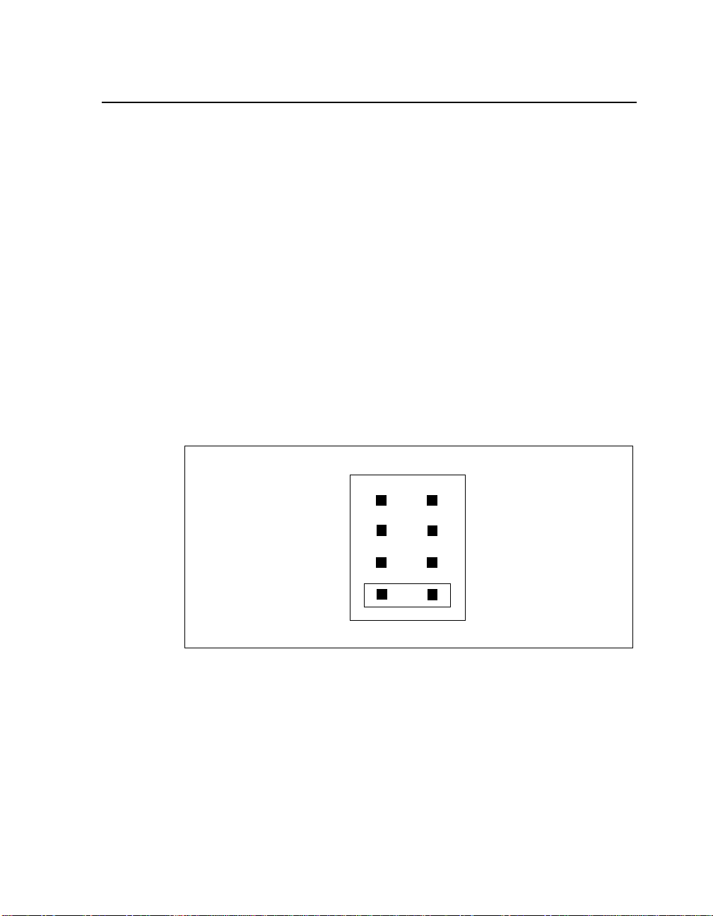
Jumper JP18
Select the boot device either from DIP memory or from PROM ICE when JP3 is
set on pin 7 and 8. The following settings indicate the possible configurations for
jumper JP18. Figure A-10 shows the jumper pins and the default setting for jumper
JP18.
• To boot from DIP memory, jumper pins 1 and 2 (shown in Figure A-10).
• To boot from PROM ICE, jumper pins 2 and 3.
DIPFCS
DIPCS
PROMCS
Figure A-10. Jumper JP18 Default Setting
1
2
3
A-12
Élan™SC520 Microcontroller Customer Development Platform User’s Manual

Jumper JP20
Use either of the following jumper settings on jumper JP20 according to your
PromICE setup.
• When using Flash memory or a modified PromICE cable, jumper pins 1 and 3
and jumper pins 2 and 4.
• When using PromICE with the original cable (requiring no cable modi fications),
jumper pins 3 and 5 and jumper pins 4 and 6.
1
3
5
Figure A-11. Jumper JP20
2
4
6
Élan™SC520 Microcontroller Customer Development Platform User’s M a nual
A-13

DIP Switch Settings
This section provides the switch settings for the three DIP switche s.
DIP Switch S3
DIP switch S3 is a single, three-circuit, slide-actuated, single-pole single-throw
(SPST) DIP switch for the system boot pinstrap. The default switch setting is shown
in Figure A-12. A description of the DIP switch settings and functions are shown
in Table A-1. For the layout location, refer to Figure 2-2 on page 2-4.
CFG0
O
N
Figure A-12. DIP Switch S3 Default Setting
Table A-1. DIP Switch S3 Settings
CFG0 CFG1 CFG2 Function
OFF OFF X BOOTCS
ON OFF X BOOTCS
OFF ON X BOOTCS
X X OFF BOOTCS
X X ON BOOTCS
CFG2
CFG1
data width = 8 bit
data width = 16 bit
data width = 32 bit
data bus = GP data bus
data bus = SDRAM data bus
A-14
Élan™SC520 Microcontroller Customer Development Platform User’s Manual

DIP Switch S4
DIP switch S4 is a slide-actuated DIP switch for the system boot pinstrap. The
default switch setting is shown in Figure A-13. The DIP switch settings (positions
2 - 8) vary according to the user-defined applications. You must define the switch
settings according to the applications being used.
For the layout location on the ÉlanSC520 microcontroller CDP, refer to
Figure 2-2 on page 2-4. Table A-2 shows the switch settings on switch S4.
1
O
N
Figure A-13. DIP Switch S4 Default Setting
Table A-2. DIP Switch S4 Settings
Switch Setting Description
1On
Off
2XDon’t care
3XDon’t care
4On
Off
5XDon’t care
6XDon’t care
23
4
Normal
Safe; resets CMOS settings on BIOS
BIOS splash displayed at startup
Memory/PCI info displayed at startup
5
6 7
8
7XDon’t care
8XDon’t care
Élan™SC520 Microcontroller Customer Development Platform User’s M a nual
A-15

DIP Switch S5
DIP switch S5 is a single three-circuit, slide-actuated DIP switch for the system
boot pinstrap. The default switch setting is shown in Figure A-14. A description
of the DIP switch settings and functions are shown in Table A-3. For the layout
location, refer to Figur e 2-2 on page 2-4.
1
O
N
Figure A-14. DIP Switch S5 Default Setting
Table A-3. DIP Switch S5 Settings
Switch 1 - DEBUG_ENTER
Setting Function
OFF Normal operation
ON AMDebug tool enabled
Switch 2 - INST_TRCE
Setting Function
OFF Normal operation
ON Trace controller enabled to output trace records
Switch 3 - DEBUG_DIS
3
2
A-16
Setting Function
OFF Normal operation
ON AMDebug tool is disabled and cannot be enabled by
software
Élan™SC520 Microcontroller Customer Development Platform User’s Manual

Appendix B
Resource Assignments
This section provides information about the resource assignm e nts for the chip
selects, GPIRQ, GPDMA, PIO, and UART.
The following information applies to the following five resource assignment tables
in this appendix:
• All PIOs are configured for alternate pin functions except PIO27, which is
default to input and works as ISA IOCHCHK.
• CBAR aliases MMC R a t DF00:0.
• Echo Mode is default to Off.
• GPCS3
• CLKTEST pin is default to output 1.8432 MHz.
• BOOTCS
-GPCS7 are chip selects, the default setting of PITGATE2, TMRIN1,
TMRIN0, TMROUT1, and TMROUT0.
, ROMCS1, and ROMCS2 are default to non-page mode (seven wait
states).
Élan™SC520 Microcontroller Customer Development Platform User’s Manual
B-1

Chip Select Resource Assignments
T ab le B-1 provides the resource assignments for the devices listed.
Table B-1. Chip Select Resource Assignments
Chip Select
BOOTCS
ROMCS1
ROMCS2
GPCS3
Settings
For JP3 and JP18, select either:
First 2M X 32 SDRAM bus bank
Second 2M X 32 SDRAM bus bank
Flash memory expansion connector
512K X 8 DIP EPROM/Flash memory
Flash memory expansion connector
For JP4, select either:
First 2M X 32 SDRAM bus bank
Second 2M X 32 SDRAM bus bank
Flash memory expansion connector
For JP5, select either:
First 2M X 32 SDRAM bus bank
Second 2M X 32 SDRAM bus bank
Flash memory expansion connector
64K X 16 SRAM on GPBUS (word access)
B-2
GPCS4
GPCS5
GPCS6
GPCS7
Élan™SC520 Microcontroller Customer Development Platform User’s Manual
Unused - for use as TMRIN1 set to input
Unused - for use as TMRIN0 set to input
IDE hard drive CS0
IDE hard drive CS1

GPIRQ Resource Assignments
T ab le B-2 provides the resource assignments for the devices listed.
Table B-2. GPIRQ Resource Assignments
ISA
SLT1
GPIRQ0 IRQ11 IRQ11 IRQ11 ——
GPIRQ1 ——IRQ1
GPIRQ2 IRQ12 IRQ12 IRQ12
GPIRQ3 IRQ3 IRQ3 IRQ3
GPIRQ4 IRQ4 IRQ4 IRQ4
GPIRQ5 IRQ5 IRQ5 IRQ5 (Lpt2)
GPIRQ6 IRQ6 IRQ6 IRQ6 (FDC) ——
GPIRQ7 IRQ7 IRQ7 IRQ7 (Lpt1) SERIRQ0 R109 —
GPIRQ8 ——IRQ8 (RTC)
GPIRQ9 IRQ9 IRQ9 IRQ9 PARIRQ R106 —
GPIRQ10 IRQ10 IRQ10 IRQ10 ENETIRQ R105 IRQ14
ISA
SLT2
Super I/O TIP IDE Hard
Drive
——
(Keyboard)
——
(Mouse)
——
1
(COM4
(COM3
(Not in use )
(Not in use )
)
——
1
)
——
SERIRQ1 R107 —
NOTE:
1. The BIOS included with CDP versi on 1.4 maps the Super I/O UAR Ts to COM3
and COM4. Earlier BIOS versions, used on boards with microcontroller revisions
A0 and A1, disabled the microcontroller’s UARTs and mapped the Super I/O
UARTs to COM1 and COM2 instead.
Élan™SC520 Microcontroller Customer Development Platform User’s Manual
B-3

GPDMA Resource Assignments
T ab le B-3 provides the resource assignments for the devices listed.
Table B-3. GPDMA Resource Assignments
ISA SLT1 ISA SLT2 Super I/O IDE Hard Drive
GPDRQ0
GPDACK0
GPDRQ1
GPDACK1
GPDRQ2
GPDACK2
GPDRQ3
GPDACK3
DRQ/DACK,
0, 1, 2, 3, 5, 6, 7,
JP6, JP7
DRQ/DACK,
0, 1, 2, 3, 5, 6, 7,
JP8, JP9
——
———
DRQ/DACK,
0, 1, 2, 3, 5, 6, 7,
JP6, JP7
DRQ/DACK,
0, 1, 2, 3, 5, 6, 7,
JP8, JP9
——
——
DRQ0/
DACK0 —
DMAREQ/
DMA_ACK
R17, R18
B-4
Élan™SC520 Microcontroller Customer Development Platform User’s Manual

PIO Resource Assignments
T ab le B-4 provides the resource assignments for the devices listed.
Table B-4. PIO Resource Assignments
PIN CDP
PIO0 GPALE P8 D14 Drives ISA ALE via buffer U20 NA NA
PIO1 GPBHE
PIO2 GPRDY P8 D15 Driven by ISA IOCHRDY, IDE hard drive
PIO3 GPAEN P8 P11 Drives ISA, Super I/O, AND tip and via
PIO4 GPTC P3 D10 Drives ISA and Super I/O TC via Buffer
PIO5 GPDRQ3 P4-16 IDE hard drive DMAREQ via R17 NA NA
PIO6 GPDRQ2 P4-11 Super I/O DRQ0 for SIO NA NA
PIO7 GPDRQ1 P4-14 ISA DRQ0, 1, 2, 3, 5, 6, 7; selected by JP8 NA NA
PIO8 GPDRQ0 P4-11 ISA DRQ0, 1, 2, 3, 5, 6, 7; selected by JP6 NA NA
PIO9 GPDACK3
PIO10 GPDACK2
PIO11 GPDACK1
PIO12 GPDACK0
PIO13 GPIRQ10 P4-12 Driven by ISA IRQ10, Super I/O IRQ10,
PIO14 GPIRQ9 P4-9 Driven by ISA IRQ9, Super I/O IRQ9, and
PIO15 GP IRQ8 P4-10 Driven by Super I/O IRQ8 and TIP
1
PROBE
P8 D12 Drives ISA BHE via bu ffer U2 0 N A NA
P4-20 IDE hard drive DMA_ACK via R18 NA NA
P4-17 Super I/ O DACK0 for SIO NA NA
P4-18 ISA DACK0, 1, 2, 3, 5, 6, 7; selected by
P4-15 ISA DACK0, 1, 2, 3, 5, 6, 7; selected by
CDP Use PIO
Input
NA NA
IOCHRDY, Super I/O IOCHRDY, and
TIP IOCHRDY. Wired OR with 1K pullup
to 5V.
NA NA
buffer U20. GP AEN used by P ALs U4 and
U6 for GP bus decode.
NA NA
U20
NA NA
JP9
NA NA
JP7
NA NA
IDE hard drive IRQ, and TI P ENETI RQ
via R015; has pullup 4K7 to 5V.
NA NA
TIP P ARIRQ via R106; has pull up 4K7 to
5V.
NA NA
SERIRQ1 via R107; has pullup 4K7 to
5V.
Output
PIO
Élan™SC520 Microcontroller Customer Development Platform User’s Manual
B-5

Table B-4. PIO Resource Assignments (Continued)
PIN CDP
PIO16 GPIRQ7 P4-7 Driven by ISA IRQ7, Super I/O IRQ7 and
PIO17 GPIRQ6 P4-8 Driven by ISA IRQ6, Super I/O IRQ6 and
PIO18 GPIRQ5 P4-5 Driven by ISA IRQ5 and Super I/O IRQ5;
PIO19 GPIRQ4 P4-6 Driven by ISA IRQ4 and Super I/O IRQ4;
PIO20 GPIRQ3 P4-3 Driven by ISA IRQ3 and Super I/O IRQ3;
PIO21 GP IRQ2 P4-4 Driven by ISA IRQ12 and Super I/O
PIO22 GP IRQ1 P4-1 Driven by Super I/O IRQ1; has pullup
PIO23 GPIRQ0 P4-2 Driven by ISA IRQ11 and Super I/O
PIO24 GPDBUFOE
PIO25 GPIOCS16
PIO26 GPMEMCS16
PIO27 PIO27 Input P4-22 Driven by ISA IOCHCK
PIO28 CTS2
PIO29 DSR2
PIO30 DC D2
PIO31 RIN2
1
PROBE
P8 D9 Enables GP data bus buffer and 512 Kbyte
P11 D15 Driven by ISA IOCS16 and IDE hard
P11 D14 Driven by ISA MEMCS16; has pullup 1K
P4-40 Drive n by CO M2 transceiver U34 (CTS) NA NA
P4-46 Driven by COM2 transceiver U34 (DSR) NA NA
P4-38 Driven by COM2 transceiver U34 (DCD) NA NA
P4-48 Drive n by CO M2 transceiver U34 (RI) NA NA
CDP Use PIO
TIP SERIRQ0 via R109; has pullup 4K7
to 5V.
TIP MAINIRQ via R108; has pullup 4K7
to 5V.
has pullup 4K7 to 5V.
has pullup 4K7 to 5V.
has pullup 4K7 to 5V.
IRQ12; has pullup 4K7 to 5V.
4K7 to 5V.
IRQ1 1; has pullup 4K7 t o 5V.
SRAM RD strobe
drive IO16
decode; has pullup 1K to 5V .
to 5V.
to 5V.
; used by PAL U4 for GP bus
; has pullup 4K7
Input
NA NA
NA NA
NA NA
NA NA
NA NA
NA NA
NA NA
NA NA
NA NA
NA NA
NA NA
Input NA
PIO
Output
B-6
Note:
1. The Probe column indicates the probe point on the CDP as the pin name (Px Dxx) or the
number (Px-xx).
Élan™SC520 Microcontroller Customer Development Platform User’s Manual

UART Resource Assignments
T ab le B-5 provides the resource assignments for the devices listed.
Table B-5. UART Resource Assignments
Device Setting
UART1 COM1 DTE on DB25M
R70 and R173, or R71 and R172 selects RS422 or RS232
1.15 Mbit/s maximum speed
UART2 COM2 DTE RS232 on DB9M
120 Kbit/s maximum speed
SSI Three devices selected by Super I/O signals:
CIO14: expansion connector JP17
CIO15: MICROWIRE EEPROM
CIO16: SPI EEPROM
Élan™SC520 Microcontroller Customer Development Platform User’s Manual
B-7

B-8
Élan™SC520 Microcontroller Customer Development Platform User’s Manual

Index
Numerics
10/100BaseT Ethernet, 2-7
A
AMDebug™ tool, 2-17
B
block diagram, 2-3
C
chip select decoder
address space, 2-16
chip select resource assignments, B-2
CodeKit software, iii
component locations, 2-4
connector
logic analyzer, 2-10, 2-12
connectors
locations, 2-5
conventions, documentation, xv
D
daughter modules, 2-18
description
ÉlanSC520 microcontroller CDP, xi
DIP switches
S3, A-14
S4, A-15
S5, A-16
display, 2-11
DMA channels
reserved for Super I/O, 2-8
DMA routing, ISA, A-6
documentation
conventions, xv
reference material, xiv
support, iii
E
ÉlanSC520 microcontroller, 2-6
ÉlanSC520 microcontroller CDP, xi
setting up, 1-2
set-up procedure, 1-5
Ethernet, 2-7
Élan™SC520 Microcontroller Customer Development Platform User’s Manual
Index-1

F
H
features, 2-1
10/100BaseT Ethernet, 2-7
AMDebug, 2-17
descripti ons, 2-6
ÉlanSC520 microcontroller, 2-6
Flash memory, 2-14
hexadecimal LED display, 2-11
high-spee d UART, 2-11
in-circuit emulator (ICE), 2-17
integrated drive electronics (IDE), 2-17
ISA card slots, 2-10
logic analyzer connector, 2-12
low-speed UART, 2-11
memory, 2-12
optional daughter modules, 2-18
PCI card slots, 2-10
SDRAM, 2-12
Super I/O, 2-8
synchronous serial interface (SSI), 2-17
test interface port (TIP) connector, 2-10
Flash memory, 2-14
configuration block diagram, 2-16
configuration diagram, 2-15
floppy disk
starting from, 1-14
G
GPDMA resource assignments, B-4
GPIRQ resource assignments, B-3
hard disk drive
starting from, 1-15
HD header J13, 2-17
HD status LED connector J13, 2-5
hexadecimal LED display, 2-11
high-spee d UART, 2-11
I
ICE, 2-17
IDE hard disk drive
starting from, 1-15
in-circuit emulator (ICE), 2-17
integrated drive electronics (IDE), 2-17
IRQs reserved for Super I/O, 2-8
ISA card slot s (GP bus slots ), 2-10
ISA-compatible signals
DMA routing, A-6
J
J12 header, 2-5
J13 header, 2-5, 2-17
JP10, A-11
JP11, A-11
JP12, A-11
JP13, A-11
JP14, A-11
JP18, A-12
JP19, 2-5
JP2, A-2
JP20, A-13
JP3, A-3
JP4, A-4
JP5, A-5
Index-2
Élan™SC520 Microcontroller Customer Development Platform User’s Manual

JP6–JP9 jumper, A-7–A-10
JTAG, 2-17
jumpers
JP10, A-11
JP11, A-11
JP12, A-11
JP13, A-11
JP14, A-11
JP18, A-12
JP2, A-2
JP20, A-13
JP3, A-3
JP4, A-4
JP5, A-5
P
PCI card slots, 2-10
pinout
jumpers JP1–JP4, A-6
PIO resource a ssignments, B-5
power LED connector J12, 2-5
PromICE
interface cable, 1-8
setting jumper JP20, 1-8
Q
L
layout, 2-4
LED, 2-11
literature support, iii
locations
components, 2-4
logic analyzer connector, 2-10
low-speed UART, 2-11
LS1, 2-5
M
memory, 2-12
chip select decoder address space, 2-16
Flash, 2-14
SDRAM, 2-12
microcontroller, 2-6
modules
daughter, 2-18
test interface port (TIP), 2-18
quick start, 1-1
R
reference material, xiv
reset switch connector JP19, 2-5
resource assignments
chip select, B-2
GPDMA, B-4
GPIRQ, B-3
PIO, B-5
UART, B-7
S
S3, A-14
S4, A-15
S5, A-16
setting up, 1-2
ÉlanSC520 microcontroller CDP, 1-2
procedure, 1-5
requirements, 1-3
speaker connector LS1, 2-5
Élan™SC520 Microcontroller Customer Development Platform User’s Manual
Index-3

starting from
floppy disk, 1-14
IDE hard disk drive, 1-15
Super I/O, 2-8
block diagram, 2-9
support, iii
synchronous serial interface (SSI), 2-17
T
technical support, iii
reference material, xiv
test interface port (TIP) connector, 2-10
third-party support, iii
U
UART
high-speed, 2-11
low-speed, 2-11
resource assignments, B-7
URL
AMD, iii
literature ordering, iii
W
www.amd.com, iii
Index-4
Élan™SC520 Microcontroller Customer Development Platform User’s Manual
 Loading...