

Page 1

AMD SB710
Databook
Technical Reference Manual
P/N: 45215_sb710_ds_pub
© 2009 Advanced Micro Devices, Inc.
Rev. 1.60
Page 2

42133
Trademarks
AMD, the AMD Arrow logo, Athlon, and combinations thereof, ATI, ATI logo, Radeon, and Crossfire are trademarks of Advanced Micro Devices, Inc.
HyperTransport is a licensed trademark of the HyperTransport Technology Consortium.
Microsoft and Windows are registered trademarks and Windows Vista is trademark of Microsoft Corporation.
Other product names used in this publication are for identification purposes only and may be trademarks of their respective companies.
Disclaimer
The contents of this document are provided in connection with Advanced Micro Devices, Inc. ("AMD") products. AMD makes no representations or warranties with
respect to the accuracy or completeness of the contents of this publication and reserves the right to make changes to specifications and product descriptions at any time
without notice. No license, w hether express, implied, arisi ng by estoppel, or otherwise, to any intellectual property rights are granted by this publication. Except as set
forth in AMD's Standard Terms and Conditions of Sale, AMD assumes no liability whatsoever, and disclaims any express or implied warranty, relating to its products
including, but not limite d to, the implied warranty of merchantability, fitness for a particular purpose, or infringement of any intellectual property right.
AMD's products are not des igned, intended, authorized or warranted for use as components in systems intended for surgical implant into the body, or in other
applications intended to support or sustain life, or in any other application in which the failure of AMD's product could create a situation where personal injury, death,
or severe property or environmental damage may occur. AMD reserves the right to discontinue or make changes to its products at any time without notice.
© 2009 Advanced Micro Devices, I nc. All rights reserved.
Page 3
Revision History
Date Revision Description
Nov, 2009 1.60 Updated Figure 3-1, “SB710 Power Up/Down Sequence”: Corrected
SLP_S5#/SLP_S3# timing diagram.
Aug, 2009 1.40 Updated Section 1.1, “Features of the SB710”: Added support for SATA hot
plug.
Updated Figure 12-1, “SB710 FCBGA Package Outline” with a picture of
better quality.
Updated Table 9-5, “RTC X1 Clock AC Specifications”: Removed cycle-to-
cycle jitter requirement.
Updated Section 7.13, “SMBus Interface/GPOC”: Noted that SCL and SDA
pins are OD when configured as SMBus pins.
July, 2009 1.25 Updated Table 9-5, “RTC X1 Clock AC Specifications”: Corrected unit for
T62 to T65 to µS.
June, 2009 1.10 First release of the public version.
Page 4

AMD SB710 Databook
45215 Rev. 1.60 November 09
Table of Contents
1 Introduction ............................................................................................................. 8
1.1 Features of the SB710.................................................................................................................... 8
1.2 Part Number and Branding........................................................................................................... 11
2 SB710 Block Diagram ........................................................................................... 12
3 SB710 Power on Sequence and Timing .............................................................. 13
3.1 Power Up and Down Sequences..................................................................................................13
4 SB710 Strap Information ...................................................................................... 18
5 Integrated Resistor and External Pull-up/Pull-down Resistor Requirements .. 22
6 SB710 Ballout Map ................................................................................................ 29
7 Signal Description................................................................................................. 31
7.1 CPU Interface ...............................................................................................................................31
7.2 LPC Interface................................................................................................................................31
7.3 A-Link Express II Interface ...........................................................................................................32
7.4 PCI Interface (PCI Host Bus and Internal PCI/PCI Bridge).......................................................... 32
7.5 USB Interface ...............................................................................................................................33
7.6 ATA66/100/133............................................................................................................................. 33
7.7 Serial ATA Interface .....................................................................................................................34
7.8 HD Audio Interface .......................................................................................................................35
7.9 Real Time Clock Interface ............................................................................................................ 35
7.10 Hardware Monitor .........................................................................................................................35
7.11 SPI ROM Interface........................................................................................................................36
7.12 Northbridge / Power Management Interface ................................................................................ 36
7.13 SMBus Interface / General Purpose Open Collector.................................................................... 38
7.14 External Event / General Event / General Power Management / General Purpose Open Collector
39
7.15 General Purpose I/O..................................................................................................................... 41
7.16 Integrated Micro-Controller (IMC).................................................................................................45
7.17 Reset / Clocks / ATE.....................................................................................................................46
7.18 Intruder Alert .................................................................................................................................47
7.19 Power and Ground........................................................................................................................ 47
8 Functional Description ......................................................................................... 49
8.1 EHCI USB 2.0 and OHCI USB 1.1 Controllers............................................................................. 49
8.1.1 USB Power Management.....................................................................................................................50
8.2 SMI#/SCI Generation ...................................................................................................................51
8.3 LPC ISA Bridge.............................................................................................................................52
8.3.1 LPC Interface Overview .......................................................................................................................52
8.3.2 LPC Module Block Diagram .................................................................................................................54
8.4 Integrated Micro-Controller (IMC).................................................................................................54
8.4.1 Consumer Infrared Controller...............................................................................................................54
8.5 Real Time Clock ...........................................................................................................................55
4 Table of Contents
Page 5

45215 Rev. 1.60 November 09
8.5.1 Functional Blocks of RTC.....................................................................................................................55
8.6 PATA Controller............................................................................................................................ 56
8.7 SATA (Serial ATA) Controller ....................................................................................................... 57
8.8 PCI Bridge ....................................................................................................................................58
8.9 High Definition Audio ....................................................................................................................58
8.9.1 HD Audio Codec Connections..............................................................................................................58
8.10 Power management/ACPI ............................................................................................................ 58
8.11 General Events and GPIOs ..........................................................................................................59
8.12 Hardware Monitor Interface ..........................................................................................................59
AMD SB710 Databook
9 System Clock Specifications................................................................................ 61
9.1 System Clock Descriptions and Frequency Specifications .......................................................... 61
9.2 System Clock AC Specifications ..................................................................................................62
10 States of Power Rails during ACPI S1 to S5 States ........................................... 65
11 Electrical Characteristics ..................................................................................... 66
11.1 Absolute Maximum Ratings.......................................................................................................... 66
11.2 Functional Operating Range for Signal Input ...............................................................................66
11.3 DC Characteristics........................................................................................................................67
11.4 Reset Signal Requirements ..........................................................................................................72
11.5 RTC Battery Current Consumption...............................................................................................72
12 Package Information ............................................................................................. 73
12.1 Physical Dimensions.....................................................................................................................73
12.2 Pressure Specification.................................................................................................................. 74
13 Thermal Information.............................................................................................. 74
14 Testability .............................................................................................................. 75
14.1 Test Control Signals ..................................................................................................................... 75
14.2 XOR Chain Test Mode .................................................................................................................76
14.2.1 Brief Description of an XOR Chain.......................................................................................................76
14.2.2 Description of the SB710 XOR Chain...................................................................................................77
Appendix A: Pin Listing.............................................................................................. 82
Table of Contents 5
Page 6

AMD SB710 Databook
45215 Rev. 1.60 November 09
List of Figures
Figure 1-1: SB710 Branding Diagram ..........................................................................................................................11
Figure 2-1: SB710 Block Diagram Showing the Internal PCI Devices and Major Function Blocks ..............................12
Figure 3-1: SB710 Power Up/Down Sequence ............................................................................................................14
Figure 3-2: SB710 S3/S0 Power Up/Down Sequence .................................................................................................15
Figure 3-3: Circuit for Maintaining Proper Relationship between +V5_VREF and VDDQ ............................................16
Figure 3-4: Timing for SB PWR_GOOD De-asserted to RSMRST# De-asserted........................................................17
Figure 3-5: Timing for LDT_STP# assertion on first power up (G3 S5) ...................................................................17
Figure 3-6: S5_3.3V Power Down Sequence Requirement .........................................................................................17
Figure 4-1: Straps Capture...........................................................................................................................................18
Figure 4-2: Type II Straps Capture timing ....................................................................................................................18
Figure 4-3: Type I Straps Capture timing .....................................................................................................................19
Figure 6-1: SB710 Ball-out Assignment (Left) ..............................................................................................................29
Figure 6-2: SB710 Ball-out Assignment (Right) ...........................................................................................................30
Figure 8-1: SB710 USB 2.0 System Block Diagram.....................................................................................................49
Figure 8-2: A Typical LPC Bus System........................................................................................................................52
Figure 8-3: LPC control signals diagram (TBA)............................................................................................................52
Figure 8-4: Block Diagram of LPC Module...................................................................................................................54
Figure 8-5: Block Diagram of the integrated micro-controller Module (TBA) ................................................................54
Figure 8-6: Block Diagram of Internal RTC ..................................................................................................................56
Figure 8-7: Block Diagram for the SATA Module .........................................................................................................57
Figure 8-8: HD Audio Codec Connections ...................................................................................................................58
Figure 9-1: Timing Labels for AC Specifications of the SB710 Clocks .........................................................................62
Figure 9-2: Timing Labels for AC Specifications of the SB710 Diff Clocks...................................................................62
Figure 9-3: SB710 Diff Clocks Rise and Fall Time Measurement ................................................................................62
Figure 12-1: SB710 21 mm x 21 mm 0.8 mm Pitch 528-FCBGA Package Outline ......................................................73
Figure 14-1: Test Mode Capturing Sequence Timing...................................................................................................76
Figure 14-2: A Generic XOR Chain..............................................................................................................................76
Figure 14-3: On-chip XOR Chain connectivity .............................................................................................................77
6 List of Figures
Page 7

45215 Rev. 1.60 November 09
AMD SB710 Databook
List of Tables
Table 1-1: SB710 Part Numbers ..................................................................................................................................11
Table 3-1: SB710 Power Up/Down Sequence Timing..................................................................................................13
Table 4-1: Standard Straps ..........................................................................................................................................19
Table 4-2: Debug Straps ..............................................................................................................................................20
Table 4-3: Additional Straps .........................................................................................................................................21
Table 5-1: External Resistor Requirements and Integrated Pull-Up/Down...................................................................22
Table 8-1: EHCI Support for Power Management States.............................................................................................50
Table 8-2: EHCI Power State Summary.......................................................................................................................50
Table 8-3: Causes of SMI# and SCI.............................................................................................................................51
Table 8-4: LPC Cycle List and Data Direction..............................................................................................................53
Table 8-5: SMI, SCI, and Wake Event Support by GPIO and General Event Pins ......................................................59
Table 8-6: Functionality of the General Events and GPIOs across ACPI States..........................................................59
Table 9-1: SB710 System Clock Descriptions..............................................................................................................61
Table 9-2: SB710 System Clock Input Frequency Specifications ................................................................................61
Table 9-3: SB710 System Clock Output Frequency Specifications..............................................................................61
Table 9-4: 48MHz USB/SIO Clock AC Specifications ..................................................................................................63
Table 9-5: RTC X1 Clock AC Specifications ................................................................................................................63
Table 9-6: LPC Clock AC Specifications ......................................................................................................................63
Table 9-7: PCI Clock AC Specifications .......................................................................................................................64
Table 9-8: PCI-E Clock AC Specifications ...................................................................................................................64
Table 9-9: RTC 32-KHz Output Clock AC Specifications .............................................................................................64
Table 10-1: State of Each Power Rail during ACPI S1 to S5 States ............................................................................65
Table 11-1: Absolute Maximum Rating ........................................................................................................................66
Table 11-2: DC Characteristics for Power Supplies to the SB710 ...............................................................................67
Table 11-3: DC Characteristics for Interfaces on the SB710........................................................................................67
Table 11-4: GPIO/GEVENT Input DC Characteristics..................................................................................................68
Table 11-5: GPIO/GEVENT Output DC Characteristics...............................................................................................71
Table 11-6: RTC Clock Output DC Characteristics ......................................................................................................71
Table 11-7: Reset Signal Requirements ......................................................................................................................72
Table 11-8: RTC Battery Current Consumption ...........................................................................................................72
Table 12-1: SB710 21 mm x 21 mm 0.8 mm Pitch 528-FCBGA Physical Dimensions ................................................73
Table 13-1 SB710 Thermal Limits................................................................................................................................74
Table 14-1: Signals for the Test Controller of the SB710 .............................................................................................75
Table 14-2: Test Mode Signals ....................................................................................................................................75
Table 14-3: TEST0 Bit Sequence.................................................................................................................................75
Table 14-4: Truth Table for an XOR Chain ..................................................................................................................77
Table 14-5: List of Pins on the SB710 XOR Chain and the Order of Connection.........................................................77
Table 14-6: Pins Excluded from the XOR Chain ..........................................................................................................81
List of Tables 7
Page 8

AMD SB710 Databook
45215 Rev. 1.60 Nov 09
1 Introduction
AMD’s SB710 is a Southbridge that integrates key I/O, communication, and audio features required in a
state-of-the-art PC into a single device. Over and beyond the features supported by the SB700, the
SB710 also supports a number of hardware monitoring features and AMD’s Advanced Clock Calibration
utility. It is specifically designed to operate with AMD’s integrated graphics processors (IGPs) and
Northbridges in desktop and mobile PCs.
1.1 Features of the SB710
CPU Interface
Supports AMD Athlon™ 64 and Athlon 64
FX , Opteron™, Dual-Core Opteron™
Sempron™, Mobile Sempron™, Athlon XPM, and Turion™ processors. Dual-core
CPUs are supported.
A-Link Express II interface to AMD
Northbridges
1 / 2 / 4-lane A-Link Express II interface
Dynamic detection of lane configuration
High data transfer bandwidth (up to 2.5 Gb/s
/ Lane)
PCI Host Bus Controller
Supports PCI bus at 33 MHz
PCI Rev. 2.3 specification support
Supports up to 6 bus master devices
SMBus Controller
SMBus Rev. 2.0 compliant
Support SMBALERT # signal / GPIO
Interrupt Controller
Supports IOAPIC/X-IO APIC mode for 24
channels of interrupts
Supports 8259 legacy mode for 15 interrupts
Supports programmable level/edge
triggering on each channels
Supports serial interrupt on quiet and
continuous modes
DMA Controller
Two cascaded 8237 DMA controllers
Supports PC/PCI DMA
Supports 40-bit addressing
Interrupt steering supported for plug-n-play
devices
BIOS / Hardware support to hide PCI device
Spread spectrum support
USB Controllers
5 OHCI and 2 EHCI Host controllers to
supports 12 USB 2.0 ports and 2 dedicated
USB 1.1 ports
ACPI S1 ~ S5 supported
Legacy Keyboard/Mouse support
USB debug port
Port disable supported with individual control
Supports LPC DMA
Supports type F DMA
LPC Host Bus Controller
Supports LPC based super I/O and flash
Two Master/DMA devices supported
Support for TPM version 1.1/1.2 devices
Supports SPI devices
SATA Controller
Supports six SATA ports with transfer rates
Complies with SATA 2.5 specification
8 Introduction
devices
up to 3 Gb/s
Page 9

45215 Rev. 1.60 November 09
Supports both SATA 1.5 and SATA 3.0
compliance devices
Two modes of operation are supported
Legacy Mode using I/O space
AHCI mode using the Memory space
Parallel ATA emulation supported to allow
seamless support for IDE software.
Supports e-SATA
Supports hot plug for AHCI mode
Legacy IDE Emulation Support
Legacy Mode using I/O space
Parallel ATA emulation supported to allow
seamless support for IDE software.
AMD RAID Support
Supports integrated RAID 0, RAID 1, and
RAID 10 (requires use of 4 or more SATA
ports) functionalities across all 6 ports.
AHCI Support
AHCI mode using the memory space
AMD SB710 Databook
4 Independent input streams (DMA)
Multiple channels of audio output per stream
Support up to 4 codec’s
Up to 192 kHz Sample Rate and 32-bit
Audio
64-bit addressing capability for DMA Bus
Master
Unified Audio Architecture (UAA) compatible
HD Audio registers can be located anywhere
in the 64-bit address space
Timers
8254 compatible timer
Microsoft High Precision Event Timer
(HPET)
ACPI power management timer
Watchdog timer
RTC (Real Time Clock)
256-byte battery-backed CMOS RAM
Hardware supported century rollover
RTC battery monitoring feature
Supports AHCI hardware assist to support
advanced features such as NCQ (Native
Command Queuing), Hot Plug, and Device
or Host initiated power Management (DIPM
/HIPM)
IDE Controller
Single PATA channel support
Supports PIO, Multi-word DMA, and Ultra
DMA 33/66/100/133 modes.
32x32-byte buffers each channel for
buffering
Swap bay support by tri-state IDE signals
Supports Message Signaled Interrupt
(MSI).
Integrated IDE series resistor
High Definition Audio
4 Independent output streams (DMA)
Power Management
ACPI specification 3.0 compliant power
management schemes
Supports C1e, C2, C3 and C3 pop-up
Supports S0, S1, S3, S4, and S5
Wakeup events for S1, S3, S4/S5 generated
by:
Any GEVENT pin
Any GPM pin
USB
Power Button
Internal RTC wakeup
SMI# event
Full support for On-Now
CPU SMM support, generating SMI# signal
upon power management events
GPIO supports on external wake up events
Introduction 9
Page 10

AMD SB710 Databook
CLKRUN# supported on PCI power
management
ALPM (HIPM) on SATA
DIPM on SATA
Note: Advanced Power Management (APM) is
not supported.
Hardware Monitor
Hardware monitoring support for voltage
sensors, fan control, and digital TSI to AM3
processors. Note: Temperature monitoring
is NOT supported.
Integrated Micro-Controller (IMC)*
Supports integrated IR transceivers for
Media Center applications.
45215 Rev. 1.60 November 09
* Note: While the IMC block on the SB710 has
to be enabled for infrared controller interface
support, no IMC advanced features (like
keyboard scan matrix, PS2, or power
management controllers) are supported by the
SB710 even if the term "IMC" may appear in
block name, pin names, register names, or
register field names, etc., of the device.
Over Clocking
Provides support for enhanced CPU
performance tuning using the AMD
Advanced Clock Calibration (ACC)
performance tuning utility.
10 Introduction
Page 11
45215 Rev. 1.60 November 09
1.2 Part Number and Branding
AMD SB710 Databook
Figure 1-1: SB710 Branding Diagram
Note 1: Marketing logo
Note 2: AMD product type
Note 3: Date Code (YYWW). YY-assembly start year, WW-assembly start week.
Note 4: COO. Country of origin (assembly site)
Note 5: This is wafer foundry’s lot number for the product.
Note 6: AMD part number (see Table 1-1 below)
Table 1-1: S
Substrate
Revision
C A14 218-0660017
710 Part Numbers
B
ASIC
Revision
AMD Part Number
Introduction 11
Page 12
AMD SB710 Databook
2 SB710 Block Diagram
45215 Rev. 1.60 November 09
Figure 2-1: SB710 Block Diagram Showing the Internal PCI Devices and Major Function Blocks
12 SB710 Block Diagram
Page 13
45215 Rev. 1.60 November 09
AMD SB710 Databook
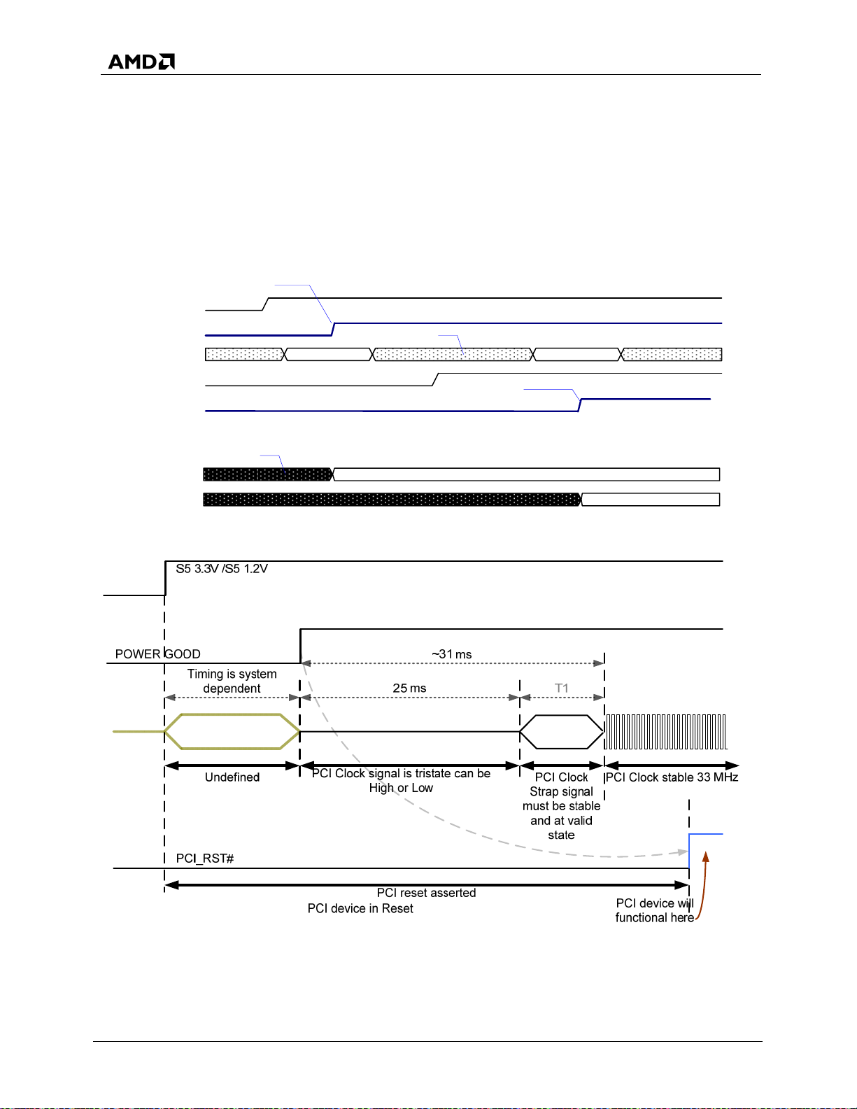
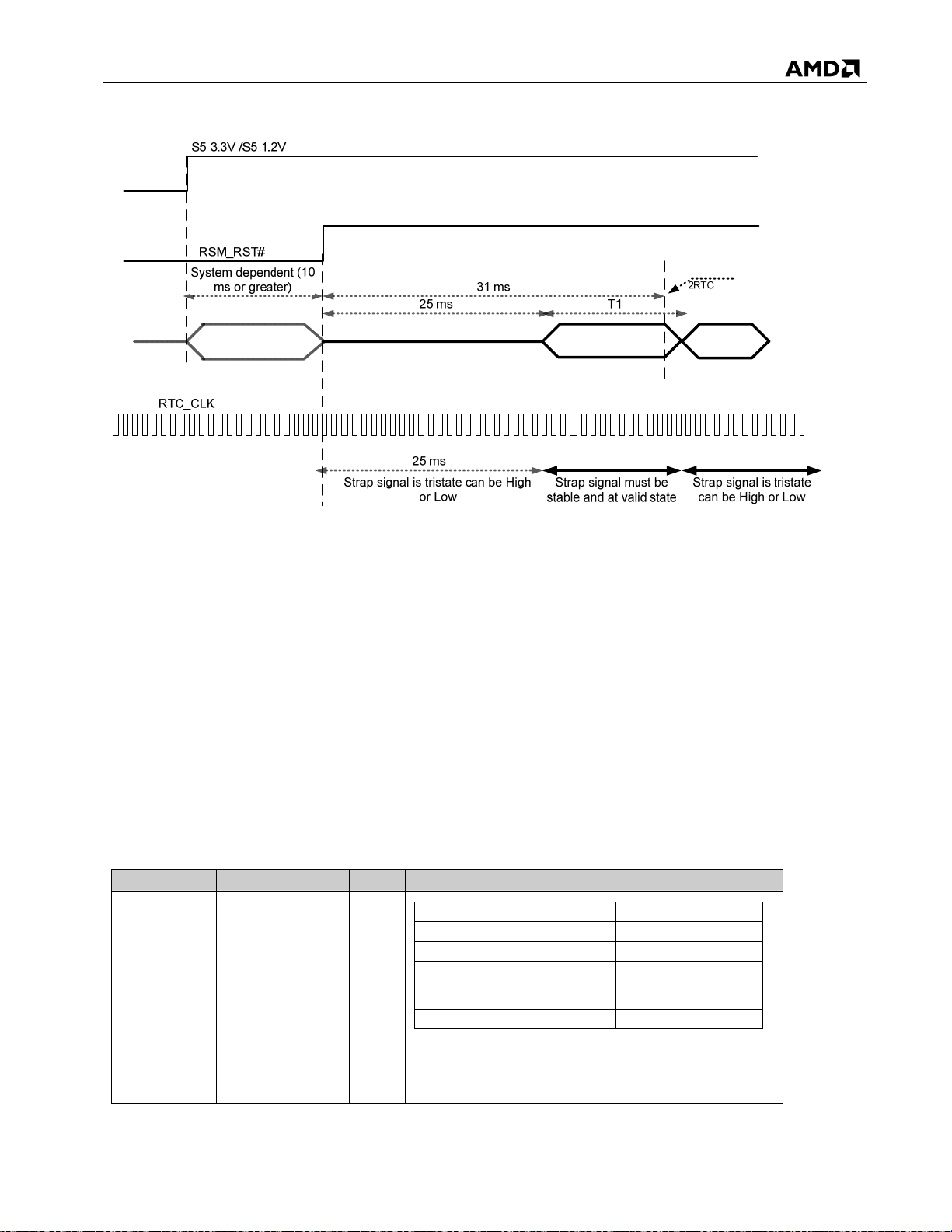
3 SB710 Power on Sequence and Timing
3.1 Power Up and Down Sequences
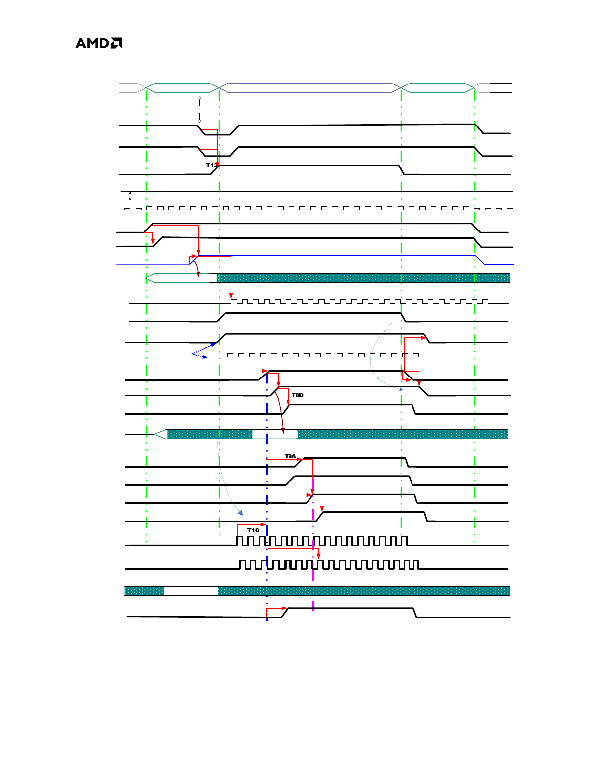
Simple diagrams of the SB710 power up sequences are shown in Fi gure 3-1 and Figure 3-2 below. A
power detection circuit is integrated into the SB710. This circuit will monitor SB PWR_GOOD and will
assert A_RST# and LDT_RST# for as long as SB PWR_GOOD is false. After SB PWR_GOOD has been
asserted, A_RST#, followed by LDT_RST#, will be de-asserted. Table 4-1 shows the timing requirements
referenced in Figure 3-1 th
rough Figure 3-5
the ramp time for any rail be less than 40ms.
Table 3-1: SB710 Power Up/Down Sequence Timing
Symbol Min. Max. Description
T1
T2 10 ms – +3.3V_S5 to resume reset (RSMRST#).
T2A – 50 ms
T3 32 ms – RSMRST# de-asserted to Start of RTCCLK output from SB710.
T4 50 ns SB PWR_GOOD de-assertion to NB_PWRGD de-assertion delay.
T7 0 ns 30 ns
T7A – 50 ms
T7B – 1 ms SB PWR_GOOD fall time.
T8A
T8B –
T8C 1.0 ms 2.3 ms PCIRST# to LDT_RST#.
T8D 98 ms 108 ms NB_PWRGD to LDT_PG.
T9 101 ms 113 ms SB PWR_GOOD to PCIRST#.
T9A 101 ms 113 ms SB PWR_GOOD to A_RST# (T9-T8A).
T9B 31 ms –
T10 -31 ms – PCIE_CLKP/N stable time before SB PWRGOOD assertion.
T11 36 ms 41 ms
T13
T13A 80 ns –
T14 1 ns –
T15 5 s –
T16A 40 µs – LDT_STP# assertion to LDT_RST# assertion.
T16B 4 µs – LDT_RST# assertion to SLP_S3# assertion.
Note 1
0 ns
Note 4
– 15 ns Wake Event (except PwrButton) to SLP_S3# / SLP_S5#.
200 ns – Wake Event (PwrButton) to SLP_S3# / SLP_S5# (S5/S4/S3 S0)
8 ns -- Wake Event (PwrButton) to SLP_S3# / SLP_S5# (G3 S5 S0)
100 ns A_RST# (PCI host bus reset) to PCIRST#.
Note 5
+3.3V_S5 to +1.2V_S5
Resume reset (RSMRST#) rise time (10% to 90%). SB710 has a Schmitt trigger
input with de-bouncing logic on this pin, so the value is relaxed relative to earlier
AMD SB designs.
SB PWR_GOOD assertion to NB_PWRGD assertion delay when using the
SB710 NB_PWRGD output. This parameter is the internal delay of the SB. The
system board design may add additional delay due to loading and trace length.
The acceptable delay including system layout / loading is 1 ms maximum..
SB PWR_GOOD rise time (10% to 90 %). See Note 3. SB710 has a Schmitt
trigger with de-bouncing logic on this pin, so the value is relaxed relative to
earlier AMD SB designs.
KBRST# to A_RST#.
SB PWR_GOOD to LDT_STP#. See Note 11
SB PWR_GOOD to stable PCICLK 33 MHz. See Note 8.
SB PWR_GOOD must be de-asserted before VDD (PS PWOK) drops more than
5% off the nominal value. See Note 9.
SB PWR_GOOD de-assertion to Resume Reset (RSMRST#) assertion. See
Note 10.
[Not illustrated] VBAT to +3.3V_S5 to +1.2V_S5. Must be greater than 5
seconds to allow start time for the internal RTC.
. Besides the illustrated requirements, it is also required that
See Notes 1 to 12 in the Power Up Sequence Timing Notes section following the timing diagrams.
SB710 Power on Sequence and Timing 13
Page 14
AMD SB710 Databook
S5
PWR_BTN#
WAKE#
SLP_S5#/
SLP_S3#
VBAT
RTC clock In
VBAT
Wake Event
45215 Rev. 1.60 November 09
S0
S5 G3G3
+3.3V_S5
1.2V_ S5
RSMRST#
RTCCLK out
PS PWOK
S 0 power rails
System clocks
SB PWR_ GOOD
NB_ PWRGD
LDT_PG
A_ RST#
KBRST#
PCIRST#
( See Note 1)
( See Note 1 & 2)
T1
T2A
S 5 STRAPS
T2
T3
T13A
T7A
T7
S 0 STRAPS
( See Note 6)
T8B
( See Note 5)
T8A
T9
( See Note 4)
T8C
T4
T7B
LDT_ RST#
PCIE_ RCLKP/N
PCICLK[5:0]
ALLOW_ LDTSTP
LDT_STP#
( Note 8)
Note 11
T11
T9B
Figure 3-1: SB710 Power Up/Down Sequence
14 SB710 Power on Sequence and Timing
Page 15
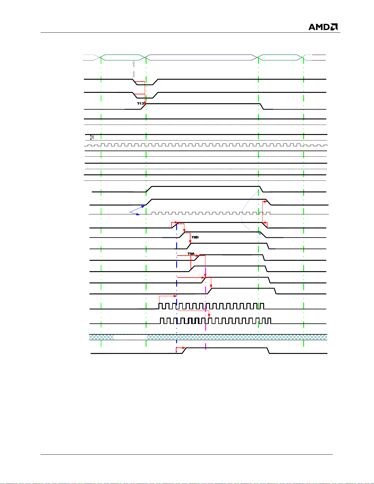
45215 Rev. 1.60 November 09
PWR_BTN#
WAKE#
SLP_S3#
S3
Wake Event
S0
AMD SB710 Databook
S3
SLP_S5#
VBAT
RTC clock
+3.3V_S5
+1.2V_S5
RSMRST#
PS PWOK
S0 power rails
System clocks
SB PWRGOOD
NB_PWRGD
LDT_PG
A_RST#
KBRST#
PCIRST#
LDT_RST#
GND
GND
GND
GND
GND
(See Note 1 & 2)
T7A
T10
T13A
T7
T8B
(See Note 5)
T8A
(See Note 4)
T9
T8C
T7B
PCIE_RCLKP/N
ALLOW_LDTSTP
PCICLK[5:0]
LDT_STP#
T11
(Note 8)
T9B
Figure 3-2: SB710 S3/S0 Power Up/Down Sequence
SB710 Power on Sequence and Timing 15
Page 16
AMD SB710 Databook
45215 Rev. 1.60 November 09
Power up Sequence Timing Notes
Note 1: There is no specific power sequencing requirement other than those indicated in Note
2 below. The SB710 power rails are grouped in four different voltages:
I. +5 V, which includes V5_VREF
II. +3.3 V, which includes VDDQ, VDD33_18 (IDE mode)
III. +1.2 V, which includes AVDDCK_1.2V, AVDD_SATA, PLLVDD_SATA, PCIE_PVDD,
PCIE_VDDR, CKVDD_1.2V
IV. +1.8 V
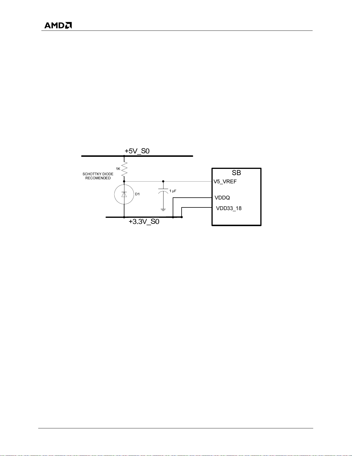
Note 2: V5_VREF is used in the SB710 for the 5-V PCI signal tolerance. VDDQ (+3.3 V) &
VDD33_18 (3.3 V) must not exceed V5_VREF by more than 0.6 V at any time during ramp up,
steady state, or ramp down. The suggested circuit below should be used to maintain
relationship between V5_VREF and VDDQ and VDD33_18.
Figure 3-3: Circuit for Maintaining Proper Relationship between +V5_VREF and VDDQ
Note 3: The SB710 will latch the straps after rising edge of SB PWR_GOOD only once. With
debouncing of SB PWR_GOOD, the latching of strap will occur at approximately ~10ms after
the rising edge of SB PWR_GOOD.
Note 4: Typical time between A_RST# and PCIRST# is 75 ns. The measurement should be
done at 10% of both signals. Loading on the motherboard may cause the measurement at
90% be more than the spec.
Note 5: The KBRST# should be de-asserted before A_RST# (LDT_RST#) is de-asserted.
Note 6: Type II Standard and Debug straps will be latched after SB PWR_GOOD is asserted.
Type I straps are latched on resume reset rising edge. Refer to Section 4: SB710 Strap
Information for stra
Note 7: The SB710 will not monitor the ALLOW_LDTSTP signal on power up. This signal is
only used on C3 transitions.
Note 8: The PCI Clock may be stable before T11 min. under some conditions; however in all
cases, the PCI Clock is guaranteed to be stable only between T11 min and max.
Note 9: The SB710 will monitor internally the power down events and protect the internal
circuit during the power down event. This includes power down during the S3, S4, and S5
states. During an unexpected power failure or G3 state, the relationship between the 1.2 V
(VDD) and SB Power Good should be maintained to protect the internal logic of the SB710.
p timing.
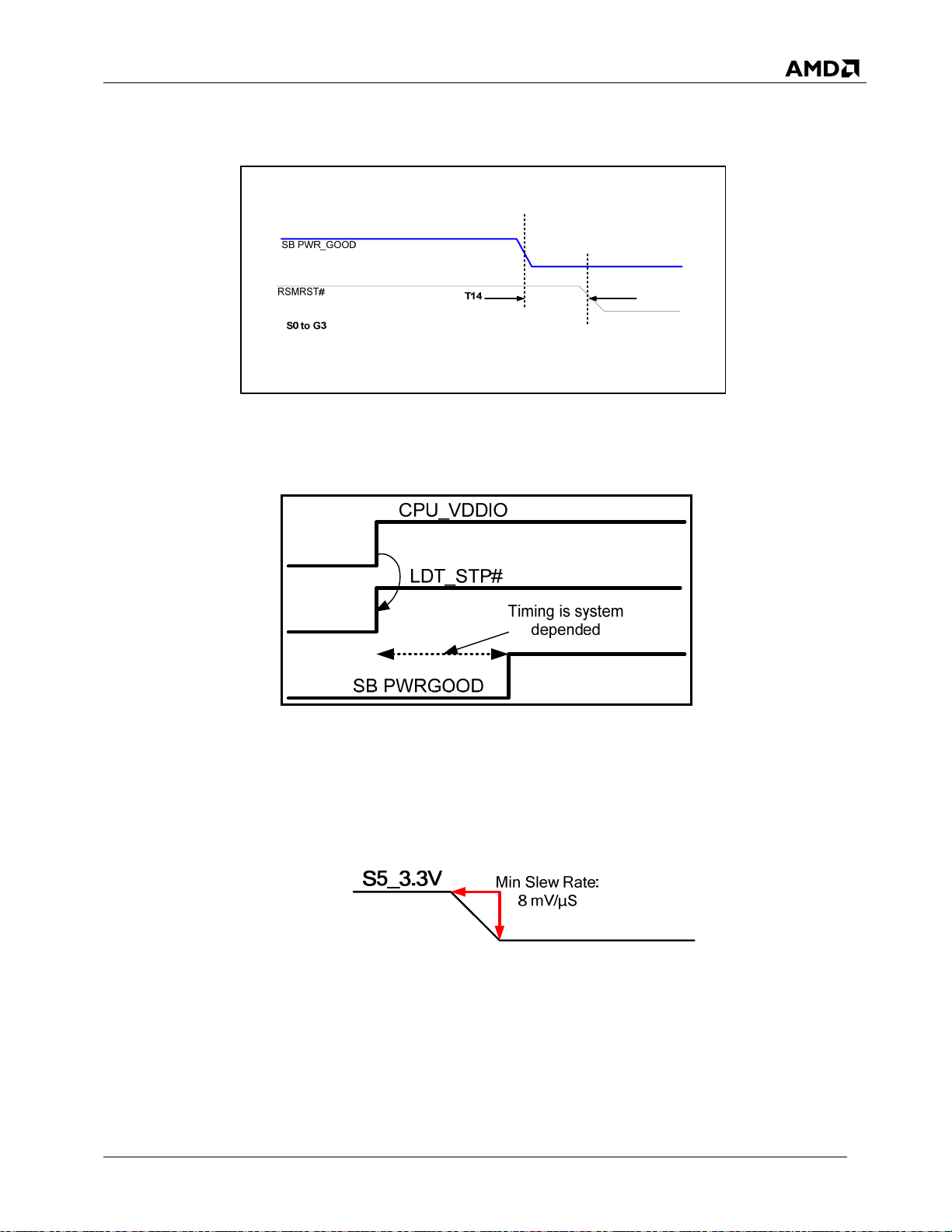
Note 10: The following figure shows the timing of SB PWR_GOOD de-asserted to RSMRST#
de-asserted during a power down sequence. However, this timing only applies to S0 to G3
state transition, because G3 state is where both signals are inactivated.
16 SB710 Power on Sequence and Timing
Page 17
45215 Rev. 1.60 November 09
AMD SB710 Databook
Figure 3-4: Timing for SB PWR_GOOD De-asserted to RSMRST# De-asserted
Note 11: On first power up, G3 S5, or after RSMRST# assertion, the LDT_STP# will be asserted
with CPU_VDDIO power. On subsequent power up, S5 S0, the timing on T9B will apply.
Figure 3-5: Timing for LDT_STP# assertion on first power up (G3 S5)
Note 12: The S5_3.3V ramp down should be controlled to achieve a slew rate of 8mV/ µS or lower.
Figure 3-6: S5_3.3V Power Down Sequence Requirement
SB710 Power on Sequence and Timing 17
Page 18
AMD SB710 Databook
45215 Rev. 1.60 November 09
4 SB710 Strap Information
There are two kinds of strap-latching logic, Type I and Type II. Type I straps will be latched on G3 to S5
transition on rising edge of RSMRST#. Type II straps are latched on S5 to S0 transition after rising edge
of PWR_GOOD assertion.
Straps I
Capture
S5_1.2V
RsmRst#
STRAPs (board)
VDD
PwrGood
Straps Type I
Straps Type II
Undefined
Don' t care
Straps I
Figure 4-1: Straps Capture
Straps II
Capture
Straps Type I
Straps II
Straps Type II
Figure 4-2: Type II Straps Capture timing
18 SB710 Strap Information
Page 19
45215 Rev. 1.60 November 09
AMD SB710 Databook
Figure 4-3: Type I Straps Capture timing
Straps are also classified in two groups, standard and debug. Straps in the standard group are used for
selecting on power up the desired modes of ASIC operation and additional optional features. Straps in
debug group are for debugging at the system-level, mainly during the pre-production stage. Debug straps
should have provision for PU or PD so they can be configured to either option when required for debug
purposes.
Table 4-1 an
d Table 4
-2 show the function of every strap signal in the design. All straps are defined such
that in the most likely scenario of operation, they will be set to the recommended (or safest) values. The
values shown in the Description column are the external board strap values, with 3.3V being a pull-up
(PU) and 0V a pull-down (PD).
Table 4-1: Standard Straps
Pad Name Strap Name Type Description
ROM_TYPE_1 ROM_TYPE_0 ROM Type
3.3 V 3.3 V Reserved
3.3 V 0 V SPI ROM
{IMCGPIO17,
IMCGPIO16 }
{ ROM_TYPE_1,
ROM_TYPE_0 }
0 V 3.3 V LPC ROM (Supports
I
0 V 0 V Firmware Hub
both LPC and PMC
ROM types)
These two strap pins should be configured to the
corresponding state that matches the Hardware
ROM type installed.
SB710 Strap Information 19
Page 20
AMD SB710 Databook
Pad Name Strap Name Type Description
IMC_ENABLE
Integrated Microcontroller (IMC)
I
0 V – Disable IMC
3.3 V – Enable IMC. Required for IR controller support.
45215 Rev. 1.60 November 09
LPCCLK0
PCI_ROM_BOOT
LPCCLK1
AZ_RST#
PCICLK5 Reserved — Reserved
PCICLK4 Reserved — Reserved
PCIE_PLL_ENAB
LE
IMC_ENABLE
PCI_ROM_BOOT
Revision A11 strap defination
Booting from PCI memory
0 V – disable PCI ROM boot (Default)
II
II
I
II
3.3 V – enable PCI ROM boot
Note: This feature is for debug pupose only. After a G3
S5 transition the system will allow boot from PCI memory
only once. Subsequent S5 S0 transition will not boot
from PCI memory.
Enable PCI-E PLL
0 V – Normal operation. PCI-E clock enabled for
internal PLL reference clock.
3.3 V – Test / debug. PCI-E clock disconnected from
internal PLL.
Revision A11 strap defination
Integrated Microcontroller (IMC)
0 V – disable IMC
3.3 V – enable IMC
Booting from PCI memory
0 V – disable PCI ROM boot (Default)
3.3 V – enable PCI ROM boot
Note: This feature is for debug pupose only. After a G3
S5 transition the system will allow boot from PCI memory
only once. Subsequent S5 S0 transition will not boot
from PCI memory.
Enable/Disable additional straps for debugging (see
Table 4-2)
PCICLK3
PCICLK2 Watchdog_Enable
Debug_Straps
II
II
0 V – use hardcoded defaults for Debug
Straps (Default)
3.3 V – enable additional Debug Straps
Watchdog function
0 V – disable watchdog function on NB_PWRGD ball
3.3 V – enable watchdog function on NB_PWRGD ball
Table 4-2: Debug Straps
Pad Name Strap Name Type Description
PCI_AD30 Reserved —
PCI_AD29 Reserved —
PCI_AD28 Reset_Length
Reserved (Internal PU of 15 k)
Reserved (Internal PU of 15 k)
Generate a short reset
II
0 V – Use short reset (reserved, do not use)
3.3 V – Use long reset (Default)
(Internal PU of 15 k)
20 SB710 Strap Information
Page 21

45215 Rev. 1.60 November 09
Pad Name Strap Name Type Description
Bypass PCI PLL
0 V – Bypass internal PLL clock .
Use REQ3# as A-Link bypass clock
PCI_AD27 PCI_PLL
PCI_AD26 ACPI_BCLK
PCI_AD25 IDE_PLL
PCI_AD24 PCIE_EEPROM
PCI_AD23 Reserved —
II
II
II
II
Use GNT3# as B-Link bypass clock
3.3 V – Use internal PLL-generated PLL
CLK (Default)
(Internal PU of 15 k)
Bypass ACPI_BCLK
0 V – Bypass internal generated acpi_bclk.
GNT0# as acpi_bclk bypass clock.
3.3 V – Use internal generated acpi_bclk (Default)
(Internal PU of 15 k)
Bypass IDE CLK
0 V – Bypass internal Ide Clk
Use GNT2# as Ide 66-MHz bypass clock.
Use REQ2# as Ide 50-MHz bypass clock.
Use REQ1# as Ide 33-MHz bypass clock.
3.3 V – Use internal PLL Ide Clk (Default)
(Internal PU of 15 k).
A-Link Express-II core strap from I2C ROM enable
0 V – Use EEPROM PCI-E straps, getting the value
from I2C EPROM.
I2C EPROM ADDRESS set to all zeroes.
Use GNT4# as SDA
Use REQ4# as SCL.
3.3 V – Use default PCI-E straps (Default)
(Internal PU of 15 k)
Reserved (Internal PU of 15 k)
AMD SB710 Databook
Table 4-3: Additional Straps
The following strap is not captured by the straps logic, but is required to make the internal RTC work
properly.
Pad Name Strap Name Description
The pin should be pulled-up to S5_3.3V and a crystal should be put
RTCCLK —
on X1/X2 to enable the internal RTC. Otherwise, the internal RTC
may not function properly
SB710 Strap Information 21
Page 22
AMD SB710 Databook
45215 Rev. 1.60 November 09
5 Integrated Resistor and External Pull-up/Pull-down
Resistor Requirements
Table 5-1: External Resistor Requirements and Integrated Pull-Up/Down
Interface Signal Name
IDE
IDE_DRQ Integrated 5.6 K Pull-down —
IDE_IORDY Integrated 4.7 K Pull-up —
IDE_IRQ Integrated 10 K Pull-down —
IDE_D7/GPIO22
IDE_D[15:0]/GPIO[30:23, 21:15]
IDE_A[2:0]
IDE_CS[3,1]#
IDE_DACK#, IOW#, IOR#,
PCIE_CALRP
PCIE_CALRN External 2.05 K ( 1%
Value of
Integrated / External
Resistor
Integrated 27 +
integrated 10 K
Integrated 27
Integrated 27
Integrated 27
Integrated 27
External 562 ( 1%
tolerance )
Reference resistor for
the Tx termination.
tolerance )
Reference resistor for
the Rx termination
Resistor Type
Series + Pulldown
Series
Series —
Series —
Series ——
Pull-down to
VSS_PCIE
Pull-UP to
VDD_PCIE
Register for
programming the
integrated PU/PD
(See GPIO section
below)
PCI-E
—
USB
HD Audio
NB ALLOW_LDTSTP External Pull-up Pull-up —
Processor
PCI
USB HSD[11:0]P Integrated 15 K Pull-down —
USB_HSD[11:0]N Integrated 15 K Pull-down —
USB_FSD[13:12]P Integrated 15 K Pull-down —
USB_FSD[13:12]N Integrated 15 K Pull-down —
AZ_SDIN[2:0]/
GPIO[44:42]
AZ_SDIN3/GPIO46 Integrated 50 K Pull-down (See GPIO section
LDT_PG External Pull-up Pull-up —
LDT_STP# External Pull-up Pull-up —
LDT_RST# External Pull-up Pull-up —
INTE#/GPIO33 Integrated 8.2 K Pull-up (See GPIO section
INTF#/GPIO34 Integrated 8.2 K Pull-up (See GPIO section
INTG#/GPIO35 Integrated 8.2 K Pull-up (See GPIO section
INTH#/GPIO36 Integrated 8.2 K Pull-up (See GPIO section
Integrated 50 K Pull-down (See GPIO section
below)
below)
below)
below)
below)
below)
22 Integrated Resistor and External Pull-up/Pull-down Resistor
Requirements
Page 23

45215 Rev. 1.60 November 09
Interface Signal Name
AD[31:23] Integrated 15 K Pull-up PM_REG 41h /
FRAME# Integrated 8.2 K Pull-up —
TRDY#/ROMOE# Integrated 8.2 K Pull-up —
IRDY# Integrated 8.2 K Pull-up —
DEVSEL#/ROMA0 Integrated 8.2 K Pull-up —
STOP# Integrated 8.2 K Pull-up —
SERR # Integrated 8.2 K Pull-up —
PCI_PERR# Integrated 8.2 K Pull-up —
LOCK# Integrated 8.2 K Pull-up —
CLKRUN# Integrated 8.2 K Pull-up —
REQ0# Integrated 15 K Pull-up —
REQ1# Integrated 15 K Pull-up —
REQ2# Integrated 15 K Pull-up —
REQ3#/GPIO70 Integrated 15 K Pull-up (See GPIO section
REQ4#/GPIO71 Integrated 15 K Pull-up (See GPIO section
BMREQ#/REQ5#/GPIO65 External Pull-up if used
LPC/
SIO/
SPI
Power
Management
LAD[3:0] Integrated 15 K Pull-up —
LDRQ0# Integrated 15 K Pull-up —
LDRQ1#/GNT5#/GPIO68 Integrated 15 K Pull-up (See GPIO section
LPC_SMI#/EXTEVNT1# Integrated 10 K Pull-up (See GEVENT
SERIRQ Integrated 8.2 K Pull-up —
GA20IN Integrated 8.2 K Pull-up —
KBRST# Integrated 8.2 K Pull-up —
SPI_CLK/GPIO47 Integrated 10 K Pull-down (See GPIO section
SPI_DI/GPIO12 Integrated 10 K Pull-down (See GPIO section
SPI_DO/GPIO11 Integrated 10 K Pull-down (See GPIO section
SPI_HOLD#/GPIO31 Integrated 10 K Pull-up —
SPI_CS1#/GPIO32 Integrated 10 K Pull-up —
SPI_CS2#/IMC_GPIO2 Integrated 10 K Pull-up LPC PCI config
SLP_S2/
GPM9#
PWR_BTN# Integrated 10 K Pull-up —
Value of
Integrated / External
Resistor
as REQ5#
Integrated 10 K Pull-down PM2_Rg F8h
Resistor Type
Pull-up (See GPIO section
AMD SB710 Databook
Register for
programming the
integrated PU/PD
PM_REG 40h
Default: Pull-up
enabled
below)
below)
below)
below)
section below)
below)
below)
below)
CEh; default Pull-up
disabled
Default: Pull-down
enabled
Integrated Resistor and External Pull-up/Pull-down Resistor
23
Requirements
Page 24
AMD SB710 Databook
Interface Signal Name
PWR_GOOD Integrated 10 K Pull-up —
TEST[1:0] Integrated 10 K Pull-down —
TEST2 Integrated 10 K Pull-down —
RTCCLK Integrated 10 K Pull-up PM_Reg: 0Eh
FANOUT0/GPIO3 Integrated 10 K Pull-up —
FANOUT1/GPIO48 Integrated 8.2 K Pull-up —
FANOUT2/GPIO49 Integrated 8.2 K Pull-up —
RSMRST# Integrated 10 K Pull-up —
General
Events/
GPM/
GPIO
RI#/EXTEVNT0# Integrated 10 K Pull-up PM2_Rg F5h
LPC_SMI#/EXTEVNT1# Integrated 8.2 K Pull-up PM2_Rg F5h
SMBALERT#/THRMTRIP#/
GEVENT2#
LPC_PME#/GEVENT3# Integrated 10 K Pull-up PM2_Rg F3h
PCI_PME#/GEVENT4# Integrated 10 K Pull-up PM2_Rg F4h
S3_STATE/GEVENT5# GEVENT5#: Integrated
USB_OC6#/GEVENT6# Integrated 10 K Pull-up PM2_Rg F4h
GEVENT7# Integrated 10 K Pull-up PM2_Rg F4h
WAKE#/GEVENT8# Integrated 10 K Pull-up PM2_Rg F5h
USB_OC0#/GPM0# Integrated 10 K Pull-up PM2_Rg F6h
USB_OC1#/GPM1# Integrated 10 K Pull-up PM2_Rg F6h
USB_OC2#/GPM2# Integrated 10 K Pull-up PM2_Rg F6h
USB_OC3#/GPM3# Integrated 10 K Pull-up PM2_Rg F6h
Value of
Integrated / External
Resistor
Integrated 10 K Pull-up PM2_Rg F3h
10 K
S3_STATE: Push/Pull
Resistor Type
Pull-up PM2_Rg F4h
45215 Rev. 1.60 November 09
Register for
programming the
integrated PU/PD
Default: Pull-up
enabled.
Default: Pull-up
enabled
Default: Pull-up
enabled
Default: Pull-up
enabled
Default: Pull-up
enabled
Default: Pull-up
enabled
Default: Pull-up
enabled
Default: Pull-up
enabled
Default: Pull-up
enabled
Default: Pull-up
enabled
Default: Pull-up
enabled
Default: Pull-up
enabled
Default: Pull-up
enabled
Default: Pull-up
enabled
24 Integrated Resistor and External Pull-up/Pull-down Resistor
Requirements
Page 25
45215 Rev. 1.60 November 09
Interface Signal Name
USB_OC4#/GPM4# Integrated 10 K Pull-up PM2_Rg F7h
USB_OC5#/GPM5# Integrated 10 K Pull-up PM2_Rg F7h
BLINK/GPM6# Integrated 10 K Pull-up PM2_Rg F7h
SYS_RESET#/GPM7# Integrated 10 K Pull-up PM2_Rg F7h
USB_OC8#/AZ_DOCK_RST#/
GPM8#
SLP_S2/
GPM9#
GPIO
CLK_REQ0#/SATA_IS3#/
GPIO0
SPKR/GPIO2 Integrated 8.2 K Pull-up PM2_Rg E0h
FANOUT0/GPIO3 Integrated 8.2 K Pull-up PM2_Rg E0h
SMARTVOLT1/SATA_IS2#/
GPIO4
SMARTVOLT2/SHUTDOWN#/
GPIO5
CLK_REQ3#/SATA_IS1#/GPIO6 Integrated 8.2 K
NB_PWRGD Integrated 10 K
DDC1_SDA/GPIO8 Integrated 8.2 K
DDC1_SCL/GPIO9 Integrated 8.2 K
SATA_IS0#/GPIO10 Integrated 8.2 K
SPI_DO/GPIO11 Integrated 10 K Pull down PM2_Rg E2h
Value of
Integrated / External
Resistor
Integrated 10 K Pull-up PM2_Rg F8h
Integrated 10 K Pull-down PM2_Rg F8h
Integrated 10 K Pull-down PM2_Rg E0h
Integrated 8.2 K
Integrated 8.2 K
Resistor Type
See Note
See Note
See Note
See Note
See Note
See Note
See Note
AMD SB710 Databook
Register for
programming the
integrated PU/PD
Default: Pull-up
enabled
Default: Pull-up not
enabled
Default: Pull-up
enabled
Default: Pull-up
enabled
Default: Pull-up
enabled
Default: Pull-down
enabled
Default: Pull-down
enabled
Default: Pull-up/Pulldown not enabled
Default: Pull-up
enabled
PM2_Rg E1h
Default: Pull-up/Pulldown not enabled
PM2_Rg E1h
Default: Pull-up/Pulldown not enabled
PM2_Rg E1h
Default: Pull-up/Pulldown not enabled
PM2_Rg E1h
Default: Pull-up/Pulldown not enabled
PM2_Rg E2h
Default: Pull-up/Pulldown not enabled
PM2_Rg E2h
Default: Pull-up/Pulldown not enabled
PM2_Rg E2h
Default: Pull-up/Pulldown not enabled
Default: Pull-down
Enabled
Integrated Resistor and External Pull-up/Pull-down Resistor
25
Requirements
Page 26
AMD SB710 Databook
Interface Signal Name
SPI_DI/GPIO12 Integrated 10 K Pull down PM2_Rg E3h
LAN_RST#/GPIO13 Integrated 8.2 K
ROM_RST#/GPIO14 Integrated 10 K
IDE_D0/FC_ADQ0/GPIO15
IDE_D1/FC_ADQ1/GPIO16
IDE_D2/FC_ADQ2/GPIO17
IDE_D3/FC_ADQ3/GPIO18
IDE_D4/FC_ADQ4/GPIO19
IDE_D5/FC_ADQ5/GPIO20
IDE_D6/FC_ADQ6/GPIO21
IDE_D7/FC_ADQ7/GPIO22
IDE_D8/FC_ADQ8/GPIO23
IDE_D9/FC_ADQ9/GPIO24
IDE_D10/FC_ADQ10/GPIO25
IDE_D11/FC_ADQ11/GPIO26
IDE_D12/FC_ADQ12/GPIO27
IDE_D13/FC_ADQ13/GPIO28
Value of
Integrated / External
Resistor
Integrated 27
Integrated 27
Integrated 27
Integrated 27
Integrated 27
Integrated 27
Integrated 27
Integrated 27 +
integrated 10 K
Integrated 27
Integrated 27
Integrated 27
Integrated 27
Integrated 27
Integrated 27
Resistor Type
See Note
See Note
Series PM2_Rg E3h
Series PM2_Rg E4h
Series PM2_Rg E4h
Series PM2_Rg E4h
Series PM2_Rg E4h
Series PM2_Rg E5h
Series PM2_Rg E5h
Series + Pulldown
Series PM2_Rg E5h
Series PM2_Rg E6h
Series PM2_Rg E6h
Series PM2_Rg E6h
Series PM2_Rg E6h
Series PM2_Rg E7h
45215 Rev. 1.60 November 09
Register for
programming the
integrated PU/PD
Default: Pull-down
Enabled
PM2_Rg E3h
Default: Pull-up/Pulldown not enabled
PM2_Rg E3h
Default: Pull-up/Pulldown not enabled
Default: Pull-up/Pulldown not enabled
Default: Pull-up/Pulldown not enabled
Default: Pull-up/Pulldown not enabled
Default: Pull-up/Pulldown not enabled
Default: Pull-up/Pulldown not enabled
Default: Pull-down
not enabled
Default: Pull-up/Pulldown not enabled
PM2_Rg E5h
Default: Pull-down
not enabled
Default: Pull-down
not enabled
Default: Pull-down
not enabled
Default: Pull-down
not enabled
Default: Pull-down
not enabled
Default: Pull-down
not enabled
Default: Pull-up/Pulldown not enabled
26 Integrated Resistor and External Pull-up/Pull-down Resistor
Requirements
Page 27

45215 Rev. 1.60 November 09
Interface Signal Name
IDE_D14/FC_ADQ14/GPIO29
IDE_D15/FC_ADQ15/GPIO30
SPI_HOLD#/GPIO31 Integrated 10 K Pull-Up PM2_Rg E7h
SPI_CS1#/GPIO32 Integrated 10 K Pull-up PM2_Rg E8h
INTE#/GPIO33 Integrated 8.2 K Pull-up PM2_Rg E8h
INTF#/GPIO34 Integrated 8.2 K Pull-up PM2_Rg E8h
INTG#/GPIO35 Integrated 8.2 K Pull-up PM2_Rg E8h
INTH#/GPIO36 Integrated 8.2 K Pull-up PM2_Rg E9h
CLK_REQ1#/SATA_IS4/
FANOUT3/GPIO39
CLK_REQ2#/SATA_IS5/
FANIN3/GPIO40
AZ_SDIN[2:0]/
GPIO[44:42]
AZ_SDIN3/GPIO46 Integrated 50 K Pull-down PM2_Rg EBh.
SPI_CLK/GPIO47 Integrated 10 K Pull-down PM2_Rg EBh.
FANOUT1/GPIO48 Integrated 8.2 K Pull-up PM2_Rg ECh.
FANOUT2/GPIO49 Integrated 8.2 K Pull-up PM2_Rg ECh.
GPIO 64:50 Integrated 10 K
BMREQ#/REQ5#/GPIO65 Integrated 8.2 K
Value of
Integrated / External
Resistor
Integrated 27
Integrated 27
Integrated 8.2 K Pull-down PM2_Rg E9h
Integrated 8.2 K Pull-down PM2_Rg EAh
Integrated 50 K Pull-down PM2_Rg EAh
Resistor Type
Series PM2_Rg E7h
Series PM2_Rg E7h
See Note
See Note
AMD SB710 Databook
Register for
programming the
integrated PU/PD
Default: Pull-up/Pulldown not enabled
Default: Pull-up/Pulldown not enabled
Default: Pull-up
enabled
Default: Pull-up
enabled
Default: Pull-up
enabled
Default: Pull-up
enabled
Default: Pull-up
enabled
Default: Pull-up
enabled
Default: Pull-down
enabled
Default: Pull-down
enabled
Default: Pull-down
enabled
Default: Pull-down
enabled
Default: Pull-down
enabled
Default: Pull-up
enabled
Default: Pull-up
enabled
PM2_rg F0h:ECh
Default: Pull-up/Pulldown not enabled
PM2_Rg F0h
Default: Pull-up/Pulldown not enabled
Integrated Resistor and External Pull-up/Pull-down Resistor
27
Requirements
Page 28

AMD SB710 Databook
45215 Rev. 1.60 November 09
Value of
Interface Signal Name
LLB#/GPIO66 Integrated 10 K Pull-up PM2_Rg F0h
SATA_ACT#/GPIO67 Integrated 8.2 K
LDRQ1#/GNT5#/GPIO68 Integrated 15 K Pull-up PM2_Rg F1h
REQ3#/GPIO70 Integrated 15 K Pull-up PM2_Rg F1h
REQ4#/GPIO71 Integrated 15 K Pull-up PM2_Rg F1h
GNT3#/GPIO72 Integrated 8.2 K
GNT4#/GPIO73 Integrated 8.2 K
IMC GPIO IMC_GPIO Integrated 10 K LPC PCI config
Note: The pin has an internal integrated pull-up or pull-down resistor that is not enabled by default. The pin’s default
function does not require a pull-up or pull-down. However, if the pin is used for an alternate function and a pull-up or
pull-down is required, the internal resistor can be enabled by the indicated register.
Integrated / External
Resistor
Resistor Type
See Note
See Note
See Note
Register for
programming the
integrated PU/PD
Default: Pull-up
enabled
PM2_Rg F0h
Default: Pull-up/Pulldown not enabled
Default: Pull-up
enabled
Default: Pull-up
enabled
Default: Pull-up
enabled
PM2_rg F2h
Default: Pull-up/Pulldown not enabled
PM2_rg F2h
Default Pull-up/Pulldown not enabled
DCh:CCh.
Default: Pull-up/Pulldown not enabled
28 Integrated Resistor and External Pull-up/Pull-down Resistor
Requirements
Page 29

45215 Rev. 1.60 November 09
6 SB710 Ballout Map
21 mm x 21 mm 528 Ball BGA with 0.8 mm pitch.
12345678910111213
A
B
C
D
G
H
K
M
N
R
U
W
AA
AB
AC
AD
AE
VSS_3 VBAT X2 VIN1/GPIO54
LLB#/GPIO66
SPI_CLK/GPIO47SPI_DO/GPIO1
PCI_PME#/GEV
ENT4#
E
S3_STATE/GE
VENT5#
F
SLP_S5# S5_1 .2V_1 S5_1.2V_2
PWR_GOOD PW R_BTN# TEST0 T EST1 T EST2
ROM_RST#/GP
J
L
P
T
V
Y
IO14
SCL1/GPOC2# SDA1/GPOC3# SUS_STAT#
S5_3.3V_6 S5_3.3V_7 VSS_11
AZ_BITCLK AZ_SDOUT
PCIRST# A_RST# VSS_23 VSS_24 VDD_4
PCICLK2 PCICLK3 PCICLK1 PCICLK0
VSS_32 VSS_33 VSS_34 AD13 AD11 AD12
AD3 AD8
AD5 AD0 VSS_42 AD15 PAR CBE1# AD14 VDDQ_4 AVSS_SATA_2 AVSS_SATA_3 AVSS_SAT A_4
AD6 AD7 AD4 AD2 LOCK# VSS_44 SERR# VDDQ_7 AD18 AVSS_SATA_5 SATA_CAL
AD9 CBE0# PERR# DEVSEL# STOP# VDDQ_8 AD17 AVSS_SATA_7
CBE3# AD23 AD22 AD21 TRDY# VDDQ_9 AD16 AD19 AVSS_SATA_8 AVSS_SATA_9 SATA_X1
AD26 AD24 VDDQ_ 10 IRDY# FRAME# CBE2# AD20
VSS_46 AD28 AD27 AD 25 VDDQ_11 REQ4#/GPIO71 REQ2#
AD29 AD30 REQ0# INTF#/GPIO34 GNT3#/GPIO72
AD31 GNT0# INTE#/GPIO33 REQ1# GN T2# CLKRUN#
VSS_49 INTG#/GPIO35 INT H#/GPIO36 GNT1# GNT4#/GPIO7 3 REQ3#/GPIO70 V5_VREF
VSS_1 X1 VIN0/GPIO53
INTRUDER_AL
ERT#
RI#/EXTEVNT0
BLINK/GPM6#
SYS_RESET#/
GPM7#
RTCCLK VIN2/G PIO55 T EMP_COMM
RSMRST# VIN3/GPIO56 VIN4/GPIO57 VIN5/GPIO 58 VSS_4 AVSS_USB_4 AVSS_USB_5 USB_HSD8N AVSS_USB_6 USB_H SD5N AVSS_USB_7
1
#
SPI_CS1#/GPI
O32
AZ_SDIN3/GPI
O46
PCICLK5/GPIO
41
USB_OC0#/GP
SPI_HOLD#/GP
LPC_PME#/GE
TEMPIN2/GPIO63TEMPIN1/GPIO
TEMPIN3/TALE
RT#/GPIO64
USB_OC2#/GP
M0#
IO31
DDR3_RST#/G
S5_3.3V_4 S5_3.3V_5
VENT3#
AZ_DOCK_RST
FANOUT1/GPI
AZ_RST#
O48
FANIN0/GPIO5
0
PCICLK4 AD10 AVSS_SATA_1 VSS_39 VSS_40
TEMPIN0/GPIO
USB_FSD13P USB_FSD13N USB_FSD12N AVDDC USB_HSD10P USB_HSD6P
M2#
SLP_S3# AVDD USB_FSD12P
SPI_DI/GPIO12 AVSS USB_RCOMP AVSS_USB_13 USB_HSD7P USB_HSD3P
EVENT7#
WAKE#/GEVEN
SMBALERT#/T
HRMTRIP#/GE
VENT2#
#/GPM8#
AZ_SYNC VSS_12
VSS_18
VSS_26 AD1
O42
#/GPIO65
USB_OC4#/IR_
RX0/GPM4#
USB_OC5#/IR_
TX0/GPM5#
USBCLK/14M_2
5M_48M_OSC
USB_OC1#/GP
AZ_SDIN1/GPI
AZ_SDIN2/GPI
FANOUT0/GPI
O3
FANIN1/GPIO5
1
FANIN2/GPIO5
2
LDRQ1#/GNT5
AVSS_SATA_1
AVSS_SATA_1
AVSS_SATA_2
VIN6/GPIO59
62
VIN7/GPIO60
61
SLP_S2/GPM9# VSS_7 AVSS_USB_14 USB_HSD11P USB_HSD7N
T8#
AZ_SDIN0/GPI
FANOUT2/GPI
O49
BMREQ#/REQ5
USB_OC3#/IR_
RX1/GPM3#
USB_OC6#/IR_
TX1/GEVENT6
#
M1#
O43
O44
#/GPIO68
AVSSC USB_HSD10N AVSS_USB_11
AVSS_USB_16 USB_HSD11N AVSS_USB_17 AVSS_USB_18
VSS_8 AVSS_USB_21 VSS_9 AVSS_USB_22
VDDQ_1 VSS_13 VSS_14 VSS_15
VDDQ_2 VSS_19 VSS_20 VDD_2 VSS_21
VSS_27 VSS_28 VSS_29 VDD_5 VSS_30
VSS_35 VSS_36 VDD_7 VSS_37
AVSS_SATA_1
2
AVSS_SATA_1
3
8
SATA_TX0P SATA_T X1N SATA_RX1N SATA_RX2P SATA_ TX3P
9
SATA_TX0N SATA_TX1P SATA_RX1P SATA_RX2N SATA_TX3 N
0
AMD SB710 Databook
USB_PHY_1.2V
USB_PHY_1.2V
USB_HSD8P USB_HSD5P
SATA_RX0N
SATA_RX0P SATA_TX2N
USB_HSD9P USB_HSD4N USB_HSD1P
_1
USB_HSD9N USB_HSD4P USB_HSD1N
_2
SATA_ACT#/G
PIO67
PLLVDD_SATA SATA_X2
AVSS_SATA_1
4
XTLVDD_SATA
SATA_TX2P
AVSS_SATA_1
5
12345678910111213
Figure 6-1: SB710 Ball-out Assignment (Left)
SB710 Ballout Map 29
Page 30

AMD SB710 Databook
45215 Rev. 1.60 November 09
14 15 16 17 18 19 20 21 22 23 24 25
USB_HSD0N AVSS_USB_1 AVDDTX_0 S5_3.3V_1 KSO_1 6 KSO_13 KSO_10 KSO_7 KSO_4 KSO_2 S5_3 .3V_2 VSS_2
USB_HSD0P AVSS_USB_2 AVDDTX_1 S5_3.3V_3 KSO _17 KSO_12 KSO_11 KSO_6 KSO_5 KSO_1 KSO_0 KSI_6
AVSS_USB_3 AVDDTX_2 KSO_15 KSO_9 KSO_3 KSI_7 KSI_5 KSI_4
AVSS_USB_8 AVSS_USB_9 AVDDTX_3 AVDDTX_4 KSO_14
2
3/GPIO39
IMC_PWM3/IMC_
25M_48M_66M_
PCIE_CK_VSS_1
PCIE_CK_VSS_1
SDA0/GPOC1#
DDC1_SDA/GPIO
CLK_REQ3#/SAT
A_IS1#/GPIO6
SATA_IS0#/GPIO
USB_HSD6N AVSS_USB_10 AVDDTX_5
AVSS_USB_12 AVDDRX_0 AVDDRX_1 AVDDRX_2
USB_HSD3N AVDD RX_3 AVDDRX_4 AVDDRX_ 5 VSS_6 KSI_0 KSI_1 LPCCLK0 LDT_RST# LDT_STP#
USB_HSD2P USB_HSD2N AVSS_USB_15 PCIE_CK_VSS_1 PS2 _DAT PS2_CLK
AVSS_USB_19 AVSS_USB_20 AVDDCK_ 3.3V PCIE_CK_VSS_2 GPP_CLK0N GPP_CLK0P 14M_X2* 14M_X1* PCIE_CK_VSS_3 LAD3 LAD2
AVSS_USB_23 AVSS_USB_24 VSS_10 AVDDCK_1.2V NB_DISP_CLKN NB_DISP_CLKP
VSS_16 VDD_1 VSS_17 AVSSCK
VDD_3 VSS_22 PCIE_CK_VSS_5 PCIE_CK_VSS_6 CPU_HT_CLKN GPP_CLK2P GPP_ CLK2N PCIE_CK_VSS_7 SLT_GFX_CLKN SLT_GFX_CLKP NB_HT_CLKP N B_HT_CLKN
VSS_25 GPP_CLK3P
VDD_6 VSS_31 PCIE_CK_VSS_8 CPU_HT_CLKP PCI E_VDDR_1 PCIE_VDDR_2 P CIE_VDDR_3 PCIE_VDDR_4 GPP_CLK3N PCIE_CK_VSS_9 PCIE_PVDD PCIE_PVSS
13
T1#
0#
PCIE_CK_VSS_1
0
PCIE_CK_VSS_1
VDDQ_5 VDDQ_6
CLK_REQ1#/SAT
A_IS4#/FANOUT
CLK_REQ0#/SAT
AVSS_SATA_11
PCIE_RX3N PCIE_RX3P
A_IS3#/GPIO0
VSS_38 VDD_8
VSS_41 VDDQ_3 VDD_9
LAN_RST#/GPIO
VSS_43
AVSS_SATA_6 SERIRQ
NB_PWRGD
AVSS_SATA_10
AVDD_SATA_1 AVDD_SATA_2 AVDD_ SATA_3 SCL0/ GPOC0#
SATA_RX3N AVSS_ SATA_16 SATA_TX5 P AVSS_SATA_17 AVDD_SATA_4 VSS_47 ID E_D6/GPIO21 VDDQ_12 IDE_D12/G PIO27 IDE_A1 IDE_DACK# VSS_48
SATA_RX3P SATA_TX5N AVDD_ SATA_5 IDE_D9/GPI O24 IDE_D3/GPIO18 IDE_D15/GPIO 30 IDE_IOW # IDE_IOR#
SATA_TX4N SATA_RX4N SATA_RX5P AVDD_SATA_6
SATA_TX4P SATA_RX4P SATA_RX5N AVDD_SATA_7
KBRST#/GEVEN
GA20IN/GEVENT
IMC_PWM2/IMC_
GPO16
IMC_PWM1/IMC_
GPO17
SDA2/IMC_GPIO
GPP_CLK1N G PP_CLK1P CKVDD_ 1.2V_1 CKVDD_1.2V_2 CKVDD_1.2V_3 CKVDD_1.2V_4
OSC
PCIE_CK_VSS_1
PCIE_RX1P
3
PCIE_RX1N
5
PCIE_CK_VSS_1
SMARTVOLT2/S
HUTDOWN#/GPI
8
SMARTVOLT1/S
ATA_IS2#/GPIO4
IDE_D7/GPIO22 IDE_D10/GPIO25 IDE_D4/GPIO 19 IDE_D13/GPI O28 IDE_D1/GPIO1 6 IDE_D0/G PIO15 IDE_D RQ
IDE_D8/GPIO23 IDE_D5/GPIO20 IDE_D11/GPIO26 IDE_D2/GPIO1 7 IDE_D14/GPIO2 9 VSS_50 VDD33_18_4
10
SCL3_LV/IMC_G
GPIO15
12
PCIE_RX2P PCIE_RX2N PC IE_VDDR_5 PC IE_VDDR_6 PCIE_VDDR_7
1
PCIE_CK_VSS_1
PCIE_CK_VSS_16PCIE_CK_VSS_1
CLK_REQ2#/SAT
A_IS5#/FANIN3/
8
VDD33_18_1 VSS_45 IDE_A0 IDE_A2 IDE_CS3# IDE_CS1#
O5
DDC1_SCL/GPIO
KSO_8
PIO13
VSS_5
4
GPIO40
9
SCL2/IMC_GPIO
SDA3_LV/IMC_G
PIO14
IMC_PWM0/IMC_
GPIO10
SPI_CS2#/IMC_G
PCIE_RX0N PCIE_RX0P PCIE_TX2N PCIE_ TX2P
SPKR/GPIO2
VDD33_18_2 VDD33_18_3 I DE_IORDY IDE_IRQ
PS2KB_DAT PS2M_CLK KSI_3 KSI_2
11
LPCCLK1 PS2KB_CLK PS2M_DAT
LDT_PG ALLOW_LDTSTP PROCHOT#
PIO2
7
LDRQ0# LAD1 LAD0 LFRAME#
PCIE_TX3N PCIE_ TX3P PCIE_CALRN PCI E_CALRP
PCIE_TX0N PCIE_ TX0P PCIE_TX1P PC IE_TX1N
PCIE_CK_VSS_1
9
IDE_RST#/F_RS
T#/IMC_GPO3
LPC_SMI#/EXTE
PCIE_RCLKN/NB
_LNK_CLKN
PCIE_CK_VSS_20PCIE_CK_VSS_2
VNT1#
PCIE_CK_VSS_4
PCIE_RCLKP/NB
_LNK_CLKP
A
B
C
D
E
F
G
H
J
K
L
M
N
P
R
T
U
V
1
W
Y
AA
AB
AC
AD
AE
14 15 16 17 18 19 20 21 22 23 24 25
Figure 6-2: SB710 Ball-out Assignment (Right)
30 SB710 Ballout Map
Page 31

45215 Rev. 1.60 November 09
AMD SB710 Databook
7 Signal Description
7.1 CPU Interface
Pin name Type Voltage Functional Description
LDT_PG OD S5_3.3V LDT Power Good
LDT Reset#
LDT Reset#: Reset signal to the CPU.
Assertion of LDT_RST# causes the CPU to transition into a low power
state and to de-assert MEMCLKEA/B and assert MEMREST_L.
LDT_RST# OD S5_3.3V
LDT_STP# OD S5_3.3V Assertion of LDTSTOP# on the CPU causes it to enter C3, or
PROCHOT# I 0.8-V
threshold,
S5_3.3V
domain
Assertion of LDT_RST# takes place sometime after SB PWR_GOOD
has been de-asserted.
De-assertion of LDT_RST# allows MEMRESET_L to be de-asserted
and MEMCLK to be enabled. De-assertion of LDT_RST# takes place
sometime after SB PWR_GOOD has been asserted.
S1/S2/S3/S4/S5. Assertion takes place: (a) for S1/S2/S3/S4/S5: after
SUS_STAT# is asserted; (b) for C3: after the STPGNT message is
received by the system.
De-assertion of LDTSTOP_L causes the CPU to return to C0 or S0
state. De-assertion takes place following a wake-up event:
(a) in S1: at an interval (programmed by an SB register) after deassertion of CPU_STP#;
(b) in S2: after SLP_S2 is de-asserted;
(c) in S3/S4/S5: after SB PWR_GOOD is asserted;
(d) in C3: at an interval (programmed by an SB register)
Starting with RS78x, NB will control the LDT_STP# during C state.
Processor Hot: Similar to TALERT#. When it is asserted, it can
generate SCI or SMI to OS/BIOS.
7.2 LPC Interface
Pin Name Type Voltage Functional Description
GA20IN I 3.3 V A20 Gate Input from SIO
KBRST# I 3.3 V Keyboard reset#
LAD[3:0] I/O S5_3.3 V Multiplexed Command/Address/Data [3:0]
LPCCLK0 O S5_3.3 V
LPCCLK1 O S5_3.3 V
LFRAME# O S5_3.3 V
LDRQ0# I S5_3.3 V Encoded DMA/Bus Master Request 0
LDRQ1#/GNT5#/
GPIO68
LPC_SMI#/EXTEVNT1# I S5_3.3 V LPC SMI / External Event 1
SERIRQ I/O 3.3 V Serial IRQ
Note: LPCCLK[1:0] can be assigned to any LPC device. LPCCLK0 will be active during S2 – S5 states if the IMC is
enabled. LPCCLK1 will be disabled in S2 to S5 states. PCI Clock can be used for additional LPC devices that do not
require clock in S2 –S5 states.
I/O 3.3 V
Signal Description 31
LPCCLK 0 (See Note)
LPCCLK 1 (See Note)
Frame. Indicates start of a new cycle or termination of
broken cycle.
Encoded DMA/Bus Master Request 1 / PCI bus Grant 5
from SB710 / GPIO 68
Page 32

AMD SB710 Databook
45215 Rev. 1.60 November 09
7.3 A-Link Express II Interface
Pin Name Type Voltage Functional Description
PCIE_TX[3:0]P O A-Link Express II Lane 3-0 Transmit Positive
PCIE_TX[3:0]N O A-Link Express II Lane 3-0 Transmit Negative
PCIE_RX[3:0]P I A-Link Express II Lane 3-0 Receive Positive
PCIE_RX[3:0]N I A-Link Express II Lane 3-0 Receive Negative
PCIE_RCLKP I/O A-Link Express II Reference Clock Positive
PCIE_RCLKN I/O A-Link Express II Reference Clock Negative
PCIE_CALRP O A-Link Express II Calibration, TX termination reference
PCIE_CALRN O
1.2 V (Filtered)
resistor connection
A-Link Express II Calibration, RX termination reference
resistor connection
7.4 PCI Interface (PCI Host Bus and Internal PCI/PCI Bridge)
Pin Name Type Voltage Functional Description
AD[31:0] I/O 3.3 V (5-V Tolerance) PCI Bus Address/Data [31:0]
BMREQ#/REQ5#/
GPIO65
CBE[3:0]# I/O 3.3 V (5-V Tolerance) Command/Byte Enable[3:0]
CLKRUN# I/O 3.3 V (5-V Tolerance)
DEVSEL# I/O 3.3 V (5-V Tolerance)
FRAME# I/O 3.3 V (5-V Tolerance)
GNT#[2:0] O 3.3 V (5-V Tolerance)
GNT3#/GPIO72 O 3.3 V (5-V Tolerance) PCI Bus Grant 3 from SB710 / GPIO 72
GNT4#/GPIO73 I/O 3.3 V (5-V Tolerance) PCI Bus Grant 4 from SB710 / GPIO 73
INT[H:E]#/GPIO[36:33] I/O 3.3 V (5-V Tolerance) PCI Interrupt [H:E] / GPIO [36:33]
IRDY# I/O 3.3 V (5-V Tolerance)
LDRQ1#/GNT5#/
GPIO68
LOCK# I/OD 3.3 V (5-V Tolerance) PCI Bus Lock
PAR I/O 3.3 V (5-V Tolerance) PCI Bus Parity
PCICLK[4:0] O 3.3 V (5-V Tolerance)
PCICLK5/GPIO41 O 3.3 V (5-V Tolerance)
PCIRST# O 3.3 V (5-V Tolerance)
PERR# I/O 3.3 V (5-V Tolerance)
I/O 3.3 V (5-V Tolerance) Bus master REQ# / PCI Request 5 Input / GPIO 65
Clock running is de-asserted by the clock provider to
indicate the system is about to shut down the PCI clock.
When it is driven low by other agents, it means the agent
is requesting the clock provider not to deactivate the clock.
Device Select
Device Select: driven by target to indicate it has decoded
its address as the target of the current access.
Cycle Frame: driven by the current master to indicate the
beginning and duration of an access.
PCI Bus Grant [2:0] from the SB710: indicates to the agent
that access to the bus has been granted.
Initiator Ready: indicates the initiating agent’s ability to
complete the current data phase of the transaction
I/O 3.3 V (5-V Tolerance)
Encoded DMA/Bus Master Request 1 / PCI bus Grant 5
from SB710 /GPIO 68
33-MHz PCI clocks [4:0]
33-MHz PCI clock 5 / LPC CLK 0
Hardware Reset for PCI Slots
Assertion: (a) at power on, (b) sometime after
CPU_STP#’s assertion in S0, (c) after the system has
transitioned into S4/S5.
De-assertion: sometime after SB PWR_GOOD is asserted
during power on or during a transition from S4/S5 to S0.
Parity Error: reports data parity errors during all PCI
transactions, except in a special cycle.
32 Signal Description
Page 33

45215 Rev. 1.60 November 09
AMD SB710 Databook
Pin Name Type Voltage Functional Description
REQ#[2:0] I 3.3 V (5-V Tolerance)
REQ3#/GPIO70 I 3.3 V (5-V Tolerance) PCI Request 3 Input / GPIO 70
REQ4#/GPIO71 I 3.3 V (5-V Tolerance) PCI Request 4 Input / GPIO 71
SERR# I/OD 3.3 V (5-V Tolerance)
STOP# I/O 3.3 V (5-V Tolerance)
TRDY# I/O 3.3 V (5-V Tolerance)
Request [2:0] Input: indicates that the agent desires use of
the bus.
System Error: for reporting address parity errors and data
parity errors on the special cycle command, or any other
system error where the result will be catastrophic.
Stop: indicates the current target is requesting the master
to stop the current transaction
Target Ready
Target Ready: indicates the target agent’s ability to
complete the current data phase of the transaction.
7.5 USB Interface
Pin Name Type Voltage Functional Description
USB_HSD[11:0]P I/O AVDD_TX
USB_HSD[11:0]N I/O AVDD_TX
USB_FSD[13:12]P I/O S5_3.3V
USB_FSD[13:12]N I/O S5_3.3V
USBCLK/
14M_25M_48M_OSC
USB_RCOMP I AVDDC Compensating resistors input
USB_OC[5:0[#/
GPM[5:0]#
USB_OC6#/IR_TX1/
GEVENT6#
I S5_3.3V 48-MHz input clock used for USB
I/O S5_3.3V
I/O S5_3.3V
USB 2.0 Port 11 ~ 0 Positive I/O (See Note 1)
USB 2.0 Port 11 ~ 0 Negative I/O (See Note 1)
USB 1.1 port 13:12 (full/low speed) Positive I/O (See Note 2)
USB 1.1 port 13:12 (full/low speed) Negative I/O (See Note 2)
USB Over Current [5:0] / GPM [5:0]
USB_OC4# is also multiplexed as IR_RX0
USB Over Current 5 / IR Tx1 (infrared)/ General Event 6
Notes: (1) The USB_HSD[11:0]P and USB_HSD[11:0]N signals are used for connecting internal or external USB
devices via USB Port connectors. These ports are handled by users and are subject directly to ESD events
to either the connector, the device, or to the pins themselves. The USB_HSDP and USB_HSDN signals that
may be exposed to the user through an USB port connection must have ESD protection. Please refer to the
Product Advisory PA_SB700AU1 posted on AMD’s OEM Resource Center for further details on ESD device
specifications.
(2) The USB_FSD[13:12]P and USB _FSD[13:12]N signals are used only for connecting to internal devices.
They support only full or low, but not high speed devices.
7.6 ATA66/100/133
Note: The SB710 does not support the flash controller function. The flash controller should be disabled
by BIOS, and the interface can only be used for IDE function (or as GPIOs, in case of the IDE data bus
bits). Portions of the pin names below that imply flash controller function should be ignored. See the AMD
SB700/SB710/SB750 Schematic Review Checklist for how to terminate these signals if they are not used.
Pin Name Type Voltage Functional Description
IDE_IORDY/FC_FBCKIN I 3.3 V (5-V Tolerance) IDE IO Ready
IDE_IRQ/FC_INT2 I 3.3 V (5-V Tolerance) IDE Interrupt Request/
Signal Description 33
Page 34

AMD SB710 Databook
45215 Rev. 1.60 November 09
Pin Name Type Voltage Functional Description
IDE_A0/FC_OE# O 3.3 V (5-V Tolerance) IDE Address bus bit 0
IDE_A1/FC_FBCLKOUT O 3.3 V (5-V Tolerance) IDE Address bus bit 1
IDE_A2 O 3.3 V (5-V Tolerance) IDE Address bus bit 2
IDE_DACK#/FC_AVD# O 3.3 V (5-V Tolerance) IDE DMA ACK
IDE_DRQ/FC_INT2 I 3.3 V (5-V Tolerance) IDE DMA Request/
IDE_IOR#/FC_CLK O 3.3 V (5-V Tolerance) IDE IO Read/
IDE_IOW#/FC_WE# O 3.3 V (5-V Tolerance) IDE IO Write
IDE_CS1#/FC_CE# O 3.3 V (5-V Tolerance) IDE chip select for I/O 1xxh address
IDE_CS3#/FC_CE2# O 3.3 V (5-V Tolerance) IDE chip select for I/O 3xxh address
IDE_D[15:0]/FC_ADQ[15:0]/
GPIO[30:15]
IDE_RST#/FC_RST#/
IMC_GPO3
I/O 3.3 V (5-V Tolerance) IDE data bus bit [15:0] / GPIO [30:15]
O S5_3.3V (5-V Tolerance) IDE reset/ IMC GPIO3
7.7 Serial ATA Interface
Pin Name Type Voltage Functional Description
SATA_ACT#/GPIO67 OD 3.3 V SATA Channel Active / GPIO 67
SATA_CAL I 1.2 V (Filtered) SATA Calibration
SATA_RX[5:0] - I 1.2 V (Filtered) SATA Channel[5:0] Receive Negative
SATA_RX[5:0] + I 1.2 V (Filtered) SATA Channel[5:0] Receive Positive
SATA_TX[5:0] - O 1.2 V (Filtered) SATA Channel[5:0] Transmit Negative
SATA_TX[5:0] + O 1.2 V (Filtered) SATA Channel[5:0] Transmit Positive
SATA_X1 I 3.3 V (Filtered) SATA Crystal Input.
SATA_X2 O 3.3 V (Filtered) SATA Crystal Output
SATA_IS0#/GPIO10 I/O 3.3 V SATA Interlock Switch Port 0 (Input) / GPIO 10
SATA_IS1#/GPIO6 I/O 3.3 V SATA Interlock Switch Port 1 (Input) / GPIO 6
SMARTVOLT1/
SATA_IS2#/GPIO4
SATA_IS3#/CLK_REQ0#/
GPIO0
SATA_IS4#/CLK_REQ1#/
FANOUT3/GPIO39
SATA_IS5#/CLK_REQ2#/
FANIN3/GPIO40
Note: For each port there is a pin (SATA_IS) for sensing the status of the external interlock switch. If the
motherboard implements SATA interlock switches, it should connect the statuses of the switches to those pins. The
SB710 will sense the statuses of those pins and can generate a PME or interrupt when the statuses change.
Normally, an inter-lock switch is required for supporting hot plug.
I/O 3.3 V
I/O 3.3 V
I/O 3.3 V
I/O 3.3 V
Reduce system voltages / SATA Interlock Switch Port 2
(input) / GPIO 4
SATA Interlock Switch Port 3 (input) / PCI-E clock request /
GPIO0
SATA Interlock Switch Port 4 (input) / PCI-E clock request/
Fan Output 3 / GPIO39
SATA Interlock Switch Port 5 (input) / PCI-E clock request/
Fan Tach In3 / GPIO40
34 Signal Description
Page 35

45215 Rev. 1.60 November 09
AMD SB710 Databook
7.8 HD Audio Interface
Pin Name Type Voltage Functional description
AZ_BITCLK O 3.3 V HD Audio Interface Bit Clock
AZ_RST# O S5_3.3V HD Audio interface Reset
AZ_SDIN[2:0]/GPIO[44:42]
AZ_SDIN3/GPIO46 I/O S5_3.3V HD Audio Serial Data Input from Codec 3/ GPIO 46
AZ_SDOUT O 3.3 V HD Audio Serial Data Output to Codec
AZ_SYNC O 3.3 V HD Audio Sync signal to Codec
I/O
S5_3.3V
HD Audio Serial Data Input from Codec [2:0] /
GPIO [44:42]
7.9 Real Time Clock Interface
Pin Name Type Voltage Functional Description
RTCCLK I/O S5_3.3V/VBAT 32-kHz output for internal RTC
VBAT I S5_3.3V/VBAT RTC battery supply
X1 I S5_3.3V/VBAT RTC crystal oscillator input 1
X2 O S5_3.3V/VBAT RTC crystal oscillator input 2
7.10 Hardware Monitor
Note: Hardware monitor support is available for voltage sensors, fan control, and digital TSI to AM3
processors. However, temperature monitoring is NOT supported. See the AMD SB700/SB710/SB750
Schematic Review Checklist for how to terminate these signals if they are not used for either hardware
monitor or GPIO function.
Pin Name Type Voltage Functional Description
FANOUT0/GPIO3 I/O 3.3 V (5-V Tolerance) Fan Output 0 / GPIO 3
FANOUT1/GPIO48 I/O 3.3 V (5-V Tolerance) Fan Output 1 / GPIO 48
FANOUT2/GPIO49 I/O 3.3 V (5-V Tolerance) Fan Output 2 / GPIO 49
FANIN0/GPIO50 I/O 3.3 V (5-V Tolerance) Fan Tachometer Input 0 / GPIO 50
FANIN1/GPIO51 I/O 3.3 V (5-V Tolerance) Fan Tachometer Input 1 / GPIO 51
FANIN2/GPIO52 I/O 3.3 V (5-V Tolerance) Fan Tachometer Input 2 / GPIO 52
CLK_REQ1#/SATA_IS4/
FANOUT3/GPIO39
TEMP_COMM I Analog Ground Temperature sensor diode current return path.
TEMPIN0*/GPIO61 I/O 3.3 V Temperature Monitor Input 0* / GPIO 61
TEMPIN1*/GPIO62 I/O 3.3 V Temperature Monitor Input 1* / GPIO 62
TEMPIN2*/GPIO63 I/O 3.3 V Temperature Monitor Input 2* / GPIO 63
TEMPIN3*/TALERT#/
GPIO64
VIN0/GPIO53 I/O 3.3 V Voltage Monitor Input 0 / GPIO 53
VIN1/GPIO54 I/O 3.3 V Voltage Monitor Input 1 / GPIO 54
VIN2/GPIO55 I/O 3.3 V Voltage Monitor Input 2 / GPIO 55
VIN3/GPIO56 I/O 3.3 V Voltage Monitor Input 3 / GPIO 56
VIN4/GPIO57 I/O 3.3 V Voltage Monitor Input 4 / GPIO 57
VIN5/GPIO58 I/O 3.3 V Voltage Monitor Input 5 / GPIO 58
VIN6/GPIO59 I/O 3.3 V Voltage Monitor Input 6 / GPIO 59
VIN7/GPIO60 I/O 3.3 V Voltage Monitor Input 7 / GPIO 60
I/O 3.3 V
I/O S5_3.3V
PCI-E Clock Request / SATA Interlock Switch Port 4
(input) / Fan Output 3 / GPIO39
Temperature Monitor Input 3* / Temperature has
reached cautionary state / GPIO 64
Signal Description 35
Page 36

AMD SB710 Databook
45215 Rev. 1.60 November 09
Pin Name Type Voltage Functional Description
AVDD
AVSS - Analog Ground Hardware Monitor Analog GND
-
3.3 V (Analog Power) Hardware Monitor Analog PWR
*Note: Temperature monitoring function is NOT supported on the SB710. TEMPIN[3:0] can only be used
as GPIOs.
7.11 SPI ROM Interface
SPI ROM is supported up to 33 MHz. Maximum ROM size supported is 16 MB. Burst read and fast read
cycles are not supported.
Pin Name Type Voltage Functional Description
SPI_DI/GPIO12 I/O S5_3.3V SPI Data In / GPIO 12
SPI_DO/GPIO11 I/O S5_3.3V SPI Data Output / GPIO 11
SPI_CLK/GPIO47 I/O S5_3.3V SPI Clock / GPIO 47
SPI_HOLD#/GPIO31 I/O S5_3.3V SPI HOLD# / GPIO 31
SPI_CS1#/GPIO32 I/O S5_3.3V SPI Chip Select# / GPIO 32
SPI_CS2#/IMC_GPIO2 I/O S5_3.3V Alternate SPI chip select#/IMC GPIO 2
7.12 Northbridge / Power Management Interface
Pin Name Type Voltage Functional Description
LPC_PME#/
GEVENT3#
LPC_SMI#/
EXTEVNT1#
PCI_PME#/
GEVENT4#
PWR_BTN# I
PWR_GOOD I S5_3.3V SB power good input
RI#/EXTEVNT0# I/O S5_3.3V Ring Indicator / External Event 0
SMARTVOLT2/
SHUTDOWN#/
GPIO5
I/O S5_3.3V LPC PME# Input / General Event 3
I/O 3.3 V
(5-V tolerance)
I/O S5_3.3V PCI PME# Input / General Event 4
S5_3.3V
I/O
S0
LPC SMI# Input / External Event 1
Power Button: The Power Button will cause an SMI# or SCI to
indicate a system request to go to a sleep state. If the system is
already in a sleep state, this signal will cause a wake event. If
PWRBTN# is pressed for more than 4 seconds, this will cause an
unconditional transition (power button override) to the S5 state with
only the PWRBTN# available as a wake event. Override will occur
even if the system is in the S1 state. This signal has an internal pullup resistor.
Assertion of PWR_GOOD by the SB power good circuit on the
motherboard indicates that power supplies to the SB are valid.
Assertion takes place sometime after NB Power Good is asserted.
De-assertion of PWR_GOOD by the SB power good circuit indicates
that the power supplies to the SB are NOT valid. De-assertion takes
place sometime after SLP_S3# or SLP_S5#’s assertion, or after
Power Supply Power Good is de-asserted.
Set system rails to lower voltage / System Shutdown / GPIO5
System Shutdown:
Assertion will cause the SB710 to assert
SLP_S3# and SLP_S5# to force system to transition to S5
immediately, without waiting for the STPGNT message from
the processor.
36 Signal Description
Page 37

45215 Rev. 1.60 November 09
Pin Name Type Voltage Functional Description
SLP_S3# O S5_3.3V
SLP_S5# O
SMBALERT#/
THRMTRIP#/
GEVENT2#
SUS_STAT# OD
TEMPIN3/
TALERT#/
GPIO64
S3_STATE/
GEVENT5#
I/O S5_3.3V SMBus Alert / Thermal Trip / General Event 2
I/O S5_3.3V Temperature Monitor Input 3/ Thermal Alert / GPIO 64
I/O S5_3.3V S3 State: Assertion of S3_STATE by the SB710 indicates to the
S5_3.3V
S5_3.3V
S3 Sleep Power plane control
Assertion of SLP_S3# shuts off power to non-critical components
when system transitions to S3, S4, or S5 states. Assertion takes
place sometime after CPU_STP# is asserted.
De-assertion of SLP_S3# turns on power to non-critical components
when system transitions from S3, S4, or S5 back to S0. Deassertion takes place sometime after a wake-up event has been
triggered.
S5 Sleep Power plane control Assertion of SLP_S5# shuts power off to non-critical components
when system transitions to S4 or S5 state. Assertion takes place
sometime after CPU_STP# is asserted.
De-assertion of SLP_S5# turns on power to non-critical components
when transitioning from S4/S5 back to S0 state. De-assertion takes
place sometime after a wake-up event is triggered.
Thermal Trip: Signal indicates to the SB710 that a thermal trip has
occurred. Its assertion will cause the SB710 to transition the system
to S5 immediately, without waiting for the STPGNT message from
the processor.
Suspend Status -
Assertion by the SB710 indicates that the system will be entering a
low-power state soon. The signal is monitored by those devices with
memory that needs to switch from normal refresh to suspend
refresh mode when the system transitions to a low-power state.
Assertion takes place after the Stop Grant message from the CPU is
received by the system.
De-assertion by the SB710 indicates that the system is exiting a low
power state now and is returning to S0
after LDT_STP# is de-asserted.
Thermal Alert: The signal is a thermal alert to the SB710. SB710
can be programmed to generate an SMI#, SCI, or IRQ13 through
GPE, or generate an SMI# without GPE in response to the signal’s
assertion. See the AMD SB700/SB710/SB750 Register Reference
Guide for details.
power supply that the system has transitioned into S3 state.
Asserted after the Sleep S3 command is completed. De-assertion
indicates that the system is leaving S3 state. De-assertion takes
place after SUS_STAT# is de-asserted.
AMD SB710 Databook
. De-assertion takes place
Signal Description 37
Page 38

AMD SB710 Databook
45215 Rev. 1.60 November 09
Pin Name Type Voltage Functional Description
WAKE#/
GEVENT8#
SLP_S2/GPM9# I/O S5_3.3V S2 Sleep control: Assertion of SLP_S2 shuts off clocks when
ALLOW_LDTSTP I/OD 0.8-V
NB_PWRGD OD 3.3 V Northbridge Power good
I/O S5_3.3V PCI Express Wake /General Event 8
PCI Express Wake: WAKE# signal is required for PCI-E devices.
The PCI-E interface is off the NB, but the ACPI WAKE# is controlled
by SB. This signal is routed from the PCI-E device/slot to the SB.
Note: the WAKE# is in S5 domain so it is active when the system is
in S5 state. Care must be taken when plugging-in in the PCI-E
devices: the system should be transitioned in to G3 state (S5 Power
OFF) before a PCI-E device is installed. Plugging in a PCI-E device
when the system is in S5 state may cause the system to wake up.
That is because the WAKE# signal driven by the PCI-E device may
transition momentarily to active state when the device is installed
but has not been initialized to drive the signal in inactive state.
(Note: Hot plugging of PCI-E devices is not supported in the PC
architecture as, given the physical design of the interface, power will
be interrupted during installation.)
system transitions to S2 state, and it takes place sometime after
CPU_STP# is asserted.
De-assertion of SLP_S2 turns on clocks when system transition
from S2 back to S0, and it takes place sometime after a wake-up
has been triggered.
event
ALLOW_LDTSTP: It is an input from NB to allow assertion of
threshold,
S5_3.3V
domain
LDT_STP#. When ALLOW_LDTSTP is de-asserted, SB710 cannot
assert LDT_STP#. ALLOW_LDTSTP can be used to implement
stutter mode operation for the CPU. Starting with RS78x, NB will
control the LDT_STP# during C state. In this configuration, SB can
drive ALLOW_LDTSTP to inform NB when it can assert LDT_STP#.
s
7.13 SMBus Interface / General Purpose Open Collector
Pin Name Type Voltage Functional Description
SCL0/GPOC0# I/OD
3.3 V (5-V Tolerance)
SDA0/GPOC1# I/OD 3.3 V (5-V Tolerance) SMBus Data 0 / General Purpose Open Collector 1
SCL1/GPOC2# I/OD
SDA1/GPOC3# I/OD S5_3.3V (to support
SCL2/IMC_GPIO11 I/OD S5_3.3V (5-V Tolerance) SMBus Clock 2/IMC GPIO11
SDA2/IMC_GPIO12 I/OD S5_3.3V (5-V Tolerance) SMBus Data 2/IMC GPIO12
SCL3/IMC_GPIO13 I/OD 0.8-V threshold,
S5_3.3V (to support
ASF)
ASF)
S5_3.3V domain
SMBus Clock 0 / General Purpose Open Collector 0
Note: Pin type is I/O when the pin is configured as
GPIO.
Note: Pin type is I/O when the pin is configured as
GPIO.
SMBus Clock 1 / General Purpose Open Collector 2
Note: Pin type is I/O when the pin is configured as
GPIO.
SMBus Data 1 / General Purpose Open Collector 3
Note: Pin type is I/O when the pin is configured as
GPIO.
Note: Pin type is I/O when the pin is configured as
GPIO.
Note: Pin type is I/O when the pin is configured as
GPIO.
SMBus Clock 3/IMC GPIO13
Note: Pin type is I/O when the pin is configured as
GPIO.
38 Signal Description
Page 39

45215 Rev. 1.60 November 09
AMD SB710 Databook
SDA3/IMC_GPIO14 I/OD 0.8-V threshold,
S5_3.3V domain
SMBALERT#/
THRMTRIP#/
GEVENT2#
Notes: (1) SDA1 And SCL1 SMBus interface is dedicated for ASF devices only. It should not be used to connect
to any other devices.
(2) There are only two SMBus controllers. The SCL1/SDA1 pair is controlled by SMBus controller 1.
SCL0/SDA0, SCL2/SDA2, and SCL3/SDA3 are multiplexed pins that are all controlled by SMBus controller
0, and only 1 pair of those pins can be active at any time.
I/O S5_3.3V SMBus Alert# / Thermal Trip / General Event 2
SMBus Data 3/IMC GPIO14
Note: Pin type is I/O when the pin is configured as
GPIO.
SM Bus Alert: This signal is used to wake the system
or generate an SMI#. If not used for SMBALERT#, it
can be used for thermal trip or as a GEVENT.
7.14 External Event / General Event / General Power Management /
General Purpose Open Collector
The EXTEVENT/GEVENT/GPM/GPOC pins of the SB710 are multiplexed with other functions. For
information on how to configure the EXTEVENT/GEVENT/GPM/ GPOC pins for the desired functions,
see the AMD SB700/SB710/SB750 Register Reference Guide.
The table below lists all the EXTEVENT/GEVENT/GPM/GPOC pins on the SB710. The Default Type
column shows the state of the pin (default function) after de-assertion of the PCI host bus reset
(A_RST#), which happens after power up or after system reset. Signals that are in input state after reset
will be tri-state (TS) if they do not have any internal PU (pull-up) or PD (pull-down). For pins that have PU
or PD internally, their states after reset will depend on the PU or PD: for signals with PU, the state will be
HIGH and for signals with PD the state will be LOW. The PU and PD shown are enabled by default after
PCI Reset and can be disabled by System BIOS.
Abbreviations: PU = pull-up, PD = pull-down, OD = open drain, I/O = Input/Output, TS = tri-state
Default
Type
(Default
State in
Blue)
Input
Input
Input
Input
Input
Input
Functional Description
USB Over Current 0/
GPM 0
USB Over Current 1/
GPM 1
USB Over Current 2/
GPM 2
USB Over Current 3/
Infrared Receive 1/
GPM 3
USB Over Current 4/ Infrared
Receive 0/
GPM 4
USB Over Current 5/
Infrared Transmit 0/
GPM 5
Ball Name
(Default Function
in Blue)
USB_OC0#/
GPM0#
USB_OC1#/
GPM1#
USB_OC2#/
GPM2#
USB_OC3#/
IR_RX1/
GPM3#
USB_OC4#/
IR_RX0/
GPM4#
USB_OC5#/
IR_TX0/
GPM5#
Type
I/O 3.3V_S5
I/O 3.3V_S5
I/O 3.3V_S5
I/O 3.3V_S5
I/O 3.3V_S5
I/O/
OD
Voltage and
Domain
3.3V_S5
Internal
Resistor
(Default in
Blue)
10-kΩ PU
10-kΩ PD
10-kΩ PU
10-kΩ PD
10-kΩ PU
10-kΩ PD
10-kΩ PU
10-kΩ PD
10-kΩ PU
10-kΩ PD
10-kΩ PU
10-kΩ PD
Signal Description 39
Page 40

AMD SB710 Databook
Ball Name
(Default Function
in Blue)
BLINK/
GPM6#
SYS_RESET#/
GPM7#
AZ_DOCK_RST/
GPM8#
SLP_S2/
GPM9#
RI#/
EXTEVENT0#
LPC_SMI#/
EXTEVENT1#
GA20IN/
GEVENT0#
KBRST#/
GEVENT1#
SMBALERT#/
THRMTRIP#/
GEVENT2#
LPC_PME#/
GEVENT3#
PCI_PME#/
GEVENT4#
S3_STATE/
GEVENT5#
USB_OC6#/
IR_TX1/
GEVENT6#
DDR3_RST#/
GEVENT7#
WAKE#/
GEVENT8#
SCL0/
GPOC0#
SDA0/
GPOC1#
SCL1/
GPOC2#
SDA1/
GPOC3#
Type
I/O 3.3V_S5
I/O 3.3V_S5
I/O 3.3V_S5
I/O 3.3V_S5
I/O 3.3V_S5
I/O
I/O
I/O
I/O 3.3V_S5
I/O 3.3V_S5
I/O 3.3V_S5
I/O 3.3V_S5
I/O 3.3V_S5
I/O 3.3V_S5
I/O 3.3V_S5
I/O
I/O
I/O 3.3V_S5
I/O 3.3V_S5
Voltage and
Domain
3.3V_S0
(5-V Tolerance)
3.3V_S0
(5-V Tolerance)
3.3V_S0
(5-V Tolerance)
3.3V_S0
(5-V Tolerance)
3.3V_S0
(5-V Tolerance)
Internal
Resistor
(Default in
Blue)
10-kΩ PU
10-kΩ PD
10-kΩ PU
10-kΩ PD
10-kΩ PU
10-kΩ PD
10-kΩ PU
10-kΩ PD
10-kΩ PU
10-kΩ PD
8.2-kΩ PU
8.2-kΩ PD
8.2-kΩ PU
8.2-kΩ PD
8.2-kΩ PU
8.2-kΩ PD
10-kΩ PU
10-kΩ PD
10-kΩ PU
10-kΩ PD
10-kΩ PU
10-kΩ PD
10-kΩ PU
10-kΩ PD
10-kΩ PU
10-kΩ PD
10-kΩ PU
10-kΩ PD
10-kΩ PU
10-kΩ PD
8.2-kΩ PU
8.2-kΩ PD
8.2-kΩ PU
8.2-kΩ PD
10-kΩ PU
10-kΩ PD
10-kΩ PU
10-kΩ PD
Default
Type
(Default
State in
Blue)
Input
Input
Input
Input
Input
Input
Input
Input
Input
Input
Input
Output
Low
Input
Input
Input
Input
Input
Input
Input
45215 Rev. 1.60 November 09
Functional Description
LED Blink/
GPM 6
System Reset/
GPM 7
HD Audio Dock Reset/
GPM 8
Sleep S2/
GPM 9
Ring Indicator/
External Event 0
LPC System Management
Interrupt / External Event 1
A20 Gate Input/
General Event 0
Keyboard Reset/
General Event 1
SM Bus Alert/
Thermal Trip/
General Event 2
LPC Power Management
Event / General Event 3
PCI Power Management
Event / General Event 4
S3 State/
General Event 5
USB Over Current 6/
Infrared Transmit 1/
General Event 6
DDR3 Memory Reset/
General Event 7
PCI Express Wake/
General Event 8
SMBus Clock 0/
GP Open Collector 0
SMBus Data 0/
GP Open Collector 1
SMBus Clock 1 (ASF)/
GP Open Collector 2
SMBus Data 1 (ASF)/
GP Open Collector 3
40 Signal Description
Page 41

45215 Rev. 1.60 November 09
AMD SB710 Databook
7.15 General Purpose I/O
The GPIO pins of the SB710 are multiplexed with other functions. For information on how to configure the
GPIO pins for the desired functions, see the AMD SB700/SB710/SB750 Register Reference Guide.
The table below lists all the GPIO pins on the SB710. The Default Type column shows the state of the pin
(default function) after de-assertion of the PCI host bus reset (A_RST#), which happens after power up or
after system reset. Signals that are in input state after reset will be tri-state (TS) if they do not have any
internal PU (pull up ) or PD (Pull Down). For pins that have PU or PD internally, their states after reset will
depend on the PU or PD: for signals with PU, the state will be HIGH and for signals with PD the state will
be LOW. The PU and PD shown are enabled by default after PCI Reset and can be disabled by System
BIOS.
Ball Name
(Default Function
in Blue)
CLK_REQ0#/
SATA_IS3#/
GPIO0
SPKR/
GPIO2
FANOUT0/
GPIO3
SMARTVOLT1/
SATA_IS2#/
GPIO4
SMARTVOLT2/
SHUTDOWN#/
GPIO5
CLK_REQ3#/
SATA_IS1#/
GPIO6
DDC1_SDA/
GPIO8
DDC1_SCL/
GPIO9
SATA_IS0#/
GPIO10
SPI_DO/
GPIO11
SPI_DI/
GPIO12
LAN_RST#/
GPIO13
ROM_RST#/
GPIO14
IDE_D[6:0]/
GPIO[21:15]
IDE_D7/
GPIO22
Type
I/O
I/O
I/O
I/O
I/O
I/O
I/O
I/O
I/O
I/O 3.3V_S5
I/O 3.3V_S5
I/O
I/O 3.3V_S5
I/O
I/O
Voltage and
Domain
3.3V_S0
(5-V Tolerance)
3.3V_S0
(5-V Tolerance)
3.3V_S0
(5-V Tolerance)
3.3V_S0
(5-V Tolerance)
3.3V_S0
(5-V Tolerance)
3.3V_S0
(5-V Tolerance)
3.3V_S0
(5-V Tolerance)
3.3V_S0
(5-V Tolerance)
3.3V_S0
(5-V Tolerance)
3.3V_S0
(5-V Tolerance)
3.3V_S0
(5-V Tolerance)
3.3V_S0
(5-V Tolerance)
Internal
Resistor
(Default in
Blue)
10-kΩ PU
10-kΩ PD
8.2-kΩ PU
8.2-kΩ PD
8.2-kΩ PU
8.2-kΩ PD
8.2-kΩ PU
8.2-kΩ PD
8.2-kΩ PU
8.2-kΩ PD
8.2-kΩ PU
8.2-kΩ PD
8.2-kΩ PU
8.2-kΩ PD
8.2-kΩ PU
8.2-kΩ PD
8.2-kΩ PU
8.2-kΩ PD
10-kΩ PU
10-kΩ PD
10-kΩ PU
10-kΩ PD
8.2-kΩ PU
8.2-kΩ PD
10-kΩ PU
10-kΩ PD
27-Ω series
27-Ω series
10-kΩ PD
Default
Type
(Default
State in
Blue)
Input
Input
Input
Input
Input
Input
TS
Input
Input
Input
Input
Input
Output
Low
Output
Low
Output
High
Output
High
Functional Description
Clock Request 0/
Serial ATA Interlock 3/
GPIO 0
Speaker/
GPIO 2
Fan Output 0/
GPIO 3
Smartvolt Select 1/
Serial ATA Interlock 2/
GPIO 4
Smartvolt Select 2/ System
Shutdown/
GPIO 5
Clock Request 3/
Serial ATA Interlock 1/
GPIO 6
DDC1 Serial Data/
GPIO 8
DDC1 Serial Control/
GPIO 9
Serial ATA Interlock 0/
GPIO 10
SPI ROM Data Out/
GPIO 11
SPI ROM Data In/
GPIO 12
LAN Reset/
GPIO 13
SPI ROM Reset/
GPIO 14
IDE data [6:0]/
GPIO [21:15]
IDE data 7/
GPIO 22
Signal Description 41
Page 42

AMD SB710 Databook
Ball Name
(Default Function
in Blue)
IDE_D[15:8]/
GPIO[30:23]
SPI_HOLD#/
GPIO31
SPI_CS1#/
GPIO32
INTE#/
GPIO33
INTF#/
GPIO34
INTG#/
GPIO35
INTH#/
GPIO36
CLK_REQ1#/
SATA_IS4#/
FANOUT3/
GPIO39
CLK_REQ2#/
SATA_IS5#/
FANIN3/
GPIO40
PCICLK5/ GPIO41
Revision A11:
PCICLK5/ GPIO41
AZ_SDIN0/
GPIO42
AZ_SDIN1/
GPIO43
AZ_SDIN2/
GPIO44
AZ_SDIN3/
GPIO46
SPI_CLK/
GPIO47
FANOUT1/
GPIO48
FANOUT2/
GPIO49
FANIN0/
GPIO50
FANIN1/
GPIO51
FANIN2/
GPIO52
Type
I/O
I/O 3.3V_S5
I/O 3.3V_S5
I/O
I/O
I/O
I/O
I/O
I/O
I/O
I/O 3.3V_S5
I/O 3.3V_S5
I/O 3.3V_S5
I/O 3.3V_S5
I/O 3.3V_S5
I/O
I/O
I/O
I/O
I/O
Voltage and
Domain
3.3V_S0
(5-V Tolerance)
3.3V_S0
(5-V Tolerance)
3.3V_S0
(5-V Tolerance)
3.3V_S0
(5-V Tolerance)
3.3V_S0
(5-V Tolerance)
3.3V_S0
(5-V Tolerance)
3.3V_S0
(5-V Tolerance)
3.3V_S0
(5-V Tolerance)
3.3V_S0
(5V tolerance)
3.3V_S0
(5V tolerance)
3.3V_S0
(5V tolerance)
3.3V_S0
(5V tolerance)
3.3V_S0
(5V tolerance)
Internal
Resistor
(Default in
Blue)
27-Ω series
10-kΩ PU
10-kΩ PD
10-kΩ PU
10-kΩ PD
8.2-kΩ PU
8.2-kΩ PU
8.2-kΩ PU
8.2-kΩ PU
8.2-kΩ PU
8.2-kΩ PD
8.2-kΩ PU
8.2-kΩ PD
8.2-kΩ PU
8.2-kΩ PD
50-kΩ PD
50-kΩ PD
50-kΩ PD
50-kΩ PD
10-kΩ PU
10-kΩ PD
8.2-kΩ PU
8.2-kΩ PD
8.2-kΩ PU
8.2-kΩ PD
10-kΩ PU
10-kΩ PD
10-kΩ PU
10-kΩ PD
10-kΩ PU
10-kΩ PD
Default
Type
(Default
State in
Blue)
Output
High
Input
Input
Input
Input
Input
Input
Input
Input
Input
A11:
Output
Clock
Input
Input
Input
Input
Input
Output
SPICLK
Input
Input
Input
Input
Input
45215 Rev. 1.60 November 09
Functional Description
IDE data [15:8]/
GPIO [30:23]
SPI ROM Hold/
GPIO 31
SPI ROM Chip Select 1/
GPIO 32
PCI Interrupt E/
GPIO 33
PCI Interrupt F/
GPIO 34
PCI Interrupt G/
GPIO 35
PCI Interrupt H/
GPIO 36
Clock Request 1/
Serial ATA Interlock 4/
Fan Output 3/
GPIO 39
Clock Request 2/
Serial ATA Interlock 5/
Fan Input 3/
GPIO 40
PCI Clock 5/
GPIO 41
HD Audio Serial Data In 0/
GPIO 42
HD Audio Serial Data In 1/
GPIO 43
HD Audio Serial Data In 2/
GPIO 44
HD Audio Serial Data In 3/
GPIO 46
SPI ROM Clock/
GPIO 47
SPI Clock if ROM select is SPI
Fan Output 1/
GPIO 48
Fan Output 2/
GPIO 49
Fan Input 0/
GPIO 50
Fan Input 1/
GPIO 51
Fan Input 2/
GPIO 52
42 Signal Description
Page 43

45215 Rev. 1.60 November 09
AMD SB710 Databook
Ball Name
(Default Function
in Blue)
VIN0/
GPIO53
VIN1/
GPIO54
VIN2/
GPIO55
VIN3/
GPIO56
VIN4/
GPIO57
VIN5/
GPIO58
VIN6/
GPIO59
VIN7/
GPIO60
TEMPIN0/
GPIO61
TEMPIN1/
GPIO62
TEMPIN2/
GPIO63
TEMPIN3/
TALERT#/
GPIO64
BMREQ#/
REQ5#/
GPIO65
LLB#/
GPIO66
SATA_ACT#/
GPIO67
LDRQ1#/
GNT5#/
GPIO68
REQ3#/
GPIO70
REQ4#/
GPIO71
GNT3#/
GPIO72
GNT4#/
GPIO73
SPI_CS2#/
IMC_GPIO2
IDE_RST#/
F_RST#/
IMC_GPO3
Type
I/O 3.3V_S5
I/O 3.3V_S5
I/O 3.3V_S5
I/O 3.3V_S5
I/O 3.3V_S5
I/O 3.3V_S5
I/O 3.3V_S5
I/O 3.3V_S5
I/O 3.3V_S5
I/O 3.3V_S5
I/O 3.3V_S5
I/O 3.3V_S5
I/O
I/O 3.3V_S5
OD 3.3V_S0
I/O
I/O
I/O
I/O
I/O
I/O 3.3V_S5
OD
Voltage and
Domain
3.3V_S0
(5-V tolerance)
3.3V_S0
(5-V Tolerance)
3.3V_S0
(5-V Tolerance)
3.3V_S0
(5-V Tolerance)
3.3V_S0
(5-V Tolerance)
3.3V_S0
(5-V Tolerance)
3.3V_S5
(5-V tolerance)
Internal
Resistor
(Default in
Blue)
10-kΩ PU
10-kΩ PD
10-kΩ PU
10-kΩ PD
10-kΩ PU
10-kΩ PD
10-kΩ PU
10-kΩ PD
10-kΩ PU
10-kΩ PD
10-kΩ PU
10-kΩ PD
10-kΩ PU
10-kΩ PD
10-kΩ PU
10-kΩ PD
10-kΩ PU
10-kΩ PD
10-kΩ PU
10-kΩ PD
10-kΩ PU
10-kΩ PD
10-kΩ PU
10-kΩ PD
8.2-kΩ PU
8.2-kΩ PD
10-kΩ PU
10-kΩ PD
8.2-kΩ PU
8.2-kΩ PD
15-kΩ PU
15-kΩ PU
15-kΩ PU
8.2-kΩ PU
8.2-kΩ PD
8.2-kΩ PU
8.2-kΩ PD
10-kΩ PU
10-kΩ PD
10-kΩ PU
10-kΩ PD
Default
Type
(Default
State in
Blue)
Input
Input
Input
Input
Input
Input
Input
Input
Input
Input
Input
Input
Input
Input
Output TS
Input
Input
Input
Output
High
Output
High
Input
Output
Low
Functional Description
Voltage Input 0/
GPIO 53
Voltage Input 1/
GPIO 54
Voltage Input 2/
GPIO 55
Voltage Input 3/
GPIO 56
Voltage Input 4/
GPIO 57
Voltage Input 5/
GPIO 58
Voltage Input 6/
GPIO 59
Voltage Input 7/
GPIO 60
Temperature Input 0/
GPIO 61
Temperature Input 1/
GPIO 62
Temperature Input 2/
GPIO 63
Temperature Input 3/
Temperature Alert/
GPIO64
Bus Master Request/
PCI Request 5/
GPIO 65
Low-Low Battery/
GPIO 66
Serial ATA Activity/
GPIO 67
LPC DMA Req 1/
PCI Grant 5/
GPIO 68
PCI Request 3/
GPIO 70
PCI Request 4/
GPIO 71
PCI Grant 3/
GPIO 72
PCI Grant 4/
GPIO 73
SPI ROM Chip Select 2/
Integrated Microcontroller
(IMC) GPIO 2
IDE Reset/
Integrated Microcontroller
(IMC) GPO 3
Signal Description 43
Page 44

AMD SB710 Databook
Ball Name
(Default Function
in Blue)
IMC_PWM0 ◊ /
IMC_GPIO10
SCL2 ◊ /
IMC_GPIO11
SDA2 ◊ /
IMC_GPIO12
SCL3_LV ◊ /
IMC_GPIO13
SDA3_LV ◊ /
IMC_GPIO14
IMC_PWM1 ◊ /
IMC_GPIO15
IMC_PWM2 ◊ /
IMC_GPO16 §
IMC_PWM3 ◊ /
IMC_GPO17 §
Notes: For information on how to configure the GPIO pins, see the AMD SB700/SB710/SB750 Register
Reference Guide. Notice that the IMC GPIOs can also be used as general purpose GPIOs.
* The “default function” and the “default state” refer to function and state of the pin after
deassertion of PCI host bus reset (A_RST#), i.e., right after system power up or reset.
◊ The IMC PWM and SMBus functions are not available if the IMC is disabled via the strap setting
on AZ_RST#.
§ To avoid corrupting the ROM type strap settings, IMC_GPO[17:16] must not be driven from an
external source until after RSMRST# had been de-asserted.
Type
I/O 3.3V_S5
I/O
I/O
I/O 3.3V_S5
I/O 3.3V_S5
I/O 3.3V_S5
I/O
I/O
Voltage and
Domain
3.3V_S5
(5-V tolerance)
3.3V_S5
(5-V tolerance)
3.3V_S5
(5-V tolerance)
3.3V_S5
(5-V tolerance)
Internal
Resistor
(Default in
Blue)
10-kΩ PU
10-kΩ PD
10-kΩ PU
10-kΩ PD
10-kΩ PU
10-kΩ PD
10-kΩ PU
10-kΩ PD
10-kΩ PU
10-kΩ PD
10-kΩ PU
10-kΩ PD
10-kΩ PU
10-kΩ PD
10-kΩ PU
10-kΩ PD
Default
Type
(Default
State in
Blue)
Input
Input
Input
Input
Input
Input
Input
Input
45215 Rev. 1.60 November 09
Functional Description
Integrated Microcontroller
(IMC) PWM 0/
IMC GPIO 10
SMBus Clock 2/
Integrated Microcontroller
(IMC) GPIO 11
SMBus Data 2/
Integrated Microcontroller
(IMC) GPIO 12
Low Voltage SMBus Clock 3/
Integrated Microcontroller
(IMC) GPIO 13
Low Voltage SMBus Data 3 /
Integrated Microcontroller
(IMC) GPIO 14
Integrated Microcontroller
(IMC) PWM 1/
IMC GPIO 15
Integrated Microcontroller
(IMC) PWM 2/
IMC GPO 16
Integrated Microcontroller
(IMC) PWM 3/
IMC GPO 17
44 Signal Description
Page 45

45215 Rev. 1.60 November 09
AMD SB710 Databook
7.16 Integrated Micro-Controller (IMC)
Note: With the exception of Advanced Clock Calibration (ACC) and Infrared (IR) controller support, other
Integrated Micro-Controller (IMC) features are not supported by the SB710. The IMC interface must be
enabled for IR controller support. Systems that require ACC support must have provision for strap option
on the IMC ENABLE strap (on pin LPCCCLK0). GPIOs on the IMC interface can be used like any other
GPIO pins, with IMC enabled or disabled. If not used, pins on this interface should be terminated in the
manner described in the AMD SB700/SB710/SB750 Schematic Review Checklist.
If IMC is disabled, the register field PMIO_BB[5] must be set to 1 to allow the IMC GPIOs to maintain
state in S4 and S5.
The SMBUS is independent of the IMC controller. It is usable even when the IMC is disabled. When the
IMC is enabled, the SMBUS controller is shared between the host and the IMC. The IMC can control the
SMBus and the IMC interfaces if they are not used by the host, and that is achieved through software.
Pin Name
PS2_DAT I/O
PS2_CLK I/O
SPI_CS2#/IMC_GPIO2 I/O S5_3.3V
IDE_RST#/F_RST#/IMC_GPO3 I/O
PS2KB_DAT I/O
PS2KB_CLK I/O
PS2M_DAT I/O
PS2M_CLK I/O
IMC_PWM0/IMC_GPIO10 I/O S5_3.3V IMC PWM 0* / IMC GPIO 10
SCL2/IMC_GPIO11 OD
SDA2/IMC_GPIO12 OD
SCL3_LV/IMC_GPIO13 OD
SDA3_LV/IMC_GPIO14 OD
IMC_PWM1/IMC_GPIO15 I/O S5_3.3V IMC PWM 1* / IMC GPIO 15
IMC_PWM2/IMC_GPO16 I/O
IMC_PWM3/IMC_GPO17 I/O
KSI_[7:0] I/O S5_3.3V IMC GPIO [25:18] / Keyboard Scan matrix input [7:0]*
KSO_[15:1] I/O S5_3.3V
KS0_[17:16] I/O S5_3.3V
*Note: Advanced IMC features (power management, PS2, and keyboard scan matrix controllers) are NOT supported
by the SB710. These pins can only be used as GPIOs.
Type Voltage Functional Description
S5_3.3V (5V
tolerance)
S5_3.3V (5V
tolerance)
S5_3.3V (5V
tolerance)
S5_3.3V (5V
tolerance)
S5_3.3V (5V
tolerance)
S5_3.3V (5V
tolerance)
S5_3.3V (5V
tolerance)
S5_3.3V (5V
tolerance)
S5_3.3V (5V
tolerance)
0.8V threshold,
S5_3.3V domain
0.8V threshold,
S5_3.3V domain
S5_3.3V (5V
tolerance)
S5_3.3V (5V
tolerance)
IMC_GPIO 0 – General Purpose GPIO
PS2 DATA 0* – Auxiliary Channel
IMC GPIO 1 – General Purpose GPIO
PS2 Clock 0* – Auxiliary Channel
SPI_CS2# – SPI Chip Select# 2
IMC GPIO 2 – General Purpose GPIO
IDE_RST# – Not supported
F_RST# – Not supported
IMC_GPIO3 – General Purpose GPIO
IMC GPIO 4 – General Purpose GPIO
PS2 DATA 1* – Channel 1 PS2 Keyboard
IMC GPIO 5– General Purpose GPIO
PS2 Clock 1* – Channel 1 PS2 Keyboard
IMC GPIO 6 – General Purpose GPIO
PS2 DATA 2* – Channel 2 PS2 Mouse
IMC GPIO 7– General Purpose GPIO
PS2 Clock 2* – Channel 2 PS2 Mouse
SMBus Clk 2 / IMC GPIO 11
SMBus Data 2 / IMC GPIO 12
SMBus Clk 3 for CPU temp status / IMC GPIO 13
SMBus Data 3 for CPU temp status / IMC GPIO 14
IMC PWM 2* / IMC GPIO 17
IMC PWM 3* / IMC GPIO 17
IMC GPIO [41:27] / Keyboard Scan matrix output
[15:1]*
IMC GPIO [9:8] / Keyboard Scan matrix output
[17:16]*
Signal Description 45
Page 46

AMD SB710 Databook
45215 Rev. 1.60 November 09
7.17 Reset / Clocks / ATE
Note: Clock generator function is NOT SUPPORTED by the SB710.
Pin Name Type
A_RST# O S5_3.3V PCI Host Bus Reset. Asserted during transition to S3/S4/S5
14M_X1 I AVDDCK_1.2 Reserved. See the AMD SB700/SB710/SB750 Schematic
14M_X2 O AVDDCK_1.2 Reserved. See the AMD SB700/SB710/SB750 Schematic
PCIE_RCLKP/
NB_LNK_CLKP
PCIE_RCLKN/
NB_LNK_CLKN
GPP_CLK[3:0]P O CKVDD_1.2 Reserved. See the AMD SB700/SB710/SB750 Schematic
GPP_CLK[3:0]N O CKVDD_1.2 Reserved. See the AMD SB700/SB710/SB750 Schematic
CLK_REQ0#/SATA_IS3#/
GPIO0
CLK_REQ1#/SATA_IS4#/
FANOUT3/GPIO39
CLK_REQ2#/SATA_IS5#/
FANIN3/GPIO40
CLK_REQ3#/SATA_IS1#/
GPIO6
25M_48M_66M_OSC O S5_VDD33 14 MHz reference clock input
NB_DISP_CLKP O CKVDD_1.2 Reserved. See the AMD SB700/SB710/SB750 Schematic
NB_DISP_CLKN O CKVDD_1.2 Reserved. See the AMD SB700/SB710/SB750 Schematic
CPU_HT_CLKP O CKVDD_1.2 Reserved. See the AMD SB700/SB710/SB750 Schematic
CPU_HT_CLKN O CKVDD_1.2 Reserved. See the AMD SB700/SB710/SB750 Schematic
NB_HT_CLKP O CKVDD_1.2 Reserved. See the AMD SB700/SB710/SB750 Schematic
NB_HT_CLKN O CKVDD_1.2 Reserved. See the AMD SB700/SB710/SB750 Schematic
SLT_GFX_CLKP O CKVDD_1.2 Reserved. See the AMD SB700/SB710/SB750 Schematic
SLT_GFX_CLKN O CKVDD_1.2 Reserved. See the AMD SB700/SB710/SB750 Schematic
USBCLK/
14M_25M_48M_OSC
I/O CKVDD_1.2 Positive phase 100-MHz reference clock (positive) for
I/O CKVDD_1.2 Negative phase 100-MHz reference clock (negative) for
I 3.3 V PCI-E clock request 0
I 3.3 V PCI-E clock request 1
I 3.3 V PCI-E clock request 2
I 3.3 V PCI-E clock request 3
I/O S5_3.3V 48-MHz input clock used for USB
Voltage
Functional Description
to reset all devices in the SB710 or connected to it, except
the ACPI logic in the SB710
Review Checklist for how to connect.
Review Checklist for how to connect.
SB710.
SB710.
Review Checklist for how to connect.
Review Checklist for how to connect.
Review Checklist for how to connect.
Review Checklist for how to connect.
Review Checklist for how to connect.
Review Checklist for how to connect.
Review Checklist for how to connect.
Review Checklist for how to connect.
Review Checklist for how to connect.
Review Checklist for how to connect.
46 Signal Description
Page 47

45215 Rev. 1.60 November 09
AMD SB710 Databook
Pin Name Type
RSMRST# I S5_3.3V Resume Reset from Motherboard –
SYS_RESET#/GPM7# I/O S5_3.3V System Reset / GPM 7
LAN_RST#/GPIO13 I/O 3.3 V Early version of A_RST#; meant for resetting LAN MAC.
ROM_RST#/GPIO14 I/O S5_3.3V Early version of A_RST#, meant for resetting the system
TEST0 I S5_3.3V ATE Test 0
TEST1 I S5_3.3V ATE Test 1
TEST2 I S5_3.3V ATE Test 2
Voltage
Functional Description
Assertion of RSMRST# resets all SB710 registers to their
default values. It also causes all reset signals originating
from the SB710 (A_RST#, PCIRST#, LDT_RST#,
AZ_RST#, AC_RST#) to be issued. RSRMT# should be
asserted when system power is being applied. Type-I straps
are captured on the rising edge of RSRMT# during its deassertion. RSMRST# should be de-asserted sometime after
S5 power is up, and should stay de-asserted until system
power is removed.
System Reset: Signal coming from the power button circuit
signaling a reset for the system. On receiving the signal, the
SB710 asserts all reset signals that originate from the
SB710 including: A_RST#, PCIRST#, LDT_RST#,
AZ_RST#, and AC_RST#; it also resets all SB710 registers
to their default values.
This signal is early to allow LAN to load its LON first
BIOS flash
7.18 Intruder Alert
Pin Name Type Voltage Functional Description
Intruder_Alert# I VBAT Intruder alert sense input
7.19 Power and Ground
Signal Name
VDD_[9:1] 1.2 V S0-S2 VSS - Core power
VDDQ_[12:1] 3.3 V S0-S2 VSS - 3.3-V I/O Power
VDD33_18_[4:1] 3.3V S0-S2 VSS - 3.3 V power for PATA interface
S5_1.2V_[2:1] 1.2 V S0-S5 VSS 1.2-V S5 Power
S5_3.3V_[7:1] S5_3.3V S0-S5 VSS - 3.3-V S5 Power
AVDDCK_3.3V 3.3 V S0-S2 AVSSCK 1 3.3-V power for analog PLLs
AVDDCK_1.2V 1.2 V S0-S2 AVSSCK 1.2-V power for analog PLLs
CKVDD_1.2_[4:1] 1.2 V S0-S2 PCIE_CK_VSS 1.2-V power for PCI-E and clock buffers
PCIE_PVDD 1.2 V S0-S2 PCIE_VSS 1 A-Link Express II PLL Power
PCIE_VDDR[7:1] 1.2 V S0-S2 PCIE_VSS 1 A-Link Express II Analog power
AVDD_SATA[7:1] 1.2 V S0-S2 AVSS_SATA 1 SATA Analog Power
Voltage/
Ground
ACPI
STATE
GND reference Note Description
Signal Description 47
Page 48

AMD SB710 Databook
45215 Rev. 1.60 November 09
Signal Name
PLLVDD_SATA_1 1.2 V S0-S2 AVSS_SATA 1 SATA PLL Power
XTLVDD_SATA 3.3 V S0-S2 AVSS_SATA 1 SATA XTAL Power
VBAT
AVDD S5_3.3V
AVDDC S5_3.3V
AVDDRX_[5:0] S5_3.3V
AVDDTX_[5:0] S5_3.3V
USB_PHY_1.2V[2:1] 1.2 V
V5_VREF 5 V S0-S2 VSS - 5-V Reference voltage for PCI interface
VSS_[50:1] GND
AVSSCK GND
PCIE_PVSS GND
PCIE_CK_VSS_[21:1] GND
AVSS_SATA[20:1] GND
AVSS GND - - - Analog Ground for Hardware Monitor.
AVSSC GND - - - Analog Ground for USB PHY PLL.
AVSS_USB_[24:1] GND_USB
Note 1: These power rails should be filtered.
Note 2: These power rails can be tied to S0-S5 or S0-S3 power.
Voltage/
Ground
2.5 - 3.6 V
BAT
ACPI
STATE
S0-S5 /
S0-S3
S0-S5 /
S0-S3
S0-S5 /
S0-S3
S0-S5 /
S0-S3
S0-S5 /
S0-S3
GND reference Note Description
- RTC_GND - RTC backup power
AVSS 1, 2 Analog Power for Hardware Monitor
AVSSC 1, 2 Analog Power for USB PHY PLL
AVSS_USB 1, 2 Analog Power for USB PHY RX
AVSS_USB 1, 2 Analog Power for USB PHY TX
AVSS_USB 2 1.2-V USB PHY standby Power
- -
- -
- -
- -
- -
- -
- Digital Ground
- Common Ground for Analog PLLs
- A-Link Express II PLL Ground
- A-Link Express II Analog Ground
- SATA Analog Ground (Plane)
- Analog Ground for USB PHY
48 Signal Description
Page 49

45215 Rev. 1.60 November 09
8 Functional Description
8.1 EHCI USB 2.0 and OHCI USB 1.1 Controllers
NB
A-Link Express II Interface
A-Link (PCI BUS 0)
B-Link
PCI M/S
AMD SB710 Databook
OHCI ARBITOR
slv
OHCI
Device 20
(14h)
Function 0
Device ID
4399h
Vendor ID
1002h
Port 12
OHCI (dev-20) Port 12/13
Port 13
slv
OHCI0
Device 19
(13h)
Function 0
Device ID
4397h
Vendor ID
1002h
Port 0
OHCI1
slv
Device 19
Function 1
Device ID
4398h
Vendor ID
1002h
(13h)
slv
EHCI
Device 19 (13h)
Function 2
Device ID 4396h
Vendor ID 1002h
ROOT HUB
Port 2 Port 3 Port 4 Port 5 Port 6 Port 7
Port 1
OHCI0 (dev-18) Port 0/1/2
OHCI1 (dev-18) Port 3/4/5
EHCI (dev-18) Port 0-5
OHCI0 (dev-19) Port 6/7/8
OHCI1 (dev-19) Port 9/10/11
EHCI (dev-19) Port 6 - 11
OHCI ARBITOR
P
M
t
n
e
v
e
_
slv
OHCI0
Device 18
(12h)
Function 0
Device ID
4397h
Vendor ID
1002h
slv
Device 18
Function 1
Device ID
Vendor ID
ROOT HUB
PHY
OHCI1
(12h)
4398h
1002h
slv
EHCI
Device 18 (12h)
Function 2
Device ID 4396h
Vendor ID 1002h
Port 8 Port 9 Port 10 Port 11
ACPI
controlle
r
INTB
INTA
INTD
INTC
INTC
Figure 8-1: SB710 USB 2.0 System Block Diagram
Functional Description 49
Page 50

AMD SB710 Databook
45215 Rev. 1.60 November 09
8.1.1 USB Power Management
An advanced power management capability interface compliant with PCI Bus Power Management
Interface Specification Revision 1.1 is incorporated into the EHCI. This interface allows the EHCI to be
placed in various power management states, offering a variety of power savings for a host system.
Table 8-1 hig
hlights the E
HCI support for power management states and features supported for each of
the power management states. An EHCI implementation may internally gate-off USB clocks and suspend
the USB transceivers (low power consumption mode) to provide these power savings.
Table 8-1: EHCI Support for Power Management States
PCI Power
Management State
D0 Required
D1 Optional
D2 Optional
D3hot Required
D3cold Required
State Required/
Optional by Spec
Comments
Supported in SB710.
Fully awake backward compatible state. All logic in full power
mode.
Not supported in SB710.
USB Sleep state with EHCI bus master capabilities disabled. All
USB ports in suspended state. All logic in low latency power
saving mode because of low latency returning to D0 state.
Not supported in SB710.
USB Sleep state with EHCI bus master capabilities disabled. All
USB ports in suspended state.
Supported in SB710.
Deep USB Sleep state with EHCI bus master capabilities
disabled. All USB ports in suspended state.
Supported in SB710.
Fully asleep backward compatible state. All downstream devices
are either suspended or disconnected based on the
implementation’s capability to supply downstream port power
within the power budget.
The functional and wake-up characteristics for the EHCI power states are summarized in Table 8-2
below.
Table 8-2: EHCI Power State Summary
Power State Functional Characteristics Wake-up Characteristics (Associated Enables
must be Set)
D0
D1
D2
Fully functional EHCI device state
Unmasked interrupts are fully
functional
EHCI shall preserve PCI
configuration
EHCI shall preserve USB
configuration
Hardware masks functional
interrupts
All ports are disabled or suspended
EHCI shall preserve PCI
configuration
EHCI shall preserve USB
configuration
Hardware masks functional
interrupts
All ports are disabled or suspended
Resume detected on suspended port
Connect or Disconnect detected on port
Over Current detected on port
Resume detected on suspended port
Connect or Disconnect detected on port
Over Current detected on port
Resume detected on suspended port
Connect or Disconnect detected on port
Over Current detected on port
50 Functional Description
Page 51

45215 Rev. 1.60 November 09
AMD SB710 Databook
Power State Functional Characteristics Wake-up Characteristics (Associated Enables
must be Set)
D3hot
D3cold
EHCI shall preserve PCI
configuration
EHCI shall preserve USB
configuration
Hardware masks functional
interrupts
All ports are disabled or suspended
PME Context in PCI Configuration
space is preserved
Wake Context in EHCI Memory
Space is preserved
All ports are disabled or suspended
Resume detected on suspended port
Connect or Disconnect detected on port
Over Current detected on port
Resume detected on suspended port
Connect or Disconnect detected on port
Over Current detected on port
8.2 SMI#/SCI Generation
Certain system events are routable between SMI# and SCI. When an event is routed to SMI#, an SMI#
assertion message will be sent by the SB710 to the processor and it will enter SMM space. The SMI
status remains active until the EOS bit is set. When the EOS is set, SMI# de-assertion message will be
sent to the processor for at least 4 PCICLK cycles. If the event is routed to SCI, then BIOS can route it to
any of the legacy interrupts (except IRQ8) or INT21 in the case of IOAPIC.
Table 8-3: Causes of SMI# and SCI
Cause SCI SMI Additional Enable Where reported
SMI Command port Yes Yes PM x0E, bit 2 PM x0F, bit 2
SERR# port Yes Yes PCI config x64, bit 16 PCI config x04, bit 30;
PM x0F, bit 1
GBLRLS written to Yes Yes PM x0E, bit 0 PM x0F ,bit 0
PM Timer1 Yes Yes PM x00, bit 1;
PM x08, x09, x0A
PM x00, bit 4 is written 1 Yes Yes PM x00, bit 4 PM x01, bit 4
IRQ[15:8] activity Yes Yes PM x02 PM x05
IRQ[7:0] activity Yes Yes PM x03 PM x06
Legacy IO activity Yes Yes PM x04 PM x07
IO activity Yes Yes PM x1C, PM xA8 PM x1D, PM xA9
Temperature Warning Yes Yes XC50/C51, index x03, bit 1 XC50/C51, index x02, bit 1
Temperature Warning
(this input can generate
SMI# through this set of
register)
GEVENT/GPM inputs Yes Yes AcpiGpe0Blk, index 00, bits
USB SMI# Yes Yes AcpiGpe0Blk, index 00, bit 8 AcpiGpe0Blk, index 04, bit 8;
SMBus SMI# Yes Yes AcpiGpe0Blk, index 00, bit 8 AcpiGpe0Blk, index 04, bit 8;
HDAudio wake Yes Yes AcpiGpe0Blk, index 00, bit 27 –
USB wake Yes Yes AcpiGpe0Blk, index 00, bit 11 AcpiGpe0Blk, index 04, bit 11
RTC Yes Yes RTC_STS RTC_EN
ACPI timer Yes Yes TMR_STS TMR_EN
GBL_STS Yes Yes GBL_STS GBL_EN
PowerButton Yes Yes PWRBTN_STS PWRBTN_EN
Yes Yes AcpiGpe0Blk, index 00, bit 9 AcpiGpe0Blk, index 04, bit 9
[7:0] for GEVENT, bits [29, 28,
26, 25, 22:19] for GPM
PM x01, bit 1
AcpiGpe0Blk, index 04, same
bits
PM x0F, bit 5
PM x0F, bit 4
Functional Description 51
Page 52

AMD SB710 Databook
45215 Rev. 1.60 November 09
8.3 LPC ISA Bridge
8.3.1 LPC Interface Overview
The Low Pin Count (LPC) bus interface is a cost-efficient, low-speed interface designed to support lowspeed legacy (ISA, X-bus) devices. The LPC interface essentially eliminates the need of ISA and X-bus in
the system. A typical setup of the system with LPC interface is shown in Figure 8-2 below. Here the ISA
s
internal to SB710 and is used for connecting to the legacy DMA logic. The LPC controller connects
bus i
to the A-Link bus on one side and the LPC and SPI bus on the other side.
Figure 8-2: A Typical LPC Bus System
Examples of LPC devices include Super I/O (floppy-disk controller, keyboard controller), BIOS, audio,
TPM, and system management controller. BIOS ROM can also be populated on the SPI interface.
SB710 can support FWH, LPC, or SPI type BIOS ROM. The ROM selection is determined by two strap
pins during RSMRST# assertion. In addition to the straps, software can change the ROM selection
through programming in the PMIO registers. SB710 SPI interface is designed to allow ROM sharing with
an external device such as an Ethernet MAC to save BOM cost. (Note: Device that shares the ROM
must follow AMD SPI ROM sharing specification).
Figure 8-3: LPC control signals diagram (TBA)
Note that the ISA interface is only used for legacy DMA operation. LPC host controller has the A-Link
interface on one side and LPC interface on the other. Some LPC signals are used for power management
in mobile systems and are therefore optional. A more detailed description of each signal is given in
52 Functional Description
Page 53

45215 Rev. 1.60 November 09
section 7.2.
AMD SB710 Databook
The host cont
roller supports memory and IO read/write, DMA read/write, and bus master memory/IO
read/write. It supports up to two bus masters and 7 DMA channels. A bus master or DMA agent uses
LDRQ pin to assert bus master or DMA request. The host controller uses LFRAME# to indicate the start
or termination of a cycle. The following table shows a list of cycles supported by the host controller,
initiator, data flow direction, and their PCI counterparts.
Table 8-4: LPC Cycle List and Data Direction
Cycle Size (bytes) Initiator Data Direction PCI counterpart
Memory read 1 Host P-2-Host MemRead to LPC range
Memory write 1 Host Host-2-P MemWrit to LPC range
I/O read 1 Host P-2-Host IORead to LPC range
I/O write 1 Host Host-2-P IOWrit to LPC range
DMA read 1,2,4 Peripheral Host-2-P DMA Cntrl Setup; DMA data fetch
DMA write 1,2,4 Peripheral P-2-Host DMA Cntrl Setup; DMA data store
BM Memory
read
BM Memory
write
BM I/O read 1,2,4 Peripheral Host-2-P DMA Cntrl Setup; IO data fetch
BM I/O write 1,2,4 Peripheral P-2-Host DMA Cntrl Setup; IO data store
1,2,4 Peripheral Host-2-P DMA Cntrl Setup; DMA data fetch
1,2,4 Peripheral P-2-Host DMA Cntrl Setup; DMA data store
The host controller has a SERIRQ (Serial IRQ) pin, which is used by peripherals that require interrupt
support. All legacy interrupts are serialized on this pin, and then decoded by the host controller and sent
to the interrupt controller for processing. Please refer to the Serial IRQ Specification (Rev 5.4) for detailed
description on serial IRQ protocol.
Functional Description 53
Page 54

AMD SB710 Databook
8.3.2 LPC Module Block Diagram
45215 Rev. 1.60 November 09
Figure 8-4: Block Diagram of LPC Module
8.4 Integrated Micro-Controller (IMC)
Note: The IMC interface must be enabled by the IMC_ENABLE strap for IR support. Whether the IMC
interface is enabled or not, the IMC GPIO pins can be used as general purpose GPIOs without IMC
support. If not used, pins on this interface should be terminated in the manner described in the AMD
SB700/SB710/SB750 Schematic Review Checklist.
Figure 8-5: Block Diagram of the integrated micro-controller Module (TBA)
8.4.1 Consumer Infrared Controller
The integrated infrared controller in SB710 provides the interface to connect two IR receivers and two IR
transmitters. The two IR receivers are for learning IR Data and receiving IR Data, and the two IR
transmitters are for transmitting IR data. The controller has the ability to support wake from S5, S4, S3 or
S1 states, and is capable of storing and returning the wake identification code to the IR driver.
54 Functional Description
Page 55

45215 Rev. 1.60 November 09
AMD SB710 Databook
Only the demodulators for the receivers are integrated with the controller, and the modulators for the
transmitters need to be supported on the system board. Other features include full Vista Media Center
support, and support for 10-m long range receiver and 10-cm wide band receiver.
Note: Use of Windows Media Center or Microsoft Windows compatible infrared and RF remote control
units or receivers to interact directly or indirectly with the Windows Media Center user interface on a
personal computer or other computing device that includes this AMD product may implement the claimed
subject matter of US Patent 5,640,160.
8.5 Real Time Clock
The Real Time Clock (RTC) is used for updating a computer’s time. In addition to that, it also generates
interrupts for periodic events and pre-set alarm. The SB710’s RTC includes a 256-byte CMOS RAM,
which is used to store the configuration of a computer, such as the number and type of floppy drive,
graphics adapter, base memory, checksum value, etc. The RTC supports leap year date adjustment in
hardware.
8.5.1 Functional Blocks of RTC
The internal RTC is made of two parts: one is an analog circuit, powered by a battery VBAT, and the
other part is a digital circuit, powered by a main power VDD. Figure 9-4 shows the block diagram of the
internal RTC.
When writing data (time, alarm or date) to the RTC directly (by passing them through BIOS routine or
operating system API calls), the application should verify that the data is in BCD format; binary mode is
not supported. The data should be valid date/time, as the validation of the data can only be performed at
the software level.
Functional Description 55
Page 56

AMD SB710 Databook
Figure 8-6: Block Diagram of Internal RTC
45215 Rev. 1.60 November 09
8.6 PATA Controller
The integrated parallel ATA controller contains a single channel but can be configured as primary or
secondary channel. It can be configured to operate in legacy or native IDE mode.
56 Functional Description
Page 57

45215 Rev. 1.60 November 09
AMD SB710 Databook
8.7 SATA (Serial ATA) Controller
The integrated Serial ATA controller processes host commands and transfers data between the host and
Serial ATA devices. It supports six independent Serial ATA channels. Each channel has its own Serial
ATA bus and supports one Serial ATA device. On transfer rate, SATA controller supports both Serial ATA
Generation I (1.5 Gb/s) and Generation II (3.0 Gb/s). Figure 9-5 below is a diagram for the SATA block.
The SB710 SATA controller can operate in three modes:
1) All six channels can be configured as IDE mode. In this configuration, the programming interface of
two of the channels (4 and 5) is under the PATA controller
2) Four channels configured as SATA AHCI and channel 4 and 5 configured in IDE mode. In this
configuration, the programming interface of channel 4 and 5 are under the PATA controller
3) All six channels are configured as SATA AHCI mode.
AHCI Global Control Register & Port Mapping
Port0
Host
Transport
Blink clock
data to
be read
data to be
written
Port1
Port2
Port3
Port4
Port5
512-Byte Reception
FIFO
512-Byte Transmission
FIFO
Asicclk0
Port0 link clock
Figure 8-7: Block Diagram for the SATA Module
Asicclk1
Asicclk2
Asicclk3
Asicclk4
Asicclk5
RAID support: The SB710 supports only the RAID 0, RAID 1, and RAID 10 modes.
Functional Description 57
Page 58

AMD SB710 Databook
45215 Rev. 1.60 November 09
8.8 PCI Bridge
SB710 PCI Bridge supports 5 PCI slots by default but can be optionally configured to support a 6th slot.
The PCI bridge runs at 33 MHz and can support CLKRUN# function with individual clock override (option
not to stop specific PCICLK). In addition, it has the capability to hide individual PCI device.
SB710 has a strapping option for loading the boot codes from the PCI bus on the very first boot (1
after RSMRST#). Subsequent boots will revert back to the ROM selection determined by the ROM straps
or PMIO programming. This is to allow system manufacturers to populate the motherboard with a blank
flash device (for BIOS) and use this option to program it. This is particularly useful for systems built
without a socket for the BIOS ROM.
st
boot
8.9 High Definition Audio
Intel® High Definition (HD) Audio is the next-generation PC audio technology intended for replacing the
AC ’97. The primary goal for developing HD Audio is to create a uniform programming interface and to
provide capabilities beyond those supported by the AC ‘97. It is not intended to be backward compatible
with the AC ’97. The link protocols and operations of these two standards are not compatible, which
means AC ‘97 and HD Audio codecs cannot be mixed on the same link.
8.9.1 HD Audio Codec Connections
Figure 8-8 below shows the HD Audio interface connections to the
up to 4 HD Audio codecs. Each codec will have its own AZ_SDIN (data input) for the HD Audio interface.
Figure 8-8 sh
ows the co
nnection of a 2 codec configuration.
Figure 8-8: HD Audio Codec Connections
HD Audio codecs. SB710 can support
8.10 Power management/ACPI
SB710 Power management/ACPI logic is identical to that of the SB600. It supports C3/C1e and stutter
mode and S states for F series and prior versions of CPUs. With the newer CPUs and RS78x series NB,
C and P states are controlled by the CPU and NB. Under this configuration, SB710 becomes a client and
uses ALLOW_LDTSTP as a handshake with NB to help NB to manage the C and P states accordingly.
58 Functional Description
Page 59

45215 Rev. 1.60 November 09
AMD SB710 Databook
8.11 General Events and GPIOs
Table 8-5 below lists the SMI, SCI, and Wake Events supported by SB710’s GPIO and GEVENT pins.
Table 8-5: SMI, SCI, and Wake Event Support by GPIO and General Event Pins
Pin Name
GPIO2 X X X
GPM [0:9] X X X
GEVENTS [2:8] X X X
EXTERNAL EVENTS [0:1] X X X
SMI
Event
SCI
Event
Wake
Event
Table 8-6 shows the state of the GPIO and GEVENT pins in different ACPI states. Note that even if some
GPIOs are in the S5 domai
n, its function
ality may not be maintained in the S5 state.
Table 8-6: Functionality of the General Events and GPIOs across ACPI States
GPIO / GEVENT
EXTEVENT0#, EXTEVENT1#
GEVENT# [7:2]
GPM [9:0] Maintain state Undefined
IMC_GPIO §
GPOC [1:0] Maintain state Undefined
GPOC [3:2] Maintain state Undefined
GPIO
[0:10,13,15;30,33:45,48:52,65]
GPIO[[11, 12 14, 31, 32, 46, 47,
53:64, 66]
Maintain state Undefined
Maintain state
GPIO and G-Events Functionality across ACPI states
S0/S1 S2/S3 S4/S5 G3
Maintain state Undefined
Maintain state Undefined
Undefined
Notes:
* All GPIO and GPM pins are software configurable to assume alternate functions. Please refer to the
GPIO section in the AMD SB700/SB710/SB750 Register Reference Guide for information on how to
configure the GPIO pins to alternate functions.
§ If IMC is disabled, the IMC GPIOs maintain state in S4 and S5 only if the register field PMIO_BB[5] is
set to 1. See the AMD SB700/SB710/SB750 Register Reference Guide for a more detailed description of
the register.
8.12 Hardware Monitor Interface
The hardware monitor interface supports voltage sensors, fan control, and digital TSI to AM3 processors.
Pin Name Type Voltage Functional Description
Fan control Outputs
FANOUT0/GPIO3 I/O
FANOUT1/GPIO48 I/O
FANOUT2/GPIO49 I/O
3.3V (5V
Tolerance)
3.3V (5V
Tolerance)
3.3V (5V
Tolerance)
Fan Output 0 / GPIO 3
Fan Output 1 / GPIO 48
Fan Output 2 / GPIO 49
Functional Description 59
Page 60

AMD SB710 Databook
45215 Rev. 1.60 November 09
Pin Name Type Voltage Functional Description
FANIN0/GPIO50 I/O
FANIN1/GPIO51 I/O
FANIN2/GPIO52 I/O
CLK_REQ1#/SATA_IS4/
FANOUT3/GPIO39
3.3V (5V
Tolerance)
3.3V(5V
Tolerance)
3.3V(5V
Tolerance)
I/O 3.3V
Fan Tachometer Input 0 / GPIO 50
Fan Tachometer Input 1 / GPIO 51
Fan Tachometer Input 2 / GPIO 52
PCI-E Clock Request / SATA Interlock Switch Port 4
(input) / Fan Output 3 / GPIO39
Voltage Sensor inputs
VIN0/GPIO53 I/O 3.3V Voltage Monitor Input 0 / GPIO 53
VIN1/GPIO54 I/O 3.3V Voltage Monitor Input 1 / GPIO 54
VIN2/GPIO55 I/O 3.3V Voltage Monitor Input 2 / GPIO 55
VIN3/GPIO56 I/O 3.3V Voltage Monitor Input 3 / GPIO 56
VIN4/GPIO57 I/O 3.3V Voltage Monitor Input 4 / GPIO 57
VIN5/GPIO58 I/O 3.3V Voltage Monitor Input 5 / GPIO 58
VIN6/GPIO59 I/O 3.3V Voltage Monitor Input 6 / GPIO 59
VIN7/GPIO60 I/O 3.3V Voltage Monitor Input 7 / GPIO 60
TSI input ( Shared with SMBUS Clock 3 / Data 3 inputs)
SCL3/IMC_GPIO13 I/O 0.8-V threshold,
S5_3.3V domain
SDA3/IMC_GPIO14 I/O 0.8-V threshold,
S5_3.3V domain
SMBus Clock 3/IMC GPIO13
SMBus Data 3/IMC GPIO14
Analog Power
AVDD -
3.3V (Analog
Power)
Hardware Monitor Analog PWR
AVSS - Analog Ground Hardware Monitor Analog GND
60 Functional Description
Page 61

45215 Rev. 1.60 November 09
AMD SB710 Databook
9 System Clock Specifications
9.1 System Clock Descriptions and Frequency Specifications
Table 9-1 to Table 9-3 list the SB710 Clock description and frequency specifications.
Table 9-1: SB710 System Clock Descriptions
Clock Domain Frequency Source Usage
PCIE_RCLKP,
PCIE_RCLKN
SATA_X1,
SATA_X2
X1, X2 32kHz 32kHz Crystal RTC reference clock
USBCLK 48MHz
100MHz Main clock generator
25MHz 25MHz Crystal SATA Controller Reference clock
48MHz OSC / 48MHZ from main
clock generator
Table 9-2: SB710 System Clock Input Frequency Specifications
Reference clock for A-Link Express
and internal PLL for core logic and
ACPI timers.
USB Controllers and HD Audio
Reference clock
Clock Frequency Min Max
USBCLK 48.000 MHz 47.995 MHz 48.005 MHz
SATA_X1,
SATA_X2
PCIE_RCLKP,
PCIE_RCLKN
X1, X2 32kHz 32.768 KHz
25.000 MHz 24.997 MHz 25.005 MHz
100.000 MHz 99.999950 (-50 PPM) 100.00005 (+ 50 PPM)
Table 9-3: SB710 System Clock Output Frequency Specifications
Clock Frequency Min Max
PCICLK {5:0} 33.000 MHz 30.03 MHz 33.33 MHz
LPC CLK 33.000 MHz 30.03 MHz 33.33 MHz
RTC CLOCK 32kHz 32.768 KHz
System Clock Specifications 61
Page 62

T
AMD SB710 Databook
45215 Rev. 1.60 November 09
9.2 System Clock AC Specifications
Table 9-4 to Table 9-9 list all the AC specifications of SB710 clocks, some at specific VIH/VIL
combinations. Figure 9-1 to Figure 9-3 below illustrate the timing labels that appear in those tables.
61
T62 T63
V
IH
V
T64
T65
Figure 9-1: Timing Labels for AC Specifications of the SB710 Clocks
IL
T61
T63
T62
T64
T65
Figure 9-2: Timing Labels for AC Specifications of the SB710 Diff Clocks
T
FALL
TFALL
V
IH
V
IL
PCIE_CLKP +PCIE_CLKN
T
RISE
T
RISE
Figure 9-3: SB710 Diff Clocks Rise and Fall Time Measurement
62 System Clock Specifications
Page 63

45215 Rev. 1.60 November 09
AMD SB710 Databook
Table 9-4: 48MHz USB/SIO Clock AC Specifications
48 MHz USB / SIO Clock
Symbol Parameter Min Max Units Note
T61 Clock Period 20.831 20.836 ns 1
T62 Clock/Data rise time 0.5 3.0 ns
T63 Clock/Data fall time 0.5 3.0 ns
T64 Clock high period 8.8 11 ns
T65 Clock low period 7.7 10 ns
- Max Jitter - 130 ps -
- Duty Cycle 45 55 % -
Notes:
1 Clock frequency tolerance is +/- 100 ppm
2 VIL= 0.4 V ; VILmax = 0.6 V and VILmin = 0 V
VIH = 2.4 V; VIHmax=VDDR and VIHmin = 2.0 V
Table 9-5: RTC X1 Clock AC Specifications
2
RTC X1 Clock
Symbol Parameter Min Max Units Note
T61 Clock Period Typical at 32.7 kHz 1
T62 Clock/Data rise time 0.5 5 μs
T63 Clock/Data fall time 0.5 5 μs
T64 Clock high period 13 17 μs
T65 Clock low period 13 17 μs
- Duty Cycle 45 55 % -
- Frequency Tolerance -20 20 PPM -
2
Notes
1 Min/Max specifications depend on accuracy of the crystal used.
2 VIL= 0.25 V ; VILmax = 250 mV and VILmin = 0 V
VIH = 0.75 V; VIHmax=1V and VIHmin = 750 mV
Table 9-6: LPC Clock AC Specifications
LPC Clock
Symbol Parameter Min Max Units Note
T61 Clock Period 30 33.3 ns -
T62 Clock/Data rise time - 3 ns -
T63 Clock/Data fall time - 3 ns -
T64 Clock high period 12 - ns -
T65 Clock low period 12 - ns -
System Clock Specifications 63
Page 64

AMD SB710 Databook
45215 Rev. 1.60 November 09
Table 9-7: PCI Clock AC Specifications
PCI Clock (6 clocks, PCICLK[5:0])
Symbol Parameter Min Max Units Note
T61 Clock Period 30 33.3 ns -
T62 Clock/Data rise time - 3.0 ns -
T63 Clock/Data fall time - 3.0 ns -
T64 Clock high period 12 - ns -
T65 Clock low period 12 - ns -
Table 9-8: PCI-E Clock AC Specifications
Symbol Parameter Min Max Units Note
T61 Clock Period 9.872 10.128 ns SSC disabled
T62 Clock rise edge rate 0.6 4.0 V/ns
T63 Clock fall edge rate 0.6 4.0 V/ns
T64 Clock high period 3 7 ns -
T65 Clock low period 3 7 ns -
ViH Diff Clock input high +150 - mV
ViL Diff Clock input low - -150 mV
Vcross Absolute crossing point +250 +550 mV -
Vcross delta Variation across Vcross - +140 mV -
See Figure 9-2
and Note bel
See Figure 9-3
ow
Note: Signal must be monotonic throughout the Rise and all time region.
Table 9-9: RTC 32-KHz Output Clock AC Specifications
RTC 32-KHZ output
Symbol Parameter Min Max Units Note
T61 Clock Period 32.768 KHz -
T62 Clock/Data rise time 2.2 0.33 V/ns
T63 Clock/Data fall time 2.2 0.33 V/ns
T64 Clock high period 13.7 - μs -
T65 Clock low period 16.8 - μs -
Nominal
voltage 3.3 V
64 System Clock Specifications
Page 65

45215 Rev. 1.60 November 09
AMD SB710 Databook
10 States of Power Rails during ACPI S1 to S5 States
SB710 supports the ACPI states S1 to S5. Table 10-1 below shows the expected state of each power rail
during these power states.
Table 10-1: State of Each Power Rail during ACPI S1 to S5 States
Pin name
VDDQ +3.3_SB_R +3.3 V +3.3 V 0 V 0 V
VDD +1.2_SB_R +1.2 V +1.2 V 0 V 0 V
S5_1.2V S5 Power +1.2 V +1.2 V +1.2 V +1.2 V
VDD33_18 VDD33_18 3.3V 3.3V 0 V 0 V
AVDDC
AVDDTX_[5:0]
/AVDDRX_[5:0]
USB_PHY_1.2V
AVDD_SATA SATA Power +1.2 V +1.2 V 0 V 0 V
PLLVDD_SATA
XTLVDD_SATA
V5_VREF
AVDDCK_3.3V
AVDDCK_1.2V
S5_3.3V
PCIE_PVDD
PCIE_VDDR
SLP_S3# SLP_S3# +3.3 V +3.3 V 0 V 0 V
SLP_S5# SLP_S5# +3.3 V +3.3 V +3.3 V 0 V
PWR_GOOD SB_PWROK +3.3 V +3.3 V 0 V 0 V
SUS_STAT# SUS_STAT# +3.3 V 0 V 0 V 0 V
RSMRST# RSMRST# +3.3 V +3.3 V +3.3 V +3.3 V
Schematic
Signal
Analog USB
2.0 Power
USB_AVDD +3.3 V +3.3 V +3.3 V +3.3 / 0 V
USB Phy
digital power
SATA PLL
Power
SATA XTAL
Power
+5-V Ref
Voltage
PLL Analog
Power
PLL Digital
Power
S5 I/O
Power
PCI Express
PLL Power
PCI Express
I/O Power
S0 S1/S2 S3 S4/S5
+3.3 V +3.3 V +3.3 V +3.3 / 0 V
+1.2 V +1.2 V +1.2 V +1.2 / 0 V
+1.2 V +1.2 V 0 V 0 V
+3.3 V +3.3 V 0 V 0 V
+5.0 V +5.0 V 0 V 0 V
+3.3 V +3.3 V 0 V 0 V
+1.2 V +1.2 V 0 V 0 V
+3.3 V +3.3 V +3.3 V +3.3 V
+1.2 V +1.2 V 0 V 0 V
+1.2 V +1.2 V 0 V 0 V
ACPI STATE
States of Power Rails during ACPI S1 to S5 States 65
Page 66

AMD SB710 Databook
45215 Rev. 1.60 November 09
11 Electrical Characteristics
Note: Values quoted in this section are preliminary and require further verification.
11.1 Absolute Maximum Ratings
Table 11-1 specifies the absolute maximum ratings that should never be exceeded. Exceeding the
specified absolute maximum ratings may damage the ASIC. These ratings are guidelines for absolute
worst case operating conditions and should not to be interpreted as recommended operating condition.
Table 11-1: Absolute Maximum Rating
Signal Name Limits (V) With respect to Description
VDD_[12:1] -0.5 to 1.32 VSS Core power
VDDQ_[28:1] -0.5 to 3.66 VSS 3.3-V I/O Power
VDD33_18 -0.5 to 3.66 VSS 3.3-V I/O Power
S5_1.2V_[4:1] -0.5 to 1.32 VSS 1.2-V S5 Power
S5_3.3V_[6:1] -0.5 to 3.66 VSS 3.3-V S5 Power
AVDDCK_3.3V -0.5 to 3.66 AVSSCK 3.3-V power for analog PLLs
AVDDCK_1.2V -0.5 to 1.32 AVSSCK 1.2-V power for analog PLLs
PCIE_PVDD -0.5 to 1.32 PCIE_VSS A-Link Express II PLL Power
PCIE_VDDR[13:1] -0.5 to 1.32 PCIE_VSS A-Link Express II Analog power
AVDD_SATA[15:1] -0.5 to 1.32 AVSS_SATA SATA Analog Power
PLLVDD_SATA_[2:1] -0.5 to 1.32 AVSS_SATA SATA PLL Power
XTLVDD_SATA -0.5 to 1.32 AVSS_SATA SATA XTAL Power
VBAT -0.5 - 3.6V BAT RTC_GND RTC backup power
AVDDC -0.5 to 3.66 AVSSC Analog Power for USB PHY PLL
AVDDRX_[5:0] -0.5 to 3.66 AVSS_USB Analog Power for USB PHY RX
AVDDTX_[5:0] -0.5 to 3.66 AVSS_USB Analog Power for USB PHY TX
USB_PHY_1.2V[5:1] -0.5 to 1.32 AVSS_USB 1.2-V USB PHY standby Power
V5_VREF -0.5 to 5.5 VSS 5-V Reference voltage for PCI interface
Any 3.3 V input signal -0.5 to 3.66 VSS
Any 3,.3 / 5 V tolerant
input signal
-0.5 to VREF+0.5 VSS
See Section 3 for signal names
11.2 Functional Operating Range for Signal Input
The functional operating range for any signal input to the SB710 is +/-5% of the signal's typical input level.
66 Electrical Characteristics
Page 67

45215 Rev. 1.60 November 09
11.3 DC Characteristics
Table 11-2: DC Characteristics for Power Supplies to the SB710
AMD SB710 Databook
Signal Name Description Min. Voltage
AVDDCK_1.2V Core PLL digital power 1.14 1.2 1.26 V
PCIE_PVDD
PCIE_VDDR[13:1] A-Link Express II power 1.14 1.2 1.26 V
PLLVDD_SATA[2:1] SATA PLL power 1.14 1.2 1.26 V
AVDD_SATA[15:1] SATA analog power 1.14 1.2 1.26 V
S5_1.2V Standby power 1.14 1.2 1.26 V
USB_PHY_1.2V[5:1] USB PHY standby power 1.14 1.2 1.26 V
VDD[12:1] Core voltage 1.14 1.2 1.26 V
VDD33_18 I/O power 3.13 3.3 3.465 V
XTLVDD_SATA SATA XTAL power 3.135 3.3 3.465 V
VBAT RTC backup power 2.5* 3.3 3.6 V
AVDDCK_3.3V Core PLL analog power 3.135 3.3 3.465 V
AVDDC
AVDDRX_[5:0]
AVDDTX_[5:0]
S5_3.3v[6:1] Core standby power 3.135 3.3 3.465 V
VDDQ[28:1] I/O power 3.135 3.3 3.465 V
A-Link Express II PLL
power
Analog power for USB
PHY PLL
Analog power for USB
PHY
Analog power for USB
PHY
1.14 1.2 1.26 V
3.135 3.3 3.465 V
3.135 3.3 3.465 V
3.135 3.3 3.465 V
Typical
Voltage
Max. Voltage Unit
V5_VREF 5V reference voltage 4.75 5 5.25 V
* Note: For VBAT below 2.5 V, the battery-low error will occur. At 2.0 V, the CMOS content may be lost.
Table 11-3: DC Characteristics for Interfaces on the SB710
Symbol Parameter Minimum Maximum Unit Condition
GPIO/
IMC_GPIO
VDDQ I/O power 3.135 3.46 V
VIL Input Low Voltage -0.5 1.3 V
VIH Input High Voltage 1.8 VDD V
VOL Output Low Voltage - 0.4 V IOL = 8.0 mA
VOH Output High Voltage 2.4 - V IOH = 8.0 mA
ILI Input Leakage Current - +/-10 µA
CIN Input Capacitance - 10 pF
PCI
VDDQ I/O power 3.135 3.46 V
V5REF Reference 3.135 5.25 V
VIL Input Low Threshold -0.5 0.3VDD V
VIH Input High Threshold 0.5VDD V5REF V
VOL Output Low Voltage - 0.4 V IOL = 4.0 mA
VOH Output High Voltage 2.4 - V IOH = -4.0 mA
Electrical Characteristics 67
Page 68

AMD SB710 Databook
45215 Rev. 1.60 November 09
Symbol Parameter Minimum Maximum Unit Condition
ILI Input Leakage Current - +/-10 µA
CIN Input Capacitance - 10 pF
IDE
VDD33_18
*
VIH Input High Voltage 0.5VDD V5REF V
VIL Input Low Voltage -0.5 03VDD V
VOL Output Low Voltage - 0.662 V IOL= 6 mA
VOH Output High Voltage VDD-0.66 - V IOH = 6 mA
ILI Input Leakage Current - +/-10 µA
CIN Input Capacitance - 10 pF
CPU
VCPU_IO CPU IO Voltage - - V
VIL Input Low Voltage -0.15 0.58VCPU_IO V
VIH Input High Voltage 0.73VCPU_IO VCPU_IO V
VOL Output Low Voltage -0.15 0.25VCPU_IO V IOL = 4.0 mA
VOH
ILI Input Leakage Current - +/-10 µA
CIN Input Capacitance - 10 pf
All signals from SB710 to CPU are open drain
NB – ALLOW_LDTSTP
VIL Input Low Voltage -0.5 0.6 V
VIH Input High Voltage 1.0 - V
VOL Output Low Voltage - 0.4 V IOL = 4.0 mA
VOH
ILI Input Leakage Current TBA TBA µA
CIN Input Capacitance - 10 pf
LPC
See values for the PCI pins.
RSMRST#
S5_3.3V Core standby power 3.1 3.4 V
VIL Input Low Voltage 1.0 1.5 V
VIH Input High Voltage 1.5 2.0 V
ILI Input Leakage Current TBA TBA µA
CIN Input Capacitance - 10 pf
SBPWRGD
VDDQ I/O power 3.1 3.4 V
VIL Input Low Voltage 1.0 1.5 V
VIH Input High Voltage 1.5 2.0 V
ILI Input Leakage Current TBA TBA µA
CIN Input Capacitance - 10 pf
I/O power 3.135 3.46 V
Pull-up & pull-down
Resistors disabled
Output High Voltage /
Internal Pull-up Voltage
Output High Voltage /
Internal Pull-up Voltage
- VCPU_IO V
- 3.3 V With external pull-up
Table 11-4: GPIO/GEVENT Input DC Characteristics
Pin Name Voltage
SATA_IS3#/GPIO0
ROM_CS#/GPIO1
(5-V Tolerance)
(5-V Tolerance)
3.3 V
3.3 V
ViL(V) ViH (V)
Min Max Min Max
-0.5 0.3* VDDQ 0.7*VDDQ V5_Ref + 0.25
-0.5 0.3* VDDQ 0.7*VDDQ V5_Ref + 0.25
68 Electrical Characteristics
Page 69
45215 Rev. 1.60 November 09
AMD SB710 Databook
Pin Name Voltage
SPKR/GPIO2
FANOUT0/GPIO3
SMARTVOLT1/
SATA_IS2#/GPIO4
SMARTVOLT2/
SHUTDOWN#/ GPIO5
SATA_IS1#/GPIO6
DDC1_SDA/GPIO8
DDC1_SCL/GPIO9
SATA_IS0#/GPIO10
SPI_DO/GPIO11 S5_3.3V -0.5 0.3* S5_3.3V
SPI_DI/GPIO12 S5_3.3V -0.5 0.3* S5_3.3V
LAN_RST#/GPIO13
ROM_RST#/ GPIO14
IDE_D[15:0]/GPIO[30:15]
SPI_HOLD#/ GPIO31 S5_3.3V -0.5 0.3* S5_3.3V
SPI_CS1#/GPIO32 S5_3.3V -0.5 0.3* S5_3.3V
INTE#/GPIO33
INTF#/GPIO34
INTG#/GPIO35
INTH#/GPIO36
AZ_SDIN0/ GPIO42 S5_3.3V -0.5 0.3* S5_3.3V
AZ_SDIN1/ GPIO43 S5_3.3V -0.5 0.3* S5_3.3V
AZ_SDIN2/ GPIO44 S5_3.3V -0.5 0.3* S5_3.3V
AZ_SDIN3/GPIO46 S5_3.3V -0.5 0.3* S5_3.3V
SPI_CLK/GPIO47 S5_3.3V -0.5 0.3* S5_3.3V
FANOUT1/GPIO48 3.3 V -0.5 0.3* VDDQ 0.7*VDDQ V5_Ref + 0.25
FANOUT2/GPIO49 3.3 V -0.5 0.3* VDDQ 0.7*VDDQ V5_Ref + 0.25
FANIN0/GPIO50 3.3 V -0.5 0.3* VDDQ 0.7*VDDQ V5_Ref + 0.25
3.3 V
(5-V Tolerance)
3.3 V
(5-V Tolerance)
3.3 V
(5-V Tolerance)
3.3 V
(5-V Tolerance)
3.3 V
(5-V Tolerance)
3.3 V
(5-V Tolerance)
3.3 V
(5-V Tolerance)
3.3 V
(5-V Tolerance)
3.3 V
(5-V Tolerance)
3.3 V
(5-V Tolerance)
3.3 V
(5-V Tolerance)
3.3 V
(5-V Tolerance)
3.3 V
(5-V Tolerance)
3.3 V
(5-V Tolerance)
3.3 V
(5-V Tolerance)
ViL(V) ViH (V)
Min Max Min Max
-0.5 0.3* VDDQ 0.7*VDDQ V5_Ref + 0.25
-0.5 0.3* VDDQ 0.7*VDDQ V5_Ref + 0.25
-0.5 0.3* VDDQ 0.7*VDDQ V5_Ref + 0.25
-0.5 0.3* VDDQ 0.7*VDDQ V5_Ref + 0.25
-0.5 0.3* VDDQ 0.7*VDDQ V5_Ref + 0.25
-0.5 0.3* VDDQ 0.7*VDDQ V5_Ref + 0.25
-0.5 0.3* VDDQ 0.7*VDDQ V5_Ref + 0.25
-0.5 0.3* VDDQ 0.7*VDDQ V5_Ref + 0.25
0.7*
S5_3.3V
0.7*
S5_3.3V
-0.5 0.3* VDDQ 0.7*VDDQ V5_Ref + 0.25
-0.5 0.3* VDDQ 0.7*VDDQ V5_Ref + 0.25
-0.5 0.3* VDDQ 0.7*VDDQ V5_Ref + 0.25
0.7*
S5_3.3V
0.7*
S5_3.3V
-0.5 0.3* VDDQ 0.7*VDDQ V5_Ref + 0.25
-0.5 0.3* VDDQ 0.7*VDDQ V5_Ref + 0.25
-0.5 0.3* VDDQ 0.7*VDDQ V5_Ref + 0.25
-0.5 0.3* VDDQ 0.7*VDDQ V5_Ref + 0.25
0.7*
S5_3.3V
0.7*
S5_3.3V
0.7*
S5_3.3V
0.7*
S5_3.3V
0.7*
S5_3.3V
S5_3.3V + 0.25
S5_3.3V + 0.25
S5_3.3V + 0.25
S5_3.3V + 0.25
S5_3.3V + 0.25
S5_3.3V + 0.25
S5_3.3V + 0.25
S5_3.3V + 0.25
S5_3.3V + 0.25
Electrical Characteristics 69
Page 70

AMD SB710 Databook
45215 Rev. 1.60 November 09
Pin Name Voltage
FANIN1/GPIO51 3.3 V -0.5 0.3* VDDQ 0.7*VDDQ V5_Ref + 0.25
FANIN2/GPIO52 3.3 V -0.5 0.3* VDDQ 0.7*VDDQ V5_Ref + 0.25
VIN[7:0]/GPIO[60:53] 3.3 V -0.5 0.3* S5_3.3V
TEMPIN[2:0]/GPIO[63:61] 3.3 V -0.5 0.3* S5_3.3V
TEMPIN3/TALERT#/
GPIO64
BMREQ#/REQ5#/ GPIO65 3.3 V -0.5 0.3* VDDQ 0.7*VDDQ VDDQ + 0.25
LLB#/GPIO66 S5_3.3V -0.5 0.3* S5_3.3V
SATA_ACT#/ GPIO67 3.3 V -0.5 0.3* VDDQ 0.7*VDDQ VDDQ + 0.25
LDRQ1#/GNT5#/ GPIO68
REQ3#/GPIO70
REQ4#/GPIO71
GNT3#/GPIO72
GNT4#/GPIO73
USB_OC[5:0]#/GPM[5:0]# S5_3.3V -0.5 0.3* S5_3.3V
BLINK/GPM6# S5_3.3V -0.5 0.3* S5_3.3V
SYS_RESET#/
GPM7#
USB_OC8#/
AZ_DOCK_RST#/ GPM8#
SLP_S2/GPM9# S5_3.3V -0.5 0.3* S5_3.3V
RI#/EXTEVENT0# S5_3.3V -0.5 0.3* S5_3.3V
LPC_SMI#/ EXTEVENT1#
SMBALERT#/THRMTRIP#/
GEVENT2#
LPC_PME#/ GEVENT3# S5_3.3V -0.5 0.3* S5_3.3V
PCI_PME#/ GEVENT4# S5_3.3V -0.5 0.3* S5_3.3V
S3_STATE/ GEVENT5# S5_3.3V -0.5 0.3* S5_3.3V
USB_OC6#/ GEVENT6# S5_3.3V -0.5 0.3* S5_3.3V
GEVENT7# S5_3.3V -0.5 0.3* S5_3.3V
WAKE#/GEVENT8# S5_3.3V -0.5 0.3* S5_3.3V
SCL0/GPOC0#
S5_3.3V -0.5 0.3* VDDQ 0.7*VDDQ VDDQ + 0.25
3.3 V
(5-V Tolerance)
3.3 V
(5-V Tolerance)
3.3 V
(5-V Tolerance)
3.3 V
(5-V Tolerance)
3.3 V
(5-V Tolerance)
S5_3.3V -0.5 0.3* S5_3.3V
S5_3.3V -0.5 0.3* S5_3.3V
3.3 V
(5-V Tolerance)
S5_3.3V -0.5 0.3* S5_3.3V
3.3 V
(5-V Tolerance)
ViL(V) ViH (V)
Min Max Min Max
0.7*
S5_3.3V
0.7*
S5_3.3V
0.7*
S5_3.3V
-0.5 0.3* VDDQ 0.7*VDDQ V5_Ref + 0.25
-0.5 0.3* VDDQ 0.7*VDDQ V5_Ref + 0.25
-0.5 0.3* VDDQ 0.7*VDDQ V5_Ref + 0.25
-0.5 0.3* VDDQ 0.7*VDDQ V5_Ref + 0.25
-0.5 0.3* VDDQ 0.7*VDDQ V5_Ref + 0.25
0.7*
S5_3.3V
0.7*
S5_3.3V
0.7*
S5_3.3V
0.7*
S5_3.3V
0.7*
S5_3.3V
0.7*
S5_3.3V
-0.5 0.3* VDDQ 0.7*VDDQ V5_Ref + 0.25
0.7*
S5_3.3V
0.7*
S5_3.3V
0.7*
S5_3.3V
0.7*
S5_3.3V
0.7*
S5_3.3V
0.7*
S5_3.3V
0.7*
S5_3.3V
-0.5 0.3* VDDQ 0.7*VDDQ V5_Ref + 0.25
S5_3.3V + 0.25
S5_3.3V + 0.25
S5_3.3V + 0.25
S5_3.3V + 0.25
S5_3.3V + 0.25
S5_3.3V + 0.25
S5_3.3V + 0.25
S5_3.3V + 0.25
S5_3.3V + 0.25
S5_3.3V + 0.25
S5_3.3V + 0.25
S5_3.3V + 0.25
S5_3.3V + 0.25
S5_3.3V + 0.25
S5_3.3V + 0.25
S5_3.3V + 0.25
70 Electrical Characteristics
Page 71
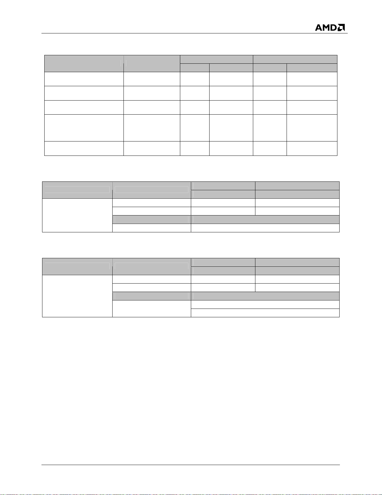
45215 Rev. 1.60 November 09
AMD SB710 Databook
Pin Name Voltage
SDA0/GPOC1#
SCL1/GPOC2# S5_3.3V -0.5 0.3* S5_3.3V
SDA1/GPOC3# S5_3.3V -0.5 0.3* S5_3.3V
IMC_GPIO[17:16, 12:11, 3],
PS2KB_DAT, PS2KB_CLK,
PS2M_DAT, PS2M_CLK,
PS2_DAT, PS2_CLK
IMC_GPIO[15:13, 10, 2]
KSO_[17:0], KSI_[7:0]
3.3 V
(5-V Tolerance)
S5_3.3V
(5-V Tolerance)
S5_3.3V -0.5 0.3* S5_3.3V
Table 11-5: GPIO/GEVENT Output DC Characteristics
ViL(V) ViH (V)
Min Max Min Max
-0.5 0.3* VDDQ 0.7*VDDQ V5_Ref + 0.25
-0.5 0.3* S5_3.3V
0.7*
S5_3.3V
0.7*
S5_3.3V
0.7*
S5_3.3V
0.7*
S5_3.3V
S5_3.3V + 0.25
S5_3.3V + 0.25
S5_3.3V + 0.25
V5_Ref + 0.25
Pin Name Parameter
Output High Voltage
All GPIO and GEVENT
pins listed in Table 11-4
Output Low Voltage
Output Drive
Table 11-6: RTC Clock Output DC Characteristics
Pin Name Parameter
Output High Voltage
Output Low Voltage
RTCCLK
Output Drive
VOL VOH
Minimum Maximum
2.4 V —
— 0.4 V
Output Drive
8 mA
VOL VOH
Minimum Maximum
2.4 V —
— 0.4 V
Output Drive
4 mA Min / 8 mA Max
Output drive controlled by PMIO 42 [6]
Electrical Characteristics 71
Page 72

AMD SB710 Databook
45215 Rev. 1.60 November 09
11.4 Reset Signal Requirements
Table 11-7: Reset Signal Requirements
Pin Name Assertion requirements Comments
At deassertion, the SYS_RST#
signal will not be sampled by the
SYS_RST# Must be asserted for 10ms minimum.
RSMRST# Must be asserted for 10ms minimum.
Must be asserted for 30 ns minimum.
internal logic for a period of 32 ms
as it first goes through the internal
debouncing circuit.
At deassertion, the RSMRST# signal
will not be sampled by the internal
logic for a period of 32 ms as it first
goes through the internal
debouncing circuit.
KBRST#
The KBRST# should be de-asserted
before A_RST# and LDT_RST# are deasserted.
—
11.5 RTC Battery Current Consumption
The RTC battery current consumption is estimated as follows:
Table 11-8: RTC Battery Current Consumption
Power State
G3 (Off) < 0.5 µA < 4 µA
S0-S5 < 0.2 µA -
RTC battery life is calculated using the rated capacity of the battery and typical current numbers. The
typical batteries used for RTC are normally rated for 170 mAh and the worst case current consumption for
the SB710 is 4.0 µA. Thus, the life of battery will be calculated as follows:
170,000 µAh / 4 µA = 42,500 h = 4.8 years
Typical Maximum
RTC Battery Current
72 Electrical Characteristics
Page 73

45215 Rev. 1.60 November 09
12 Package Information
12.1 Physical Dimensions
AMD SB710 Databook
Figure 12-1: SB710 21 mm x 21 mm 0.8 mm Pitch 528-FCBGA Package Outline
Table 12-1: SB710 21 mm x 21 mm 0.8 mm Pitch 528-FCBGA Physical Dimensions
Ref. Min(mm) Nominal (mm) Max. (mm)
c 0.56 0.66 0.76
A 1.77 1.92 2.07
A1 0.30 0.40 0.50
A2 0.81 0.86 0.91
b
D1 20.85 21.00 21.15
D2 - 6.47 D3 2.00 - D4 1.00 - E1 20.85 21.00 21.15
E2 - 6.68 E3 2.00 - E4 1.00 - F1 - 19.20 F2 - 19.20 -
e (min. pitch) - 0.80 -
ddd - - 0.20
Note: Maximum height of SMT components is 0.650 mm.
0.40 0.50 0.60
MOD-00067-RevA-p1
Package Information 73
Page 74

AMD SB710 Databook
45215 Rev. 1.60 November 09
12.2 Pressure Specification
To avoid damages to the ASIC (die or solder ball joint cracks) caused by improper mechanical assembly
of the cooling device, follow the recommendations below:
It is recommended that the maximum load that is evenly applied across the contact area between the
thermal management device and the die does not exceed 6 lbf. Note that a total load of 4-6 lbf is
adequate to secure the thermal management device and achieve the lowest thermal contact
resistance with a temperature drop across the thermal interface material of no more than 3°C. Also,
the surface flatness of the metal spreader should be 0.001 inch/1 inch.
Pre-test the assembly fixture with a strain gauge to make sure that the flexing of the final assembled
board and the pressure applying around the ASIC package will not exceed 600 micron strain under
any circumstances.
Ensure that any distortion (bow or twist) of the board after SMT and cooling device assembly is within
industry guidelines (IPC/EIA J-STD-001). For measurement method, refer to the industry approved
technique described in the manual IPC-TM-650, section 2.4.22.
13 Thermal Information
This section describes some key thermal parameters of the SB710. For a detailed discussion on
these parameters and other thermal design descriptions including package level thermal data and
analysis, please consult the Thermal Design and Analysis Guidelines for SB700/SB710/SB750.
Table 13-1 SB710 Thermal Limits
Parameter Minimum Nominal Maximum Unit Note
Operating Case
Temperature
Absolute Rated Junction
Temperature
Storage Temperature -40 — 60
Ambient Temperature 0 — 45
Thermal Design Power — 4.5 — W 4
0 — 105
— — 125
°
C 1
°
C 2
°
C
°
C 3
Notes:
1 - The maximum operating case temperature is the die geometric top-center temperature measured through proper
thermal contact to the back side of the die based on the methodology given in the document Thermal Design and
Analysis Guidelines for SB700/SB710/SB750 (Chapter 11). This is the temperature at which the functionality of the
chip is qualified.
2 - The maximum absolute rated junction temperature is the junction temperature at which the device can operate
without causing damage to the ASIC.
3 - The ambient temperature is defined as the temperature of the local intake air to the thermal management device.
The maximum ambient temperature is dependent on the heat sink's local ambient conditions as well as the chassis'
external ambient, and the value given here is based on AMD’s reference desktop heat sink solution for the SB710.
Refer to Chapter 5 in the Thermal Design and Analysis Guidelines for SB700/SB710/SB750 for heat sink and thermal
design guidelines. Refer to Chapter 6 of the above mentioned document for details of ambient conditions.
4 - Thermal Design Power (TDP) is defined as the highest power dissipated while running currently available worst
case applications at nominal voltages. The core voltage was raised to 5% above its nominal value for measuring the
ASIC power. Since the core power of modern ASICs using 65nm and smaller process technology can vary
significantly, parts specifically screened for higher core power were used for TDP measurement. The TDP is intended
only as a design reference, and the value given here is preliminary.
74 Thermal Information
Page 75
45215 Rev. 1.60 November 09
AMD SB710 Databook
14 Testability
14.1 Test Control Signals
Table 14-1 below shows the signals used for the integrated test controller of the SB710.
Table 14-1: Signals for the Test Controller of the SB710
Signal Name Description
14M_X1 / 14M_X2 25-MHz Reference Clock.
TEST0 Test0 input.
TEST1 Test1 input.
TEST2 Test2 input.
Table 14-2 shows how Test[2:0] are used to select the norm
Table 14-2: Test Mode Signals
TEST2 TEST1 TEST0 Test Mode Description
0 0 0 None Normal operation
0 0 1 Reserved Reserved for ASIC debug
0 1 x Test Mode EnableTest Mode
1 X X Reserved Reserved for ASIC debug
When TEST2 is low, a low on TEST1 will reset all test logic and allow TEST0 to choose between normal
operation and the reserved debug mode. A high on TEST1 should be followed by a bit sequence on
TEST0 to define the test mode into which the SB710 will enter. A new test mode can be entered when a
new bit sequence is transmitted. In addition to resetting the test controller asynchronously with TEST1, a
bit sequence can also be used to synchronously change the test mode. Table 14-3 sh
sequences for TEST0. Note: Once the Test mode or Test mode and sub test mode is entered, Test2 and
Test1 should be kept at 0, 1 respectively until the requirement for the Test Mode is completed.
al operation, ASIC debug, or test mode.
ows the
legal bit
Table 14-3: TEST0 Bit Sequence
TEST0 bit sequence Test Mode
11111 Look for first 0 to define a new test mode
00000 Reserved
00001 Alt Pull High Test
00010 Pull Outputs High
00011 Pull Outputs Low
00100 Pull Outputs to Z
00101 XOR Test Mode
Figure 14-1 illustrates the data timing for the test signals with respect to the OSC clock. Any timing
c
referen
e referred in this section is assumed to be based on OSC clock running at 25 MHz. The OSC
clock can be slowed down to 1 MHz as long as the bit stream applied on TEST0 pin is also in sync with
this clock. The 25-MHz OSC clock should be disconnected first. For setting any Test 0 bit sequence, the
OSC clock is required only up-to the time the mode set is completed. After this the clock can be stopped
Testability 75
Page 76

AMD SB710 Databook
45215 Rev. 1.60 November 09
and as long as TEST1 and Test2 pins are set to {1, 0} respectively to maintain the selected mode to be
active. Note that once TEST1 is set to one, TEST0 needs to be asserted to one for at least 8 clocks
before transmitting the test mode bit sequence. The rising of “Internal Test Mode” in the diagram indicates
the time when the SB710 enters into test mode.
Osc
TEST1
TEST0
( TEST0 = 1 ) >
8 Osc clocks
Internal Test Mode
Bit 4 Bit 1 Bit 2 Bit 3
Figure 14-1: Test Mode Capturing Sequence Timing
14.2 XOR Chain Test Mode
14.2.1 Brief Description of an XOR Chain
A sample of a generic XOR chain is shown in the figure below.
XOR Start Signal
G
F
E
Figure 14-2: A Generic XOR Chain
Bit 0
A
D
C
B
Pin A is assigned to the output direction, and pins B through F are assigned to the input direction.
It can be seen that after all pins from B to F are assigned to logic 0 or 1, a logic change in any
one of these pins will toggle the output pin A.
The following is the truth table for the XOR Chain shown in Figure 14-2. T
assumed to be logic 1.This is an internal signal to the ASIC and is not part of the XOR tree pins
listed in Table 14-5.
Once the inputs are
200 n
s. Note: OSC clock is not required to be running after the mode is already set and the pads
set to the respective value the output pin will reflect the correct value within
are exercised in XOR Tree function.
76 Testability
h
e XOR start signal is
Page 77

45215 Rev. 1.60 November 09
p
3
Table 14-4: Truth Table for an XOR Chain
Test Vector
number
1 0 0 0 0 0 0 1
2 1 0 0 0 0 0 0
3 1 1 0 0 0 0 1
4 1 1 1 0 0 0 0
5 1 1 1 1 0 0 1
6 1 1 1 1 1 0 0
7 1 1 1 1 1 1 1
14.2.2 Description of the SB710 XOR Chain
During XOR Chain Test Mode, most of the chip pads on the SB710 are connected together using
XOR gates as shown in Figure 14-3. The first input of the chain is connected to a logic level high
(internal connection
last pad in the chai
and
as well as and their order of connection. Pads are chained together in the shown order, i.e., pad
number 1 is the first pad on the XOR chain, pad number 2 the second, and so on.
Input Pin G Input Pin F Input Pin E Input Pin D Input Pin C Input Pin B Output Pin A
), and all pads (listed in Table 14-5) are configured as inputs except for the
n, which is configured as an output.
SERIRQ is the end of the chain. Table 14-5 lists all pads that are on the SB710 XOR chain,
AMD SB710 Databook
KBRST#/GEVENT1# is the start of the chain
1 ( Tie high Internal to Asic)
XOR out
FANOUT0/ GPIO3
pin 1
AD6/ROMA12
pin 2
in
pin N
Frame#
Figure 14-3: On-chip XOR Chain connectivity
Table 14-5: List of Pins on the SB710 XOR Chain and the Order of Connection
XOR # Pin Name
1
KBRST#/GEVENT1#
2
GA20IN/GEVENT0#
3
NB_PWRGD
4
SATA_ACT#/GPIO67
5
LDRQ1#/GNT5#/GPIO68
6
AD20
7
CBE2#
8
REQ2#
9
BMREQ#/REQ5#/GPIO65
10
REQ4#/GPIO71
11
GNT3#/GPIO72
XOR # Pin Name
12
CLKRUN#
13
REQ3#/GPIO70
14
GNT4#/GPIO73
15
INTF#/GPIO34
16
REQ1#
17
GNT1#
18
INTE#/GPIO33
19
INTH#/GPIO36
20
GNT0#
21
INTG#/GPIO35
22
AD31
Testability 77
Page 78

AMD SB710 Databook
XOR # Pin Name
23
GNT2#
24
REQ0#
25
AD29
26
AD30
27
AD25
28
AD27
29
AD28
30
FRAME#
31
IRDY#
32
AD24
33
AD26
34
AD19
35
AD16
36
TRDY#
37
AD21
38
AD22
39
AD23
40
CBE3#
41
AD17
42
STOP#
43
DEVSEL#
44
PERR#
45
CBE0#
46
AD9
47
AD18
48
SERR#
49
LOCK#
50
AD2
51
AD4
52
AD7
53
AD6
54
AD14
55
CBE1#
56
PAR
57
AD15
58
AD0
59
AD5
60
AD10
61
PCICLK4
62
PCICLK5/GPIO41
63
AD8
64
AD3
65
AD12
66
AD11
67
AD13
68
AD1
69
PCICLK0
XOR # Pin Name
70
PCICLK1
71
PCICLK3
72
PCICLK2
73
FANIN2/GPIO52
74
FANIN1/GPIO51
75
FANIN0/GPIO50
76
FANOUT0/GPIO3
77
FANOUT2/GPIO49
78
FANOUT1/GPIO48
79
AZ_SDOUT
80
AZ_BITCLK
81
AZ_SYNC
82
A_RST#
83
AZ_SDIN3/GPIO46
84
PCIRST#
85
AZ_RST#
86
AZ_SDIN2/GPIO44
87
AZ_DOCK_RST#/GPM8#
88
LPC_PME#/GEVENT3#
89
SUS_STAT#
90
SDA1/GPOC3#
91
SCL1/GPOC2#
92
AZ_SDIN1/GPIO43
93
AZ_SDIN0/GPIO42
SMBALERT#/THRMTRIP#/
94
GEVENT2#
95
SYS_RESET#/GPM7#
96
ROM_RST#/GPIO14
97
SLP_S2/GPM9#
98
WAKE#/GEVENT8#
99
PWR_BTN#
100
SPI_DI/GPIO12
101
DDR3_RST#/GEVENT7#
102
SPI_HOLD#/GPIO31
103
SPI_CS1#/GPIO32
104
SPI_DO/GPIO11
105
S3_STATE/GEVENT5#
106
RI#/EXTEVNT0#
107
PCI_PME#/GEVENT4#
108
BLINK/GPM6#
109
SPI_CLK/GPIO47
110
LLB#/GPIO66
111
USB_OC0#/GPM0#
112
USB_OC1#/GPM1#
113
USB_FSDP13+/-
114
USB_FSDP12+/-
115
VIN3/GPIO56
45215 Rev. 1.60 November 09
78 Testability
Page 79

45215 Rev. 1.60 November 09
XOR # Pin Name
116
VIN4/GPIO57
117
VIN2/GPIO55
118
VIN1/GPIO54
119
VIN0/GPIO53
120
VIN7/GPIO60
121
VIN6/GPIO59
122
VIN5/GPIO58
123
TEMPIN3/TALERT#/GPIO64
124
TEMPIN2/GPIO63
125
TEMPIN1/GPIO62
126
TEMPIN0/GPIO61
127
USB_OC2#/GPM2#
128
USB_OC3#/GPM3#
129
USB_OC4#/IR_RX/GPM4#
130
USB_OC5#/IR_TX/GPM5#
USB_OC6#/IR_CTRL/
131
GEVENT6#
USBCLK/
132
14M_25M_48M_OSC
133
IMC_GPO17
134
KSO_14
135
KSO_15
136
KSO_17
137
KSO_16
138
IMC_GPIO12
139
IMC_GPIO15
140
IMC_GPO16
141
KSO_12
142
KSO_13
143
KSI_0
144
IMC_GPIO13
145
KSO_8
146
KSO_9
147
KSO_11
148
KSO_10
149
KSI_1
150
IMC_GPIO10
151
IMC_GPIO14
152
IMC_GPIO11
153
KSO_6
154
KSO_7
155
PS2_DAT
156
LDT_PG
157
PS2_CLK
158
PS2KB_DAT
159
KSO_3
160
KSO_5
XOR # Pin Name
161
KSO_4
162
PS2M_CLK
163
KSI_7
164
KSO_1
165
KSO_2
166
KSO_0
167
KSI_6
168
KSI_5
169
KSI_4
170
KSI_3
171
KSI_2
172
PS2KB_CLK
173
PS2M_DAT
IDE_RST#/F_RST#/
174
IMC_GPO3
175
ALLOW_LDTSTP
176
PROCHOT#
177
LDT_STP#
178
LDT_RST#
179
LPCCLK1
180
LPCCLK0
181
SPI_CS2#/IMC_GPIO2
182
LDRQ0#
183
LAD1
184
LAD0
185
LFRAME#
186
LAD2
187
LAD3
188
LPC_SMI#/EXTEVNT1#
189
SDA0/GPOC1#
CLK_REQ2#/SATA_IS5#/
190
FANIN3/GPIO40
191
SPKR/GPIO2
192
DDC1_SDA/GPIO8
SMARTVOLT2/SHUTDOWN#/
193
GPIO5
194
DDC1_SCL/GPIO9
SMARTVOLT1/SATA_IS2#/
195
GPIO4
196
IDE_A2
197
IDE_A0
198
IDE_CS3#
199
IDE_CS1#
200
IDE_IORDY
201
IDE_IRQ
202
IDE_D12/GPIO27
203
IDE_DACK#
204
IDE_A1
AMD SB710 Databook
Testability 79
Page 80

AMD SB710 Databook
XOR # Pin Name
205
IDE_D15/GPIO30
206
IDE_IOW#
207
IDE_IOR#
208
IDE_D3/GPIO18
209
IDE_D1/GPIO16
210
IDE_D0/GPIO15
211
IDE_DRQ
212
IDE_D14/GPIO29
213
IDE_D2/GPIO17
214
IDE_D13/GPIO28
215
IDE_D11/GPIO26
216
IDE_D4/GPIO19
217
IDE_D9/GPIO24
218
IDE_D6/GPIO21
219
IDE_D5/GPIO20
220
IDE_D10/GPIO25
221
IDE_D8/GPIO23
222
IDE_D7/GPIO22
223
SATA_IS0#/GPIO10
CLK_REQ3#/SATA_IS1#/
224
GPIO6
225
SCL0/GPOC0#
CLK_REQ0#/SATA_IS3#/
226
GPIO0
CLK_REQ1#/SATA_IS4#/
227
FANOUT3/GPIO39
228
LAN_RST#/GPIO13
229
SERIRQ
45215 Rev. 1.60 November 09
80 Testability
Page 81

45215 Rev. 1.60 November 09
AMD SB710 Databook
14.2.2.1 Unused Pins
The pins that are part of the XOR chain (see Table 14-5) but are not used for testing must be pulled-up or
down before the XOR
analog pins not included in Table 14-5 are not part of the XOR chai
XOR test. That includes the output of the XOR chain, FANOUT0/GPIO3, and other pads shown in Table
14-6 belo
w.
Table 14-6: Pins Excluded from the XOR Chain
Pin Name Description
RSMRST# Used for capturing straps
PWR_GOOD Used for capturing straps
SLP_S5# In S5 power well. No test support.
SLP_S3# In S5 power well. No test support.
SIC No test support
TEST0 Test controller data input
TEST1 Test controller mode
TEST2 Reserved Test Input
14M_X1 Test control clock
14M_X2 Test control clock
RTCCLK No test support
SERIRQ Output of the XOR chain
n is activated. No pins in the XOR chain should be left floating. All digital or
chai
n and can be
left floating during an
Testability 81
Page 82

AMD SB710 Databook
Appendix A: Pin Listing
45215 Rev. 1.60 November 09
Processor Interface
ALLOW_LDTSTP
LDT_PG
LDT_STP#
LDT_RST#
PROCHOT#
LPC Interface
LPCCLK0
LPCCLK1
LAD0
LAD1
LAD2
LAD3
LFRAME#
LDRQ0#
LDRQ1#/GNT5#/GPIO68
LPC_SMI#/EXTEVNT1#
SERIRQ
A-Link Express II Interface
PCIE_RCLKP/NB_LNK_CLKP
PCIE_RCLKN/NB_LNK_CLKN
PCIE_TX0P
PCIE_TX0N
PCIE_TX1P
PCIE_TX1N
PCIE_TX2P
PCIE_TX2N
PCIE_TX3P
PCIE_TX3N
PCIE_RX0P
PCIE_RX0N
PCIE_RX1P
PCIE_RX1N
PCIE_RX2P
PCIE_RX2N
PCIE_RX3P
PCIE_RX3N
PCIE_CALRP
PCIE_CALRN
PCI 33 Interface
PCICLK0
PCICLK1
PCICLK2
PCICLK3
PCICLK4
F23
F22
G25
G24
F24
G22
E22
H24
H23
J25
J24
H25
H22
AB8
K24
V15
N25
N24
V23
V22
V24
V25
U25
U24
T23
T22
U22
U21
U19
V19
R20
R21
R18
R17
T25
T24
P4
P3
P1
P2
T4
PCICLK5/GPIO41
A_RST#
PCIRST#
INTE#/GPIO33
INTF#/GPIO34
INTG#/GPIO35
INTH#/GPIO36
AD0
AD1
AD2
AD3
AD4
AD5
AD6
AD7
AD8
AD9
AD10
AD11
AD12
AD13
AD14
AD15
AD16
AD17
AD18
AD19
AD20
AD21
AD22
AD23
AD24
AD25
AD26
AD27
AD28
AD29
AD30
AD31
CBE0#
CBE1#
CBE2#
CBE3#
FRAME#
DEVSEL#
IRDY#
T3
N2
N1
AD3
AC4
AE2
AE3
U2
P7
V4
T1
V3
U1
V1
V2
T2
W1
T9
R6
R7
R5
U8
U5
Y7
W8
V9
Y8
AA8
Y4
Y3
Y2
AA2
AB4
AA1
AB3
AB2
AC1
AC2
AD1
W2
U7
AA7
Y1
AA6
W5
AA5
82 Appendix A: Pin Listing
Page 83

45215 Rev. 1.60 November 09
TRDY#
PAR
STOP#
PERR#
SERR#
LOCK#
REQ0#
REQ1#
REQ2#
REQ3#/GPIO70
REQ4#/GPIO71
BMREQ#/REQ5#/GPIO65
GNT0#
GNT1#
GNT2#
GNT3#/GPIO72
GNT4#/GPIO73
LDRQ1#/GNT5#/GPIO68
CLKRUN#
USB Interface
USB_FSD13P
USB_FSD13N
USB_FSD12P
USB_FSD12N
USB_HSD11P
USB_HSD11N
USB_HSD10P
USB_HSD10N
USB_HSD9P
USB_HSD9N
USB_HSD8P
USB_HSD8N
USB_HSD7P
USB_HSD7N
USB_HSD6P
USB_HSD6N
USB_HSD5P
USB_HSD5N
USB_HSD4P
USB_HSD4N
USB_HSD3P
USB_HSD3N
USB_HSD2P
USB_HSD2N
USB_HSD1P
USB_HSD1N
USB_HSD0P
Y5
U6
W6
W4
V7
V5
AC3
AD4
AB7
AE6
AB6
AD7
AD2
AE4
AD5
AC6
AE5
AB8
AD6
E6
E7
F7
E8
H11
J10
E11
F11
A11
B11
C10
D10
G11
H12
E12
E14
C12
D12
B12
A12
G12
G14
H14
H15
A13
B13
B14
USB_HSD0N
USBCLK/14M_25M_48M_OSC
USB_RCOMP
ATA66/100/133
IDE_RST#/F_RST#/IMC_GPO3
IDE_IORDY
IDE_IRQ
IDE_A0
IDE_A1
IDE_A2
IDE_DACK#
IDE_DRQ
IDE_IOR#
IDE_IOW#
IDE_CS1#
IDE_CS3#
IDE_D0/GPIO15
IDE_D1/GPIO16
IDE_D2/GPIO17
IDE_D3/GPIO18
IDE_D4/GPIO19
IDE_D5/GPIO20
IDE_D6/GPIO21
IDE_D7/GPIO22
IDE_D8/GPIO23
IDE_D9/GPIO24
IDE_D10/GPIO25
IDE_D11/GPIO26
IDE_D12/GPIO27
IDE_D13/GPIO28
IDE_D14/GPIO29
IDE_D15/GPIO30
Serial ATA
SATA_TX0P
SATA_TX0N
SATA_RX0N
SATA_RX0P
SATA_TX1P
SATA_TX1N
SATA_RX1N
SATA_RX1P
SATA_TX2P
SATA_TX2N
SATA_RX2N
SATA_RX2P
SATA_TX3P
SATA_TX3N
SATA_RX3N
AMD SB710 Databook
A14
C8
G8
F25
AA24
AA25
Y22
AB23
Y23
AB24
AD25
AC25
AC24
Y25
Y24
AD24
AD23
AE22
AC22
AD21
AE20
AB20
AD19
AE19
AC20
AD20
AE21
AB22
AD22
AE23
AC23
AD9
AE9
AB10
AC10
AE10
AD10
AD11
AE11
AB12
AC12
AE12
AD12
AD13
AE13
AB14
Appendix A: Pin Listing 83
Page 84

AMD SB710 Databook
SATA_RX3P
SATA_TX4P
SATA_TX4N
SATA_RX4N
SATA_RX4P
SATA_TX5P
SATA_TX5N
SATA_RX5N
SATA_RX5P
SATA_CAL
SATA_X1
SATA_X2
SATA_ACT#/GPIO67
SATA_IS0#/GPIO10
SMARTVOLT1/SATA_IS2#/
GPIO4
CLK_REQ0#/SATA_IS3#/
GPIO0
CLK_REQ1#/SATA_IS4#/
FANOUT3/GPIO39
CLK_REQ2#/SATA_IS5#/
FANIN3/GPIO40
CLK_REQ3#/SATA_IS1#/
GPIO6
HD Audio Interface
AZ_BITCLK
AZ_SDOUT
AZ_SYNC
AZ_RST#
AZ_SDIN0/GPIO42
AZ_SDIN1/GPIO43
AZ_SDIN2/GPIO44
AZ_SDIN3/GPIO46
Real Time Clock
X1
X2
VBAT
RTCCLK
INTRUDER_ALERT#
Clocks
14M_X1
14M_X2
USBCLK/14M_25M_48M_OSC
25M_48M_66M_OSC
PCIE_RCLKP/NB_LNK_CLKP
PCIE_RCLKN/NB_LNK_CLKN
NB_DISP_CLKP
NB_DISP_CLKN
NB_HT_CLKP
AC14
AE14
AD14
AD15
AE15
AB16
AC16
AE16
AD16
V12
Y12
AA12
W11
AE18
AA19
W17
V17
W20
AD18
M1
M2
L6
M4
J7
J8
L8
M3
A3
B3
B2
C3
C2
J21
J20
C8
L18
N25
N24
K23
K22
M24
NB_HT_CLKN
CPU_HT_CLKP
CPU_HT_CLKN
SLT_GFX_CLKP
SLT_GFX_CLKN
GPP_CLK0P
GPP_CLK0N
GPP_CLK1P
GPP_CLK1N
GPP_CLK2P
GPP_CLK2N
GPP_CLK3P
GPP_CLK3N
Hardware Monitor
FANOUT0/GPIO3
FANOUT1/GPIO48
FANOUT2/GPIO49
CLK_REQ1#/SATA_IS4#/
FANOUT3/GPIO39
FANIN0/GPIO50
FANIN1/GPIO51
FANIN2/GPIO52
CLK_REQ2#/SATA_IS5#/
FANIN3/GPIO40
TEMP_COMM
TEMPIN0/GPIO61
TEMPIN1/GPIO62
TEMPIN2/GPIO63
TEMPIN3/TALERT#/GPIO64
VIN0/GPIO53
VIN1/GPIO54
VIN2/GPIO55
VIN3/GPIO56
VIN4/GPIO57
VIN5/GPIO58
VIN6/GPIO59
VIN7/GPIO60
AVDD
AVSS
SPI ROM Interface
SPI_DI/GPIO12
SPI_DO/GPIO11
SPI_CLK/GPIO47
SPI_HOLD#/GPIO31
SPI_CS1#/GPIO32
SPI_CS2#/IMC_GPIO2
45215 Rev. 1.60 November 09
M25
P17
M18
M23
M22
J19
J18
L20
L19
M19
M20
N22
P22
M8
M5
M7
V17
P5
P8
R8
W20
C6
B6
A6
A5
B5
A4
B4
C4
D4
D5
D6
A7
B7
F6
G7
G6
D2
D1
F4
F3
H21
84 Appendix A: Pin Listing
Page 85

45215 Rev. 1.60 November 09
NB / Power Mgmt
SLP_S2/GPM9#
SLP_S3#
SLP_S5#
PWR_BTN#
PWR_GOOD
SUS_STAT#
TEST0
TEST1
TEST2
Integrated Micro-controller
PS2_DAT
PS2_CLK
SPI_CS2#/IMC_GPIO2
IDE_RST#/F_RST#/IMC_GPO3
PS2KB_DAT
PS2KB_CLK
PS2M_DAT
PS2M_CLK
KSO_16
KSO_17
IMC_PWM0/IMC_GPIO10
SCL2/IMC_GPIO11
SDA2/IMC_GPIO12
SCL3_LV/IMC_GPIO13
SDA3_LV/IMC_GPIO14
IMC_PWM1/IMC_GPIO15
IMC_PWM2/IMC_GPO16
IMC_PWM3/IMC_GPO17
KSI_0
KSI_1
KSI_2
KSI_3
KSI_4
KSI_5
KSI_6
KSI_7
KSO_0
KSO_1
KSO_2
KSO_3
KSO_4
KSO_5
KSO_6
KSO_7
KSO_8
H7
F5
G1
H2
H1
K3
H3
H4
H5
H19
H20
H21
F25
D22
E24
E25
D23
A18
B18
F21
D21
F19
E20
E21
E19
D19
E18
G20
G21
D25
D24
C25
C24
B25
C23
B24
B23
A23
C22
A22
B22
B21
A21
D20
KSO_9
KSO_10
KSO_11
KSO_12
KSO_13
KSO_14
KSO_15
General Events
RI#/EXTEVNT0#
LPC_SMI#/EXTEVNT1#
GA20IN/GEVENT0#
KBRST#/GEVENT1#
SMBALERT#/THRMTRIP#/
GEVENT2#
LPC_PME#/GEVENT3#
PCI_PME#/GEVENT4#
S3_STATE/GEVENT5#
USB_OC6#/IR_TX1/GEVENT6#
DDR3_RST#/GEVENT7#
WAKE#/GEVENT8#
USB_OC0#/GPM0#
USB_OC1#/GPM1#
USB_OC2#/GPM2#
USB_OC3#/IR_RX1/GPM3#
USB_OC4#/IR_RX0/GPM4#
USB_OC5#/IR_TX0/GPM5#
BLINK/GPM6#
SYS_RESET#/GPM7#
AZ_DOCK_RST#/GPM8#
SLP_S2/GPM9#
SM Bus
SCL0/GPOC0#
SDA0/GPOC1#
SCL1/GPOC2#
SDA1/GPOC3#
SCL2/IMC_GPIO11
SDA2/IMC_GPIO12
SCL3_LV/IMC_GPIO13
SDA3_LV/IMC_GPIO14
General Purpose I/O
CLK_REQ0#/SATA_IS3#/
GPIO0
SPKR/GPIO2
FANOUT0/GPIO3
SMARTVOLT1/SATA_IS2#/
GPIO4
SMARTVOLT2/SHUTDOWN#/
GPIO5
AMD SB710 Databook
C20
A20
B20
B19
A19
D18
C18
E2
K24
Y15
W15
J6
K4
E1
F1
B9
G5
H6
E4
F8
E5
A9
A8
B8
F2
J2
L5
H7
AA18
W18
K1
K2
D21
F19
E20
E21
W17
W21
M8
AA19
Y19
Appendix A: Pin Listing 85
Page 86

AMD SB710 Databook
CLK_REQ3#/SATA_IS1#/
GPIO6
NB_PWRGD
DDC1_SDA/GPIO8
DDC1_SCL/GPIO9
SATA_IS0#/GPIO10
SPI_DO/GPIO11
SPI_DI/GPIO12
LAN_RST#/GPIO13
ROM_RST#/GPIO14
IDE_D0/GPIO15
IDE_D1/GPIO16
IDE_D2/GPIO17
IDE_D3/GPIO18
IDE_D4/GPIO19
IDE_D5/GPIO20
IDE_D6/GPIO21
IDE_D7/GPIO22
IDE_D8/GPIO23
IDE_D9/GPIO24
IDE_D10/GPIO25
IDE_D11/GPIO26
IDE_D12/GPIO27
IDE_D13/GPIO28
IDE_D14/GPIO29
IDE_D15/GPIO30
SPI_HOLD#/GPIO31
SPI_CS1#/GPIO32
INTE#/GPIO33
INTF#/GPIO34
INTG#/GPIO35
INTH#/GPIO36
SERIRQ
CLK_REQ1#/SATA_IS4#/
FANOUT3/GPIO39
CLK_REQ2#/SATA_IS5#/
FANIN3/GPIO40
PCICLK5/GPIO41
AZ_SDIN0/GPIO42
AZ_SDIN1/GPIO43
AZ_SDIN2/GPIO44
AZ_SDIN3/GPIO46
SPI_CLK/GPIO47
FANOUT1/GPIO48
AD18
W14
Y18
AA20
AE18
D2
G6
U15
J1
AD24
AD23
AE22
AC22
AD21
AE20
AB20
AD19
AE19
AC20
AD20
AE21
AB22
AD22
AE23
AC23
F4
F3
AD3
AC4
AE2
AE3
V15
V17
W20
T3
J7
J8
L8
M3
D1
M5
FANOUT2/GPIO49
FANIN0/GPIO50
FANIN1/GPIO51
FANIN2/GPIO52
VIN0/GPIO53
VIN1/GPIO54
VIN2/GPIO55
VIN3/GPIO56
VIN4/GPIO57
VIN5/GPIO58
VIN6/GPIO59
VIN7/GPIO60
TEMPIN0/GPIO61
TEMPIN1/GPIO62
TEMPIN2/GPIO63
TEMPIN3/TALERT#/GPIO64
BMREQ#/REQ5#/GPIO65
LLB#/GPIO66
SATA_ACT#/GPIO67
LDRQ1#/GNT5#/GPIO68
REQ3#/GPIO70
REQ4#/GPIO71
GNT3#/GPIO72
GNT4#/GPIO73
Reset
RSMRST#
SYS_RESET#/GPM7#
Special Power
V5_VREF
AVDDCK_3.3V
AVDDCK_1.2V
AVSSCK
CKVDD_1.2V_1
CKVDD_1.2V_2
CKVDD_1.2V_3
CKVDD_1.2V_4
USB Analog Power
AVDDTX_0
AVDDTX_1
AVDDTX_2
AVDDTX_3
AVDDTX_4
AVDDTX_5
45215 Rev. 1.60 November 09
M7
P5
P8
R8
A4
B4
C4
D4
D5
D6
A7
B7
B6
A6
A5
B5
AD7
C1
W11
AB8
AE6
AB6
AC6
AE5
D3
J2
AE7
J16
K17
L17
L21
L22
L24
L25
A16
B16
C16
D16
D17
E17
86 Appendix A: Pin Listing
Page 87

45215 Rev. 1.60 November 09
AVDDRX_0
AVDDRX_1
AVDDRX_2
AVDDRX_3
AVDDRX_4
AVDDRX_5
AVDDC
AVSSC
USB Analog Ground
AVSS_USB_1
AVSS_USB_2
AVSS_USB_3
AVSS_USB_4
AVSS_USB_5
AVSS_USB_6
AVSS_USB_7
AVSS_USB_8
AVSS_USB_9
AVSS_USB_10
AVSS_USB_11
AVSS_USB_12
AVSS_USB_13
AVSS_USB_14
AVSS_USB_15
AVSS_USB_16
AVSS_USB_17
AVSS_USB_18
AVSS_USB_19
AVSS_USB_20
AVSS_USB_21
AVSS_USB_22
AVSS_USB_23
AVSS_USB_24
PCI Express Analog Power
PCIE_PVDD
PCIE_VDDR_1
PCIE_VDDR_2
PCIE_VDDR_3
PCIE_VDDR_4
PCIE_VDDR_5
PCIE_VDDR_6
PCIE_VDDR_7
PCI-E & Other Analog Grounds
PCIE_CK_VSS_1
PCIE_CK_VSS_10
PCIE_CK_VSS_11
PCIE_CK_VSS_12
PCIE_CK_VSS_13
F15
F17
F18
G15
G17
G18
E9
F9
A15
B15
C14
D8
D9
D11
D13
D14
D15
E15
F12
F14
G9
H9
H17
J9
J11
J12
J14
J15
K10
K12
K14
K15
P24
P18
P19
P20
P21
R22
R24
R25
H18
R16
R19
T17
U18
PCIE_CK_VSS_14
PCIE_CK_VSS_15
PCIE_CK_VSS_16
PCIE_CK_VSS_17
PCIE_CK_VSS_18
PCIE_CK_VSS_19
PCIE_CK_VSS_2
PCIE_CK_VSS_20
PCIE_CK_VSS_21
PCIE_CK_VSS_3
PCIE_CK_VSS_4
PCIE_CK_VSS_5
PCIE_CK_VSS_6
PCIE_CK_VSS_7
PCIE_CK_VSS_8
PCIE_CK_VSS_9
PCIE_PVSS
Serial ATA Analog Power
AVDD_SATA_1
AVDD_SATA_2
AVDD_SATA_3
AVDD_SATA_4
AVDD_SATA_5
AVDD_SATA_6
AVDD_SATA_7
XTLVDD_SATA
PLLVDD_SATA
Serial ATA Analog Ground
AVSS_SATA_1
AVSS_SATA_2
AVSS_SATA_3
AVSS_SATA_4
AVSS_SATA_5
AVSS_SATA_6
AVSS_SATA_7
AVSS_SATA_8
AVSS_SATA_9
AVSS_SATA_10
AVSS_SATA_11
AVSS_SATA_12
AVSS_SATA_13
AVSS_SATA_14
AVSS_SATA_15
AVSS_SATA_16
AVSS_SATA_17
AVSS_SATA_18
AVSS_SATA_19
AVSS_SATA_20
AMD SB710 Databook
U20
V18
V20
V21
W19
W22
J17
W24
W25
J22
K25
M16
M17
M21
P16
P23
P25
AA14
AA15
AA17
AB18
AC18
AD17
AE17
W12
AA11
T10
U10
U11
U12
V11
V14
W9
Y9
Y11
Y14
Y17
AA9
AB9
AB11
AB13
AB15
AB17
AC8
AD8
AE8
Appendix A: Pin Listing 87
Page 88

AMD SB710 Databook
Core Power
VDD_1
VDD_2
VDD_3
VDD_4
VDD_5
VDD_6
VDD_7
VDD_8
VDD_9
3.3V I/O Power
VDDQ_1
VDDQ_2
VDDQ_3
VDDQ_4
VDDQ_5
VDDQ_6
VDDQ_7
VDDQ_8
VDDQ_9
VDDQ_10
VDDQ_11
VDDQ_12
IDE I/O Power
VDD33_18_1
VDD33_18_2
VDD33_18_3
VDD33_18_4
3.3V Standby Power
S5_3.3V_1
S5_3.3V_2
S5_3.3V_3
S5_3.3V_4
S5_3.3V_5
S5_3.3V_6
S5_3.3V_7
1.2V Standby Power
S5_1.2V_1
S5_1.2V_2
USB Phy Digital Power
USB_PHY_1.2V_1
USB_PHY_1.2V_2
Digital Ground
VSS_1
VSS_2
VSS_3
VSS_4
VSS_5
L15
M12
M14
N13
P12
P14
R11
R15
T16
L9
M9
T15
U9
U16
U17
V8
W7
Y6
AA4
AB5
AB21
Y20
AA21
AA22
AE25
A17
A24
B17
J4
J5
L1
L2
G2
G4
A10
B10
A2
A25
B1
D7
F20
VSS_6
VSS_7
VSS_8
VSS_9
VSS_10
VSS_11
VSS_12
VSS_13
VSS_14
VSS_15
VSS_16
VSS_17
VSS_18
VSS_19
VSS_20
VSS_21
VSS_22
VSS_23
VSS_24
VSS_25
VSS_26
VSS_27
VSS_28
VSS_29
VSS_30
VSS_31
VSS_32
VSS_33
VSS_34
VSS_35
VSS_36
VSS_37
VSS_38
VSS_39
VSS_40
VSS_41
VSS_42
VSS_43
VSS_44
VSS_45
VSS_46
VSS_47
VSS_48
VSS_49
VSS_50
45215 Rev. 1.60 November 09
G19
H8
K9
K11
K16
L4
L7
L10
L11
L12
L14
L16
M6
M10
M11
M13
M15
N4
N12
N14
P6
P9
P10
P11
P13
P15
R1
R2
R4
R9
R10
R12
R14
T11
T12
T14
U4
U14
V6
Y21
AB1
AB19
AB25
AE1
AE24
88 Appendix A: Pin Listing
 Loading...