

Page 1

AMD 780G Family
Register Programming Requirements
For the RS780, RS780C, RS780D, RS780M,
RS780E, RS780MC, and RX781
Technical Reference Manual
Rev. 1.01
P/N: 43291_rs780_rpr_pub_1.01
© 2009 Advanced Micro Devices, Inc.
Page 2

Trademarks
AMD, the AMD Arrow logo, AMD Athlon, ATI, Mobility, PowerPlay, CrossFire, Radeon, and combinations thereof, are trademarks of Advanced Micro Devices, Inc.
HyperTransport is a licensed trademark of the HyperTransport Technology Consortium.
Microsoft and Windows are registered trademarks of Microsoft Corporation.
Other product names used in this publication are for identification purposes only and may be trademarks of their respective companies.
Disclaimer
The contents of this document are provided in connection with Advanced Micro Devices, Inc. ("AMD") products. AMD makes no representations or warranties with respect
to the accuracy or completeness of the contents of this publication and reserves the right to make changes to specifications and product descriptions at any time without notice.
No license, whether express, implied, arising by estoppel, or otherwise, to any intellectual property rights are granted by this publication. Except as set forth in AMD's Standard
Terms and Conditions of Sale, AMD assumes no liability whatsoever, and disclaims any express or implied warranty, relating to its products including, but not limited to, the
implied warranty of merchantability, fitness for a particular purpose, or infringement of any intellectual property right.
AMD's products are not designed, intended, authorized or warranted for use as components in systems intended for surgical implant into the body, or in other applications
intended to support or sustain life, or in any other application in which the failure of AMD's product could create a situation where personal injury, death, or severe property or
environmental damage may occur. AMD reserves the right to discontinue or make changes to its products at any time without notice.
© 2009 Advanced Micro Devices, Inc. All rights reserved.
Page 3

Table of Contents
Chapter 1: Introduction
1.1 About This Manual .............................................................................................................................................................1-1
Chapter 2: I/O Control (IOC)
2.1 RS780 Device Mapping ......................................................................................................................................................2-1
2.2 RS780 Device IDs...............................................................................................................................................................2-1
2.3 Configuration Access to RS780 Device Registers..............................................................................................................2-2
2.3.1 Using CF8/CFC I/O Pair ......................................................................................................................................2-2
2.3.2 Using BAR3 Memory Mapped Register Access..................................................................................................2-2
2.4 General RS780 IOC Programming After Boot-Up.............................................................................................................2-3
2.5 Miscellaneous IOC Features Programming ........................................................................................................................2-4
2.5.1 Power Management Register Access Setup .........................................................................................................2-4
2.5.2 S3 PME_Turn_Off/PME_To_Ack Sequence.......................................................................................................2-4
2.5.3 Disabling Internal Graphics..................................................................................................................................2-4
2.5.4 GFX MSI Enable..................................................................................................................................................2-4
2.5.5 Disabling Bus0 Device 3 PCI Bridge (Secondary External PCIE Graphics).......................................................2-4
2.5.6 Disabling Bus0 Device 3 PCI Bridges (Dev2, Dev4 to Dev7, Dev9-Dev10) ......................................................2-4
2.6 Broadcast CPU Requests to Dual External Graphics PCIE Devices ..................................................................................2-5
2.7 Enabling/Disabling Peer-To-Peer Traffic Access...............................................................................................................2-6
2.8 Enabling/Disabling MVPU .................................................................................................................................................2-6
2.9 IOC Dynamic Clock Setup .................................................................................................................................................2-6
2.10 Interrupt Mapping .............................................................................................................................................................2-7
2.11 GSM Enable......................................................................................................................................................................2-7
Chapter 3: Clock Settings
3.1 SBIOS Memory Clock Initialization...................................................................................................................................3-1
3.1.1 UMA Mode ..........................................................................................................................................................3-1
3.1.2 Side-Port Async Mode .........................................................................................................................................3-1
3.2 Memory Clock Changes For POWERPLAY......................................................................................................................3-3
3.3 Switching Back From PM Mode to Nominal Mode ...........................................................................................................3-4
3.4 Power Saving Settings ........................................................................................................................................................3-5
3.4.1 Enabling Dynamic Clocks ...................................................................................................................................3-5
3.4.2 Powering Down Efuse and Strap Block Clocks After Boot-Up...........................................................................3-5
3.4.3 Powering Down Graphics Core and Memory Clocks in Northbridge-Only Mode ..............................................3-6
3.4.4 Powering Down IOC GFX Clock in No External Graphics Mode ......................................................................3-6
3.4.5 PWM Controller ...................................................................................................................................................3-6
3.5 DOS Mode Power Saving ...................................................................................................................................................3-7
3.6 HTPLL VCO Mode Setting ................................................................................................................................................3-7
Chapter 4: Memory Initialization
4.1 Memory Initialization .........................................................................................................................................................4-1
Chapter 5: PCIE Initialization
5.1 Introduction.........................................................................................................................................................................5-1
5.2 PCI Express Configuration Space.......................................................................................................................................5-1
5.2.1 PCIE Port Configuration Space............................................................................................................................5-1
© 2009 Advanced Micro Devices, Inc. AMD 780G Register Programming Requirements 1.01
Table of Contents-1
Page 4

Table of Contents
5.2.2 PCIE Core Index Space ....................................................................................................................................... 5-2
5.2.3 PCIE Port Index Space ........................................................................................................................................ 5-2
5.2.4 PCIE Extended Configuration Space................................................................................................................... 5-2
5.3 Power-On and Reset State.................................................................................................................................................. 5-4
5.4 PCIE GFX Configurations ................................................................................................................................................. 5-4
5.4.1 PCIE Modes Only................................................................................................................................................ 5-4
5.4.2 DDI Modes Only ................................................................................................................................................. 5-5
5.4.3 PCIE and DDI Combined Modes ........................................................................................................................ 5-6
5.5 PCIE GPPSB Configurations ............................................................................................................................................. 5-6
5.5.1 Device Remapping............................................................................................................................................... 5-7
5.5.2 Default Configuration E (STRAP_BIF_LINK_CONFIG_GPPSB = 4’b0100) .................................................. 5-7
5.5.3 Configuration A (STRAP_BIF_LINK_CONFIG_GPPSB = 4’b0000) .............................................................. 5-8
5.5.4 Configuration B (STRAP_BIF_LINK_CONFIG_GPPSB = 4’b0001)............................................................... 5-8
5.5.5 Configuration C (STRAP_BIF_LINK_CONFIG_GPPSB = 4’b0010)............................................................... 5-8
5.5.6 Configuration D (STRAP_BIF_LINK_CONFIG_GPPSB = 4’b0011) .............................................................. 5-8
5.5.7 Switching GPPSB Configurations....................................................................................................................... 5-9
5.6 PCIE GPP Configurations................................................................................................................................................ 5-10
5.6.1 Default Configuration D .................................................................................................................................... 5-10
5.6.2 Configuration C ................................................................................................................................................. 5-10
5.7 PCIE Link Training Sequence...........................................................................................................................................5-11
5.8 Overall PCIE Programming Sequence ............................................................................................................................. 5-13
5.9 PCIE-GFX Core Initialization.......................................................................................................................................... 5-14
5.9.1 REFCLK Options .............................................................................................................................................. 5-14
5.9.2 Lane Reversal (CMOS Option - Disabled by Default)...................................................................................... 5-15
5.9.3 GFX Overclocking............................................................................................................................................. 5-15
5.9.4 Reset PCIE-GFX Core....................................................................................................................................... 5-16
5.9.5 Reset PCIE-GFX Slot ........................................................................................................................................ 5-16
5.9.6 Delay Training Option (CMOS Option – Default 2ms) ................................................................................... 5-16
5.9.7 Transmitter Drive Strength (CMOS Option – Default 22mA) .......................................................................... 5-16
5.9.8 Program PCIE Memory Mapped Configuration Space ..................................................................................... 5-17
5.9.9 GEN1 Software Compliance (CMOS Option – Disabled by Default) .............................................................. 5-17
5.9.10 GEN2 Software Compliance (CMOS Option – Disabled by Default) .............................................................. 5-18
5.9.11 De-Emphasis Strength -3.5dB/-6dB in GEN2 (CMOS Option - Disabled by Default) .................................... 5-18
5.9.12 Core Initialization .............................................................................................................................................. 5-19
5.9.13 Autonomous GEN2 Speed Change (CMOS Option – Disabled by Default) .................................................... 5-21
5.9.14 Link Training ..................................................................................................................................................... 5-22
5.9.15 Power Down Control ......................................................................................................................................... 5-22
5.9.16 Software Initiated Speed Change to GEN2 (CMOS Option – Disabled by Default)
5.9.17 Active State Power Management (ASPM) ........................................................................................................ 5-31
5.9.18 Clock Gating...................................................................................................................................................... 5-34
5.10 PCIE-GPPSB and PCIE-GPP Cores Initialization......................................................................................................... 5-35
5.10.1 REFCLK Options .............................................................................................................................................. 5-35
5.10.2 Lane Reversal (CMOS Option – Disabled by Default) ..................................................................................... 5-35
5.10.3 Transmitter Drive Strength (CMOS Option – Disabled 22mA)........................................................................ 5-37
5.10.4 Reset PCIE-GPP Slot......................................................................................................................................... 5-37
5.10.5 GEN1 Software Compliance (CMOS Option – Disabled by Default) .............................................................. 5-37
5.10.6 GEN2 Software Compliance (CMOS Option – Disabled by Default) .............................................................. 5-38
5.10.7 De-Emphasis Strength -3.5dB/-6dB in GEN2 (CMOS Option - Disabled by Default) .................................... 5-39
5.10.8 Core Initialization .............................................................................................................................................. 5-40
5.10.9 Device Remapping............................................................................................................................................. 5-43
5.10.10 Dynamic Slave CPL Buffer Allocation (CMOS Option – Enabled by Default) ............................................... 5-43
5.10.11 Autonomous GEN2 Speed Change (CMOS Option – Disabled by Default) .................................................... 5-45
5.10.12 Link Training ..................................................................................................................................................... 5-46
5.10.13 Power Down Control ......................................................................................................................................... 5-46
........................................ 5-29
AMD 780G Register Programming Requirements 1.01 © 2009 Advanced Micro Devices, Inc.
Table of Contents-2
Page 5

Table of Contents
5.10.14 Software Initiated Speed Change to GEN2 (CMOS Option – Disabled by Default).........................................5-49
5.10.15 Active State Power Management (ASPM).........................................................................................................5-51
5.10.16 Clock Gating.......................................................................................................................................................5-54
5.10.17 Non-Posted VC1 Traffic Support on SB Link (CMOS Option – Disabled by Default) ....................................5-55
5.11 Dynamic Link Width Control (CMOS Option – Disabled by Default) ..........................................................................5-56
5.12 PCI Enumeration and Special Features Programming Sequence ...................................................................................5-59
5.12.1 PCI Enumeration ................................................................................................................................................5-59
5.12.2 Program the Common Clock Configuration.......................................................................................................5-59
5.12.3 Slot Power Limit (CMOS Option - Default 75W) .............................................................................................5-59
5.12.4 Update Hot-Plug Info .........................................................................................................................................5-59
5.12.5 Disable Immediate Timeout on Link Down .......................................................................................................5-59
5.12.6 Register Locking ................................................................................................................................................5-60
5.12.7 Optional Features................................................................................................................................................5-60
5.12.8 Dynamic Link Width Control.............................................................................................................................5-60
5.12.9 Special Features Programming Sequence ..........................................................................................................5-60
Chapter 6: Graphics Core Settings
6.1 Bus Interface (BIF) .............................................................................................................................................................6-1
6.2 DEVICE_IDs, MAJOR_REV_IDs, MINOR_REV_IDs....................................................................................................6-1
6.3 CFG_ATI_REV_ID ............................................................................................................................................................6-1
6.4 GFX_DEBUG_BAR...........................................................................................................................................................6-1
6.5 Gpuioreg BAR For Accessing nbconfig Registers (A12)...................................................................................................6-2
6.6 Initialization ........................................................................................................................................................................6-2
6.7 Master Abort Status ............................................................................................................................................................6-3
6.8 HDP/MC Write Combiner ..................................................................................................................................................6-3
6.9 Graphics UMA FB Size ......................................................................................................................................................6-3
6.10 Suggested FB Interleaving Ratios.....................................................................................................................................6-4
Chapter 7: PCIE Initialization for DDI
7.1 PCIE Modes ........................................................................................................................................................................7-1
7.1.1 Case 1: PCIE 1x16 GFX.......................................................................................................................................7-1
7.1.2 Case 2: PCIE 1x8 GFX on Lanes 0-7...................................................................................................................7-1
7.1.3 Case 3: PCIE 1x8 GFX on Lanes 8-15.................................................................................................................7-2
7.1.4 Case 4: PCIE 2x8 .................................................................................................................................................7-3
7.1.5 Case 5: PCIE 1x4 GPP on Lanes 0-3 ..................................................................................................................7-3
7.1.6 Case 6: PCIE 1x4 GPP on Lanes 4-7 ..................................................................................................................7-3
7.1.7 Case 7: PCIE 1x4 GPP on Lanes 8-11 ................................................................................................................7-3
7.1.8 Case 8: PCIE 1x4 GPP on Lanes 12-15 ...............................................................................................................7-3
7.1.9 Case 9: PCIE 2x4 GPPs on Lanes 0-7..................................................................................................................7-4
7.1.10 Case 10: PCIE 1x4 GPP on Lanes 0-3 and 1x4 GPP on Lanes 8-11 ...................................................................7-5
7.1.11 Case 11: PCIE 1x4 GPP on Lanes 0-3 and 1x4 GPP on Lanes 12-15 .................................................................7-5
7.1.12 Case 12: PCIE 1x4 GPP on Lanes 4-7 and 1x8 GFX on Lanes 8-15...................................................................7-5
7.1.13 Case 13: PCIE 2x4 GPPs on Lanes 8-15..............................................................................................................7-5
7.1.14 Case 14: PCIE 1x8 GFX on Lanes 0-7 and 1x4 GPP on Lanes 8-11...................................................................7-7
7.1.15 Case 15: PCIE 1x8 GFX on Lanes 0-7 and 1x4 GPP on Lanes 12-15.................................................................7-7
7.1.16 Case 16: PCIE 1x8 GFX on Lanes 8-15 and 1x4 GPP on Lanes 4-7...................................................................7-9
7.1.17 Case 17: PCIE 1x4 GPP on Lanes 0-3 and 1x8 GFX on Lanes 8-15.................................................................7-10
7.2 DDI Modes........................................................................................................................................................................7-11
7.2.1 DDI Programming Sequence..............................................................................................................................7-11
7.2.2 Initialization Sequence .......................................................................................................................................7-14
7.2.3 Adjustable PHY Parameters for Better Quality Display ....................................................................................7-43
7.3 PCIE + DDI Modes...........................................................................................................................................................7-45
© 2009 Advanced Micro Devices, Inc. AMD 780G Register Programming Requirements 1.01
Table of Contents-3
Page 6

Table of Contents
Chapter 8: HTIU Settings
8.1 HT Link Initialization......................................................................................................................................................... 8-1
8.2 HTIU Indirect Register Space ............................................................................................................................................ 8-1
8.3 CPU Register Access ......................................................................................................................................................... 8-1
8.3.1 Normal Registers ................................................................................................................................................. 8-1
8.3.2 PHY Dataport Register Access............................................................................................................................ 8-1
8.4 Changing to High-Speed Mode.......................................................................................................................................... 8-1
8.4.1 Identifying Supported HT Frequencies ............................................................................................................... 8-1
8.4.2 Changing to High-Speed HyperTransport 1 Mode.............................................................................................. 8-2
8.4.3 Changing to HyperTransport 3 Mode.................................................................................................................. 8-2
8.4.4 HT Link Width + LVM Support.......................................................................................................................... 8-5
8.5 Workarounds ..................................................................................................................................................................... 8-5
8.5.1 LPC DMA Deadlock ........................................................................................................................................... 8-5
8.5.2 CPU Access To UMA Memory Deadlock .......................................................................................................... 8-6
8.6 HT Register Settings .......................................................................................................................................................... 8-6
8.6.1 HT General Register Settings .............................................................................................................................. 8-6
8.6.2 UnitID Clumping ................................................................................................................................................. 8-7
8.6.3 Isochronous Flow-Control Mode......................................................................................................................... 8-7
8.6.4 AMD Family 10h Processor Buffer Allocation Settings .................................................................................... 8-8
8.6.5 AMD Family 11h Buffer Allocation Settings ................................................................................................... 8-17
8.6.6 K8 Buffer Allocation Settings (Special Settings For UMA Mode)................................................................... 8-24
8.6.7 Additional UMA Settings .................................................................................................................................. 8-24
8.6.8 Transmitter Deemphasis ................................................................................................................................... 8-25
8.7 Power Management Settings............................................................................................................................................ 8-25
8.7.1 AMD Family 10h PMM Programming ............................................................................................................. 8-25
8.7.2 AMD Family 11h PMM Programming ............................................................................................................. 8-25
8.8 K8 PMM Programming.................................................................................................................................................... 8-25
8.8.1 K8 PMM1 Programming ................................................................................................................................... 8-26
8.8.2 Low-Power HyperTransport Features ............................................................................................................... 8-26
8.8.3 ATIVumaSysInfoRev3 Programming ............................................................................................................... 8-28
8.8.4 Generalized Stutter Mode .................................................................................................................................. 8-29
8.9 Programming Guidelines.................................................................................................................................................. 8-29
8.9.1 Debug Menu Features........................................................................................................................................ 8-29
Chapter 9: CLMC Programming
9.1 Global CLMC Settings....................................................................................................................................................... 9-1
9.1.1 CLMC Enable...................................................................................................................................................... 9-1
9.1.2 Default Inactive Lane State ................................................................................................................................. 9-1
9.2 Capability Registers ........................................................................................................................................................... 9-2
9.2.1 Programming Sequence ....................................................................................................................................... 9-2
9.3 Sub-Feature Registers ........................................................................................................................................................ 9-3
9.3.1 Programming the NBMCIND Registers.............................................................................................................. 9-3
9.4 CLMC Control Features..................................................................................................................................................... 9-4
9.4.1 CDLD (Centralized Dynamic Link Disconnection) ............................................................................................ 9-4
9.4.2 CDLC (Centralized Dynamic Link Configuration) ............................................................................................. 9-4
9.4.3 CDLW (Centralized Dynamic Link Width) ........................................................................................................ 9-9
9.5 CLMC Refresh Features..................................................................................................................................................... 9-9
9.5.1 CDLR (Centralized Disconnected Link Refresh)................................................................................................ 9-9
9.5.2 CILR (Centralized Inactive Lane Refresh).......................................................................................................... 9-9
9.6 CLMC Stutter Mode......................................................................................................................................................... 9-10
AMD 780G Register Programming Requirements 1.01 © 2009 Advanced Micro Devices, Inc.
Table of Contents-4
Page 7

Table of Contents
Appendix A: Revision History
A.1 Rev. 1.06 (June 2009) ....................................................................................................................................................... A-1
A.2 Rev. 1.05 (April 2009) ...................................................................................................................................................... A-1
A.3 Rev. 1.04 (Jan 2009) ......................................................................................................................................................... A-1
A.4 Rev. 1.03 (June 2008) ....................................................................................................................................................... A-2
A.5 Rev 1.02 (February 2008) ................................................................................................................................................. A-3
A.6 Rev 1.01 (August 2007) .................................................................................................................................................... A-4
A.7 Rev 1.00 (June 2007) ........................................................................................................................................................ A-5
© 2009 Advanced Micro Devices, Inc. AMD 780G Register Programming Requirements 1.01
Table of Contents-5
Page 8

Table of Contents
AMD 780G Register Programming Requirements 1.01 © 2009 Advanced Micro Devices, Inc.
Table of Contents-6
Page 9

1.1 About This Manual
This document is intended for BIOS engineers designing BIOSes for systems based on AMD’s 780G family of
northbridges. It describes the register programming requirements needed to ensure the proper functioning of the 780G
ASIC. Use this document in conjunction with the related AMD 780G Family Register Reference Guide and AMD 780G
Family BIOS Developer’s Guide.
Unless indicated otherwise, the programming information in this document applies to the following 780G variants (note
that Chapter 9 only applies to 780G mobile variants):
• RS780 (AMD 780G)
• RS780C (AMD 780V)
• RS780D (AMD 790GX)
• RS780E (AMD 780E)
• RS780M (AMD M780G)
• RS780MC (AMD M780V)
• RX781 (AMD M770) (Chapter 6 does not apply to the RX781 variant)
Some of the settings indicated in this document are workarounds for items that are expected to be solved in subsequent
ASIC revisions. This document will therefore be updated as frequently as required.
Chapter 1
Introduction
Changes and additions to the previous release of this document are highlighted in red. Refer to Appendix A: Revision
History at the end of this document for a detailed revision history.
© 2009 Advanced Micro Devices, Inc. AMD 780G Register Programming Requirements 1.01
1-1
Page 10

About This Manual
This page intentionally left blank.
AMD 780G Register Programming Requirements 1.01 © 2009 Advanced Micro Devices, Inc.
1-2
Page 11
2.1 RS780 Device Mapping
The RS780 has the following devices:
• Bus0Dev0Fun0: Host bridge
• Bus0Dev0Fun1: Clock control
• Bus0Dev1: Internal graphics P2P bridge
• Bus0Dev2: PCIE P2P bridge (external graphics)
• Bus0Dev3: PCIE P2P bridge (external graphics)
• Bus0Dev4: PCIE P2P bridge
• Bus0Dev5: PCIE P2P bridge
• Bus0Dev6: PCIE P2P bridge
• Bus0Dev7: PCIE P2P bridge
• Bus0Dev9: PCIE P2P bridge
• Bus0Dev10: PCIE P2P bridge
• Bus0Dev8: NB/SB Link P2P bridge (hidden by default)
Note: Each device has a P2P bridge header, except Dev0, which has a PCI device header.
2.2 RS780 Device IDs
Table 2-1 RS780 Device IDs
Chapter 2
I/O Control (IOC)
Register RS780 RS780C RS780M RS780MC Description
NB_DEVICE_ID<nbcfg:0X02>DEVICE_ID [15:0] 0x9600 Northbridge configuration space ID
APC_DEVICE_ID<APCCFG:0x02>DEVICE_ID [15:0] 0x9602 Internal PCI-PCI bridge ID
0x9603 External GFX - port 0
0x960B External GFX - port 1
0x9610 0x9611 0x9612 0x9613 Internal graphics
0x9604 PCI-PCI bridge - Port 0
0x9605 PCI-PCI bridge - Port 1
0x9606 PCI-PCI bridge - Port 2
0x9607 PCI-PCI bridge - Port 3
0x9608 PCI-PCI bridge - Port 4
0x9609 PCI-PCI bridge - Port 5
0x960A PCI-PCI bridge (SB)
0x960F HD Audio controller
0x791A HDMI Audio codec
© 2009 Advanced Micro Devices, Inc. AMD 780G Register Programming Requirements 1.01
2-1
Page 12

Configuration Access to RS780 Device Registers
2.3 Configuration Access to RS780 Device Registers
Configuration access to the RS780 can be accomplished through one of the following two methods described in sections
2.3.1 and 2.3.2 below.
2.3.1 Using CF8/CFC I/O Pair
This method works for all registers of Dev0 and Dev1, and all PCI registers of Dev2 to Dev10. This method DOES NOT
work for PCIE extended registers of Dev2 to Dev10. The address mapping follows the standard PCI specification:
• Addr[11:8] = FunNum
• Addr[15:12] = DevNum
• Addr[23:16] = BusNum
• Addr[7:2] = RegNum
Note: For conventional CF8/CFC IO pair configuration access, the first IO write to CF8 (which is a register index access),
has to set Data[31] to indicate that this is a configuration access. Otherwise, it will be treated as a regular IO cycle.
2.3.2 Using BAR3 Memory Mapped Register Access
This method works for all PCI registers of Dev0, all PCI registers, and PCIE extended registers of Dev2 to Dev8. The
address mapping follows the PCIE specification:
• Addr[14:12] = FunNum
• Addr[19:15] = DevNum
• Addr[11:2] = RegNum (Addr[11:8] is an extended register field)
• Addr[20 + n-1:20] = BusNum *
• Addr[33:20 + n] = Reserved for BAR3 match *
* Note: ‘n’ indicates how many bits are allocated for the bus number. This value is decided by nbcfg0x84[18:16]. These
relations are listed in Table 2-2 below:
Table 2-2 nbcfg0x84[18:16] Relations
nbcfg0x84[18:16] n
3’b001 1
3’b010 2
3’b011 3
3’b100 4
3’b101 5
3’b110 6
3’b111 7
3’b000 8
The programming procedure to enable BAR3 is as follows:
• Step 1: Enable BAR3 register access (set nbcfg0x7C[30])
• Step 2: Program BAR3 bus range (nbcfg0x84[18:16]).
• Step 3: Program the BAR3 register (nbcfg0x1C[31:21] and nbcfg0x20[1:0])
• Step 4: Enable BAR3 decoding (set htiunbind 0x32[28]).
Note: nbcfg0x20 is the BAR3 memory upper address register (above 4G). The RS780 could support memory up to 16G,
so this register must be set correctly.
AMD 780G Register Programming Requirements 1.01 © 2009 Advanced Micro Devices, Inc.
2-2
Page 13

2.4 General RS780 IOC Programming After Boot-Up
After system boot-up, all registers should keep the default values.
The BIOS starts the bus enumeration, and detects the following: Bus0Dev0Fun0, Dev0Fun1, Dev1Fun0, Dev1Fun1,
Dev2Fun0, Dev3Fun0, Dev4Fun0, Dev5Fun0, Dev6Fun0, Dev7Fun0. Then, for all of these PCI device headers or P2P
device headers, the BIOS enables IOSpace (0x04[0]) and MemSpaceEn (0x04[1]). It also defines the primary bus number,
the secondary bus number, and the subordinate bus number.
The following registers in Table 2-3 need to be programmed after boot-up. Note: After boot-up to Windows occurs, the
IOC register default values follow the values in this table.
Table 2-3 Expected Register Values
Register Offset Expected Value
NB_BAR1_RCRB nbcfg0x14 32’hxxxx_xxxx
NB_BAR2_PM2 nbcfg0x18 32’hxxxx_xxxx
NB_BAR3_PCIEXP_MMCFG nbcfg0x1C 32’hxxxx_xxxx
NB_BAR3_UPPER_PCIEXP_MMCFG nbcfg0x20 32’h0000_000x
NB_PCI_CTRL nbcfg0x4C 32’h0000_0000_0x00_01x1_0010_0000_1100_00xx
NB_IO_CFG_CNTL nbcfg0x7C 32’h4000_0000
NB_PCI_ARB nbcfg0x84 32’b0000_0000_0000_0xxx_0000_00xx_1001_0101
IOC_DMA_ARBITER nbmisc0x09 32’hxxxx_xxxx
IOC_PCIE_CSR_COUNT nbmisc0x0A 32’hxxxx_xxxx
IOC_PCIE_CNTL nbmisc0x0B 32’h0000_0180
IOC_P2P_CNTL nbmisc0x0C 32’b0000_0000_0000_0000_0xx1_0111_xxxx_xx00
CMP_MSK_EOB nbmisc0x0D 32’hxxxx_xxxx
IOC_DMA_ARBITER nbmisc0x0E 32’hxxxx_xxxx
IOC_DMA_ARBITER nbmisc0x0F 32’hxxxx_xxxx
IOC_DMA_ARBITER nbmisc0x11 32’hxxxx_xxxx
NB_TOM_PCI nbmisc0x16 32’hxxxx_000x
NB_MMIOBASE nbmisc0x17 32’h0000_0000
NB_MMIOLIMIT nbmisc0x18 32’h0000_0000
NB_BROADCAST_BASE_LO nbmisc0x3A 32’hxxx0_0000
NB_BROADCAST_BASE_HI nbmisc0x3B 32’h0000_000x
NB_BROADCAST_CNTL nbmisc0x3C 32’hxxxx_xxxx
IOC_PCIE_D2_CNTL nbmisc0x51 32’h0010_0100
IOC_PCIE_D3_CNTL nbmisc0x53 32’h0010_0100
IOC_PCIE_D4_CNTL nbmisc0x55 32’h0010_0100
IOC_PCIE_D5_CNTL nbmisc0x57 32’h0010_0100
IOC_PCIE_D6_CNTL nbmisc0x59 32’h0010_0100
IOC_PCIE_D7_CNTL nbmisc0x5B 32’h0010_0100
IOC_PCIE_D9_CNTL nbmisc0x5D 32’h0010_0100
IOC_PCIE_D10_CNTL nbmisc0x5F 32’h0010_0100
NB_IOC_DEBUG nbmisc0x1 32’h0000_0048
General RS780 IOC Programming After Boot-Up
© 2009 Advanced Micro Devices, Inc. AMD 780G Register Programming Requirements 1.01
2-3
Page 14

Miscellaneous IOC Features Programming
2.5 Miscellaneous IOC Features Programming
2.5.1 Power Management Register Access Setup
BAR2 is used to access the Power Management registers. The programming procedure to setup BAR2 is as follows:
• Step 1: Enable BAR2 register access (set nbcfg0x4C[17]).
• Step 2: Program the BAR2 register (assign values to nbcfg0x18[31:5]). A 32 bytes IO space is reserved for
BAR2(ACPI PM) registers.
• Step 3: Enable BAR2 decoding (set nbcfg0x84[7]).
Note: The above programming procedure is necessary before enabling ACPI. BAR2 is a memory mapped IO base register
that could be used to reserve some space for the ACPI registers. After BAR2 is setup, IO access which address matches
BAR[31:5] should be treated as ACPI register access, and Addr[4:0] is used as the register offset. The current offset 0x00
and 0x04 are used, as PM2_CNTL and PM1_Status, respectively.
2.5.2 S3 PME_Turn_Off/PME_To_Ack Sequence
No programming is required in the RS780. However, a backup sequence is required in case there is a mis-communication
between the northbridge and the southbridge.
2.5.3 Disabling Internal Graphics
Internal graphics disabling is controlled by an efuse bit, but may also be disabled by writing 1 to register nbcfg0x7C[0]
(NBCFG.NB_IOC_CFG_CNTL[0])
2.5.4 GFX MSI Enable
The SBIOS must enable internal graphics MSI capability in GCCFG by setting the following:
• NBCFG.NB_CNTL.STRAP_MSI_ENABLE=’1’
The OS will determine if MSI’s are supported by the system, and if so, the OS will set the following:
• GCCFG.MSI_MSG_CNTL.MSI_EN=’1’
Note: At the time of this writing, to enable MSI in Vista, set the registry key as follows:
• MSIsupported=1
2.5.5 Disabling Bus0 Device 3 PCI Bridge (Secondary External PCIE Graphics)
Set nbmiscind0x0C[3] to disable Bus0 Device3 register access and decoding. Note: An efuse called CrossFireDisable is
also used that could disable Device 3. Either bit as 1 would disable device 3.
2.5.6 Disabling Bus0 Device 3 PCI Bridges (Dev2, Dev4 to Dev7, Dev9-Dev10)
Set any bit according to the information in Table 2-4:
Table 2-4 Disabling Bus0 Device3 PCI Bridges Settings
Devices Bit Settings
Bus0 Device2 nbmiscind 0x0C[2]
Bus0 Device4 nbmiscind 0x0C[4]
Bus0 Device5 nbmiscind 0x0C[5]
Bus0 Device6 nbmiscind 0x0C[6]
Bus0 Device7 nbmiscind 0x0C[7]
Bus0 Device9 nbmiscind 0x0C[16]
Bus0 Device10 nbmiscind 0x0C[17]
AMD 780G Register Programming Requirements 1.01 © 2009 Advanced Micro Devices, Inc.
2-4
Page 15
Broadcast CPU Requests to Dual External Graphics PCIE Devices
2.6 Broadcast CPU Requests to Dual External Graphics PCIE Devices
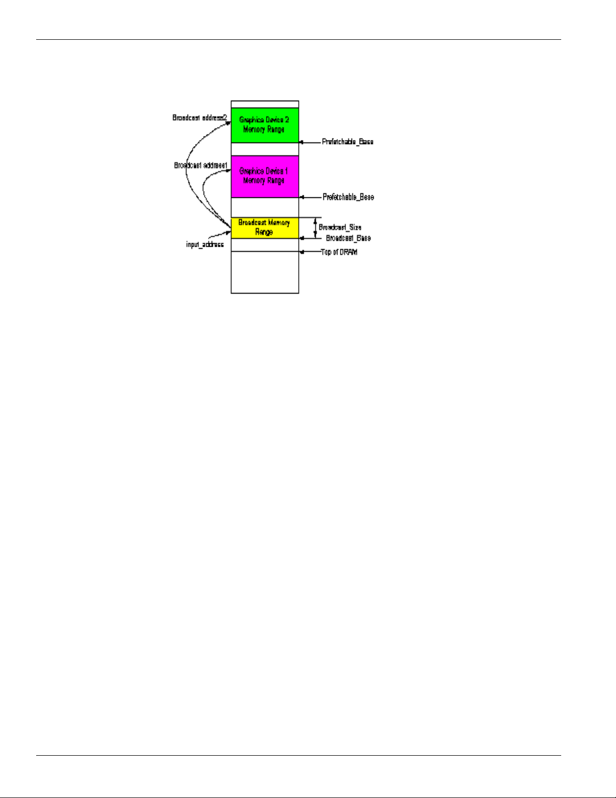
Figure 2-1 describes the algorithm for address translation and broadcast:
Figure 2-1 Address Translation And Broadcast
The Address Translation and Broadcast Algorithm is as follows:
• Broadcast_Address = input_address[63:0] – {BROADCAST_BASE[63:20], 20’b0} +
{Bridge_Prefetchable_BASE[63:20], 20’h} + {32’h0, BROADCAST_OFFSET[31:12], 12’h0}.
• Input_address refers the request address IOC received from CPU.
• BROADCAST_BASE refers to the broadcast memory range start address.
• Bridge_Prefetchable_BASE refers to external graphics device memory range start address.
• BROADCAST_OFFSET is the offset between translated broadcast base address and bridge Prefetchable_BASE
address.
Two broadcast addresses are obtained by applying two Bridge_Prefetchable_BASE addresses from the two PCI
configuration space. Therefore, a single CPU memory write request could be translated and redirected to two external
graphics devices by IOC. Note that this address translation and broadcast algorithm is only applicable to CPU memory
write requests. For CPU memory read requests, the address translation to the primary graphics device is performed using
the above equation, and the request is only forwarded to the primary graphics devices since only one response is expected
by the CPU.
• The 32-bit registers are defined as follows:
• [63:20] GPU_FB_BROADCAST_BASE // 1M aligned broadcast address
• [31:12] GPU_FB_BROADCAST_OFFSET // 4K aligned broadcast offset address
• [11:11] GPU_FB_BROADCAST_EN // Enable broadcast feature
• [10:10] GPU_FB_BROADCAST_PRIMARY // Primary GPU
• 0 = Lower device/port#
• 1 = Higher device/port#
• [07:00] GPU_FB_BROADCAST_SIZE // Size (8MB)
• If enabled, and the address is in range (address -> address + size), then the broadcast memory writes to both ports.
• Broadcast only works for applicable memory writes, and applicable reads will be sent to the primary device only.
• Broadcast is enabled when the enable bit is set, when both device 2 and device 3 bridges are enabled, and when the
memory space is enabled.
• The broadcast memory range should not conflict with any existing P2P memory range, or any BAR memory range.
• Broadcast address = input_address[63:0] - {GPU_FB_BROADCASE_BASE[63:20], 20'h0} +
{bridge_prefetchable_bar[63:20], 20'h0}
• + { 32'h0, GPU_FB_BROADCAST_OFFSET[31:12], 12'h0}
• Address [63:34] does not need to be checked since they are not used (the RS780 supports up to 16G memory space)
© 2009 Advanced Micro Devices, Inc. AMD 780G Register Programming Requirements 1.01
2-5
Page 16

Enabling/Disabling Peer-To-Peer Traffic Access
2.7 Enabling/Disabling Peer-To-Peer Traffic Access
The P2P master could be any device from the southbridge, devices connected behind P2P bridge 2, 3, 4, 5, 6, 7,9 and 10.
The P2P targets could be devices connected behind P2P bridge 1, 2, 3, 4, 5, 6, 7,9, 10. The southbridge cannot be a target
for trusted-PC purposes. The P2P traffic could be only memory writes. After bootup, by default all P2P traffic listed
above should be enabled. In order to disable a P2P target at a specific device, the following register bits in Table 2-5 need
to be set as follows:
Table 2-5 Enabling/Disabling Peer-To-Peer Traffic Settings
Devices Bit Settings
Bus0 Device1 nbmisc0x4C[2]
Bus0 Device2 nbmisc0x51[3]
Bus0 Device3 nbmisc0x53[3]
Bus0 Device4 nbmisc0x55[3]
Bus0 Device5 nbmisc0x57[3]
Bus0 Device6 nbmisc0x59[3]
Bus0 Device7 nbmisc0x5B[3]
Bus0 Device9 nbmisc0x5D[3]
Bus0 Device10 nbmisc0x5F[3]
2.8 Enabling/Disabling MVPU
MVPU is a feature that enables P2P traffic between external graphics devices (the devices behind P2P bridge 2 and 3) and
the internal graphics device (the device behind P2P bridge 1). The corresponding P2P traffic access enable bits are
described in section Table 2-5 above.
2.9 IOC Dynamic Clock Setup
The following clocks are in IOC:
• LCLK (free running)
• LCLK_MST (master branch)
• LCLK_SLV (slave branch - Note: This dynamic branch should not be used)
Note: Only LCLK_MST (master branch) and LCLK_SLV (slave branch) can be dynamically turned on and off.
The two bits that control IOC dynamic clocks are as follows:
• clkcfg0x8C[13] CLKGATE_DIS_IOC_LCLK_MST
• clkcfg0x8C[14] CLKGATE_DIS_IOC_LCLK_SLV (Note: Ensure that this bit is programmed to 1 in order to avoid
system instability)
Note: Clkconfig:0x94[27] CLKGATE_IOC_SLV_GFX - BIOS should program to 1 to disable clock gating on this
branch.
For both of these bits:
• 1=Dynamic clock is disabled
• 0=Dynamic clock is enabled
AMD 780G Register Programming Requirements 1.01 © 2009 Advanced Micro Devices, Inc.
2-6
Page 17
2.10 Interrupt Mapping
Table 2-6 Interrupt Mapping Settings
1 (internal graphics) INTA -> INTC, INTB->INTD
2.11 GSM Enable
Set nbmisind0x0C[13]=1 to enable GSM in the RS780.
Interrupt Mapping
Devices Bit Settings
2INTA -> INTC
3INTA -> INTD
4 INTA -> INTA
5 INTA -> INTB
6INTA -> INTC
7INTA -> INTD
9 INTA -> INTB
10 INTA -> INTC
© 2009 Advanced Micro Devices, Inc. AMD 780G Register Programming Requirements 1.01
2-7
Page 18

GSM Enable
This page intentionally left blank.
AMD 780G Register Programming Requirements 1.01 © 2009 Advanced Micro Devices, Inc.
2-8
Page 19

3.1 SBIOS Memory Clock Initialization
3.1.1 UMA Mode
RS780 boots up in synchronous UMA clock mode. The memory clock and HT clock are driven by the same HT PLL. In
UMA sync mode the memory PLL is not used and should be powered down.
• Program <NBMCIND:0x6> Bit[31] MC_MPLL_CONTROL.MPLL_POWERDOWN = ‘1’ to power down memory
PLL in sync mode.
3.1.2 Side-Port Async Mode
•
Step 1: Program IO 1XCLK skew delay by setting
• <NBMCIND:0x6> Bit[10:8] MC_MPLL_CONTROL.MPLL_SKEW1=0x1
• Step 2: Program current control for SCL for PLL to 0%
• < NBMCIND:0x8 > Bit[20:18] MC_MPLL_CONTROL3.MPLL_SCLBIAS = 0x1
• Step 3: Select memory PLL reference clock. Default is 100MHz HT reference and it should be used in normal
operation.
• <NBMCIND : 0x8> Bit[10] MC_MPLL_CONTROL3.MPLL_REFCLK_SEL (‘0’=100 MHz HT reference
clock; ‘1’=PCIE reference clock)
• Step 4: Program memory PLL settings for different operating frequencies.
• Feedback divider : < NBMCIND:0x7 > Bit[8:0] MC_MPLL_CONTROL2.MPLL_FBDIV
• Reference divider : < NBMCIND:0x7 > Bit[13:9] MC_MPLL_CONTROL2.MPLL_REFDIV
• Post divider (postdiv) : < NBMCIND:0x7 > Bit[15:14] MC_MPLL_CONTROL2.MPLL_POSTDIV
• Charge pump : < NBMCIND:0x7 > Bit[19:16] MC_MPLL_CONTROL2.MPLL_CP
• VCO mode : < NBMCIND:0x7 > Bit[21:20] MC_MPLL_CONTROL2.MPLL_VCO_MODE
• Loop filter mode: < NBMCIND:0x7 > Bit[31:28] MC_MPLL_CONTROL2.MPLL_LF_MODE
Chapter 3
Clock Settings
• Consider the following equation to calculate MCLK:
• P1 = 100MHz / (MPLL_REFDIV + 1)
• P2 = (MPLL_FBDIV[2:0] + 1) * (MPLL_FBDIV[8:3] + 1) * 2
• P3 = 2 * (MPLL_POSTDIV+1)
• MCLK = P1 * P2 / P3
• The divider settings should use the frequency plan in Table 3-1 from memory PLL specification.
• 200MHz settings:
• <NBMCIND:0x7> MC_MPLL_CONTROL2=0x00004018;
• 266MHz settings:
• <NBMCIND:0x7> MC_MPLL_CONTRO2=0x00114478;
• 333MHz settings:
• <NBMCIND:0x7> MC_MPLL_CONTROL2=0x00224498;
• 400MHz settings:
• <NBMCIND:0x7> MC_MPLL_CONTROL2=0x00000018;
• 533MHz settings:
• <NBMCIND:0x7> MC_MPLL_CONTROL2=0x00110478;
© 2009 Advanced Micro Devices, Inc. AMD 780G Register Programming Requirements 1.01
3-1
Page 20

SBIOS Memory Clock Initialization
• 667MHz settings:
• <NBMCIND:0x7> MC_MPLL_CONTROL2=0x00220498
• Note: For other frequencies, refer to TABLE X below.
• Step 5: Program PM mode PLL setting the same as nominal mode setting
• 200MHz:
• <NBMCIND:0xB> MC_MPLL_DIV_CONTROL=0x00004018
• <NBMCIND:0x9> Bit[11:8] MC_MPLL_FREQ_CONTROL.PM_MPLL_CP=0x0
• <NBMCIND:0x9> Bit[13:12] MC_MPLL_FREQ_CONTROL.PM_MPLL_VCO_MODE=0x0
• <NBMCIND:0x9> Bit[19:16] MC_MPLL_FREQ_CONTROL.PM_MPLL_LF_MODE=0x6
• 266MHz:
• <NBMCIND:0xB> MC_MPLL_DIV_CONTROL=0x00004478
• <NBMCIND:0x9> Bit[11:8] MC_MPLL_FREQ_CONTROL.PM_MPLL_CP=0x1
• <NBMCIND:0x9> Bit[13:12] MC_MPLL_FREQ_CONTROL.PM_MPLL_VCO_MODE=0x1
• <NBMCIND:0x9> Bit[19:16] MC_MPLL_FREQ_CONTROL.PM_MPLL_LF_MODE=0x4
• 333MHz:
• <NBMCIND:0xB> MC_MPLL_DIV_CONTROL=0x00004498
• <NBMCIND:0x9> Bit[11:8] MC_MPLL_FREQ_CONTROL.PM_MPLL_CP=0x2
• <NBMCIND:0x9> Bit[13:12] MC_MPLL_FREQ_CONTROL.PM_MPLL_VCO_MODE=0x2
• <NBMCIND:0x9> Bit[19:16] MC_MPLL_FREQ_CONTROL.PM_MPLL_LF_MODE=0x4
• 400MHz:
• <NBMCIND:0xB> MC_MPLL_DIV_CONTROL=0x00000018
• <NBMCIND:0x9> Bit[11:8] MC_MPLL_FREQ_CONTROL.PM_MPLL_CP=0x0
• <NBMCIND:0x9> Bit[13:12] MC_MPLL_FREQ_CONTROL.PM_MPLL_VCO_MODE=0x0
• <NBMCIND:0x9> Bit[19:16] MC_MPLL_FREQ_CONTROL.PM_MPLL_LF_MODE=0x6
• 533MHz:
• <NBMCIND:0xB> MC_MPLL_DIV_CONTROL=0x00000478
• <NBMCIND:0x9> Bit[11:8] MC_MPLL_FREQ_CONTROL.PM_MPLL_CP=0x1
• <NBMCIND:0x9> Bit[13:12] MC_MPLL_FREQ_CONTROL.PM_MPLL_VCO_MODE=0x1
• <NBMCIND:0x9> Bit[19:16] MC_MPLL_FREQ_CONTROL.PM_MPLL_LF_MODE=0x4
• 667MHz:
• <NBMCIND:0xB> MC_MPLL_DIV_CONTROL=0x00000498
• <NBMCIND:0x9> Bit[11:8] MC_MPLL_FREQ_CONTROL.PM_MPLL_CP=0x2
• <NBMCIND:0x9> Bit[13:12] MC_MPLL_FREQ_CONTROL.PM_MPLL_VCO_MODE=0x2
• <NBMCIND:0x9> Bit[19:16] MC_MPLL_FREQ_CONTROL.PM_MPLL_LF_MODE=0x4
• Note: For other PM frequencies, refer to Table 3-1 below.
• Step 6: Program memory PLL and DLL lock time
• Min. 10us calibration setup time: Calibration setup time = 10ns x <NBMCIND:0xA> Bit[11:8]
MC_MPLL_SEQ_CONTRL.MPLL_CAL_S_TIME x 512
• Min. 50ns calibration hold time: Calibration hold time = 10ns x <NBMCIND:0xA> Bit[15:12]
MC_MPLL_SEQ_CONTROL.MPLL_CAL_H_TIME x 4
• Min. 50us PLL lock time: MPLL lock time = 10ns x <NBMCIND:0xA> Bit[23:16]
MC_MPLL_SEQ_CONTROL.MPLL_LOCK_TIME x 256
• Min. 50us DLL lock time: MDLL lock time = 10ns x <NBMCIND:0xA> Bit[31:24]
MC_MPLL_SEQ_CONTROL.MDLL_LOCK_TIME x 256
AMD 780G Register Programming Requirements 1.01 © 2009 Advanced Micro Devices, Inc.
3-2
Page 21

• Step 7: Recalibrate the memory PLL
• Set < NBMCIND:0x6 > Bit[0] MC_MPLL_CONTROL.MPLL_CAL_TRIGGER = ’1’;
• Step 8: Wait for 200us;
• Step 9: Poll PLL lock signal < NBMCIND:0x6 > Bit[1] MC_MPLL_CONTROL.MPLL_LOCKED = ’1’;
• Step 10: Set < NBMCIND:0x6 > Bit[0] MC_MPLL_CONTROL.MPLL_CAL_TRIGGER = ’0’
• Step 11: Program <NBMCIND:0x2> Bit[20] MC_GENERAL_PURPOSE_2.MCLK_SRC_USE_MPLL = ‘0’ to
select asynchronous clock mode.
• Step 12: Start the memory initialization sequence.
3.2 Memory Clock Changes For POWERPLAY
Note: PowerPlay MCLK switching only applies to asynchronous clock mode for memory side port
• Step 1: Program MPLL divider in PM mode by setting
• < NBMCIND:0xB > Bit[8:0] MC_MPLL_DIV_CONTROL.PM_MPLL_FBDIV
• < NBMCIND:0xB > Bit[13:9] MC_MPLL_DIV_CONTROL.PM_MPLL_REFDIV
• < NBMCIND:0xB > Bit[15:14] MC_MPLL_DIV_CONTROL.PM_MPLL_POSTDIV
• Consider the following Equation to calculate MCLK in PM mode:
• P1 = 100MHz / (PM_MPLL_REFDIV + 1)
• P2 = (PM_MPLL_FBDIV[2:0] + 1) * (PM_MPLL_FBDIV[8:3] + 1) * 2
• P3 = 2 * (PM_MPLL_POSTDIV+1)
• MCLK = P1 * P2 / P3
• Use the settings in Table 3-1 to get the divider settings for the required frequencies. For example:
• 133MHz in PM mode
• MC_MPLL_DIV_CONTROL.PM_MPLL_FBDIV = 0x78
• MC_MPLL_DIV_CONTROL.PM_MPLL_REFDIV = 0x2
• MC_MPLL_DIV_CONTROL.PM_MPLL_POSTDIVS = 0x3
• Step 2: If MCLK < HT_CLK in PM mode, set < NBMCIND:0x9 > Bit[29]
MC_MPLL_FREQ_CONTROL.PM_MPLL_SLOWMCLK = 0x1 else 0x0
Memory Clock Changes For POWERPLAY
• Step 3: Program < NBMCIND:0x9 > Bit[0] MC_MPLL_FREQ_CONTROL.MPLL_PM_EN = 0x1
• Step 4: Program MPLL parameters in PM mode by setting the following:
• <NBMCIND:0x9> Bit[11:8] MC_MPLL_FREQ_CONTROL.PM_MPLL_CP
• <NBMCIND:0x9> Bit[13:12] MC_MPLL_FREQ_CONTROL.PM_MPLL_VCO_MODE
• <NBMCIND:0x9> Bit[19:16] MC_MPLL_FREQ_CONTROL.PM_MPLL_LF_MODE
• Use the settings in Table 3-1 to program the required frequencies. For example:
• MPLL parameter for 133MHz in PM mode
• MC_MPLL_FREQ_CONTROL.PM_MPLL_CP = 0x1
• MC_MPLL_FREQ_CONTROL.PM_VCO_MODE = 0x1
• MC_MPLL_FREQ_CONTROL.PM_LF_MODE = 0x4
• Step 5: Program the memory controller settings in different PM mode speed
• Refer to the AMD RS780 BIOS Developer’s Guide for more information.
• Step 6: Switch to PM mode MCLK by setting < NBMCIND:0x9 > Bit[1]
MC_MPLL_FREQ_CONTROL.MPLL_FREQ_SEL = 0x1
• Step 7: Poll for < NBMCIND:0x9 > Bit[6] MC_MPLL_FREQ_CONTROL.PM_SWITCHMCLK_BUSY = 0x0
© 2009 Advanced Micro Devices, Inc. AMD 780G Register Programming Requirements 1.01
3-3
Page 22

Switching Back From PM Mode to Nominal Mode
3.3 Switching Back From PM Mode to Nominal Mode
• Step 1: Set < NBMCIND:0x9 > Bit[1] MC_MPLL_FREQ_CONTROL.MPLL_FREQ_SEL = 0
• Step 2: Poll for < NBMCIND:0x9 > Bit[6] MC_MPLL_FREQ_CONTROL.PM_SWITCHMCLK_BUSY = 0x0.
Table 3-1 Memory PLL Settings For Supposed Frequencies
Target
(MHz)
100 100 0 1 1 4 4 0000 0110 00 800
133.3333 133.3333 0 3 1 16 4 0001 0100 01 1066.6667
166.6666 166.6666 0 1 1 5 3 0000 0110 01 1000
200 200 0 1 1 4 2 0000 0110 00 800
233.3333 233.3333 0 1 1 7 3 0000 0100 10 1400
266.6666 266.6666 0 3 1 16 2 0001 0100 01 1066.6667
300 300 0 1 1 6 2 0000 0100 01 1200
333.3333 333.3333 0 3 1 20 2 0010 0100 10 1333.3333
366.6666 366.6666 0 3 1 11 1 0001 0100 00 733.33333
400 400 0 1 1 4 1 0000 0110 00 800
433.3333 433.3333 0 3 1 13 1 0001 0100 00 866.66667
466.6666 466.6666 0 3 1 14 1 0001 0100 00 933.33333
500 500 0 1 1 5 1 0000 0110 01 1000
533.3333 533.3333 0 3 1 16 1 0001 0100 01 1066.6667
566.6666 566.6666 0 3 1 17 1 0001 0100 01 1133.3333
600 600 0 1 1 6 1 0000 0100 01 1200
633.3333 633.3333 0 3 1 19 1 0010 0100 10 1266.6667
666.6666 666.6666 0 3 1 20 1 0010 0100 10 1333.3333
100 100 0 1 1 4 4 0000 0110 00 800
112 112.5 0.5 2 1 9 4 0000 0100 00 900
124 123.8095 0.2 7 1 26 3 0010 1000 00 742.85714
136 136.1111 0.1 9 1 49 4 0011 1100 01 1088.8889
148 148.1481 0.15 9 1 40 3 0011 1000 00 888.88889
160 160 0 5 1 24 3 0010 0100 01 960
172 171.875 0.1 8 1 55 4 0011 1100 10 1375
184 184.375 0.4 8 1 59 4 0011 1100 10 1475
196 195.8333 0.15 8 1 47 3 0011 1100 01 1175
208 208.3333 0.35 4 1 25 3 0010 0100 01 1250
220 220 0 5 1 33 3 0010 1000 10 1320
232 231.25 0.75 8 1 37 2 0011 1000 00 925
244 243.75 0.25 8 1 39 2 0011 1000 01 975
256 256.25 0.25 8 1 41 2 0011 1100 01 1025
268 268.75 0.75 8 1 43 2 0011 1100 01 1075
280 280 0 5 1 28 2 0010 1000 01 1120
292 291.6666 0.35 6 1 35 2 0010 1000 01 1166.6667
304 305.5555 1.55 9 1 55 2 0011 1100 01 1222.2222
316 316.6666 0.65 3 1 19 2 0010 0100 10 1266.6667
328 327.7777 0.2 9 1 59 2 0011 1100 10 1311.1111
340 340 0 5 1 34 2 0010 1000 10 1360
352 350 2 1 1 7 2 0000 0100 10 1400
364 364.2857 0.3 7 1 51 2 0011 1100 10 1457.1429
376 375 1 4 1 15 1 0001 0100 00 750
388 387.5 0.5 8 1 31 1 0010 1000 00 775
400 400 0 1 1 4 1 0000 0110 00 800
412 412.5 0.5 8 1 33 1 0010 1000 00 825
Achieved
(MHz)
Error
(MHz)
Ref_div
3-bit
CMOS FB
div
6-bit
CMOS FB
div
POST
IICP
[3:0]
ILF_MOD
E[3 :0]
IVCO_MO
DE[1:0]
VCO freq
(MHz)
AMD 780G Register Programming Requirements 1.01 © 2009 Advanced Micro Devices, Inc.
3-4
Page 23
Power Saving Settings
Target
(MHz)
424 425 1 4 1 17 1 0001 0100 00 850
436 437.5 1.5 8 1 35 1 0010 1000 00 875
448 450 2 2 1 9 1 0000 0100 00 900
460 460 0 5 1 23 1 0010 0100 00 920
472 471.4285 0.55 7 1 33 1 0010 1000 01 942.85714
484 483.3333 0.65 6 1 29 1 0010 1000 01 966.66667
496 500 4 1 1 5 1 0000 0110 01 1000
508 511.1111 3.1 9 1 46 1 0011 1100 01 1022.2222
520 520 0 5 1 26 1 0010 1000 01 1040
532 533.3333 1.35 3 1 16 1 0001 0100 01 1066.6667
544 544.4444 0.45 9 1 49 1 0011 1100 01 1088.8889
556 555.5555 0.45 9 1 50 1 0011 1100 01 1111.1111
568 566.6666 1.35 3 1 17 1 0001 0100 01 1133.3333
580 580 0 5 1 29 1 0010 1000 01 1160
592 588.8888 3.1 9 1 53 1 0011 1100 01 1177.7778
604 600 4 1 1 6 1 0000 0100 01 1200
616 616.6666 0.65 6 1 37 1 0011 1000 01 1233.3333
628 628.5714 0.55 7 1 44 1 0011 1100 10 1257.1429
640 640 0 5 1 32 1 0010 1000 10 1280
652 650 2 2 1 13 1 0001 0100 10 1300
664 662.5 1.5 8 1 53 1 0011 1100 10 1325
676 675 1 4 1 27 1 0010 1000 10 1350
Achieved
(MHz)
Error
(MHz)
Ref_div
3-bit
CMOS FB
div
6-bit
CMOS FB
div
POST
IICP
[3:0]
ILF_MOD
E[3 :0]
IVCO_MO
DE[1:0]
VCO freq
(MHz)
3.4 Power Saving Settings
3.4.1 Enabling Dynamic Clocks
Table 3-2 Dynamic Clocks Settings
ASIC Rev Settings Function/Comment
CFG_CT_CLKGATE_HTIU <clkcfg:0xf8> = 0xcf30
CLKCFG.CLKGATE_DISABLE[31], [28], [26], [24] = 0x0
All Revs
3.4.2 Powering Down Efuse and Strap Block Clocks After Boot-Up
Table 3-3 Powering Down Efuse and Strap Block Clocks Settings
ASIC Rev Settings Function/Comment
All Revs
CLKCFG.CLKGATE_DISABLE2[26:24] = 0x0
CLKCFG.CLKGATE_DISABLE2[14] = 0x1
CLKCFG.CLK_TOP_SPARE_C[31:28]=0xe [27:26]=0x3
NBMCIND.MC_MCLK_CONTROL = 0xf000000
Intgfx mode: <CLKCFG: 0xCC> Bit[24:23] = 0x3;
<GpuF0MMReg:0x3080> Bit[8]
CG.CG_INTGFX_MISC.CG_CT_NB_EFUSE_CLK_DISABLE= 0x1
NB only mode: <CLKCFG: 0xCC> Bit[24:23] = 0x3
Enables North Bridge dynamic clocks to htiu and
mc
Powerdown efuse and strap block clocks in
integrated graphics mode
Powerdown efuse and strap block clocks in
northbridge only mode
© 2009 Advanced Micro Devices, Inc. AMD 780G Register Programming Requirements 1.01
3-5
Page 24
Power Saving Settings
3.4.3 Powering Down Graphics Core and Memory Clocks in Northbridge-Only Mode
Table 3-4 Powering Down Graphics core and Memory Clocks in NB-Only Mode Settings
ASIC Rev Settings Function/Comment
All Revs
<CLKCFG:0x8C> Bit[21] = 0x1
<CLKCFG:00xE4> Bit[0] = 0x1
Powers down reference clock to graphics core PLL in
northbridge only mode
Powers down clock to memory controller in
northbridge only mode
3.4.4 Powering Down IOC GFX Clock in No External Graphics Mode
Table 3-5 Powering Down IOC GFX Clock In No External Graphics Mode Settings
ASIC Rev Settings Function/Comment
All Revs
<CLKCFG:0xE8> Bit[17] = 0x1 Powers down clock to IOC GFX block in no external
graphics mode
3.4.5 PWM Controller
There are five PWM controllers mapped to five GPIO pins that can be used for voltage adjustment purpose after boot-up.
Table 3-6 PWM Controller/GPIO Pins Mapping
ASIC Rev Register setting Function/Comment
All Revs
1.CLK_TOP_PWM1_CTRL<CLKCFG:0xB0>
2. CLK_TOP_PWM2_CTRL<CLKCFG:0xB4>
3. CLK_TOP_PWM3_CTRL <CLKCFG:0xCC>
4. CLK_TOP_PWM4_CTRL<CLKCFG:0x4C>
5. CLK_TOP_PWM5_CTRL<CLKCFG:0x50>
1. PWM control on LVDS_BLON GPIO pin
2. PWM control on LVDS_ENA_BL GPIO pin
3. PWM control on STRP_DATA GPIO pin
4. PWM control on LVDS_DIGON GPIO pin
5. PWM control on TMDS_HPD GPIO pin
Each of the above PWM registers in PWM Controller/GPIO Pins Mapping has the following register fields:
• Bit[0]: Enable the PWM controller
• Bits[12:1]: Number of cycles in pulse period of a 100MHz reference clock
• Bits[24:13]: Number of high cycles in pulse period of a 100MHz reference clock
• Bit[25]: Output enable of the GPIO
The STRP_DATA pin by default is driving low, and register setting <clkcfg:0xE0> Bit[0] = ‘1’ is required before using
PWM or GPIO control.
The STRP_DATA pin is also used for core voltage scaling purposes. The CLK_TOP_PWM3_CTRL < CLKCFG:0xCC >
Bit[0] = ’0’ is required to enable the graphics device driver to have control on the STRP_DATA pin.
The register settings < nbmisind:0x40 > Bit[8] = ‘1’ and Bit[10] = ’1’ are required for using PWM1 on the LVDS_BLON
pin.
AMD 780G Register Programming Requirements 1.01 © 2009 Advanced Micro Devices, Inc.
3-6
Page 25

3.5 DOS Mode Power Saving
To disable the graphics engine clock branches when in DOS mode, program the following register in Table 3-7 during
boot.
Table 3-7 DOS Mode Power Saving Settings
ASIC Rev Settings Function/Comment
A12 1. CG_MISC_INPUT_3[9] = 0 <CLKCFG:0x90>
2. CG_INTGFX_MISC[31:20] = 0x9F3
3.6 HTPLL VCO Mode Setting
The HTPLL VCO mode setting should be configured in high-speed mode after boot-up.
• <clkcfg:0xD4> CLK_CFG_HTPLL_CNTL Bit[16:15] = “00”
• <clkcfg:0xD4> CLK_CFG_HTPLL_CNTL Bit[2:0] = “010”
• <clkcfg:0xE8> CLK_TOP_SPARE_C Bit[16] = “0”
DOS Mode Power Saving
Write 0x1
© 2009 Advanced Micro Devices, Inc. AMD 780G Register Programming Requirements 1.01
3-7
Page 26

HTPLL VCO Mode Setting
This page intentionally left blank.
AMD 780G Register Programming Requirements 1.01 © 2009 Advanced Micro Devices, Inc.
3-8
Page 27

4.1 Memory Initialization
For memory controller programming information, refer to the AMD RS780 BIOS Developer’s Guide.
Chapter 4
Memory Initialization
© 2009 Advanced Micro Devices, Inc. AMD 780G Register Programming Requirements 1.01
4-1
Page 28

Memory Initialization
This page intentionally left blank.
AMD 780G Register Programming Requirements 1.01 © 2009 Advanced Micro Devices, Inc.
4-2
Page 29

5.1 Introduction
This chapter describes the initialization and feature programming of the northbridge PCI Express subsystem. The
northbridge implements PCI Express point-to-point links to external devices.
There are 9 configurable PCI Express ports, which can be divided into 3 groups (implemented in hardware as 3 separate
cores):
• PCIE-GFX: 2 ports, 16 lanes in total. Each port is configurable from x1 to x8 link. The 2 ports can also be combined
to provide 1 x16 port (default configuration).
• PCIE-GPPSB: 1 SB port and 4 GPP ports, 8 lanes in total. The SB port provides a dedicated x4 link to the
southbridge. The remaining 4 lanes are distributed across the 4 GPP ports to support 4 different configurations: a)
4:0:0:0:0, b) 4:4:0:0:0, c) 4:2:2:0:0, d) 4:2:1:1:0 and e) 4:1:1:1:1 (default configuration).
• PCIE-GPP: 2 ports, 2 lanes in total. Each port provides a x1 link. The 2 ports can also be combined to provide a x2
link.
5.2 PCI Express Configuration Space
The PCI Express configuration space consists of the following four groups:
• PCIE Port Configuration Space (section 5.2.1)
• PCIE Core Index Space (section 5.2.2)
Chapter 5
PCIE Initialization
• PCIE Port Index Space (section 5.2.3)
• PCIE Extended Configuration Space (section 5.2.4)
5.2.1 PCIE Port Configuration Space
Each PCIE port has a standard Type 1 Virtual PCI-to-PCI bridge header in the PCI configuration space. These are devices
2 through 10 on PCI bus 0.
• GFX Port A: Device 2 (GFX0)
• GFX Port B: Device 3 (GFX1)
• GPPSB Port A: Device 8 (SB link, hidden by default)
• GPPSB Port B: Device 4 (GPP0)
• GPPSB Port C: Device 5 (GPP1)
• GPPSB Port D: Device 6 (GPP2)
• GPPSB Port E: Device 7 (GPP3)
• GPP Port A: Device 9 (GPP4)
• GPP Port B: Device 10 (GPP5)
© 2009 Advanced Micro Devices, Inc. AMD 780G Register Programming Requirements 1.01
5-1
Page 30

PCI Express Configuration Space
5.2.2 PCIE Core Index Space
The PCIE Core Index Space contains control and status registers that are generic to all PCIE ports in the northbridge.
This register space is accessed through an index/data register pair:
• NB_BIF_NB: NB_PCIE_INDX_ADDR: nbconfig: 0xe0
• NB_PCIE_INDX_ADDR: [7:0] - Address in PCIE Core
• GFX_GPPSB_SEL [18:16]:
• 000 – PCIE GFX Core
• 001 – PCIE GPPSB Core
• 010 – PCIE GPP Core
• 011 – Broadcast to all 3 cores
• All other values are unused
• NB_BIF_NB: NB_PCIE_INDX_DATA: nbconfig: 0xe4
Note: Registers in the core index space are referenced with the name PCIEIND or BIF_NB.
5.2.3 PCIE Port Index Space
The Port Index Space contains control and status registers that are specific to each port within the core. Each PCIE device
implements its own set of registers in this space.
Each PCIE device contains an index/data pair in its Virtual Bridge PCI configuration space to access the Port Index Space
registers. Please note the following information for the index/data register pair:
• Index register: bus 0, device X, register 0xE0.
• Data register: bus 0, device X, register 0xE4.
Note: Register descriptions are referenced with the name PCIEIND_P or BIF_NBP.
5.2.4 PCIE Extended Configuration Space
PCI Express extends the PCI configuration space from 256 bytes to 4096 bytes. Extended PCIE configuration space
memory maps 4KB for each device. The first 256 bytes of each 4KB are the same as PCI 2.3 configuration registers, and
the remaining 3840 bytes are PCIE specific configuration registers.
The northbridge uses NBCFG:NB_BAR3_PCIEXP_MMCFG nbconfig:0x1C (BAR3) to map the PCI Express Extended
Configuration Space to a 256MB range within the first 4GB of addressable memory. PCIE devices are accessed by
reading/writing to a memory mapped address that is based on the base address in BAR3. The PCIE target address is
formed as follows:
• Addr[11:2] = RegNum (Addr[11:8] is extended register field)
• Addr[14:12] = FunNum
• Addr[19:15] = DevNum
• Addr[20 + n-1:20] = BusNum
• Addr[33:20 + n] = Reserved for BAR3 match
AMD 780G Register Programming Requirements 1.01 © 2009 Advanced Micro Devices, Inc.
5-2
Page 31

PCI Express Configuration Space
Note: ‘n’ indicates how many bits are allocated for the bus number. This value is decided by BAR3BusRange in
NBCFG:NB_PCI_ARB[18:16] nbconfig:0x84 register. These relations are listed in Table 5-1 below:
Table 5-1 NBCFG:NB_PCI_ARB[18:16] nbconfig:0x84 register
ASIC Rev NBCFG:NB_PCI_ARB[18:16]· nbconfig:0x84 ‘n’
RS780 All Revs 3’b001 1
3’b010 2
3’b011 3
3’b100 4
3’b101 5
3’b110 6
3’b111 7
3’b000 8
Table 5-2 contains the programming procedure to enable BAR3:
Table 5-2 Enabling BAR3
ASIC
Rev
RS780 All
Revs
Step Register Settings Function/Comment
1 NBCFG:NB_IOC_CFG_CNTL[30]=1’b1 nbconfig:0x7c
NB_BAR3_PCIEXP_REG_WREN
Set bit [30] to 1
2 NBCFG:NB_PCI_ARB[18:16] nbconfig:0x84
BAR3BusRange
Enables BAR3 Register Access.
Programs BAR3 bus range.
Program bits [18:16]
3 NBCFG:NB_BAR3_PCIEXP_MMCFG[31:21] nbconfig:0x1c
MEM_BASE_HIGH
NBCFG:NB_BAR3_UPPER_PCIEXP_MMCFG[1:0]
nbconfig:0x20
MEM_BASE_UPPER
4 HTIUNBCFG:NB_HTIU_CFG[28]=1’b1 HTIUNBIND:0x32
NB_BAR3_PCIEXP_ENABLE
Set bit [28] to 1
Programs the BAR3 register.
Enables BAR3 decoding.
Note: The BAR3 memory upper address register is nbcfg0x20 (above 4G). The RS780 could support memory up to 16G,
so this register has to be set properly.
© 2009 Advanced Micro Devices, Inc. AMD 780G Register Programming Requirements 1.01
5-3
Page 32

Power-On and Reset State
5.3 Power-On and Reset State
After a Power-On or Reset event the North Bridge puts all of its PCI Express devices into their default states, which are
shown in Table 5-3 below:
Table 5-3 Power-On and Reset State
ASIC Rev PCI Device Number (PCIE Port) Link Training Number of Lanes Supported
RS780 All Revs Dev 2 (PCIE-GFX Port A) Disabled 1, 2, 4, 8, or 16
Dev 3 (PCIE-GFX Port B) Disabled 1, 2, 4, or 8
Dev 4 (PCIE-GPPSB Port B) Disabled 1, 2, or 4
Dev 5 (PCIE-GPPSB Port C) Disabled 1
Dev 6 (PCIE-GPPSB Port D or - C in 4:2:x:x:0 mode) Disabled 1 or 2
Dev 7 (PCIE-GPPSB Port E or - D in 4:2:1:1:0 mode) Disabled 1
Dev 8 (PCIE-GPPSB Port A) Enabled 1 or 2 or 4
Dev 9 (PCIE-GPP Port A) Disabled 1
Dev 10 (PCIE-GPP Port B) Disabled 1
Note: PCI device 8 (Dev 8) does not appear in the PCI configuration space by default.
5.4 PCIE GFX Configurations
The x16 PCIE GFX interface is fully multiplexed to provide as many directly connected display options as possible. Each
output format can be mapped to any of the four-lane groups (0-3, 4-7, 8-11 and 12-15) in the 16 available lanes.
However, there are only 3 separate PLLs associated with lanes 0-3 (PLL A), 4-7 (PLL B) and 8-15 (PLL C). The
supported configurations in RS780 are detailed below.
5.4.1 PCIE Modes Only
The PCIE GFX core can support up to 2 PCIE devices. Each PCIE device can be a GFX or a GPP device. Table 5-4
outlines all the supported PCIE configurations.
Table 5-4 PCIE Configurations
Lanes 0 to 3 4 to 7 8 to 11 12 to 15
1
2
3
4
5
6
7
8
9
10
11
12
13
14
15
16
17
GFX x16 A
GFX x8 A
GFX x8 A
GFX x8 A GFX x8 B
GPP x4 A
GPP x4 B
GPP x4 A
GPP x4 B
GPP x4 A GPP x4 B
GPP x4 A GPP x4 B
GPP x4 A GPP x4 B
GPP x4 B GPP x4 A
GPP x4 A GPP x4 B
GFX x8 A GPP x4 B
GFX x8 A GPP x4 B
GPP x4 B GFX x8 A
GPP x4 A GFX x8 B
The core should be configured to run in single port mode if only Port A is present and in dual port mode whenever Port B
is present (regardless of Port A). The GFX ports are held from link training by default. To enable a GFX port, the
corresponding HOLD_TRAINING bit must be set to 0 to allow link training to proceed.
The SBIOS is responsible for programming the lane and clock muxing specific to each case. Refer to Chapter 7: PCIE
Initialization for DDI for programming details.
Note: This programming must be done before hold training is released.
AMD 780G Register Programming Requirements 1.01 © 2009 Advanced Micro Devices, Inc.
5-4
Page 33

5.4.1.1 Single Port Configuration (Default)
• PCIE_LINK_CFG – NBMISCIND:0x8
• Set MULTIPORT_CONFIG_GFX (Bits[11:8]) = 4’b0000
Table 5-5 Single Port Configuration (Default)
Device Possible Link Width HOLD_TRAINING Bit
Dev 2 1, 2, 4, 8 or 16 PCIE_LINK_CFG[4]
5.4.1.2 Dual Port Configuration
• PCIE_LINK_CFG – NBMISCIND:0x8
• Set MULTIPORT_CONFIG_GFX (Bits[11:8]) = 4’b0101
Table 5-6 Dual Port Configuration
Device Possible Link Width HOLD_TRAINING Bit
Dev 2 1, 2, 4 or 8 PCIE_LINK_CFG[4]
Dev 3 1, 2, 4 or 8 PCIE_LINK_CFG[5]
Table 5-7 Dual Port Configuration Register Settings
ASIC Rev Step Register Settings Function/Comment
RS780 All Revs 1 PCIE_NBCFG_REG6 – NBMISCIND:0x36
STRAP_BIF_all_valid (active low)
PCIE GFX Configurations
De-asserts STRAP_BIF_all_valid for PCIE-GFX
core.
5.4.2 DDI Modes Only
In the RS780, DDI is a collective term used to describe the supported display formats, which include DVI, HDMI and
DisplayPort. DVI and HDMI can run in either single link (x4, DDI_SL) or dual link (x8, DDL_DL) mode. DisplayPort
can run in x1, x2 or x4 mode.
Due to the fact that lanes 8-15 are sharing PLL C, the subgroups of lanes 8-11 and lanes 12-15 cannot be used
simultaneously to support 2 independent display outputs. All the supported configurations are detailed in Table 5-8 below.
Table 5-8 DDI Configurations
Lanes 0 to 3 4 to 7 8 to 11 12 to 15
1
2
3
4
5
6
7
8
9
10
11
Set bit [31] to 1
2 PCIE_LINK_CFG - NBMISCIND:0x8
MULTIPORT_CONFIG_GFX
Set bits[11:8] to 4’b0101
3 PCIE_NBCFG_REG6 – NBMISCIND:0x36
STRAP_BIF_all_valid (active low)
Set bit [31] to 0
DDI_SL
DDI_SL
DDI_SL DDI_SL
DDI_DL
DDI_SL DDI_SL
DDI_SL DDI_SL
DDI_SL DDI_SL
DDI_SL DDI_SL
Enables dual port configuration
Asserts STRAP_BIF_all_valid for PCIE-GFX
core.
DDI_SL
DDI_SL
DDI_DL
The VBIOS/Driver will be responsible for DDI programming sequence. In the case of DDI modes only, the SBIOS can
pass control over to the VBIOS/Driver after powering down any unused lanes and PLLs.
© 2009 Advanced Micro Devices, Inc. AMD 780G Register Programming Requirements 1.01
5-5
Page 34

PCIE GPPSB Configurations
5.4.3 PCIE and DDI Combined Modes
PCIE and DDI modes can also be combined to use simultaneously, the supported configurations are listed in the following
chart. For each group of 8 lanes (lanes 0-7 and lanes 8-15), only 1 DDI or 1 PCIE device can be used at any one time.
Table 5-9 PCIE and DDI Configurations
Lanes 0 to 3 4 to 7 8 to 11 12 to 15
1
2
3
4
5
6
7
8
9
10
11
12
13
14
DDI_SL GFX x8 A
DDI_SL DDI_SL GFX x8 A
GPP x4 A GPP x4 B DDI_SL
GPP x4 A GPP x4 B DDI_SL
GPP x4 A GPP x4 B DDI_DL
DDI_SL GPP x4 A GPP x4 B
DDI_SL DDI_SL GPP x4 A GPP x4 B
GFX x8 A DDI_SL
GFX x8 A DDI_SL
GFX x8 A DDI_DL
DDI_SL GFX x8 A
DDI_DL GFX x8 A
DDI_SL GPP x4 A GPP x4 B
DDI_DL GPP x4 A GPP x4 B
The SBIOS is responsible for PCIE mode programming (same as section 5.4.1) and the VBIOS/Driver is responsible for
completing the DDI programming.
5.5 PCIE GPPSB Configurations
The SB link shares the same PCIE core with 4 other GPP devices. The SB port has 4 dedicated lanes and the 4 GPP ports
share among 4 lanes, for a total of 8 lanes. The following configurations are supported:
• Default Configuration E (4:1:1:1:1), STRAP_BIF_LINK_CONFIG_GPPSB = 4’b0100 (section 5.5.2)
• Configuration A (4:0:0:0:0), STRAP_BIF_LINK_CONFIG_GPPSB = 4’b0000 (section 5.5.3)
• Configuration B (4:4:0:0:0), STRAP_BIF_LINK_CONFIG_GPPSB = 4’b0001 (section 5.5.4)
• Configuration C (4:2:2:0:0), STRAP_BIF_LINK_CONFIG_GPPSB = 4’b0010 (section 5.5.5)
• Configuration D (4:2:1:1:0), STRAP_BIF_LINK_CONFIG_GPPSB = 4’b0011 (section 5.5.6)
Note: STRAP_BIF_LINK_CONFIG_GPPSB = StrapsOutputMux_7 – NBMISCIND:0x67, bits [7:4]
AMD 780G Register Programming Requirements 1.01 © 2009 Advanced Micro Devices, Inc.
5-6
Page 35

5.5.1 Device Remapping
The device remapping feature provides the ability to map a PCIE slot to any device number. There are 2 possible ways of
remapping:
• Manual Remapping
The slot-to-device number mapping is specified through the register setting in Table 5-10:
Table 5-10 Device Remapping
NB_PROG_DEVMAP_EN, bit [0] 0=Device mapping disabled (default)
GPP_PORTB_DEVMAP, bits [7:4] 0=Map to Device 4
GPP_PORTC_DEVMAP, bits [11:8] 0=Map to Device 4
GPP_PORTD_DEVMAP, bits [15:12] 0=Map to Device 4
GPP_PORTE_DEVMAP, bits [19:16] 0=Map to Device 4
PCIE GPPSB Configurations
NBCFG: NB_PROG_DEVICE_REMAP_0 NBMISCIND:0x20
1=Device remapping enabled using GPP_PORT*_DEVMAP
1=Map to Device 5
2=Map to Device 6
3=Map to Device 7
1=Map to Device 5
2=Map to Device 6
3=Map to Device 7
1=Map to Device 5
2=Map to Device 6
3=Map to Device 7
1=Map to Device 5
2=Map to Device 6
3=Map to Device 7
• Automatic Remapping
The remapping is done automatically according to the PCIE GPPSB configuration so that the slot to device number
mapping is always the same. The SBIOS should program the field in Table 5-11 to enable this feature by default.
Table 5-11 Automatic Remapping
NBCFG: NB_PROG_DEVICE_REMAP_0 NBMISCIND:0x20
IOC_PCIE_Dev_Remap_Dis, bit [1] 0=Automatic device remapping enabled
1=Automatic device remapping disabled
5.5.2 Default Configuration E (STRAP_BIF_LINK_CONFIG_GPPSB = 4’b0100)
The default configuration only has the SB port enabled. The GPP ports are held from link training. To enable the GPP
ports, the corresponding HOLD_TRAINING bit must be set to 0 to allow link training to proceed.
• PCIE_LINK_CFG – NBMISCIND:0x8
Table 5-12 Default Configuration E
Device Associated Lanes HOLD_TRAINING Bit
Dev 8 (Port A) SB_RX/TX0
SB_RX/TX1
SB_RX/TX2
SB_RX/TX3
Dev 4 (Port B) GPP_RX/TX0 PCIE_LINK_CFG[21]
Dev 5 (Port C) GPP_RX/TX1 PCIE_LINK_CFG[22]
Dev 6 (Port D) GPP_RX/TX2 PCIE_LINK_CFG[23]
Dev 7 (Port E) GPP_RX/TX3 PCIE_LINK_CFG[24]
PCIE_LINK_CFG[20]
© 2009 Advanced Micro Devices, Inc. AMD 780G Register Programming Requirements 1.01
5-7
Page 36

PCIE GPPSB Configurations
5.5.3 Configuration A (STRAP_BIF_LINK_CONFIG_GPPSB = 4’b0000)
This configuration only supports the SB port and no GPP ports.
Table 5-13 Configuration A
Device Associated Lanes HOLD_TRAINING Bit
Dev 8 (Port A) SB_RX/TX0
SB_RX/TX1
SB_RX/TX2
SB_RX/TX3
5.5.4 Configuration B (STRAP_BIF_LINK_CONFIG_GPPSB = 4’b0001)
This configuration is primarily used to support high performance GPP devices. Both the SB and the GPP links will have
4-lanes.
Table 5-14 Configuration B
Device Associated Lanes HOLD_TRAINING Bit
Dev 8 (Port A) SB_RX/TX0
SB_RX/TX1
SB_RX/TX2
SB_RX/TX3
Dev 4 (Port B) GPP_RX/TX0
GPP_RX/TX1
GPP_RX/TX2
GPP_RX/TX3
PCIE_LINK_CFG[20]
PCIE_LINK_CFG[21]
PCIE_LINK_CFG[20]
5.5.5 Configuration C (STRAP_BIF_LINK_CONFIG_GPPSB = 4’b0010)
In addition to the 4-lane SB, this configuration supports two x2 GPP devices.
Table 5-15 Configuration C
Device Associated Lanes HOLD_TRAINING Bit
Dev 8 (Port A) SB_RX/TX0
SB_RX/TX1
SB_RX/TX2
SB_RX/TX3
Dev 4 (Port B) GPP_RX/TX0
GPP_RX/TX1
Dev 6 (Port C) GPP_RX/TX2
GPP_RX/TX3
PCIE_LINK_CFG[20]
PCIE_LINK_CFG[21]
PCIE_LINK_CFG[22]
5.5.6 Configuration D (STRAP_BIF_LINK_CONFIG_GPPSB = 4’b0011)
This configuration provides a x4 SB, one x2 GPP and two x1 GPP ports.
Table 5-16 Configuration D
Device Associated Lanes HOLD_TRAINING Bit
Dev 8 (Port A) SB_RX/TX0
SB_RX/TX1
SB_RX/TX2
SB_RX/TX3
Dev 4 (Port B) GPP_RX/TX0
GPP_RX/TX1
Dev 6 (Port C) GPP_RX/TX2 PCIE_LINK_CFG[22]
Dev 7 (Port D) GPP_RX/TX3 PCIE_LINK_CFG[23]
PCIE_LINK_CFG[20]
PCIE_LINK_CFG[21]
AMD 780G Register Programming Requirements 1.01 © 2009 Advanced Micro Devices, Inc.
5-8
Page 37

5.5.7 Switching GPPSB Configurations
Since the SB link must be alive for SBIOS code execution, a special programming sequence must be performed to switch
between configurations. This sequence will cause the hardware to assert reset to the GPPSB core, load the new
configuration and deassert reset for the link to re-train at the new configuration.
Table 5-17 Switching GPPSB Configurations
ASIC Rev Step Register Settings Function/Comment
RS780 All
Revs
1 PCIE_NBCFG_REG7 - NBMISCIND:0x37
reconfig_gppsb_en
Set bit[12] to 1
2 PCIE_NBCFG_REG7 - NBMISCIND:0x37
reconfig_gppsb_atomic_reset_dis
Set bit[15] to 1
3 PCIE_NBCFG_REG7 - NBMISCIND:0x37
reconfig_gppsb_link_config_xfer_mode
Set bit[17] to 1
4a StrapsOutputMux_7 - NBMISCIND:0x67
STRAP_BIF_LINK_CONFIG_GPPSB
Set bits[7:4] to desired configuration
4b StrapsOutputMux_6 – NBMISCIND:0x66
STRAP_BIF_all_valid (active low)
PCIE GPPSB Configurations
Enables GPPSB reconfiguration
Sets desired GPPSB configurations
De-asserts STRAP_BIF_all_valid for PCIE-GPPSB
core.
Set bit [31] to 1
5 PCIE_NBCFG_REG7 - NBMISCIND:0x37
reconfig_gppsb
Read bit[14]
6 PCIE_NBCFG_REG7 - NBMISCIND:0x37
reconfig_gppsb
Write the inversion of bit[14] read back from step 5
7 StrapsOutputMux_6 – NBMISCIND:0x66
STRAP_BIF_all_valid (active low)
Set bit [31] to 0
8 Wait for 1ms
9 PCIE_LC_STATE0 – PCIEIND_P: 0xA5 in Dev 8
LC_CURRENT_STATE
Poll for bits[5:0] = 5’h10
10 PCIE_LC_STATE0 – PCIEIND_P: 0x12A in Dev 8
VC_NEGOTIATION_PENDING
Poll for bit[1] = 0
Asserts STRAP_BIF_all_valid for PCIE-GPPSB core.
Waits until SB has trained to L0
Ensures that virtual channel negotiation is completed.
© 2009 Advanced Micro Devices, Inc. AMD 780G Register Programming Requirements 1.01
5-9
Page 38

PCIE GPP Configurations
5.6 PCIE GPP Configurations
The GPP core only has 2 available lanes, supporting either two x1 GPP devices or one x2 GPP device. The GPP ports are
held from link training. To enable the GPP ports, the corresponding HOLD_TRAINING bit must be set to 0 to allow link
training to proceed.
5.6.1 Default Configuration D
•
PCIE_NBCFG_REG15 – NBMISCIND: 0x2d
• Set LINK_CONFIG (Bits[10:7]) = 4’b0011
Table 5-18 Default Configuration D
Device Associated Lanes HOLD_TRAINING Bit
Dev 9 GPP_RX/TX4 PCIE_NBCFG_REG15[4]
Dev 10 GPP_RX/TX5 PCIE_NBCFG_REG15[5]
5.6.2 Configuration C
•
PCIE_NBCFG_REG15 – NBMISCIND: 0x2d
• Set LINK_CONFIG (Bits[10:7]) = 4’b0010
Table 5-19 Configuration C
Device Associated Lanes HOLD_TRAINING Bit
Dev 9 GPP_RX/TX4
PCIE_NBCFG_REG15[4]
GPP_RX/TX5
Table 5-20 Configuration C Register Settings
ASIC Rev Step Register Settings Function/Comment
RS780 All Revs 1 PCIE_NBCFG_REGA – NBMISCIND:0x22
STRAP_BIF_all_valid (active low)
Set bit [14] to 1
2 PCIE_NBCFG_REG15 – NBMISCIND:0x2d
LINK_CONFIG
Set bits[10:7] to 4’b0010
3 PCIE_NBCFG_REG6 – NBMISCIND:0x22
STRAP_BIF_all_valid (active low)
Set bit [14] to 0
De-asserts STRAP_BIF_all_valid for PCIE-GPP
core.
Sets configuration to C
Asserts STRAP_BIF_all_valid for PCIE-GPP core.
AMD 780G Register Programming Requirements 1.01 © 2009 Advanced Micro Devices, Inc.
5-10
Page 39

5.7 PCIE Link Training Sequence
The link training sequence cannot be interrupted and no other BIOS code can be added in between.
Note: The contents of Table 5-21 continues onto the next two pages of this document.
Table 5-21 PCIE Link Training Sequence
ASIC Rev Step Register Setting Function/Comment
RS780 All
Revs
1 Release hold training for Device * by clearing the
corresponding HOLD_TRAINING bit to 0.
2 Delay 200us
3 BIF_NBP:PCIE_LC_STATE0 ·PCIEIND_P:0xA5
Read back the following values:
LC_CURRENT_STATE = [5:0]
LC_PREV_STATE1 = [13:8]
LC_PREV_STATE2 = [21:16]
LC_PREV_STATE3 = [29:24]
If any read back value is 6’h3F -> then perform
CF9 reset;
If LC_CURRENT_STATE = 6’h00 to 6’h04, then
no device is present. Keep checking for up to
40ms, if no device is present Æ Go to Step 8.
Otherwise, go to Step 4.
PCIE Link Training Sequence
The HOLD_TRAINING bit can be found in section 5.4 (GFX),
section 5.5 (GPPSB), and section 5.6 (GPP).
Detects if there is any card present from reading back
PCIE_LC_STATE0 in Port Index space of Device*.
© 2009 Advanced Micro Devices, Inc. AMD 780G Register Programming Requirements 1.01
5-11
Page 40

PCIE Link Training Sequence
RS780 All
Revs
4 BIF_NBP:PCIE_LC_STATE0 ·PCIEIND_P:0xA5
LC_CURRENT_STATE
Read back bits [5:0].
If LC_CURRENT_STATE = 6’h06 -> read back
current link width by reading bits [6:4] of the
following register:
BIF_NBP:PCIE_LC_LINK_WIDTH_CNTL[6:4]
PCIEIND_P:0xA2
LC_LINK_WIDTH_RD
If [6:4]=3’h4 and lane reversal is not enable set:
BIF_NB:PCIE_P_PAD_FORCE_DIS[7:4]=4’hf·
PCIEIND:0x65
BIF_NB:PCIE_P_PAD_FORCE_DIS[15:12]=4’hf·
PCIEIND:0x65
If [6:4]=3’h4 and lane reversal is enabled set:
BIF_NB:PCIE_P_PAD_FORCE_DIS[3:0]=4’hf·
PCIEIND:0x65
BIF_NB:PCIE_P_PAD_FORCE_D[11:8]=4’hf·
PCIEIND:0x65
If [6:4]=3’h3 and lane reversal is not enabled set:
BIF_NB:PCIE_P_PAD_FORCE_DIS[7:2]=4’hf·
PCIEIND:0x65
BIF_NB:PCIE_P_PAD_FORCE_DIS[15:10]=4’hf·
PCIEIND:0x65
If [6:4]=3’h3 and lane reversal is enabled set:
BIF_NB:PCIE_P_PAD_FORCE_DIS[5:0]=4’hf·
PCIEIND:0x65
BIF_NB:PCIE_P_PAD_FORCE_D[13:8]=4’hf·
PCIEIND:0x65
CMOS option (disabled by default).
This programming sequence is required if some lanes on the end
point are broken. It is specific for GFX card in single slot
configuration.
If [6:4]=3’h2 and lane reversal is not enabled set:
BIF_NB:PCIE_P_PAD_FORCE_DIS[7:1]=4’hf·
PCIEIND:0x65
BIF_NB:PCIE_P_PAD_FORCE_DIS[15:9]=4’hf·
PCIEIND:0x65
If [6:4]=3’h2 and lane reversal is enabled set:
BIF_NB:PCIE_P_PAD_FORCE_DIS[6:0]=4’hf·
PCIEIND:0x65
BIF_NB:PCIE_P_PAD_FORCE_D[14:8]=4’hf·
PCIEIND:0x65
Toggle GPIO reset to the PCIe slot.
Got to Step5.
If [6:4] takes any other values than described
above; go to Step 5.
5 BIF_NBP:PCIE_LC_STATE0 ·PCIEIND_P:0xA5
LC_CURRENT_STATE
Read back bits [5:0].
If LC_CURRENT_STATE = 6’h07 -> Device is in
compliance state (training sequence is done).
Move to train the next device;
If LC_CURRENT_STATE = 6’h10 -> go to step 6
Otherwise, keep polling for up to 2 seconds, then
perform CF9 reset. This should only be repeated
for a maximum of 15 times.
Detects if link is in Compliance State or it is trained to L0 from
reading back PCIE_LC_STATE0 [5:0] in Device*.
If LC_CURRENT_STATE can not reach 6’h10 or
6’h07 -> go to Step 9.
AMD 780G Register Programming Requirements 1.01 © 2009 Advanced Micro Devices, Inc.
5-12
Page 41

Overall PCIE Programming Sequence
RS780 All
Revs
6 BIF_NBP:PCIE_VC0_RESOURCE_STATUS[1]·
pcieConfigDev*:0x12a
VC_NEGOTIATION_PENDING
Read bit[1]
Read back value 0 means link negotiation is
successful -> go to Step 8
Read back value 1 means the link needs to be
re-trained -> go to Step 7
7 Set bit[8] = 1 and set bits[2:0] to be equal to
bits[6:4] of the following register:
BIF_NBP:PCIE_LC_LINK_WIDTH_CNTL
PCIEIND_P:0xA2
LC_RECONFIG_NOW, bit[8]
LC_LINK_WIDTH, bit[2:0] <LC_LINK_WIDTH_RD, bit[6:4]
Wait for 5ms after the bits above are set, then go
back to Step 2 (stay in this loop indefinitely).
8 For AMD GFX Cards only -> go to section
5.12.9.1
After the implementation of RV370/RV380
Initialization Workaround, and after reading back
the Device ID for the non-AMD Device, as well as
AMD devices for which this workaround is not
applicable, perform the following:
BIF_NB:PCIE_CI_CNTL[9]=1’b0PCIEIND:0x20
CI_RC_ORDERING_DIS
Clear bit[9] to 0.
9 Hide the bridge for non-hot-plug device;
Set the hold training bit to 1 (see Step 1);
Power down the port, then move to the train the
next device.
Detects if Data Link Negotiation is performed, by reading bit [1] of
BIF_NBP:PCIE_VC0_RESOURCE_STATUS[1]· pcieConfigDev*:
0x12a
Retrains the link.
RV370/RV380 Initialization Workaround.
When no device is detected or the link cannot be trained properly,
than these 3 steps should be performed.
5.8 Overall PCIE Programming Sequence
The overall PCIE programming sequence can be divided into the following parts:
• PCIE-GFX Core Initialization (section 5.9)
• PCIE-GPPSB and PCIE-GPP Cores Initialization (5.10)
• Dynamic Link Width Control (5.11)
• PCI Enumeration and Special Features Programming Sequence (5.12)
Note: Section 5.9 and section 5.10 should be implemented as separate threads in the SBIOS so that they can be executed
in parallel.
© 2009 Advanced Micro Devices, Inc. AMD 780G Register Programming Requirements 1.01
5-13
Page 42

PCIE-GFX Core Initialization
5.9 PCIE-GFX Core Initialization
The initialization sequence should be executed in the same order as the sections are organized.
5.9.1 REFCLK Options
•
External Clock Mode (Default Mode): an external clock chip is used to drive a dedicated GFX REFCLK
Note: For ASIC Rev A11 ONLY - When accessing PCIE_NBCFG_REG10 (NBMISCIND:0x28), the write enable
bit must be set for both reads and writes.
Table 5-22 External Clock Mode
ASIC Rev Step Register Settings Function/Comment
RS780 All
Revs
1 PCIE_NBCFG_REG8 – NBMISCIND:0x38
B_PCLK_BIDIR_TX_EN
Set bit[29] to 0
2 PCIE_NBCFG_REG8 – NBMISCIND:0x38
B_PCLK_BIDIR_RX_EN
Set bit[28] to 1
Disables the GFX REFCLK transmitter so that the GFX
REFCLK PAD can be driven by an external source.
Enables GFX REFCLK receiver to receive the REFCLK
from an external source.
3 PCIE_NBCFG_REG10 – NBMISCIND:0x28
B_PREFCLK_SEL_A
Set bits[7:6] to 2’b01
4 PCIE_NBCFG_REG10 – NBMISCIND:0x28
B_PREFCLK_SEL_B
Set bits[9:8] to 2’b01
5 PCIE_NBCFG_REG10 – NBMISCIND:0x28
B_PREFCLK_SEL_C
Set bits[11:10] to 2’b01
6 StrapsOutputMux_C – NBMISCIND:0x6C
REFCLK_BIDIR_SEL
Set bit[31] to 1
Selects the GFX REFCLK to be the source for PLL A.
Selects the GFX REFCLK to be the source for PLL B.
Selects the GFX REFCLK to be the source for PLL C.
All 3 PLLs will be configured to have the same source in
SBIOS. The PLLs may have different sources in DDI
modes and the setting will be overwritten by the
VBIOS/Driver.
Selects the single ended GFX REFCLK to be the
source for core logic.
• Internal Clock Mode: SB REFCLK is routed internally to be the source of GFX REFCLK
Table 5-23 Internal Clock Mode
ASIC Rev Step Register Settings Function/Comment
RS780 All
Revs
1 PCIE_NBCFG_REG8 – NBMISCIND:0x38
B_PCLK_BIDIR_TX_EN
Set bit[29] to 1
2 PCIE_NBCFG_REG8 – NBMISCIND:0x38
B_PCLK_BIDIR_RX_EN
Enables the GFX REFCLK transmitter so that the
GFX REFCLK PAD can be driven by the SB REFCLK.
Disables GFX REFCLK receiver from receiving the
REFCLK from an external source.
Set bit[28] to 0
3 PCIE_NBCFG_REG10 – NBMISCIND:0x28
B_PREFCLK_SEL_A
Set bits[7:6] to 2’b00
4 PCIE_NBCFG_REG10 – NBMISCIND:0x28
B_PREFCLK_SEL_B
Set bits[9:8] to 2’b00
Selects SB REFCLK to be the source for PLL A.
Selects SB REFCLK to be the source for PLL B.
AMD 780G Register Programming Requirements 1.01 © 2009 Advanced Micro Devices, Inc.
5-14
Page 43

ASIC Rev Step Register Settings Function/Comment
5 PCIE_NBCFG_REG10 – NBMISCIND:0x28
B_PREFCLK_SEL_C
Set bits[11:10] to 2’b00
6 StrapsOutputMux_C – NBMISCIND:0x6C
REFCLK_BIDIR_SEL
Set bit[31] to 0
5.9.2 Lane Reversal (CMOS Option - Disabled by Default)
There should be 2 CMOS options for Port A and Port B:
• PCIE-GFX Port A Lane Reversal (Single/Dual Configuration)
• PCIE-GFX Port B Lane Reversal (Dual Configuration)
Table 5-24 Lane Reversal (CMOS Option - Disabled by Default)
ASIC
Rev
RS780
All Revs
Step Register Settings Function/Comment
1 PCIE_NBCFG_REG6 – NBMISCIND:0x36
STRAP_BIF_all_valid (active low)
PCIE-GFX Core Initialization
Selects SB REFCLK to be the source for PLL C.
All 3 PLLs will be configured to have the same source
in SBIOS. The PLLs may have different sources in
DDI modes and the setting will be overwritten by the
VBIOS/Driver.
Selects the single ended SB REFCLK to be the
source for core logic.
De-asserts STRAP_BIF_all_valid for
PCIE-GFX core.
2 PCIE_NBCFG_REG3 - NBMISCIND:0x33
3 PCIE_NBCFG_REG3 - NBMISCIND:0x33
4 PCIE_NBCFG_REG6 – NBMISCIND:0x36
5.9.3 GFX Overclocking
Table 5-25 GFX Overclocking
ASIC Rev Step Register Settings Function/Comment
RS780 All
Revs
1 Program the external clock chip to a different
2 PCIE_NBCFG_REG6 – NBMISCIND:0x36
Set bit [31] to 1
STRAP_BIF_REVERSE_LANES_GFX_A
Set bit[2] to 1
STRAP_BIF_REVERSE_LANES_GFX_B
Set bit[3] to 1
STRAP_BIF_all_valid (active low)
Set bit [31] to 0
frequency
B_P90PLL_IBIAS
Set bits[13:4] to 10’hB5
Enables lane reversal for GFX Port A
Enables lane reversal for GFX Port B
Asserts STRAP_BIF_all_valid for
PCIE-GFX core.
Increases PLL BW for 6G operation.
© 2009 Advanced Micro Devices, Inc. AMD 780G Register Programming Requirements 1.01
5-15
Page 44

PCIE-GFX Core Initialization
5.9.4 Reset PCIE-GFX Core
Table 5-26 Reset PCIE-GFX Core
ASIC Rev Step Register Settings Function/Comment
RS780 All
Revs
1 PCIE_LINK_CFG – NBMISCIND:0x8
CALIB_RESET_GFX
GLOBAL_RESET_GFX
Set bits[15:14] to 2’b11
2 PCIE_LINK_CFG – NBMISCIND:0x8
CALIB_RESET_GFX
Set bit[14] to 0
3 Wait for at least 200us
4 PCIE_LINK_CFG – NBMISCIND:0x8
GLOBAL_RESET_GFX
Set bit[15] to 0
5.9.5 Reset PCIE-GFX Slot
Table 5-27 Reset PCIE-GFX Slot
ASIC Rev Step Register Settings Function/Comment
RS780 All
Revs
1 Desktop reference board: SLP_S2/GPM9#
Mobile reference board: INTH#/GPIO36
2 Use the Delay Training CMOS Option described in the
next section
Asserts both calibration reset and global reset
De-asserts calibration reset
De-asserts global reset
Program the GPIO in the SB700 to reset the PCIE-GFX
slot.
Program delay link training timer.
5.9.6 Delay Training Option (CMOS Option – Default 2ms)
Some PCIE devices may require additional initialization time after a reset is de-asserted before they can train the link
properly. A typical delay of 2ms is sufficient for most devices. In order to accommodate devices that require additional
delay, a CMOS option with a selectable time from 0 to 200 ms, with increments of 1ms, should be implemented. Training
to the slots should not be released until the timer expires.
5.9.7 Transmitter Drive Strength (CMOS Option – Default 22mA)
The transmitter driving strength can be adjusted to give better signal integrity for the PCIE lanes.
Table 5-28 Transmitter Driver Strength (CMOS Option - Default 22mA)
ASIC Rev Step Register Settings Function/Comment
RS780 All
Revs
1 PCIE_NBCFG_REG5 – NBMISCIND:0x35
B_P90TX_DRV_STR[1:0] for GFX
Set bits[3:2] according to CMOS option
Possible CMOS options:
2’b00: 18mA nominal
2’b01: 20mA nominal
2’b10: 22mA nominal
2’b11: 24mA nominal
AMD 780G Register Programming Requirements 1.01 © 2009 Advanced Micro Devices, Inc.
5-16
Page 45

5.9.8 Program PCIE Memory Mapped Configuration Space
Table 5-29 Program PCIE Memory Mapped Configuration Space
ASIC
Rev
RS780
All Revs
Step Register Settings Function/Comment
1 NB_IOC_CFG_CNTL – NBCONFIG:0x7C
NB_BAR3_PCIEXP_REG_WREN
Set bit[30] to 1
2 NB_PCI_ARB – NBCONFIG:0x84
BAR3BusRange
Set bits[18:16] to 3’b000
3 NB_BAR3_PCIEXP_MMCFG – NBCONFIG:0x1C
MEM_BASE_HIGH
Set bits[31:0] to 32’hE0000000
4 NB_BAR3_UPPER_PCIEXP_MMCFG – NBCONFIG:
0x20
MEM_BASE_UPPER
Set bits[1:0] to 2’b00
5 NB_IOC_CFG_CNTL – NBCONFIG:0x7C
NB_BAR3_PCIEXP_REG_WREN
PCIE-GFX Core Initialization
Enables writes to BAR3 register
See section 5.2.4 for details
Sets memory upper address to be above 4G
Disables BAR3 writes
Set bits[30] to 0
6 NB_HTIU_CFG – HTIUNBIND:0x32
NB_BAR3_PCIEXP_ENABLE
Set bits[28] to 1
Enables BAR3 decoding
5.9.9 GEN1 Software Compliance (CMOS Option – Disabled by Default)
There should be 2 CMOS options for Port A and Port B:
• PCIE-GFX Port A GEN1 Software Compliance (Single/Dual Configuration)
• PCIE-GFX Port B GEN1 Software Compliance (Dual Configuration)
Table 5-30 GEN1 Software Compliance (CMOS Option - Disabled by Default)
ASIC
Rev
RS780
All Revs
BIF_NBP:PCIEP_STRAP_LC -- PCIEIND_P:0xC0
STRAP_FORCE_COMPLIANCE
Set bit[13] to 1
Register Settings Function/Comment
Forces transmitter to output compliance pattern at Gen1
rate.
© 2009 Advanced Micro Devices, Inc. AMD 780G Register Programming Requirements 1.01
5-17
Page 46

PCIE-GFX Core Initialization
5.9.10 GEN2 Software Compliance (CMOS Option – Disabled by Default)
There should be 2 CMOS options for Port A and Port B:
• PCIE-GFX Port A GEN2 Software Compliance (Single/Dual Configuration)
• PCIE-GFX Port B GEN2 Software Compliance (Dual Configuration)
Table 5-31 GEN2 Software Compliance (CMOS Option - Disabled by Default)
ASIC Rev Step Register Settings Function/Comment
RS780 All
Revs
1 BIF_NBP:PCIE_LC_SPEED_CNTL -- PCIEIND_P:0xA4
LC_GEN2_EN_STRAP
Set bit[0] to 1
2 NBCFG: PCIE_NBCFG_REG4 – NBMISCIND: 0x34
STRAP_BIF_DE_EMPHASIS_SEL (port A)
Set bit[5] to 1
NBCFG: PCIE_NBCFG_REGA – NBMISCIND: 0x22
STRAP_BIF_DE_EMPHASIS_SEL (port B)
Set bit[6] to 1
3 BIF_NBP:LINK_CNTL2 -- pcieConfigDev*:0x88
TARGET_LINK_SPEED
Set bits[3:0] to 4’h2
4 BIF_NBP:LINK_CNTL2 -- pcieConfigDev*:0x88
ENTER_COMPLIANCE
Enables GEN2 capability of the device.
Advertises -3.5 dB de-emphasis value
in TS1 Data Rate Identifier
Advertise the link speed to be Gen2.
Forces transmitter to output compliance
pattern at Gen2 rate.
Set bit[4] to 1
5.9.11 De-Emphasis Strength -3.5dB/-6dB in GEN2 (CMOS Option - Disabled by Default)
Table 5-32 De-Emphasis Strength -3.5dB/-6dB in GEN2 Settings
ASIC Rev Step Register Settings Function/Comment
RS780 All
Revs
1 NBCFG: PCIE_NBCFG_REG4 – NBMISCIND: 0x34
STRAP_BIF_DE_EMPHASIS_SEL (port A)
Set bit[5] to 0
NBCFG: PCIE_NBCFG_REGA – NBMISCIND: 0x22
STRAP_BIF_DE_EMPHASIS_SEL (port B)
Set bit[6] to 0
Advertises -6 dB de-emphasis value in
TS1 Data Rate Identifier.
Default value is -3.5dB.
AMD 780G Register Programming Requirements 1.01 © 2009 Advanced Micro Devices, Inc.
5-18
Page 47

5.9.12 Core Initialization
Table 5-33 Core Initialization
ASIC Rev Step Register Settings Function/Comment
RS780 All
Revs
1 BIF_NBP:PCIE_RX_CNTL -- PCIEIND_P:0x70
2 BIF_NBP:PCIE_RX_CNTL -- PCIEIND_P:0x70
3 BIF_NB:PCIE_CI_CNTL -- PCIEIND:0x20
4 BIF_NB:PCIE_CNTL -- PCIEIND:0x10
5 BIF_NBP:PCIEP_PORT_CNTL -- PCIEIND_P :0x10
6 BIF_NB:PCIE_CI_CNTL -- PCIEIND:0x20
7 BIF_NB:PCIE_HW_DEBUG -- PCIEIND:0x2
RX_RCB_CPL_TIMEOUT
Set bits[18:16] to 3’h4
RX_RCB_CPL_TIMEOUT_MODE
Set bit[19] to 1
CI_SLV_ORDERING_DIS
Clear bit[8] to 0
RX_SB_ADJ_PAYLOAD_SIZE
Set bits[12:10] to 3’b100
SLV_PORT_REQ_EN
Clear bit[0] to 0
CI_RC_ORDERING_DIS
Set bit[9] to 1
HW_00_DEBUG (REGS_DLP_IGNORE_IN_L1_EN)
PCIE-GFX Core Initialization
Sets timeout to 100ms/4 = 25ms
RCB Cpl timeout on link down (to
shorten enumeration time).
Enable slave ordering logic.
Sets DMA payload size to 64 bytes.
Blocks DMA traffic during C3 state.
Disables RC ordering logic so that
Picard can return a dummy master
completion without receiving an ACK.
Ignores DLLPs during L1 so that txclk
can be turned off .
Set bit [0] to 1
8 BIF_NBP:PCIE_LC_TRAINING_CNTL -- PCIEIND_P:0xA1
LC_DONT_GO_TO_L0S_IF_L1_ARMED
Set bit [11] to 1
9 NBCFG:StrapsOutputMux_A -- NBMISCIND:0x6A
Set bit [17] to 1
10 BIF_NBP:PCIE_LC_CNTL2 -- PCIEIND_P:0xB1
LC_WAIT_FOR_LANES_IN_LW_NEG
Set bit [23] to 1
11 BIF_NBP:PCIE_LC_CNTL2 -- PCIEIND_P:0xB1
LC_DEASSERT_RX_EN_IN_L0s
Set bit[19] to 1
12 BIF_NBP:PCIE_LC_CNTL2 -- PCIEIND_P:0xB1
LC_ENABLE_RX_CR_EN_DEASSERTION
Set bit [28] to 1
13 NBCFG:PCIE_NBCFG_REG4 -- NBMISCIND:0x34
B_P90RX_INCAL_FORCE
Set bit[10] to 1
14 NBCFG:PCIE_NBCFG_REG4 -- NBMISCIND:0x34
B_P90RX_CLKG_EN
Prevents LC to go from L0 to
Rcv_L0s if L1 is armed.
CMGOOD_OVERRIDE for end point
initiated lane degradation.
Sets the timer in Config state from
20us to 1us for short and up/down
reconfiguration.
De-asserts RX_EN in L0s.
Enables de-assertion of
PG2RX_CR_EN to lock clock
recovery parameter when lane is in
electrical idle in L0s.
Turns off offset calibration.
Enables Rx Clock gating in CDR
Set bit[22] to 1
© 2009 Advanced Micro Devices, Inc. AMD 780G Register Programming Requirements 1.01
5-19
Page 48

PCIE-GFX Core Initialization
ASIC Rev Step Register Settings Function/Comment
15 BIF_NBP:PCIE_LC_CNTL -- PCIEIND_P:0xA0
16 BIF_NB:PCIE_P_CNTL -- PCIEIND:0x40
17 BIF_NBP:PCIE_LC_CNTL2 -- PCIEIND_P:0xB1
18 BIF_NBP:PCIE_LC_TRAINING_CNTL -- PCIEIND_P:0xA1
19 BIF_NB:PCIE_P_CNTL -- PCIEIND:0x40
20 BIF_NB:PCIE_STRAP_PI -- PCIEIND:0xC2
LC_16X_CLEAR_TX_PIPE
Set bits[7:4] to4’h3
P_ELEC_IDLE_MODE
Set bits [15:14] to 2’b10
LC_BLOCK_EL_IDLE_IN_L0
Set bit[20] to 1
LC_DONT_GO_TO_L0S_IF_L1_ARMED
Set bit [11] to 1.
RXP_REALIGN_ON_EACH_TSX_OR_SKP
Set bit[28] to 0
STRAP_LDSK_X1_BYPASS
Sets number of TX Clocks to drain TX
Pipe to 3.
Lets PI use Electrical Idle from PHY
when turning off PLL in L1 at Gen2
speed instead Inferred Electrical Idle.
NOTE: LC still uses Inferred Electrical
Idle.
Prevents the Electrical Idle from
causing a transition from Rcv_L0 to
Rcv_L0s.
Prevents the LTSSM from going to
Rcv_L0s if it has already
acknowledged a request to go to L1.
LDSK only taking deskew on
deskewing error detect
Bypasses lane de-skew logic if in x1
RS780 A13
and beyond
Set bit [14] to 1
21 NBCFG:PCIE_NBCFG_REG5 -- NBMISCIND:0x35
B_PG2PLL_IDLEDET_TH[1:0]
Set bits [22:21] to 2’b10
22 NBCFG: PCIE_NBCFG_REG4 – NBMISCIND: 0x34
STRAP_BIF_DE_EMPHASIS_SEL (port A)
Set bit[5] to 0
NBCFG: PCIE_NBCFG_REGA – NBMISCIND: 0x22
STRAP_BIF_DE_EMPHASIS_SEL (port B)
Set bit[6] to 0
23 BIF_NBP:PCIE_LC_SPEED_CNTL -- PCIEIND_P:0xA4
LC_GEN2_EN_STRAP
Set bit[0] to 0
24 BIF_NBP:PCIE_LC_LINK_WIDTH_CNTL[13]=1’b1·PCIEIND_P:0xA2
LC_UPCONFIGURE_DIS
Set bit[13] to 1
25 NBCFG: PCIE_NBCFG_REG9 – NBMISCIND: 0x39
STRAP_BIF_DSN_EN
Set bit[10] to 0
26 BIF_NBP:PCIE_STRAP_MISC2[0] – PCIEIND:0xC1
STRAP_LINK_BW_NOTIFICATION_CAP_EN
Set bit[0] to 1
27 PCIEP_HW_DEBUG - PCIEIND_P:0x02
HW_11_DEBUG
Set bit[11] to 1
Sets Electrical Idle Threshold
Advertises -6 dB de-emphasis value
in TS1 Data Rate Identifier
Only if CMOS Option in section 5.9.11
is enabled.
Disables GEN2 capability of the
device.
Disables advertising Upconfigure
Support.
This capacity is required since links
wider than x1 and/or multiple link
speed are supported
Enables NVG86 ECO.
Note: This is applicable to port A only.
AMD 780G Register Programming Requirements 1.01 © 2009 Advanced Micro Devices, Inc.
5-20
Page 49

PCIE-GFX Core Initialization
ASIC Rev Step Register Settings Function/Comment
RS780 All
Revs
RS780 All
Revs
RS780 All
Revs
RS780 All
Revs
RS780 All
Revs
28 BIF_NB:PCIE_STRAP_MISC2[2] - PCIEIND:0xC1
STRAP_MSTCPL_TIMEOUT_EN
Set bit[2] to 0
29 PCIE_NBCFG_REG6[28] - NBMISCIND:0x36
STRAP_BIF_DEEMPH_BIF_SEL_A
STRAP_BIF_DEEMPH_BIF_SEL_B
Set bit[28] to 1
30 BIF_NB:PCIE_CNTL2 -- PCIEIND:0x1C
TX_ARB_ROUND_ROBIN_EN set to 1
TX_ARB_SLV_LIMIT set to 4
TX_ARB_MST_LIMIT set to 4
31 PCIEP_HW_DEBUG - PCIEIND_P:0x02
HW_12_DEBUG
Set bit[12] to 1
32 PCIEP_HW_DEBUG - PCIEIND_P:0x02
HW_13_DEBUG
Set bit[13] to 1
33 PCIE_LC_TRAINING_CNTL – PCIEIND_P:0xA1
LC_RESET_ASPM_L1_NAK_TIMER
Hides and disables the completion
timeout method.
Use the bif_core de-emphasis
strength by default.
Set TX arbitration algorithm to round
robin.
Internal interrupt generation not
depending on INT_DIS bit.
Internal pme generation not
depending on Native PME bit set.
Workaround for Broadcom Network
Card bug.
Clear bit [26] to 0
34 PCIE_STRAP_PI - PCIEIND:0xC2
STRAP_PHY_RX_INCAL_FORCE
set bit[25] to 1
5.9.13 Autonomous GEN2 Speed Change (CMOS Option – Disabled by Default)
The following 2 options are available:
• PCIE-GFX Port A Autonomous GEN2 (Single/Dual Configuration)
• PCIE-GFX Port B Autonomous GEN2 (Dual Slot Configuration)
Table 5-34 Autonomous GEN2 Speed Change (CMOS Option - Disabled by Default)
ASIC Rev Step Register Settings Function/Comment
RS780 All
Revs
1 BIF_NBP:LINK_CNTL2 -- pcieCopcieConfigDev*:0x88
TARGET_LINK_SPEED
Set bits[3:0] to 4’h2
2 NBCFG: PCIE_NBCFG_REG4 – NBMISCIND: 0x34
STRAP_BIF_DE_EMPHASIS_SEL (port A)
Set bit[5] to 1
NBCFG: PCIE_NBCFG_REGA – NBMISCIND: 0x22
STRAP_BIF_DE_EMPHASIS_SEL (port B)
Set bit[6] to 1
3 BIF_NBP:PCIE_LC_SPEED_CNTL -- PCIEIND_P:0xA4
LC_GEN2_EN_STRAP
For all ports.
Work around for L1 efficiency
degradation due to PCIE eIDLE PHY
glitch
For all ports
Sets TARGET_LINK_SPEED to
GEN2.
Advertises -3.5 dB de-emphasis
value in TS1 Data Rate Identifier
Disables GEN2 capability of the
device.
Set bit[0] to 1
4 BIF_NBP:PCIEP_STRAP_LC -- PCIEIND_P:0xC0
STRAP_AUTO_RC_SPEED_NEGOTIATION_DIS
Set bit [15] to 0
Sets AUTO RC SPEED
NEGOTIATION
© 2009 Advanced Micro Devices, Inc. AMD 780G Register Programming Requirements 1.01
5-21
Page 50

PCIE-GFX Core Initialization
5 BIF_NBP:PCIE_LC_SPEED_CNTL -- PCIEIND_P:0xA4
6 BIF_NBP:PCIE_LC_LINK_WIDTH_CNTL[13]=1’b0·PCIEIND_P:0xA2
5.9.14 Link Training
Release hold training (by setting the corresponding hold training bit in the table below) and then start the link training
procedure outlined in Section 5.7 PCIE Link Training Sequence.
Table 5-35 Link Training
5.9.15 Power Down Control
In order to save power, inactive lanes and PLLs should be powered down.
5.9.15.1 Inactive Lanes
There are a total of 16 register bits assigned to control the powering down of inactive lanes. The transmitter and the
receiver of a lane can be powered down separately; in the case of an inactive lane, both the transmitter and the receiver
should be powered down.
Each register bit controls the powering down of 2 lanes; the corresponding register bit should be set to 1 when both lanes
are inactive. The register and lane mappings are specified as follows:
Enables Gen2 Speed Change on any
LC_MULT_UPSTREAM_AUTO_SPD_CHNG_EN
Set bit [29] to 1
LC_UPCONFIGURE_DIS
Clear bit[13] to 0.
Device HOLD_TRAINING Bit
Dev 2 PCIE_LINK_CFG[4]
Dev 3 PCIE_LINK_CFG[5]
surprised link down
Clears up gating off Upconfigure
Support.
• Transmitter: B_PTX_PDNB_FDIS = PCIE_P_PAD_FORCE_DIS – PCIEIND: 0x65, bits[7:0]
• Receiver: B_PRX_PDNB_FDIS = PCIE_P_PAD_FORCE_DIS – PCIEIND: 0x65, bits[15:8]
Table 5-36 Inactive Lanes
Inactive
Lanes
0-1 1 1
2-3 1 1
4-5 1 1
6-7 1 1
8-9 1 1
10-11 1 1
12-13 1 1
14-15 1 1
5.9.15.2 Inactive PLLs
There are 3 PLLs associated with lanes 0-3 (PLL A), 4-7 (PLL B) and 8-15 (PLL C). In order to achieve maximum power
saving, the transmitter and receiver output buffers of the PLL can also be powered down separately. There are 3 different
parameters to control each PLL:
• B_PPLL_PDNB_FDIS: Power down the PLL completely, no current consumption except for leakage.
• B_P90_PLL_BUF_PDNB_TX_FDIS: Power down the transmitter output buffers.
• B_P90_PLL_BUF_PDNB_RX_FDIS: Power down the receiver output buffers.
A PLL can be powered down completely (all 3 parameters set to 1) when all the lanes associated with it are inactive.
B_PRX_PDNB_FDIS B_PTX_PDNB_FDIS
15 14 13 12 11 10 9 8 7 6 5 4 3 2 1 0
The receiver of a PLL can be powered down when lanes associated with it are running in DDI mode due to the absence of
receiver data stream in DDI mode. (The receiver of a lane is also powered down in DDI mode, which is automatically
done by hardware).
AMD 780G Register Programming Requirements 1.01 © 2009 Advanced Micro Devices, Inc.
5-22
Page 51

The register control is specified as follows:
Note: For ASIC Rev A11 ONLY - When accessing PCIE_NBCFG_REG16 (NBMISCIND:0x2e), the write enable bit
must be set for both reads and writes.
• B_PPLL_PDNB_FDIS = PCIE_NBCFG_REG16 – NBMISCIND: 0x2e, bits[6:4]
• B_P90PLL_BUF_PDNB_TX_FDIS = PCIE_NBCFG_REG16 – NBMISCIND: 0x2e, bits[18:16]
• B_P90PLL_BUF_PDNB_RX_FDIS = PCIE_NBCFG_REG16 – NBMISCIND: 0x2e, bits[22:20]
Table 5-37 Inactive PLLs
Inactive
Lanes
0-3 1 1 1
4-7 1 1 1
8-15 1 1 1
B_P90PLL_BUF_PDNB_RX_FDIS B_P90PLL_BUF_PDNB_TX_FDIS B_PPLL_PDNB_FDIS
22 21 20 18 17 16 6 5 4
5.9.15.3 Powering Down in PCIE Only Modes
5.9.15.3.1 Finding the Inactive Lanes and PLLs
The following procedure can be used to find out which of the 16 lanes are active.
• Single Slot Configuration
Table 5-38 Single Slot Configuration Settings
ASIC
Rev
RS780 All
Revs
Step Register Settings Function/Comment
1 BIF_NB: PCIE_DEBUG_CNTL – PCIEIND: 0x12
DEBUG_PORT_EN
PCIE-GFX Core Initialization
Select Port A
Set bits[7:0] to 8’h1
2 BIF_NB: PCIE_LC_STATUS2 – PCIEIND: 0x29
LC_TOTAL_INACTIVE_LANES
Read back bits[15:0]
Each of the 16 bits of the read back value
represents a lane.
Bit [0] represents lane 0.
Bit [15] represents lane 15.
1=Inactive lane
0=Active lane
© 2009 Advanced Micro Devices, Inc. AMD 780G Register Programming Requirements 1.01
5-23
Page 52

PCIE-GFX Core Initialization
• Dual Slot Configuration
Table 5-39 Dual Slot Configuration Settings
ASIC
Rev
RS780 All
Revs
Step Register Settings Function/Comment
1 BIF_NB: PCIE_DEBUG_CNTL – PCIEIND: 0x12
2 BIF_NB: PCIE_LC_STATUS2 – PCIEIND: 0x29
3 BIF_NB: PCIE_DEBUG_CNTL – PCIEIND: 0x12
4 BIF_NB: PCIE_LC_STATUS2 – PCIEIND: 0x29
DEBUG_PORT_EN
Set bits[7:0] to 8’h1
LC_TOTAL_INACTIVE_LANES
Read back bits[7:0]
DEBUG_PORT_EN
Set bits[7:0] to 8’h2
LC_TOTAL_INACTIVE_LANES
Read back bits[7:0]
Select Port A
Each of the 8 bits of the read back value
represents a lane.
Bit [0] represents lane 0.
Bit [7] represents lane 7.
1=Inactive lane
0=Active lane
Select Port B
Each of the 8 bits of the read back value
represents a lane.
Bit [0] represents lane 8.
Bit [7] represents lane 15.
1=Inactive lane
0=Active lane
AMD 780G Register Programming Requirements 1.01 © 2009 Advanced Micro Devices, Inc.
5-24
Page 53

PCIE-GFX Core Initialization
Table 5-40 Inactive Lanes and PLLS
Lanes 0 to 3 4 to 7 8 to 11 12 to 15
GFX x16 A
GFX x8 A
GPP x4 A
GPP x4 B
GPP x4 A GPP x4 B
10
11
12
13
14
15
16
17
1
2
3
4
5
6
7
8
9
GPP x4 A
GPP x4 A GPP x4 B
GPP x4 A GPP x4 B
GPP x4 A GPP x4 B
GPP x4 A GFX x8 B
GFX x8 A
GFX x8 A GFX x8 B
GPP x4 B
GPP x4 B GPP x4 A
GFX x8 A GPP x4 B
GFX x8 A GPP x4 B
GPP x4 B GFX x8 A
Table 5-41 (for normal mode) and Table 5-42 (for reversal mode) specify the inactive lanes (0-15) and inactive PLLs (A,
B, C) in each of the supported configurations in Table 5-40 above. The register settings for the power down can then be
worked out based on the mapping in section 5.9.15.1 (“Inactive Lanes”) and in section 5.9.15.2 (“Inactive PLLs”).
Table 5-41 Normal Mode
Lanes
10-15
2 Same as case 1
3 0-15
4Port A:
5 Same as case 1 N/A
60-15
7 Same as case 3 N/A
80-15
9Port A:
10 Same as case 4 N/A
11 Same as case 15 N/A
12 Same as case 16 N/A
x0 x1, x2 x4 x8
A, B, C
A, B, C
0-7
A, B
Port B:
8-15
C
A, B, C
A, B, C
0-3, 8-11
A, C
Port B:
4-7, 12-15
B, C
No inactive PLL
Lane Reversal Disabled
2-15
B, C
0-7, 10-15
A, B
Port A:
2-7
B
Port B:
10-15
0-3, 6-7, 8-15
C
0-11, 14-15
A, B
Port A:
2-3, 8-11
C
Port B:
6-7, 12-15
C
4-15
B, C
0-7, 12-15
A, B
Port A:
4-7
B
Port B:
12-15
No inactive PLL
0-3, 8-15
C
0-11
A, B
Port A:
8-11
C
Port B:
12-15
C
8-15
C
0-7
A, B
Port A:
No inactive lane
No inactive PLL
Port B:
No inactive lane
No inactive PLL
N/A
N/A
N/A
N/A
N/A
© 2009 Advanced Micro Devices, Inc. AMD 780G Register Programming Requirements 1.01
5-25
Page 54

PCIE-GFX Core Initialization
13 Port A:
14 Same as case 4
15 Port A:
16 Port A:
17 Same as case 4
Table 5-42 Reversal Mode
Lanes
10-15
2 Same as case 1
3 Same as case 1
4Port A:
5 Same as case 1 N/A
6 Lane reversal is not supported in this configuration
7 Lane reversal is not supported in this configuration
8 Lane reversal is not supported in this configuration
9 Lane reversal is not supported in this configuration
10 Lane reversal is not supported in this configuration
11 Lane reversal is not supported in this configuration
12 Lane reversal is not supported in this configuration
13 Lane reversal is not supported in this configuration
14 Same as case 4
15 Lane reversal is not supported in this configuration
16 Lane reversal is not supported in this configuration
17 Same as case 4
Port A:
0-3, 8-11
A
Port B:
4-7, 12-15
B
C if A&B are x0
0-7
A, B
Port B:
8-15
C
8-15
C
Port B:
0-7
A, B
x0 x1, x2 x4 x8
A, B, C
0-7
A, B
Port B:
8-15
C
0-3, 10-11
A
Port B:
4-7, 14-15
B
Port A:
2-7
B
Port B:
8-11, 14-15
No inactive PLL
Port A:
10-15
No inactive PLL
Port B:
0-3, 6-7
A
Lane Reversal Enabled
0-13
A, B
Port A:
0-5
A
Port B:
8-13
No inactive PLL
Port A:
0-3
A
Port B:
4-7
B
Port A:
4-7
B
Port B:
8-11
No inactive PLL
Port A:
12-15
No inactive PLL
Port B:
0-3
A
0-11
A, B
Port A:
0-3
A
Port B:
8-11
No inactive PLL
N/A
Port A:
No inactive lane
No inactive PLL
Port B:
N/A
Port A:
No inactive lane
No inactive PLL
Port B:
N/A
0-7
A, B
Port A:
No inactive lane
No inactive PLL
Port B:
No inactive lane
No inactive PLL
5.9.15.3.2 Selecting TXCLK Source For Core Logic
The programming in this step must be executed before the register writes for the power down. The PCIE core logic
requires a TXCLK which comes from either PLL A or PLL C; therefore, the clock muxes must be programmed to select
the clock source from a running PLL.
• PLL A is to be powered down
AMD 780G Register Programming Requirements 1.01 © 2009 Advanced Micro Devices, Inc.
5-26
Page 55

PCIE-GFX Core Initialization
Table 5-43 Selecting TXCLK Source For Core Logic
ASIC Rev Step Register Settings Function/Comment
RS780 All
Revs
1 PCIE_PDNB_CNTL – NBMISCIND: 0x7
GFX_TXCLK_SEL
Set bit[16] to 1
2 PCIE_PDNB_CNTL – NBMISCIND: 0x7
GFX_TXCLK_SND_RCV_0_SEL
GFX_TXCLK_SND_RCV_1_SEL
GFX_TXCLK_SND_RCV_2_SEL
GFX_TXCLK_SND_RCV_3_SEL
Set bit[12] = 1
Set bit[13] = 1
Set bit[14] = 1
Set bit[15] = 1
3 PCIE_PDNB_CNTL – NBMISCIND: 0x7
IO_TXCLK_A_SEL
IO_TXCLK_B_SEL
IO_TXCLK_C_SEL
Set bits[21:20] = 2’b10
Set bits[23:22] = 2’b10
Set bits[25:24] = 2’b10
Selects PLL C to be the source clock
for TXCLK_PERM
Selects PLL C to be the source clock
for TXCLK SND and RCV
Selects PLL C to be the source clock
for B_PTX_DATA_CLK
• PLL C is to be powered down
No programming is required in this case since the default is selecting PLL A.
• PLL A and PLL C are both powered down
This case should never happen when any PCIE link is trained. Even though only Lanes 4-7 are used (PLL B is
associated with these physical lanes), either PLL A or PLL C must be on to provide a clock for the core logic.
5.9.15.3.3 Turning Off REFCLK Receiver Buffers
If no link is trained, then the REFCLK receiver buffer should be turned off to save power.
Table 5-44 Turning Off REFCLK Receiver Buffers Settings
ASIC Rev Step Register Settings Function/Comment
RS780 All
Revs
1 PCIE_NBCFG_REG8 – NBMISCIND:0x38
B_PCLK_BIDIR_RX_EN
Set bit[28] to 0
5.9.15.3.4 Turning Off Electrical Idle Detectors
The electrical idle detectors should be powered off when:
• No compliance card is detected.
• No GFX link is trained (TMDS/HDMI/DP modes are irrelevant as the electrical ide detectors are unused in those
modes).
Table 5-45 Turning Off Electrical Idle Detectors Settings
ASIC Rev Step Register Settings Function/Comment
RS780 All
Revs
1 PCIE_NBCFG_REG4 – NBMISCIND:0x34
B_PG2RX_IDLEDET_EN
Disables GFX REFCLK receiver to
receive the REFCLK from an external
source
Disables the electrical idle detectors
for all 16 GFX lanes
Set bit[30] to 0
© 2009 Advanced Micro Devices, Inc. AMD 780G Register Programming Requirements 1.01
5-27
Page 56
PCIE-GFX Core Initialization
5.9.15.4 Powering Down in DDI Only Modes
Table 5-46 Powering Down In DDI Only Modes
Lanes 0 to 3 4 to 7 8 to 11 12 to 15
1
2
3
4
5
6
7
8
9
10
11
DDI_SL
DDI_SL DDI_SL
DDI_SL DDI_SL
DDI_SL DDI_SL
The register settings for power down in DDI only modes can be worked out based on the information found in Table 5-47:
Table 5-47 Powering Down in DDI Only Modes Register Setting Information
Case Inactive Lanes
14-15B, CA
2 0-3, 8-15 A, C B
3 0-7, 12-15 A, B C
40-11A, BC
58-15CA, B
68-15CA, B
7 4-7, 12-15 B A, C
84-11BA, C
9 0-3, 12-15 A B, C
10 0-3, 8-11 A B, C
11 0 - 7 A, B C
DDI_DL
DDI_SL
DDI_SL
DDI_SL
DDI_SL DDI_SL
DDI_SL DDI_SL
DDI_DL
Inactive PLLs
(Full Power Down)
PLLs with Inactive RX
Buffers
5.9.15.5 Powering Down in Combined PCIE and DDI Modes
If both PCIE and DDI devices are present, the first step is to work out the power down register settings individually
assuming PCIE only and DDI only modes. Then the 2 register settings should be “ANDed” together for a final setting
that would only power down the lanes and PLLs which are unused in both PCIE and DDI modes.
The programming sequence in the subsections from this point onward should be executed after the VBIOS post is
completed.
AMD 780G Register Programming Requirements 1.01 © 2009 Advanced Micro Devices, Inc.
5-28
Page 57

PCIE-GFX Core Initialization
5.9.16 Software Initiated Speed Change to GEN2 (CMOS Option – Disabled by Default)
The following 2 CMOS options should be available:
• PCIE-GFX Port A Software GEN2 (Single/Dual Configuration)
• PCIE-GFX Port B Software GEN2 (Dual Configuration)
Table 5-48 Software Initiated Speed Change to GEN2 (CMOS Option - Disabled by Default)
ASIC
Rev
RS780 All
Revs
Step Register Settings Function/Comment
1 Read back bits [3:0]
BIF_NBP:LINK_CAP [3:0] · pcieConfigDev*:0x64
LINK_SPEED
If read back values of [3:0] is 1 -> exit the sequence as the RC
does not support Gen2
If read back value of [3:0] is 2 -> go to Step 2
2 In the Configuration Space of the EP device, read back bits [3:0]:
BIF_NBP:LINK_CAP [3:0] · pcieConfigDev*:0x64
LINK_SPEED
If read back values of [3:0] is 1 -> exit the sequence as the EP does
not support Gen2
If read back value of [3:0] is 2 -> go to Step 3
3 Read back bit [24] of the:
BIF_NBP:PCIE_LC_SPEED_CNTL[24] · PCIEIND_P:0xA4
LC_OTHER_SIDE_SUPPORTS_GEN2
Reads back Maximum Link speed of the
given PCI Express Link advertised from
the RC.
Reads back Maximum Link speed of the
given PCI Express Link advertised from
the EP.
Checks if the other side of the link
supports Gen2.
If read back value of bit [24] is 1 -> go to Step 5
Otherwise -> go to Step 4
4a BIF_NBP:PCIE_LC_SPEED_CNTL[0] – PCIEIND_P:0xA4
LC_GEN2_EN_STRAP
Set bit[0] to 1
For AMD devices only, in the Configuration Space of the EP device:
BIF_NBP:PCIE_LC_SPEED_CNTL[0] -- PCIEIND_P:0xA4
LC_GEN2_EN_STRAP
Set bit[0] to 1
PCIE-GFX Device * advertises that it
supports Gen2
Only for AMD Devices.
© 2009 Advanced Micro Devices, Inc. AMD 780G Register Programming Requirements 1.01
5-29
Page 58

PCIE-GFX Core Initialization
ASIC
Rev
Step Register Settings Function/Comment
4b GPP Core:
NBCFG: PCIE_NBCFG_REG9 – NBMISCIND: 0x39
STRAP_BIF_DE_EMPHASIS_SEL (port A)
Set bit[31] to 1
NBCFG: PCIE_NBCFG_REGA – NBMISCIND: 0x22
STRAP_BIF_DE_EMPHASIS_SEL (port B)
Set bit[5] to 1
GPPSB Core:
NBCFG: PCIE_NBCFG_REG4 – NBMISCIND: 0x34
STRAP_BIF_DE_EMPHASIS_SEL (port B)
Set bit[31] to 1
NBCFG: PCIE_NBCFG_REG7 – NBMISCIND: 0x37
STRAP_BIF_DE_EMPHASIS_SEL (port C)
Set bit[5] to 1
NBCFG: PCIE_NBCFG_REG7 – NBMISCIND: 0x37
STRAP_BIF_DE_EMPHASIS_SEL (port D)
Set bit[6] to 1
NBCFG: PCIE_NBCFG_REG7 – NBMISCIND: 0x37
STRAP_BIF_DE_EMPHASIS_SEL (port E)
Set bit[7] to 1
4c BIF_NBP:PCIE_LC_LINK_WIDTH_CNTL – PCIEIND_P:0xA2
LC_UPCONFIGURE_DIS
Advertises -3.5 dB de-emphasis value in
TS1 Data Rate Identifier
Clears up gating off Upconfigure
Support.
Clear bit[13] to 0.
5 BIF_NBP:LINK_CNTL2 -- pcieCopcieConfigDev*:0x88
TARGET_LINK_SPEED
Set bits[3:0] to 4’h2
In the Configuration Space of the EP device:
BIF_NBP:LINK_CNTL2[3:0] -- pcieCopcieConfigDev*:0x88
TARGET_LINK_SPEED
Set bits[3:0] to 4’h2
6 BIF_NBP:PCIE_LC_SPEED_CNTL -- PCIEIND_P:0xA4
LC_GO_TO_RECOVERY
Set bit [18] to 1.
7 Pool back [5:0] of:
BIF_NBP:PCIE_LC_STATE0[5:0] · PCIEIND_P:0xA5
LC_CURRENT_STATE
Until 5’h10.
8 Read back bit [24] of the:
BIF_NBP:PCIE_LC_SPEED_CNTL[24] · PCIEIND_P:0xA4
LC_OTHER_SIDE_SUPPORTS_GEN2
Sets PCIE-GFX/PCIE-GFX2 Port * link
speed to be Gen2
Initiates Recovery
Waits until link retrains to L0.
Checks if the other side of the link
supports Gen2.
If read back value of bit [24] is 1 -> go to next step
Otherwise -> skip the sequence
AMD 780G Register Programming Requirements 1.01 © 2009 Advanced Micro Devices, Inc.
5-30
Page 59

PCIE-GFX Core Initialization
ASIC
Rev
Step Register Settings Function/Comment
9 BIF_NBP:PCIE_LC_SPEED_CNTL -- PCIEIND_P:0xA4
LC_INITIATE_LINK_SPEED_CHANGE
Set bit[7] to 1
5.9.17 Active State Power Management (ASPM)
5.9.17.1 ASPM L1 (CMOS Option - Enabled by Default)
The SBIOS should first check if the card is an AMD graphics card (it must check the AMD vendor ID, and check that it is
a graphics card) and that the ASPM L1 CMOS option is set. Once this has been checked, the below programming
sequence should be performed.
The following 2 CMOS options should be available:
• PCIE-GFX Port A ASPM L1 (Single/Dual Configuration)
• PCIE-GFX Port B ASPM L1 (Dual Configuration)
Table 5-49 ASPM L1 (CMOS Option - Enabled by Default)
ASIC Rev Step Register Settings Function/Comment
RS780
All Revs
1 BIF_NBP:LINK_CNTL[1]=1’b1· pcieConfigDev*:0x68
PM_CONTROL
Set bit [1] to 1
2 In the graphics card(s) register space:
BIF:PCIE_LC_CNTL[15:12]=4’h6· PCIEIND_P :0xA0
LC_L1_INACTIVITY
Set bits[15:12] to 4’h6
3 In the graphics card(s) register space:
BIF_NBP:LINK_CNTL[1]=1’b1· pcieConfigDev*:0x68
PM_CONTROL
Initiates Link Speed Change
Enables L1 in North Bridge
Sets the L1 inactivity timer in the
endpoint to be 10000 TXCLKs
Gen1: 10 000 x 4ns = 40us
Gen2: 10 000 x 2ns = 20us
Enables L1 in the graphics card(s)
Set bit [1] to 1
L1 should be DISABLED if any of the following device IDs is detected:
• [01D0] G72
• [01D1] G72
• [01D2] G72
• [01D3] G72
• [01D5] G72
• [01D7] GeForce Go7300
• [01D8] GeForce Go7400
• [01DC] G72GLm
• [01DE] G72GL
• [01DF] G72
5.9.17.2 Powering Off PLL During L1/L23 (CMOS Option – Disabled by Default)
This feature requires ASPM L1 to be enabled for all the ports and the PLL will only be powered off when all the ports are
in L1.
© 2009 Advanced Micro Devices, Inc. AMD 780G Register Programming Requirements 1.01
5-31
Page 60

PCIE-GFX Core Initialization
Table 5-50 Powering Off PLL During L1/L23 (CMOS Option - Disabled by Default)
ASIC Rev Step Register Settings Function/Comment
RS780
All Revs
1 PCIE_P_CNTL – PCIEIND: 0x40
P_PWRDN_EN
Set bit[0] to 1
2 PCIE_P_CNTL – PCIEIND: 0x40
P_PLL_PWRDN_IN_L1L23
Set bit[3] to 1
3 PCIE_P_CNTL – PCIEIND: 0x40
P_PLL_BUF_PDNB
Set bit[4] to 0
4 PCIE_P_CNTL – PCIEIND: 0x40
P_PLL_PDNB
Set bit[9] to 0
5 PCIE_P_CNTL – PCIEIND: 0x40
P_ALLOW_PRX_FRONTEND_SHUTOFF
Set bit[12] to 1
6 BIF_NB:PCIE_HW_DEBUG - PCIEIND:0x2
HW_08_DEBUG
Enables powering down transmitter and
receiver pads along with PLL macros
Enables PLL power down during L1
Active-low signal to enable PLL buffers
to be powered down during L1
Active-low signal to enable PLL to be
powered down during L1
Allows RX front end to be shutoff during
L1 when PLL power down is enabled
PLL_OFF_INSTABILITY_FIX_ENABLE
Set bit[8] to 1
5.9.17.3 L0s (CMOS Option – Disabled by Default)
The transmitter and the receiver can go into L0s independently. The following 4 CMOS options should be available:
• PCIE-GFX Port A Transmitter L0s (Single/Dual Configuration)
• PCIE-GFX Port A Receiver L0s (Single/Dual Configuration)
• PCIE-GFX Port B Transmitter L0s (Dual Configuration)
• PCIE-GFX Port B Receiver L0s (Dual Configuration)
To enable Transmitter L0s use the following information in Table 5-51:
Table 5-51 Transmitter L0s Settings
ASIC Rev Step Register Settings Function/Comment
RS780
All Revs
1 PCIE_LC_TRAINING_CNTL –PCIEIND_P:0xA1
LC_DONT_GO_TO_L0S_IF_L1_ARMED
Set bit[11] to 1
2 PCIE_LC_CNTL – PCIEIND_P: 0xA0
LC_L0S_INACTIVITY
Set bits[11:8] to 4’h8
3 LINK_CNTL – pcieConfigDev*: 0x68
PM_CONTROL
Set bit[0] to 1
Disables L0s entry if en route to L1
Sets L0s inactivity timer to 10us
Enables L0s
To enable Receiver L0s (registers are programmed on the end point’s register space) use the following information in
Table 5-52:
AMD 780G Register Programming Requirements 1.01 © 2009 Advanced Micro Devices, Inc.
5-32
Page 61

PCIE-GFX Core Initialization
Table 5-52 Receiver L0s Settings
ASIC Rev Step Register Settings Function/Comment
RS780 All
Revs
1 Read bit[10] of the following register:
BIF:LINK_CAP[10]· pcieConfigDev2:0x64
LINK_CAP
If read back value of bit [10] is 1 -> go to next step. Otherwise, skip this
sequence.
2 BIF:LINK_CNTL[1:0]=4’h8· pcieConfigDev*:0xA0
LC_L0S_INACTIVITY
Set bit[11:8] to 4’h8
3 BIF:LINK_CNTL[0]=1’b1· pcieConfigDev*:0x68
PM_CONTROL
Set bit [0] to 1.
Bit[10] = 1 means the device
supports L0s ->go to Step 2.
Bit[10] = 0 means the device does
not support L0s. Stop
This step is only applicable if the
device is an AMD graphics card
Set L0s inactivity timer to 1000
TXCLKs.
Gen1: 1000x4ns=4us
Gen2: 1000x2ns=2us
L0s should not be enabled for AMD
GFX cards earlier than R5xxx.
Only the R5xxx and higher
generations support L0s properly.
© 2009 Advanced Micro Devices, Inc. AMD 780G Register Programming Requirements 1.01
5-33
Page 62

PCIE-GFX Core Initialization
5.9.18 Clock Gating
5.9.18.1 TXCLK Gating (CMOS Option – Disabled by Default)
Table 5-53 TXCLK Gating (CMOS Option - Disabled by Default)
ASIC Rev Step Register Settings Function/Comment
RS780 All
Revs
1 PCIE_CONFIG_CNTL – PCIEIND: 0x11
DYN_CLK_LATENCY
Set bits[3:0] to 4’b1100
2 PCIE_PDNB_CNTL – NBMISCIND : 0x7
ENABLE_CLKGATE_GFX_TXCLK
ENABLE_CLKGATE_GFX_TXCLK_L0S
ENABLE_CLKGATE_GFX_TXCLK_SND_RCV
Set bit[2:0] to 3’b111
3 PCIE_P_CNTL – PCIEIND: 0x40
P_TXCLK_SND_PWRDN
Set bit[5] to 1
4 PCIE_P_CNTL – PCIEIND: 0x40
P_TXCLK_RCV_PWRDN
Set bit[6] to 1
Sets dynamic clock latency in
bif_core
Enables clock gating on all TXCLK
branches
Allows TXCLK_SND to be powered
down
Allows TXCLK_RCV to be powered
down
5.9.18.2 LCLK Gating (CMOS Option – Disabled by Default)
Table 5-54 LCLK Gating (CMOS Option - Disabled by Default)
ASIC Rev Step Register Settings Function/Comment
RS780 All
Revs
1 CLKCFG: 0x94
CLKGATE_DISABLE
Set bit[16] to 0
5.9.18.3 Shutting Off TXCLK Permanently (CMOS Option – Disabled by Default)
The TXCLK can be shut off permanently to save power when the no lane is active for PCIE purpose. When this feature is
enabled, all register reads/writes to the core will be invalid.
Table 5-55 Shutting Off TXCLK Permanently (CMOS Option - Disabled by Default)
ASIC Rev Step Register Settings Function/Comment
RS780 All
Revs
1 PCIE_PDNB_CNTL – NBMISCIND : 0x7
GFX_PERM2_TXCLK_STOP
Set bit[3] to 1
Enables LCLK gating for the GFX
core
Shuts off TXCLK permanently in
the GFX core
AMD 780G Register Programming Requirements 1.01 © 2009 Advanced Micro Devices, Inc.
5-34
Page 63

5.10 PCIE-GPPSB and PCIE-GPP Cores Initialization
Note: The initialization sequence should be executed in the same order as the sections are organized.
5.10.1 REFCLK Options
•
External Clock Mode (Default Mode): an external clock chip is used to drive the REFCLK on the GPP slots
Table 5-56 External Clock Mode (Default Mode)
ASIC Rev Register Settings Function/Comment
RS780 All
Revs
• Internal Clock Mode: SB REFCLK is used to drive the GPP slots
Table 5-57 Internal Clock Mode
ASIC Rev Register Settings Function/Comment
RS780 All
Revs
5.10.2 Lane Reversal (CMOS Option – Disabled by Default)
PCIE_NBCFG_REG8 – NBMISCIND:0x38
B_PCLK_TX_EN
Set bit[26] to 0
PCIE_NBCFG_REG8 – NBMISCIND:0x38
B_PCLK_TX_EN
Set bit[26] to 1
PCIE-GPPSB and PCIE-GPP Cores Initialization
Disables the GPP REFCLK transmitter so that the GPP
slots can be driven by an external source.
Enables the GPP REFCLK transmitter so that the GPP
slots can be driven by an external source.
There should be 6 CMOS options for each GPP port:
• PCIE-GPPSB Port B Lane Reversal
• PCIE-GPPSB Port C Lane Reversal
• PCIE-GPPSB Port D Lane Reversal
• PCIE-GPPSB Port E Lane Reversal
• PCIE-GPP Port A Lane Reversal
• PCIE-GPP Port B Lane Reversal
© 2009 Advanced Micro Devices, Inc. AMD 780G Register Programming Requirements 1.01
5-35
Page 64

PCIE-GPPSB and PCIE-GPP Cores Initialization
Table 5-58 GPPSB Core
ASIC
Rev
RS780 All
Revs
Step Register Settings Function/Comment
1 StrapsOutputMux_6 – NBMISCIND:0x66
STRAP_BIF_all_valid (active low)
Set bit [31] to 1
2 PCIE_NBCFG_REG3 - NBMISCIND:0x33
STRAP_BIF_REVERSE_LANES_GPPSB_B
Set bit[4] to 1
3 PCIE_NBCFG_REG3 - NBMISCIND:0x33
STRAP_BIF_REVERSE_LANES_GPPSB_C
Set bit[5] to 1
4 PCIE_NBCFG_REG3 - NBMISCIND:0x33
STRAP_BIF_REVERSE_LANES_GPPSB_D
Set bit[6] to 1
5 PCIE_NBCFG_REG3 - NBMISCIND:0x33
STRAP_BIF_REVERSE_LANES_GPPSB_E
Set bit[7] to 1
6 StrapsOutputMux_6 – NBMISCIND:0x66
STRAP_BIF_all_valid (active low)
De-asserts STRAP_BIF_all_valid for
PCIE-GPPSB core.
Enables lane reversal for GPPSB Port B
Enables lane reversal for GPPSB Port C
Enables lane reversal for GPPSB Port D
Enables lane reversal for GPPSB Port E
Asserts STRAP_BIF_all_valid for
PCIE-GPPSB core.
Table 5-59 GPP Core
ASIC
Rev
RS780 All
Revs
Step Register Settings Function/Comment
1 PCIE_NBCFG_REGA – NBMISCIND:0x22
2 PCIE_NBCFG_REGA – NBMISCIND:0x22
3 PCIE_NBCFG_REGB – NBMISCIND:0x23
4 PCIE_NBCFG_REG6 – NBMISCIND:0x22
Set bit [31] to 0
STRAP_BIF_all_valid (active low)
Set bit [14] to 1
STRAP_BIF_REVERSE_LANES_GPP_A
Set bit[31] to 1
STRAP_BIF_REVERSE_LANES_GPP_B
Set bit[0] to 1
STRAP_BIF_all_valid (active low)
Set bit [14] to 0
De-asserts STRAP_BIF_all_valid for
PCIE-GPP core.
Enables lane reversal for GPP Port A
Enables lane reversal for GPP Port B
Asserts STRAP_BIF_all_valid for
PCIE-GPP core.
AMD 780G Register Programming Requirements 1.01 © 2009 Advanced Micro Devices, Inc.
5-36
Page 65

PCIE-GPPSB and PCIE-GPP Cores Initialization
5.10.3 Transmitter Drive Strength (CMOS Option – Disabled 22mA)
Table 5-60 GPPSB Core:
ASIC Rev Step Register Settings Function/Comment
RS780 All
Revs
1 StrapsOutputMux_8 – NBMISCIND:0x68
B_P90TX_DRV_STR[1:0] for GPPSB
Set bits[6:5] according to CMOS option
Table 5-61 GPP Core:
ASIC Rev Step Register Settings Function/Comment
RS780 All
Revs
1 PCIE_NBCFG_REGC – NBMISCIND:0x24
B_P90TX_DRV_STR[1:0] for GPP
Set bits[26:25] according to CMOS option
5.10.4 Reset PCIE-GPP Slot
Table 5-62 Reset PCIE-GPP Slot
ASIC Rev Step Register Settings Function/Comment
RS780 All
Revs
1 Desktop reference board: AZ_DOCK_RST#/GPM8#
Mobile reference board: LAN_RST#/GPIO13
2 Use the Delay Training CMOS Option described in
the next section
Possible CMOS options:
2’b00: 18mA nominal
2’b01: 20mA nominal
2’b10: 22mA nominal
2’b11: 24mA nominal
Possible CMOS options:
2’b00: 18mA nominal
2’b01: 20mA nominal
2’b10: 22mA nominal
2’b11: 24mA nominal
Programs the GPIO in SB700 to reset the PCIE-GPP
slots.
Programs delay link training timer.
5.10.5 GEN1 Software Compliance (CMOS Option – Disabled by Default)
There should be 6 CMOS options for each GPP port:
• PCIE-GPPSB Port B Lane Reversal
• PCIE-GPPSB Port C Lane Reversal
• PCIE-GPPSB Port D Lane Reversal
• PCIE-GPPSB Port E Lane Reversal
• PCIE-GPP Port A Lane Reversal
• PCIE-GPP Port B Lane Reversal
Table 5-63 GEN1 Software Compliance (CMOS Option - Disabled by Default)
ASIC
Rev
RS780
All Revs
BIF_NBP:PCIEP_STRAP_LC -- PCIEIND_P:0xC0
STRAP_FORCE_COMPLIANCE
Set bit[13] to 1
Register Settings Function/Comment
Forces transmitter to output compliance pattern at Gen1
rate.
© 2009 Advanced Micro Devices, Inc. AMD 780G Register Programming Requirements 1.01
5-37
Page 66

PCIE-GPPSB and PCIE-GPP Cores Initialization
5.10.6 GEN2 Software Compliance (CMOS Option – Disabled by Default)
There should be 6 CMOS options for each GPP port:
• PCIE-GPPSB Port B Lane Reversal
• PCIE-GPPSB Port C Lane Reversal
• PCIE-GPPSB Port D Lane Reversal
• PCIE-GPPSB Port E Lane Reversal
• PCIE-GPP Port A Lane Reversal
• PCIE-GPP Port B Lane Reversal
Table 5-64 GEN 2 Software Compliance (CMOS Option - Disabled by Default)
ASIC Rev Step Register Settings Function/Comment
RS780 All
Revs
1 BIF_NBP:PCIE_LC_SPEED_CNTL -- PCIEIND_P:0xA4
LC_GEN2_EN_STRAP
Set bit[0] to 1
2 GPP Core:
NBCFG: PCIE_NBCFG_REG9 – NBMISCIND: 0x39
STRAP_BIF_DE_EMPHASIS_SEL (port A)
Set bit[31] to 1
Enables GEN2 capability of the
device.
Advertises -3.5 dB de-emphasis value
in TS1 Data Rate Identifier
NBCFG: PCIE_NBCFG_REGA – NBMISCIND: 0x22
STRAP_BIF_DE_EMPHASIS_SEL (port B)
Set bit[5] to 1
GPPSB Core:
NBCFG: PCIE_NBCFG_REG4 – NBMISCIND: 0x34
STRAP_BIF_DE_EMPHASIS_SEL (port B)
Set bit[31] to 1
NBCFG: PCIE_NBCFG_REG7 – NBMISCIND: 0x37
STRAP_BIF_DE_EMPHASIS_SEL (port C)
Set bit[5] to 1
NBCFG: PCIE_NBCFG_REG7 – NBMISCIND: 0x37
STRAP_BIF_DE_EMPHASIS_SEL (port D)
Set bit[6] to 1
NBCFG: PCIE_NBCFG_REG7 – NBMISCIND: 0x37
STRAP_BIF_DE_EMPHASIS_SEL (port E)
Set bit[7] to 1
3 BIF_NBP:LINK_CNTL2 -- pcieConfigDev*:0x88
TARGET_LINK_SPEED
Set bits[3:0] to 4’h2
4 BIF_NBP:LINK_CNTL2 -- pcieConfigDev*:0x88
ENTER_COMPLIANCE
Advertises the link speed to be Gen2.
Forces transmitter to output
compliance pattern at Gen2 rate.
Set bit[4] to 1
AMD 780G Register Programming Requirements 1.01 © 2009 Advanced Micro Devices, Inc.
5-38
Page 67

PCIE-GPPSB and PCIE-GPP Cores Initialization
5.10.7 De-Emphasis Strength -3.5dB/-6dB in GEN2 (CMOS Option - Disabled by Default)
Table 5-65 De-Emphasis Strength -3.5dB/-6dB in GEN2 Settings
ASIC Rev Step Register Settings Function/Comment
RS780 All
Revs
1 GPP Core:
NBCFG: PCIE_NBCFG_REG9 – NBMISCIND: 0x39
STRAP_BIF_DE_EMPHASIS_SEL (port A)
Set bit[31] to 0
NBCFG: PCIE_NBCFG_REGA – NBMISCIND: 0x22
STRAP_BIF_DE_EMPHASIS_SEL (port B)
Set bit[5] to 0
GPPSB Core:
NBCFG: PCIE_NBCFG_REG4 – NBMISCIND: 0x34
STRAP_BIF_DE_EMPHASIS_SEL (port B)
Set bit[31] to 0
NBCFG: PCIE_NBCFG_REG7 – NBMISCIND: 0x37
STRAP_BIF_DE_EMPHASIS_SEL (port C)
Set bit[5] to 0
NBCFG: PCIE_NBCFG_REG7 – NBMISCIND: 0x37
STRAP_BIF_DE_EMPHASIS_SEL (port D)
Set bit[6] to 0
Advertises -6 dB de-emphasis value in
TS1 Data Rate Identifier
Default is -3.5dB.
NBCFG: PCIE_NBCFG_REG7 – NBMISCIND: 0x37
STRAP_BIF_DE_EMPHASIS_SEL (port E)
Set bit[7] to 0
© 2009 Advanced Micro Devices, Inc. AMD 780G Register Programming Requirements 1.01
5-39
Page 68

PCIE-GPPSB and PCIE-GPP Cores Initialization
5.10.8 Core Initialization
Table 5-66 Core Initialization
ASIC Rev Step Register Settings Function/Comment
RS780 All
Revs
1 BIF_NBP:PCIE_RX_CNTL -- PCIEIND_P:0x70
RX_RCB_CPL_TIMEOUT
Set bits[18:16] to 3’h4
2 BIF_NBP:PCIE_RX_CNTL -- PCIEIND_P:0x70
RX_RCB_CPL_TIMEOUT_MODE
Set bit[19] to 1
3 BIF_NB:PCIE_CI_CNTL -- PCIEIND:0x20
CI_SLV_ORDERING_DIS
Clear bit[8] to 0
4 BIF_NB:PCIE_CNTL -- PCIEIND:0x10
RX_SB_ADJ_PAYLOAD_SIZE
Set bits[12:10] to 3’b100
5 BIF_NBP:PCIEP_PORT_CNTL -- PCIEIND_P :0x10
SLV_PORT_REQ_EN
Sets timeout to 100ms/4 = 25ms
RCB Cpl timeout on link down (to
shorten enumeration time).
Enables slave ordering logic.
Sets DMA payload size to 64 bytes.
Blocks DMA traffic during C3 state
except for SB (device 8).
Clear bit[0] to 0 EXCEPT FOR SB (DEVICE 8)
6 BIF_NB:PCIE_CI_CNTL -- PCIEIND:0x20
CI_RC_ORDERING_DIS
Set bit[9] to 1
7 BIF_NB:PCIE_HW_DEBUG -- PCIEIND:0x2
HW_00_DEBUG (REGS_DLP_IGNORE_IN_L1_EN)
Set bit [0] to 1
8 BIF_NBP:PCIE_LC_TRAINING_CNTL -- PCIEIND_P:0xA1
LC_DONT_GO_TO_L0S_IF_L1_ARMED
Set bit [11] to 1
9 BIF_NBP:PCIE_LC_CNTL2 -- PCIEIND_P:0xB1
LC_WAIT_FOR_LANES_IN_LW_NEG
Set bit [23] to 1
10 BIF_NBP:PCIE_LC_CNTL2 -- PCIEIND_P:0xB1
LC_DEASSERT_RX_EN_IN_L0s
Set bit[19] to 1
11 BIF_NBP:PCIE_LC_CNTL2 -- PCIEIND_P:0xB1
LC_ENABLE_RX_CR_EN_DEASSERTION
Set bit [28] to 1
12 GPPSB Core:
NBCFG: StrapsOutputMux_7 -- NBMISCIND:0x67
B_P90RX_INCAL_FORCE
Disables RC ordering logic so that
Picard can return a dummy master
completion without receiving an ACK.
Ignores DLLPs during L1 so that txclk
can be turned off .
Prevents LC to go from L0 to Rcv_L0s
if L1 is armed.
Sets the timer in Config state from
20us to 1us for short and up/down
reconfiguration.
De-asserts RX_EN in L0s.
Enables de-assertion of
PG2RX_CR_EN to lock clock
recovery parameter when lane is in
electrical idle in L0s.
Turns off offset calibration.
Set bit[14] to 1
GPP Core:
NBCFG: PCIE_NBCFG_REGC – NBMISCIND:0x24
B_P90RX_INCAL_FORCE
Set bit[29] to 1
AMD 780G Register Programming Requirements 1.01 © 2009 Advanced Micro Devices, Inc.
5-40
Page 69

PCIE-GPPSB and PCIE-GPP Cores Initialization
13 GPPSB Core:
NBCFG: StrapsOutputMux_7 – NBMISCIND:0x67
B_P90RX_CLKG_EN
Set bit[26] to 1
GPP Core:
NBCFG: PCIE_NBCFG_REGC – NBMISCIND:0x24
B_P90RX_CLKG_EN
Set bit[28] to 1
14 BIF_NBP:PCIE_LC_CNTL -- PCIEIND_P:0xA0
LC_16X_CLEAR_TX_PIPE
Set bits[7:4] to4’h3
16 BIF_NB:PCIE_P_CNTL -- PCIEIND:0x40
P_ELEC_IDLE_MODE
Set bits [15:14] to 2’b10
17 BIF_NBP:PCIE_LC_CNTL2 -- PCIEIND_P:0xB1
LC_BLOCK_EL_IDLE_IN_L0
Set bit[20] to 1
18 BIF_NBP:PCIE_LC_TRAINING_CNTL -- PCIEIND_P:0xA1
LC_DONT_GO_TO_L0S_IF_L1_ARMED
Set bit [11] to 1.
19 BIF_NB:PCIE_P_CNTL -- PCIEIND:0x40
RXP_REALIGN_ON_EACH_TSX_OR_SKP
Enables Rx Clock gating in CDR
Sets number of TX Clocks to drain TX
Pipe to 3.
Lets PI use Electrical Idle from PHY
when turning off PLL in L1 at Gen2
speed instead Inferred Electrical Idle.
Note: LC still uses Inferred Electrical
Idle.
Prevents the Electrical Idle from
causing a transition from Rcv_L0 to
Rcv_L0s.
Prevents the LTSSM from going to
Rcv_L0s if it has already
acknowledged a request to go to L1.
LDSK only taking deskew on
deskewing error detect
Set bit[28] to 0
20 BIF_NB:PCIE_STRAP_PI -- PCIEIND:0xC2
STRAP_LDSK_X1_BYPASS
Set bit [14] to 1
21 GPPSB Core:
NBCFG: StrapsOutputMux_A – NBMISCIND:0x6A
B_PG2PLL_IDLEDET_TH[1:0]
Set bits [23:22] to 2’b10
GPP Core:
NBCFG: PCIE_NBCFG_REGC – NBMISCIND:0x24
B_PG2PLL_IDLEDET_TH[1:0]
Set bits [17:16] to 2’b10
Bypasses lane de-skew logic if in x1
Sets Electrical Idle Threshold
© 2009 Advanced Micro Devices, Inc. AMD 780G Register Programming Requirements 1.01
5-41
Page 70

PCIE-GPPSB and PCIE-GPP Cores Initialization
22 GPP Core:
NBCFG: PCIE_NBCFG_REG9 – NBMISCIND: 0x39
STRAP_BIF_DE_EMPHASIS_SEL (port A)
Set bit[31] to 0
NBCFG: PCIE_NBCFG_REGA – NBMISCIND: 0x22
STRAP_BIF_DE_EMPHASIS_SEL (port B)
Set bit[5] to 0
GPPSB Core:
NBCFG: PCIE_NBCFG_REG4 – NBMISCIND: 0x34
STRAP_BIF_DE_EMPHASIS_SEL (port B)
Set bit[31] to 0
NBCFG: PCIE_NBCFG_REG7 – NBMISCIND: 0x37
STRAP_BIF_DE_EMPHASIS_SEL (port C)
Set bit[5] to 0
NBCFG: PCIE_NBCFG_REG7 – NBMISCIND: 0x37
STRAP_BIF_DE_EMPHASIS_SEL (port D)
Set bit[6] to 0
NBCFG: PCIE_NBCFG_REG7 – NBMISCIND: 0x37
STRAP_BIF_DE_EMPHASIS_SEL (port E)
Set bit[7] to 0
23 BIF_NBP:PCIE_LC_SPEED_CNTL – PCIEIND_P:0xA4
LC_GEN2_EN_STRAP
Only if the CMOS option in section
5.10.7 is enabled.
Enables GEN2 capability of the
device.
Set bit[0] to 0
24 BIF_NBP:PCIE_LC_LINK_WIDTH_CNTL[13]=1’b1·PCIEIND_P:0xA
2 LC_UPCONFIGURE_DIS
Set bit[13] to 1.
25 NBCFG: PCIE_NBCFG_REGA – NBMISCIND: 0x22
STRAP_BIF_DSN_EN (GPP)
Set bit[3] to 0
26 NBCFG: trapsOutputMux_8 – NBMISCIND:0x68
STRAP_BIF_DSN_EN (GPPSB)
Set bit[19] to 0
27 BIF_NBP:PCIE_STRAP_MISC2[0] – PCIEIND:0xC1
STRAP_LINK_BW_NOTIFICATION_CAP_EN
Set bit[0] to 1
28 BIF_NB:PCIE_STRAP_MISC2[2] - PCIEIND:0xC1
STRAP_MSTCPL_TIMEOUT_EN
Set bit[2] to 0
Disables advertising Upconfigure
Support.
This capability is required since links
that are wider than x1 and/or multiple
link speed are supported.
Hides and disables the completion
timeout method
AMD 780G Register Programming Requirements 1.01 © 2009 Advanced Micro Devices, Inc.
5-42
Page 71

PCIE-GPPSB and PCIE-GPP Cores Initialization
29 GPPSB:
StrapsOutputMux_7 - NBMISCIND:0x67
STRAP_BIF_DEEMPH_BIF_SEL_A
Set bit[10] to 1
PCIE_NBCFG_REG6 - NBMISCIND:0x36
STRAP_BIF_DEEMPH_SEL_B, C, D, E
Set bit[29] to 1
GPP:
PCIE_NBCFG_REG9 - NBMISCIND: 0x39
STRAP_BIF_DEEMPH_BIF_SEL_A, B
Set bit[30] to 1
30 BIF_NB:PCIE_CNTL2 -- PCIEIND:0x1C
TX_ARB_ROUND_ROBIN_EN set to 1
TX_ARB_SLV_LIMIT set to 4
TX_ARB_MST_LIMIT set to 4
31 PCIEP_HW_DEBUG - PCIEIND_P:0x02
HW_12_DEBUG
Set bit[12] to 1
32 PCIEP_HW_DEBUG - PCIEIND_P:0x02
HW_13_DEBUG
Uses the bif_core de-emphasis
strength by default
Set TX arbitration algorithm to round
robin
Internal interrupt generation not
dependent on INT_DIS bit
Internal PME generation not
dependent on Native PME bit
Set bit[13] to 1
33 BIF_NBP:PCIE_LC_CNTL[23]=1'b1· PCIEIND_P:0xA0
LC_L1_IMMEDIATE_ACK
For NB-SB link (device 8) only.
set bit [23] to 1
34 PCIE_LC_TRAINING_CNTL – PCIEIND_P:0xA1
LC_RESET_ASPM_L1_NAK_TIMER
Clear bit [26] to 0
35 PCIE_STRAP_PI - PCIEIND:0xC2
STRAP_PHY_RX_INCAL_FORCE
set bit[25] to 1
Always ACK an ASPM L1 entry DLLP
to workaround Credit Control issue on
PM_NAK message of SB700 and
SB800.
Workaround for Broadcom Network
Card bug.
For all ports.
Work around for L1 efficiency
degradation due to PCIE eIDLE PHY
glitch
For all ports
5.10.9 Device Remapping
The SBIOS should enable device remapping by default, see section 5.5.1.
5.10.10 Dynamic Slave CPL Buffer Allocation (CMOS Option – Enabled by Default)
This feature is only required for the PCIE-GPPSB and PCIE GPP cores.
© 2009 Advanced Micro Devices, Inc. AMD 780G Register Programming Requirements 1.01
5-43
Page 72

PCIE-GPPSB and PCIE-GPP Cores Initialization
Table 5-67 Dynamic Slave CPL Buffer Allocation
ASIC Rev Step Register Settings Function/Comment
RS780 All
Revs
1 PCIEP_PORT_CNTL – PCIEIND_P: 0x10
CI_SLV_CPL_STATIC_ALLOC_LIMIT
Config A (4:0:0:0:0):
Use default values
Set bits [14:8] depending on the configuration
(the default is 0, meaning 128 slots)
2 PCIE_CI_CNTL – PCIEIND: 0x20
CI_SLV_CPL_ALLOC_MODE
Set bit[11] to 1
Config B (4:4:0:0:0):
Use default values
Config C (4:2:2:0:0):
Port A: Set bits[14:8] = 7’d32
Port B: Set bits[14:8] = 7’d16
Port C: Set bits[14:8] = 7’d16
Config D (4:2:1:1:0):
Port A: Set bits[14:8] = 7’d32
Port B: Set bits[14:8] = 7’d16
Port C: Set bits[14:8] = 7’d12
Port D: Set bits[14:8] = 7’d12
Config E (4:1:1:1:1):
Port A: Set bits[14:8] = 7’d32
Port B: Set bits[14:8] = 7’d12
Port C: Set bits[14:8] = 7’d12
Port D: Set bits[14:8] = 7’d12
Port E: Set bits[14:8] = 7’d12
Enables dynamic buffer allocation
AMD 780G Register Programming Requirements 1.01 © 2009 Advanced Micro Devices, Inc.
5-44
Page 73

PCIE-GPPSB and PCIE-GPP Cores Initialization
5.10.11 Autonomous GEN2 Speed Change (CMOS Option – Disabled by Default)
There should be 6 CMOS options for each GPP port:
• PCIE-GPPSB Port B Autonomous GEN2
• PCIE-GPPSB Port C Autonomous GEN2
• PCIE-GPPSB Port D Autonomous GEN2
• PCIE-GPPSB Port E Autonomous GEN2
• PCIE-GPP Port A Autonomous GEN2
• PCIE-GPP Port B Autonomous GEN2
Table 5-68 Autonomous GEN2 Speed Change
ASIC Rev Step Register Settings Function/Comment
RS780 All
Revs
1 BIF_NBP:LINK_CNTL2 -- pcieCopcieConfigDev*:0x88
TARGET_LINK_SPEED
Set bits[3:0] to 4’h2
2 GPP Core:
NBCFG: PCIE_NBCFG_REG9 – NBMISCIND: 0x39
STRAP_BIF_DE_EMPHASIS_SEL (port A)
Set bit[31] to 1
Sets TARGET_LINK_SPEED to
GEN2.
Advertises -3.5 dB de-emphasis value
in TS1 Data Rate Identifier
NBCFG: PCIE_NBCFG_REGA – NBMISCIND: 0x22
STRAP_BIF_DE_EMPHASIS_SEL (port B)
Set bit[5] to 1
GPPSB Core:
NBCFG: PCIE_NBCFG_REG4 – NBMISCIND: 0x34
STRAP_BIF_DE_EMPHASIS_SEL (port B)
Set bit[31] to 1
NBCFG: PCIE_NBCFG_REG7 – NBMISCIND: 0x37
STRAP_BIF_DE_EMPHASIS_SEL (port C)
Set bit[5] to 1
NBCFG: PCIE_NBCFG_REG7 – NBMISCIND: 0x37
STRAP_BIF_DE_EMPHASIS_SEL (port D)
Set bit[6] to 1
NBCFG: PCIE_NBCFG_REG7 – NBMISCIND: 0x37
STRAP_BIF_DE_EMPHASIS_SEL (port E)
Set bit[7] to 1
3 BIF_NBP:PCIE_LC_SPEED_CNTL – PCIEIND_P:0xA4
LC_GEN2_EN_STRAP
Set bit[0] to 1
4 BIF_NBP:PCIEP_STRAP_LC – PCIEIND_P:0xC0
STRAP_AUTO_RC_SPEED_NEGOTIATION_DIS
Disables GEN2 capability of the
device.
Sets AUTO RC SPEED
NEGOTIATION
Set bit [15] to 0
5 BIF_NBP:PCIE_LC_SPEED_CNTL – PCIEIND_P:0xA4
LC_MULT_UPSTREAM_AUTO_SPD_CHNG_EN
Set bit [29] to 1
6 BIF_NBP:PCIE_LC_LINK_WIDTH_CNTL[13]=1’b0·PCIEIND_P:0xA2
LC_UPCONFIGURE_DIS
Clear bit[13] to 0.
Enables Gen2 Speed Change on any
surprised link down
Clears up gating off Upconfigure
Support.
© 2009 Advanced Micro Devices, Inc. AMD 780G Register Programming Requirements 1.01
5-45
Page 74

PCIE-GPPSB and PCIE-GPP Cores Initialization
5.10.12 Link Training
Release hold training (by setting the corresponding hold training bit in section 5.5) and then start the link training
procedure outlined in section 5.7.
5.10.13 Power Down Control
5.10.13.1 GPPSB Core
5.10.13.1.1 Inactive Lanes
The inactive lane(s) of each port is determined by performing the procedure found in Table 5-69:
Table 5-69 Inactive Lanes
ASIC Rev Step Register Setting Function/Comment
RS780 All
Revs
1 BIF_NB: PCIE_DEBUG_CNTL – PCIEIND: 0x12
DEBUG_PORT_EN
Set bits[7:0] according to the Port
2 BIF_NB: PCIE_LC_STATUS2 – PCIEIND: 0x29
LC_TOTAL_INACTIVE_LANES
Read back bits[3:0]
8’h1 = Port A
8’h2 = Port B
8’h3 = Port C
8’h4 = Port D
8’h5 = Port E
Bit [0] represents lane 0 of the lanes assigned to the
port. For example: If Lanes 4-7 are assigned to Port B,
then bit [0] of the read back value represents whether
lane 4 is active or not.
1=Inactive lane
0=Active lane
The per core indirect register PCIE_P_PAD_FORCE_DIS (PCIEIND 0x65) is used to power down inactive lanes in the
GPPSB core. The transmitter and the receiver of each lane can be powered down independently; the register bit to lane
mapping is shown in Table 5-70 below:
Table 5-70 Transmitter and Receiver Shut Down
Lane Receiver Shut Down Transmitter Shut Down
SB TX/RX0 8 0
SB TX/RX1 9 1
SB TX/RX2 10 2
SB TX/RX3 11 3
GPP TX/RX0 12 4
GPP TX/RX1 13 5
GPP TX/RX2 14 6
GPP TX/RX3 15 7
AMD 780G Register Programming Requirements 1.01 © 2009 Advanced Micro Devices, Inc.
5-46
Page 75

PCIE-GPPSB and PCIE-GPP Cores Initialization
• 4 dedicated SB lanes (Port A)
Table 5-71 SB Lanes
ASIC
Rev
RS780
All Revs
Step Register Settings Function/Comment
1 Read back bit[6:4] of:
BIF_NBP:PCIE_LC_LINK_WIDTH_CNTL[6:4] PCIEIND_P:0xA2
in Dev8 to determine the current link width.
If width is x4 Æ skip this sequence
If width is x2 Æ go to Step 2
If width is x1 Æ go to Step.3
2 PCIE_P_PAD_FORCE_DIS – PCIEIND: 0x65
Set bits[3:2] to 2’b11
Set bits[11:10] to 2’b11
3 PCIE_P_PAD_FORCE_DIS – PCIEIND: 0x65
Set bits[3:1] to 3’b111
Set bits[11:9] to 3’b111
Encoding of LC_LINK_WIDTH_RD:
000 = x16
001 = x1
010 = x2
011 = x4
100 = x8
101 = x12 (not supported)
110 = x 1 6
Powers down SB Lanes 3&2
Powers down SB Lanes 3-1
• The 4 GPP lanes
Table 5-72, Table 5-73, Table 5-74, Table 5-75, and Table 5-76 show the corresponding power down bits for each
port in different configurations.
Table 5-72 GPP Port B (Lane Reversal Disabled)
Configuration
Config B (4:4:0:0:0) [7:4], [15:12] [7:5], [15:13] [7:6], [15:14]
Config C (4:2:2:0:0) [5:4], [13:12] 5, 13 No inactive lanes
Config D (4:2:1:1:0) Same as Config C
Config E (4:1:1:1:1) 4, 12 No inactive lanes N/A
x0 x1 x2
Lane Reversal Disabled
Table 5-73 GPP Port B (Lane Reversal Enabled)
Configuration
Config B (4:4:0:0:0) [7:4], [15:12] [6:4], [14:12] [5:4], [13:12]
Config C (4:2:2:0:0) [5:4], [13:12] 4, 12 No inactive lanes
Config D (4:2:1:1:0) Same as Config C
Config E (4:1:1:1:1) 4, 12 No inactive lanes N/A
Table 5-74 GPP Port C
Configuration x0 x1 x2
Config B (4:4:0:0:0) N/A
Config C (4:2:2:0:0) [7:6], [15:14] Reversal Disabled:
Config D (4:2:1:1:0) 6, 14 No inactive lanes N/A
Config E (4:1:1:1:1) 5, 13 No inactive lanes N/A
Table 5-75 GPP Port D
Configuration x0 x1 x2
Config B (4:4:0:0:0) N/A
Config C (4:2:2:0:0) N/A
Config D (4:2:1:1:0) 7, 15 No inactive lanes N/A
Config E (4:1:1:1:1) 6, 14 No inactive lanes N/A
x0 x1 x2
Lane Reversal Enabled
No inactive lanes
7, 15
Reversal Enabled:
6, 14
© 2009 Advanced Micro Devices, Inc. AMD 780G Register Programming Requirements 1.01
5-47
Page 76

PCIE-GPPSB and PCIE-GPP Cores Initialization
Table 5-76 GPP Port E
Configuration x0 x1 x2
Config B (4:4:0:0:0) N/A
Config C (4:2:2:0:0) N/A
Config D (4:2:1:1:0) N/A
Config E (4:1:1:1:1) 7, 15 No inactive lanes N/A
5.10.13.2 Turning Off Electrical Idle Detectors
The electrical idle detectors should be powered off when no GPP links is trained.
Table 5-77 Turning Off Electrical Idle Detectors Settings
ASIC
Rev
RS780 All
Revs
Step Register Settings Function/Comment
1 PCIE_NBCFG_REGC – NBMISCIND:0x24
B_PG2RX_IDLEDET_EN
Set bit[19] to 0
5.10.13.1.3 Inactive PLL
Since there is only 1 PLL for the GPPSB core and the SB link is always alive, the PLL for this core can never be powered
down by software programming. The only occasion that the PLL can be powered down is when all the ports in the
GPPSB core are in L1/L23 power save states; the hardware is responsible for the power down in this case.
5.10.13.2 GPP Core
5.10.13.2.1 Inactive Lanes
Disables the electrical idle detectors for 2
GPP lanes.
The inactive lane(s) of each port is determined by performing the procedure found in Table 5-78.
Table 5-78 Inactive Lanes
ASIC
Rev
RS780 All
Revs
Step Register Settings Function/Comment
1 BIF_NB: PCIE_DEBUG_CNTL – PCIEIND: 0x12
DEBUG_PORT_EN
Set bits[7:0] according to the Port
2 BIF_NB: PCIE_LC_STATUS2 – PCIEIND: 0x29
LC_TOTAL_INACTIVE_LANES
Read back bits[1:0]
8’h1 = Port A
8’h2 = Port B
Bit [0] represents lane 0 of the lanes
assigned to the port
1=Inactive lane
0=Active lane
The per core indirect register PCIE_P_PAD_FORCE_DIS (PCIEIND 0x65) is used to power down inactive lanes in the
GPP core. The transmitter and the receiver of each lane can be powered down independently; the register bit to lane
mapping is shown in Table 5-79.
Table 5-79 Transmitter and Receiver Shut Down
Lane Receiver Shut Down Transmitter Shut Down
GPP TX/RX4 8 0
GPP TX/RX5 9 1
Table 5-80 and Table 5-81 show the corresponding power down bits for each port in different configurations.
Table 5-80 GPP Port A
Configuration x0 x1 x2
Config C (2:0) [1:0], [9:8] Reversal Disabled:
1, 9
No inactive lanes
Reversal Enabled:
0, 8
Config D (1:1) 0, 8 No inactive lanes N/A
AMD 780G Register Programming Requirements 1.01 © 2009 Advanced Micro Devices, Inc.
5-48
Page 77

PCIE-GPPSB and PCIE-GPP Cores Initialization
Table 5-81 GPP Port B
Configuration x0 x1 x2
Config C (2:0) N/A
Config D (1:1) 1, 9 No inactive lanes N/A
5.10.13.2.2 Inactive PLL
There is a dedicated PLL for the 2 lanes in the GPP core. If both lanes are inactive, the PLL can be powered down
completely.
Table 5-82 Inactive PLL
ASIC Rev Register Settings Function/Comment
RS780
All Revs
NBCFG: PCIE_NBCFG_REG16 – NBMISCIND: 0x2E
B_PPLL_PDNB_FDIS_GPP
B_P90PLL_BUF_PDNB_TX_FDIS_GPP
B_P90PLL_BUF_PDNB_RX_FDIS_GPP
Set bit[27] = 1
Set bits[31:30] = 2’b11
Powers down the PLL completely. The only
current consumption is leakage current.
5.10.14 Software Initiated Speed Change to GEN2 (CMOS Option – Disabled by Default)
The following 6 CMOS options should be available:
• PCIE-GPPSB Port B Software GEN2
• PCIE-GPPSB Port C Software GEN2
• PCIE-GPPSB Port D Software GEN2
• PCIE-GPPSB Port E Software GEN2
• PCIE-GPP Port A Software GEN2
• PCIE-GPP Port B Software GEN2
Table 5-83 Software Initiated Speed Change to GEN 2 (CMOS Option - Disabled by Default)
ASIC Rev Step Register Settings Function/Comment
RS780
All Revs
1 Read back bits [3:0]
BIF_NBP:LINK_CAP [3:0] · pcieConfigDev*:0x64
LINK_SPEED
If read back values of [3:0] is 1 -> exit the sequence as the RC
does not support Gen2
If read back value of [3:0] is 2 -> go to Step 2
2 In the Configuration Space of the EP device, read back bits [3:0]:
BIF_NBP:LINK_CAP [3:0] · pcieConfigDev*:0x64
LINK_SPEED
If read back values of [3:0] is 1 -> exit the sequence as the EP
does not support Gen2
If read back value of [3:0] is 2 -> go to Step 3
3 Read back bit [24] of the:
BIF_NBP:PCIE_LC_SPEED_CNTL[24] · PCIEIND_P:0xA4
LC_OTHER_SIDE_SUPPORTS_GEN2
Reads back Maximum Link speed of the
given PCI Express Link advertised from
the RC.
Reads back Maximum Link speed of the
given PCI Express Link advertised from
the EP.
Checks if the other side of the link
supports Gen2.
If read back value of bit [24] is 1 -> go to Step 5
Otherwise -> go to Step 4
© 2009 Advanced Micro Devices, Inc. AMD 780G Register Programming Requirements 1.01
5-49
Page 78

PCIE-GPPSB and PCIE-GPP Cores Initialization
4a BIF_NBP:PCIE_LC_SPEED_CNTL[0] -- PCIEIND_P:0xA4
LC_GEN2_EN_STRAP
Set bit[0] to 1
For AMD devices only, in the Configuration Space of the EP
device:
BIF_NBP:PCIE_LC_SPEED_CNTL[0] -- PCIEIND_P:0xA4
LC_GEN2_EN_STRAP
Set bit[0] to 1
4b GPP Core:
NBCFG: PCIE_NBCFG_REG9 – NBMISCIND: 0x39
STRAP_BIF_DE_EMPHASIS_SEL (port A)
Set bit[31] to 1
NBCFG: PCIE_NBCFG_REGA – NBMISCIND: 0x22
STRAP_BIF_DE_EMPHASIS_SEL (port B)
Set bit[5] to 1
GPPSB Core:
NBCFG: PCIE_NBCFG_REG4 – NBMISCIND: 0x34
STRAP_BIF_DE_EMPHASIS_SEL (port B)
Set bit[31] to 1
NBCFG: PCIE_NBCFG_REG7 – NBMISCIND: 0x37
STRAP_BIF_DE_EMPHASIS_SEL (port C)
Set bit[5] to 1
Device * advertises that it supports
Gen2
Only for AMD Devices.
Advertises -3.5 dB de-emphasis value
in TS1 Data Rate Identifier
NBCFG: PCIE_NBCFG_REG7 – NBMISCIND: 0x37
STRAP_BIF_DE_EMPHASIS_SEL (port D)
Set bit[6] to 1
NBCFG: PCIE_NBCFG_REG7 – NBMISCIND: 0x37
STRAP_BIF_DE_EMPHASIS_SEL (port E)
Set bit[7] to 1
4c BIF_NBP:PCIE_LC_LINK_WIDTH_CNTL - PCIEIND_P:0xA2
LC_UPCONFIGURE_DIS
Clear bit[13] to 0.
5 BIF_NBP:LINK_CNTL2 -- pcieCopcieConfigDev*:0x88
TARGET_LINK_SPEED
Set bits[3:0] to 4’h2
In the Configuration Space of the EP device:
BIF_NBP:LINK_CNTL2[3:0] -- pcieCopcieConfigDev*:0x88
TARGET_LINK_SPEED
Set bits[3:0] to 4’h2
6 BIF_NBP:PCIE_LC_SPEED_CNTL -- PCIEIND_P:0xA4
LC_GO_TO_RECOVERY
Clears up gating off Upconfigure
Support.
Sets Port * link speed to be Gen2
Initiates Recovery
Set bit [18] to 1.
AMD 780G Register Programming Requirements 1.01 © 2009 Advanced Micro Devices, Inc.
5-50
Page 79

PCIE-GPPSB and PCIE-GPP Cores Initialization
7 Pool back [5:0] of:
BIF_NBP:PCIE_LC_STATE0[5:0] · PCIEIND_P:0xA5
LC_CURRENT_STATE
Until 5’h10.
8 Read back bit [24] of the:
BIF_NBP:PCIE_LC_SPEED_CNTL[24] · PCIEIND_P:0xA4
LC_OTHER_SIDE_SUPPORTS_GEN2
If read back value of bit [24] is 1 -> go to next step
Otherwise -> skip the sequence
9 BIF_NBP:PCIE_LC_SPEED_CNTL -- PCIEIND_P:0xA4
LC_INITIATE_LINK_SPEED_CHANGE
Set bit[7] to 1
5.10.15 Active State Power Management (ASPM)
5.10.15.1 ASPM L1 (CMOS Option - Enabled by Default)
There should be 7 CMOS options:
• PCIE-GPPSB Port A ASPM L1
• PCIE-GPPSB Port B ASPM L1
• PCIE-GPPSB Port C ASPM L1
• PCIE-GPPSB Port D ASPM L1
• PCIE-GPPSB Port E ASPM L1
Waits until link retrains to L0.
Checks if the other side of the link
supports Gen2.
Initiates Link Speed Change
• PCIE-GPP Port A ASPM L1
• PCIE-GPP Port B ASPM L1
Table 5-84 ASPM L1 (CMOS Option - Disabled by Default)
ASIC Rev Step Register Settings Function/Comment
RS780
All Revs
1 BIF_NBP:LINK_CNTL[1]=1’b1· pcieConfigDev*:0x68
PM_CONTROL
Set bit [1] to 1
2 In the register space of SB and AMD EP Devices only:
BIF:PCIE_LC_CNTL[15:12]=4’h6· PCIEIND_P :0xA0
LC_L1_INACTIVITY
Set bits[15:12] to 4’h6
3 In the EP device, follow the capability list to find the PCIE capability
(capability ID = 0x10).
BIF_NBP:LINK_CNTL[1]=1’b1· pcieConfigDev*:0x68
PM_CONTROL
Set bit [1] to 1
5.10.15.2 Powering Off PLL During L1/L23 (CMOS Option – Disabled by Default)
There should be 2 CMOS options:
• PCIE-GPPSB Powering Off PLL during L1/L23
• PCIE-GPP Powering Off PLL during L1/L23
This feature requires ASPM L1 to be enabled for all the ports in the core and the PLL will only be powered off when all
the ports are in L1.
Table 5-85 Powering Off PLL During L1/L23 (CMOS Option - Disabled by Default)
ASIC Rev Step Register Settings Function/Comment
Enables L1 in North Bridge side of
the link.
For SB and AMD EP Devices:
Sets the L1 inactivity timer in to be
10000 TXCLKs
Gen1: 10 000 x 4ns = 40us
Gen2: 10 000 x 2ns = 20us
Enables L1 in the graphics card(s)
© 2009 Advanced Micro Devices, Inc. AMD 780G Register Programming Requirements 1.01
5-51
Page 80

PCIE-GPPSB and PCIE-GPP Cores Initialization
RS780
All Revs
1 PCIE_P_CNTL – PCIEIND: 0x40
P_PWRDN_EN
Set bit[0] to 1
2 PCIE_P_CNTL – PCIEIND: 0x40
P_PLL_PWRDN_IN_L1L23
Set bit[3] to 1
3 PCIE_P_CNTL – PCIEIND: 0x40
P_PLL_BUF_PDNB
Set bit[4] to 0
4 PCIE_P_CNTL – PCIEIND: 0x40
P_PLL_PDNB
Set bit[9] to 0
5 PCIE_P_CNTL – PCIEIND: 0x40
P_ALLOW_PRX_FRONTEND_SHUTOFF
Set bit[12] to 1
6 BIF_NB:PCIE_HW_DEBUG -- PCIEIND:0x2
HW_08_DEBUG
Set bit [8] to 1
Enables powering down transmitter and receiver
pads along with PLL macros
Enables PLL power down during L1
Active-low signal to enable PLL buffers to be
powered down during L1
Active-low signal to enable PLL to be powered
down during L1
Allows RX front end to be shutoff during L1 when
PLL power down is enabled
PLL_OFF_INSTABILITY_FIX_ENABLE
Note: The following sequence(s) should be performed if there are any untrained ports in the core:
• In the register space of the core with untrained ports:
Table 5-86 Core Untrained Ports
ASIC Rev Step Register Settings Function/Comment
RS780
All Revs
1 PCIE_HW_DEBUG – PCIEIND: 0x02
HW_03_DEBUG
REGS_INACTIVE_LANES_TRIGGER_PLL_PDN
Set bit[3] to 1
• In the register space of each of the untrained ports:
Table 5-87 Untrained Ports
ASIC Rev Step Register Settings Function/Comment
RS780
All Revs
1 PCIE_LC_CNTL2 – PCIEIND_P: 0xB1
LC_ASSERT_INACTIVE_DURING_HOLD
Set bit[22] to 1
5.10.15.3 L0s (CMOS Option – Disabled by Default)
The following 14 CMOS options should be available:
• PCIE-GPPSB Port [A-E] Transmitter L0s
• PCIE-GPPSB Port [A-E] Receiver L0s
• PCIE-GPP Port [A,B] Transmitter L0s
• PCIE-GPP Port [A,B] Receiver L0s
To enable Transmitter L0s use the register settings in Table 5-88.
Table 5-88 Transmitter L0s Settings
ASIC Rev Step Register Settings Function/Comment
Asserts the INACTIVE_LANES signals when
CHIP_BIF_hold_training is high
AMD 780G Register Programming Requirements 1.01 © 2009 Advanced Micro Devices, Inc.
5-52
Page 81

PCIE-GPPSB and PCIE-GPP Cores Initialization
RS780
All Revs
1 PCIE_LC_TRAINING_CNTL –PCIEIND_P:0xA1
LC_DONT_GO_TO_L0S_IF_L1_ARMED
Set bit[11] to 1
2 PCIE_LC_CNTL – PCIEIND_P: 0xA0
LC_L0S_INACTIVITY
Set bits[11:8] to 4’h8
3 LINK_CNTL – pcieConfigDev*: 0x68
PM_CONTROL
Set bit[0] to 1
Disables L0s entry if en route to L1
Sets L0s inactivity timer to 10us
Enables L0s
To enable Receiver L0s (registers are programmed on the end point’s register space) use the register settings in Table
5-89:
Table 5-89 Receiver L0s Settings
ASIC Rev Step Register Settings Function/Comment
RS780 All
Revs
1 Read bit[10] of the following register:
BIF:LINK_CAP[10]· pcieConfigDev2:0x64
LINK_CAP
If read back value of bit [10] is 1 -> go to next step. Otherwise, skip this
sequence.
2 BIF:LINK_CNTL[1:0]=4’h8· pcieConfigDev*:0xA0
LC_L0S_INACTIVITY
Set bit[11:8] to 4’h8
3 BIF:LINK_CNTL[0]=1’b1· pcieConfigDev*:0x68
PM_CONTROL
Set bit [0] to 1.
Bit[10] = 1 means the device
supports L0s ->go to Step 2.
Bit[10] = 0 means the device does
not support L0s. Stop
This step is only applicable if the
device is an AMD graphics card
Set L0s inactivity timer to 1000
TXCLKs.
Gen1: 1000x4ns=4us
Gen2: 1000x2ns=2us
L0s should not be enabled for AMD
GFX cards earlier than R5xxx.
Only the R5xxx and higher
generations support L0s properly.
© 2009 Advanced Micro Devices, Inc. AMD 780G Register Programming Requirements 1.01
5-53
Page 82

PCIE-GPPSB and PCIE-GPP Cores Initialization
5.10.16 Clock Gating
5.10.16.1 TXCLK Gating (CMOS Option – Disabled by Default)
Table 5-90 GPPSB Core
ASIC Rev Step Register Settings Function/Comment
RS780 All
Revs
1 PCIE_CONFIG_CNTL – PCIEIND: 0x11
DYN_CLK_LATENCY
Set bits[3:0] to 4’b1100
2 PCIE_PDNB_CNTL – NBMISCIND : 0x7
ENABLE_CLKGATE_GPPSB_TXCLK
ENABLE_CLKGATE_GPPSB_TXCLK_L0S
ENABLE_CLKGATE_GPPSB_TXCLK_SND_RCV
Set bit[6:4] to 3’b111
3 PCIE_P_CNTL – PCIEIND: 0x40
P_TXCLK_SND_PWRDN
Set bit[5] to 1
4 PCIE_P_CNTL – PCIEIND: 0x40
P_TXCLK_RCV_PWRDN
Set bit[6] to 1
Sets dynamic clock latency in
bif_core
Enables clock gating on all TXCLK
branches
Allows TXCLK_SND to be powered
down
Allows TXCLK_RCV to be powered
down
Table 5-91 GPP Core
ASIC Rev Step Register Settings Function/Comment
RS780 All
Revs
1 PCIE_CONFIG_CNTL – PCIEIND: 0x11
DYN_CLK_LATENCY
Set bits[3:0] to 4’b1100
2 PCIE_PDNB_CNTL – NBMISCIND : 0x7
ENABLE_CLKGATE_GPP_TXCLK
ENABLE_CLKGATE_GPP_TXCLK_L0S
ENABLE_CLKGATE_GPP_TXCLK_SND_RCV
Set bit[10:8] to 3’b111
3 PCIE_P_CNTL – PCIEIND: 0x40
P_TXCLK_SND_PWRDN
Set bit[5] to 1
4 PCIE_P_CNTL – PCIEIND: 0x40
P_TXCLK_RCV_PWRDN
Set bit[6] to 1
5.10.16.2 LCLK Gating (CMOS Option – Disabled by Default)
Table 5-92 GPPSB Core
ASIC Rev Step Register Settings Function/Comment
RS780 All
Revs
1 CLKCFG: 0x94
CLKGATE_DISABLE
Sets dynamic clock latency in
bif_core
Enables clock gating on all TXCLK
branches
Allows TXCLK_SND to be powered
down
Allows TXCLK_RCV to be powered
down
Enables LCLK gating for the
GPPSB core
Set bit[24] to 0
Table 5-93 GPP Core
ASIC Rev Step Register Settings Function/Comment
RS780 All
Revs
1CLKCFG: 0xE8
CLK_TOP_SPARE_C
Set bit[31] to 1
Enables LCLK gating for the GPP
core
AMD 780G Register Programming Requirements 1.01 © 2009 Advanced Micro Devices, Inc.
5-54
Page 83

PCIE-GPPSB and PCIE-GPP Cores Initialization
5.10.16.3 Shutting Off TXCLK Permanently (CMOS Option – Disabled by Default)
The TXCLK can be shut off permanently to save power when the whole GPP core is inactive. When this feature is
enabled, all register reads/writes to the core will be invalid.
Table 5-94 Shutting Off TXCLK Permanently (CMOS Option - Disabled by Default)
ASIC Rev Step Register Settings Function/Comment
RS780 All
Revs
1 PCIE_PDNB_CNTL – NBMISCIND : 0x7
GPP_PERM2_TXCLK_STOP
Set bit[11] to 1
Shuts off TXCLK permanently in
the GPP core
5.10.17 Non-Posted VC1 Traffic Support on SB Link (CMOS Option – Disabled by Default)
Note: Steps 1-3 in the programming sequence in Table 5-95 have to be done in both the NB and the SB register space.
Table 5-95 Non-Posted VC1 Traffic Support on SB Link (CMOS Option - Disabled by Default)
ASIC
Rev
RS780
All Revs
Step Register Settings Function/Comment
1 BIF_NBP:PCIE_VC1_RESOURCE_CNTL -- pcieConfigDev8:0x130
TC_VC_MAP_TC1_7
Set bit[7:1] to 7’h7F
2 PCIE_VC1_RESOURCE_CNTL -- pcieConfigDev8: 0x130
VC_ID
Set bit[26:24] to 2’b01
3 PCIE_VC1_RESOURCE_CNTL -- pcieConfigDev8: 0x130
VC_ENABLE
Maps Traffic Class 1-7 to VC1
This field assigns a VC ID to
the VC resource (assign VC ID
to 1)
Enables VC1
Set bit[31] to 1
4 Poll bit [1] of:
PCIE_VC1_RESOURCE_CNTL -- pcieConfigDev8: 0x124
VC_NEGOTIATION_PENDING
Poll bit[1] until 0
Bit[1] = 0 means that VC1 flow
control initialization is
successful
© 2009 Advanced Micro Devices, Inc. AMD 780G Register Programming Requirements 1.01
5-55
Page 84

Dynamic Link Width Control (CMOS Option – Disabled by Default)
5.11 Dynamic Link Width Control (CMOS Option – Disabled by Default)
Dynamic link width control is a power saving feature which reconfigures the link to run with fewer lanes than the
maximum available lanes.
• The GFX links can switch among widths of: x1, x2, x4, x8 and x16.
• The GPP links can switch among widths of: x1, x2 and x4.
• The SB link can switch among widths of: x1, x2 and x4.
There are 3 types of dynamic link width control mechanisms:
• Long Reconfiguration: the link goes down and retrains to a different width. This mechanism should only be used on
an AMD-AMD link.
• Short Reconfiguration: the link retrains to a different width by going through the recovery state (i.e. the link does not
go down). This mechanism should only be used on an AMD-AMD link.
• Up/Down Reconfiguration: the link retrains according to PCIE 2.0 Base Spec Compliant Reconfiguration. This
mechanism should only be used on PCIE 2.0 Base Spec Compliant Devices.
The reconfiguration programming sequence is outlined in the table below. The sequence is for Up/Down reconfiguration
only.
Table 5-96 Dynamic Link Width Control
ASIC Rev Step Register Settings Function/Comment
RS780 All
Revs
1a Read back bit [9] of the following register:
BIF_NBP:PCIE_LC_LINK_WIDTH_CNTL[9] ·PCIEIND_P:0xA2
LC_RENEGOTIATION_SUPPORT
Checks if the other End supports
Up/Down Reconfiguration.
If the read back value of bit [9] is 0 than skip this sequence,
otherwise ->go to Step 1b
1b BIF_NBP:PCIE_LC_LINK_WIDTH_CNTL[12]=1’b1 PCIEIND_P:0xA2
LC_UPCONFIGURE_SUPPORT
Set bit [12] to 1
1c BIF_NBP:PCIE_LC_LINK_WIDTH_CNTL[13]=1’b0·PCIEIND_P:0xA2
LC_UPCONFIGURE_DIS
Clear bit[13] to 0.
1d Read back current link width by reading bits [6:4] of the following
register:
BIF_NBP:PCIE_LC_LINK_WIDTH_CNTL[6:4] -- PCIEIND_P:0xA2
LC_LINK_WIDTH_RD
Read back intended link width by reading bits [2:0] of the same
register:
BIF_NBP:PCIE_LC_LINK_WIDTH_CNTL[2:0] -- PCIEIND_P:0xA2
LC_LINK_WIDTH
Advertises support for Up/Down
Reconfiguration.
Clears up gating off Upconfigure
Support.
Encoding of the link width:
000 = x16
001 = x1
010 = x2
011 = x4
100 = x8
101 = x12 (not supported)
110 = x16
AMD 780G Register Programming Requirements 1.01 © 2009 Advanced Micro Devices, Inc.
5-56
Page 85

Dynamic Link Width Control (CMOS Option – Disabled by Default)
Table 5-96 Dynamic Link Width Control
ASIC Rev Step Register Settings Function/Comment
2 If the current link width is less than the intended link width based on
CMOS option selected, then grey out the link width selected in the
CMOS option and skip this sequence.
This check prevents users from
trying to train the link to greater link
width than maximum value limited
with number of physical lanes
connected on the PCIE slot.
If the current link width is equal 3’b101, then the link must be retrained
to x8, and then proceed with the sequence, and in step 4 set the
desired link width to 3’b100.
If the current link width is equal to intended link width, then skip this
sequence.
If the current link width is greater than the intended link width, then
proceed with the sequence.
3 BIF_NB:PCIE_P_CNTL[0]=1’b1-- PCIEIND:0x40
P_PWRDN_EN
Set bit [0] to 1
On the AMD GFX card:
BIF:PCIE_P_CNTL[0]=1’b0· PCIEIND:0xB0
P_PWRDN_EN
Set bit [0] to 0
4 BIF_NBP:PCIE_LC_LINK_WIDTH_CNTL -- PCIEIND_P:0xA2
LC_LINK_WIDTH
Set bits[2:0] to desired link width
5a BIF_NBP:PCIE_LC_LINK_WIDTH_CNTL[10]=1’b1·PCIEIND_P:0xA2
LC_RENEGOTIATE_EN
Set bit [10] to 1.
5b For AMD cards only, in the private register space of the EP device:
BIF_NBP:PCIE_LC_CNTL2[23]=2’b1· PCIEIND_P:0xB1
LC_WAIT_FOR_LANES_IN_LW_NEG
This step prevents users from trying
to train the link in x12, and it
downgrades to the first lower link
width value supported, which is x8.
Enables powering down transmitter
and receiver pads along with PLL
macros.
For AMD cards only.
Sets the desired link width using the
encoding scheme in Step 1 based on
CMOS option selected.
Enables Up/Down Reconfiguration
Make ConfigStep2-2b timeout to 1us
Set bit [23] to 1
5c BIF_NBP:PCIE_LC_LINK_WIDTH_CNTL -- PCIEIND_P:0xA2
LC_RECONFIG_NOW
Set bit [8] to 1
6 BIF_NBP:LINK_STATUS[11] ·pcieConfigDev*:0x6a
LINK_TRAINING
Poll bit[11] until 0
7 BIF_NBP:PCIE_LC_LINK_WIDTH_CNTL -- PCIEIND_P:0xA2
LC_RECONFIG_NOW
Poll bit[8] until 0
8 BIF_NBP:PCIE_VC0_RESOURCE_STATUS pcieConfigDev*:0x12a
VC_NEGOTIATION_PENDING
Poll bit[1] until 0
9 Link width change is completed.
Power down unused lanes and PLL (if applicable)
Starts reconfiguration
Ensures that link training is
completed. Hardware clears this bit
once Link training is complete.
Ensures that reconfiguration is
completed. Hardware clears this bit
once reconfiguration is complete.
Ensures that virtual channel
negotiation is done
Unused lanes should be powered off.
See Power Down Control
subsections in Section 5.9 and
Section 5.10.
© 2009 Advanced Micro Devices, Inc. AMD 780G Register Programming Requirements 1.01
5-57
Page 86

Dynamic Link Width Control (CMOS Option – Disabled by Default)
Table 5-96 Dynamic Link Width Control
ASIC Rev Step Register Settings Function/Comment
10 BIF_NB:PCIE_P_CNTL[0]=1’b0· PCIEIND:0x40
P_PWRDN_EN
Clear bit [0] to 0
Disables powering down transmitter
and receiver pads along with PLL
macros
On the AMD GFX card:
BIF:PCIE_P_CNTL[0]=1’b1· PCIEIND:0xB0
P_PWRDN_EN
Set bit [0] to 1
For AMD cards only in dual
PCIE-GFX
AMD 780G Register Programming Requirements 1.01 © 2009 Advanced Micro Devices, Inc.
5-58
Page 87

PCI Enumeration and Special Features Programming Sequence
5.12 PCI Enumeration and Special Features Programming Sequence
5.12.1 PCI Enumeration
The SBIOS scans all of the PCI buses looking for P2P bridges. When a P2P bridge is located, it is assigned bus numbers
and a routine is performed to check if this P2P bridge is PCIE. If it is PCIE, then PCIE root port initialization is performed
on that P2P bridge. If an error occurs during this initialization, the BIOS Vendor routine calls a chipset-specific routine to
hide the PCIE P2P bridge that generated the error. The following PCIE registers are touched by the PCIE root port
initialization.
Note: All PCIE registers are accessed through PCIE memory mapped configuration space.
5.12.2 Program the Common Clock Configuration
•
Call OEM routine to determine if clocks are common to PCIE Port and endpoint.
• Program CommonClockConfig (bit6) = 1 in PCIE Link control reg in P2P and endpoint.
• Re-train the link. Uses PCIE LinkControl and LinkStatus regs.
• Note: LinkControl & LinkStatus are accessed via memory mapped config space.
• Loop with a delay of 1ms between each read of PCIE LinkStatus
• if bit11=0 then exit loop
• if loop count == 100 then exit loop with error flag set this will cause Port to be hidden.
5.12.3 Slot Power Limit (CMOS Option - Default 75W)
Table 5-97 Slot Power Limit (CMOS Option – Default 75W)
ASIC Rev Register Settings Function/Comment
RS780
All Revs
BIF_NBP:SLOT_CAP · pcieConfigDev12:0x6c
SLOT_PWR_LIMIT_VALUE[14:7]=8’h4B
SLOT_PWR_LIMIT_SCALE[16:15]=2’h0
Set bits [14:7] to 7’h4B
Set bits [16:15] to 2’h0
5.12.4 Update Hot-Plug Info
if hot-plug then
Clear HotPlug controller cmd & status regs
Program other PCIE capability & HWINIT bits
endif
5.12.5 Disable Immediate Timeout on Link Down
Table 5-98 Disable Immediate Timeout on Link Down
ASIC Rev Register Settings Function/Comment
RS780
All Revs
BIF_NBP:PCIE_RX_CNTL[19] = 1’b0 PCIEIND_P:0x70
RX_RCB_CPL_TIMEOUT_MODE
Clear bit [9] to 1
Sets Power Limit to 75W
Implement x1 Multiplier
Disables immediate RCB timeout on link down
© 2009 Advanced Micro Devices, Inc. AMD 780G Register Programming Requirements 1.01
5-59
Page 88

PCI Enumeration and Special Features Programming Sequence
5.12.6 Register Locking
Table 5-99 Register Locking
ASIC Rev Step Register Settings Function/Comment
RS780
All Revs
1 BIF_NB:PCIE_CNTL[0]=1’b1· PCIEIND:0x10
HWINIT_WR_LOCK
This should be set for all 3 cores (GFX, GPPSB and
GPP).
Set bit[0] to 1
2 NBCFG:NB_CNTL[1]=1’b1· NBMISCIND:0x0
HIDE_NB_AGP_CAP
Set bit[0] to 1
5.12.7 Optional Features
The optional features for the GFX core (sections 5.9.16 to 5.9.18) and the GPPSB/GPP cores (sections 5.10.14 to 5.10.17)
should be executed here if the CMOS option(s) is enabled.
5.12.8 Dynamic Link Width Control
The dynamic link width control code (section 5.11) can be executed here if a link width change is required.
5.12.9 Special Features Programming Sequence
5.12.9.1 RV370/RV380 Graphics Card Initialization
Table 5-100 lists the affected AMD device IDs:
Table 5-100 Affected AMD Device IDs
First Device Second Device
3E50 3E70
3E52 3E72
3E54 3E74
3150 3170
3154 3174
3151 3171
3152 3172
5B60 5B70
5B64 5B74
5460 5470
5464 5474
5B62 5B72
5B63 5B73
5B65 5B75
5B61 5B71
5B66 5B76
5B67 5B77
5460 5470
5461 5471
5462 5472
5463 5473
5464 5474
5465 5475
5466 5476
5467 5477
5B66 5B76
5B67 5B77
5466 5476
5467 5477
Makes the HWINIT registers read-only.
Hides AGP Capabilities
AMD 780G Register Programming Requirements 1.01 © 2009 Advanced Micro Devices, Inc.
5-60
Page 89

Table 5-101 Clock Recovery Phase Filter Size Settings
ASIC Rev Step Register Settings Function/Comment
RS780 All
Revs
1 PCIE_NBCFG_REG8 - NBMISCIND:0x38
B_P90RX_CRPHSIZE
Set bits[20:19] to 2’b0
//RV370/RV380 Graphics Card Initialization
if devNum == 2/3 then
Program bus0/dev2 secondary/subordinate bus numbers = 32
Read VendorID as word from bus32/dev0/func0
if VendorID == 0xFFFF then
write to PCIEIND_P:0xA2 to re-train the link: set bit [8] to 1;
set bits [2:0] = bits [6:4].
Loop back to section 5.7.
endif
if VendorID == 0x1002(AMD) then
bus0/dev2 non-prefetch memory window(reg:0x20) = 0xC000C000
bus0/dev2 PCI Cmd bits [7:0] = 0x02 enable memory decode
bus32/dev0 BAR2 = 0xC0000000
read back bus32/dev0 BAR2
if bits [31:16] != 0xC000 then
Do CF9 reset
endif
read bus32/dev0 PCICmd as word
if PCICmd == 0xFFFF then
Do CF9 reset
endif
PCICmd[1] = 1 and write back
read bus32/dev0 PCICmd as word
if PCICmd == 0xFFFF then
Do CF9 reset
endif
Write 0xB700 to memory address 0xC0000120 (claimed by BAR2 of PCIE GFX Card at bus32/dev0)
NOP
if [0xC0000120] != 0xB700 then
Do CF9 reset
endif
Write 0x13 to memory address 0xC0000124
NOP
if [0xC0000124] != 0x13 then
Do CF9 reset
endif
if !([0xC000012C] and BIT8) then
GOTO linkDone and move on to the next device.
else
Do CF9 reset
endif
endif
linkDone:
Clear bus0/dev2 secondary/subordinate bus numbers(including secondary latency)
Clear bus0/dev2 non-prefetch memory window
Clear bus0/dev2 bits [7:0] of PCI Cmd register
endif
5.12.9.2 Nvidia External Graphics Card Initialization
To workaround the S3 Resume issue with the Nvidia card, perform the following: when the system boots up: record the
SSVID/SSDID (address 0x2C) to CMOS. During the S3 resume, read the SSVID/SSDID and compare the result with the
expected number in CMOS. If it is different, then restore the new value from CMOS to offset 0x40 in Nvidia.
PCI Enumeration and Special Features Programming Sequence
Sets the clock recovery phase filter size specifically
for the RV370.
© 2009 Advanced Micro Devices, Inc. AMD 780G Register Programming Requirements 1.01
5-61
Page 90

PCI Enumeration and Special Features Programming Sequence
Late POST
(after PCI emulation)
NV44 or NV43 GFX
Yes
SSID/SVID = 0xC0054
No
Use VBIOS ROM offset 0xC0054 as
SSID/SSVID and write to NV43/NV44
PCI offset 0x40
Normal POST
No
Yes
Figure 5-1 Nvidia External Graphics Card Initialization
5.12.9.3 Hot Plug Support
Table 5-102 Hot Plug Support
ASIC Rev Step Register Settings Function/Comment
RS780
All Revs
1 BIF_NBP:PCIE_ROOT_CONTROL --
PCIEIND_P:0x74
PM_INTERRUPT_EN
Set bit 3 to 1'b1
2 BIF_NBP: PCIEP_PORT_CNTL -- PCIEIND_P:0x10
HOTPLUG_MSG_EN
Set bit 2 to 1
Enables Interrupt generation on PME event
Enables hotplug message
Perform the following steps when the system detects that a device is plugged in:
• Step 1: Enable the GPP lanes.
• Step 2: Enable the training
• Step 3: Check the link status, and retrain the link if the training failed through PCIEIND_P: 0xA2.
• Step 3.1: Perform the following steps to retrain the link:
AMD 780G Register Programming Requirements 1.01 © 2009 Advanced Micro Devices, Inc.
5-62
Page 91

• Step 3.1.1: Detect if the card is trained to L0 from PCIEIND_P: 0xA5 bits [5:0]. Move to the next step if it is
6’h10. Otherwise repeat up to 1 second, then set the HOLD_TRAINING bit to 1.
• Step 3.1.2: Detect if Data Link Negotiation is done from the VC_NEGOTIATION field in
PCIE_VC0_RESOURCE_STATUS. Move to the next step if it is 0. Otherwise write to PCIEIND_P: 0xA2
to re-train the link: set bit [8] to 1; set bits [2:0] = bits [6:4], wait for 5ms, then loop back to Step 1. Stay in
this loop for a maximum of 15 times. Set HOLD_TRAINING to 1 if the hot plug device failed the checking.
Perform the following steps when the system detects that a hot plug device is removed:
• Step 1: Issue a dummy CFG read to the removed device (expect FF back)
• Step 2: Check the A5 register to see if it has any value between 00 to 04, disable the training, and power-down the
lanes. If the value is not between 00 to 04, then issue a dummy CFG read, and check the A5 register. Stay in this loop
for a maximum of 5 times.
• Step 3: Put Device into D3.
5.12.9.4 Atheros Card Initialization
For Atheros XB6x device, L1 can be enabled (if CMOS option is to enable L1).
When BIOS detects that an XB6x device is present (Vendor ID 0x168c) behind a PCIE bridge, the following in Table
5-103 should occur.
Note: If the settings below are not configured properly, then there is a possibility of a hard hang.
Table 5-103 Atheros Card Initialization
ASIC Rev Step Register Settings Function/Comment
RS780 All
Revs
1 BIF_NBP:LINK_CNTL[1]=1’b1·
pcieConfigDev2:0x68
PM_CONTROL
PCI Enumeration and Special Features Programming Sequence
For the device behind which the XB6x is found and
CMOS L1 option is enabled, enable L1 support.
Set bit [1] to 1.
2 Set XB6x 0x70C=0x0F003F01 Enables workaround on Atherous side.
3 Set XB6x 0x70[1:0]=xxxxxxx2
Set bit [1] to 1.
5.12.9.5 System Information Table Setting for PowerExpress Mode
Table 5-104 Sytem Information Table Setting for PowerExpress Mode
ASIC Rev Step Register Settings Function/Comment
RS880 All
Revs
1 BIF_NBP:LINK_CNTL2 -- pcieConfigDev*:0x88
TARGET_LINK_SPEED
2 Check the register in step 1 for all ports, then based on
whether PowerExpress mode is running, set bit [6] in
the Integrated information table accordingly.
Enables L1 support on Atheros side if CMOS L1
option is enabled.
4'h2: Advertises the link speed to be Gen2.
4'h1: Advertises the link speed to be Gen1.
Bit [6] = 0 when [(no Gen2 GPP devices are populated)
&& (((PCIE gfx link is trained in Gen2) && (Running in
PowerExpress mode)) || (PCIE gfx link is trained in
Gen1))]
Bit [6] = 1 when [(any Gen2 GPP device is populated) ||
((PCIE GFX link is trained in Gen2) && (not runnning in
PowerExpress mode))]
© 2009 Advanced Micro Devices, Inc. AMD 780G Register Programming Requirements 1.01
5-63
Page 92

PCI Enumeration and Special Features Programming Sequence
AMD 780G Register Programming Requirements 1.01 © 2009 Advanced Micro Devices, Inc.
5-64
Page 93

6.1 Bus Interface (BIF)
For the most part, the RS780 BIF is based on the RV610 (laka) design with the front-end PCIE interface removed.
Although the PCIE-specific registers still exist, most of them do not perform any function (writes do not affect operation).
The following are other notable differences:
• DEVICE_IDs, MAJOR_REV_IDs, and MINOR_REV_IDs are hardcoded and set at the ASIC level. See section 6.2.
• CFG_ATI_REV_ID is now available in CONFIG_CNTL (as in other integrated graphics devices). See section 6.3.
• GFX_DEBUG_BAR has been added (as in other integrated graphics devices). See section 6.4.
• The graphics device now appears as a PCI device (as opposed to a PCIE device).
• Removes PCI-e capabilities from CAP_PTR linked list in PCI configuration space
• BIOS_SCRATCH_0 to BIOS_SCRATCH_15 registers are available
• Straps must be programmed by the SBIOS. See section 6.6.
• Master-abort status is available via CFG status bit. See section 6.7.
6.2 DEVICE_IDs, MAJOR_REV_IDs, MINOR_REV_IDs
The graphics functions (F0 in single display mode, or F0/F1 in dual display mode) and audio function if enabled (F1 in
single display mode, or F2 in dual display mode) have the following IDs:
• VENDOR_ID:
• 0x1002 – ATI if VENDOR_ID[1] eFuse is not set
• 0x1022 – AMD if VENDOR_ID[1] eFuse is set
Chapter 6
Graphics Core Settings
• Graphics DEVICE_ID:
• First graphics device: 0x9610 + (CFG_FAMILY_ID[4:2] eFuse)
• Second graphics device: 0x9630 + (CFG_FAMILY_ID[4:2] eFuse)
• Audio device: 0x960F
• MAJOR_REV_ID/MINOR_REV_ID:
• Graphics devices: MAJOR_REV_ID = 0x0, MINOR_REV_ID = 0x0 in A11
• Audio device: MAJOR_REV_ID = 0x0, MINOR_REV_ID = 0x0 in A11
6.3 CFG_ATI_REV_ID
The CFG_ATI_REV_ID field reads back the following:
Table 6-1 CFG_ATI_REV_ID Read Back Values
EFUSE_CFG_FAMILY_ID[6:5] A11 A12 A13
00 0x00 0x01 0x01
01 0x00 0x01 0x03
10 0x00 0x01 0x01
11 0x00 0x01 0x03
6.4 GFX_DEBUG_BAR
The GFX_DEBUG_BAR provides a way for the software driver to access the BIF’s configuration space.
Memory-mapped accesses that hit this aperture are converted into the corresponding configuration read/write cycles. This
function is intended for the driver and might not be a concern of the SBIOS.
This function is enabled by first setting NB_GC_STRAPS.GFX_DEBUG_BAR_EN = 1. Next, function 0 BAR 6 should
be written. The 1MB aperture is fixed as a non-prefetchable region that supports 32b addressing only.
© 2009 Advanced Micro Devices, Inc. AMD 780G Register Programming Requirements 1.01
6-1
Page 94

Gpuioreg BAR For Accessing nbconfig Registers (A12)
6.5 Gpuioreg BAR For Accessing nbconfig Registers (A12)
If this function is enabled, then the accesses to internal graphics IO space, with offset 0x60/0x64, are forwarded to
nbconfig:0x60/0x64. To enable the decoding with the IOC the following bit should be set:
• NBMISCIND (offset 0x1): Bit [8] needs to be 1
6.6 Initialization
Set the following CFG registers:
• NB_GC_STRAPS
• NB_INTERRUPT_PIN
BIF requires several “strap” bits to be set before it can function. These bits should be loaded into NB_NBMISCCFG:
NB_BIF_SPARE as follows:
Table 6-2 Strap Bits
NB_NBMISCCFG:
NB_BIF_SPARE
Bit 10 MSI_DATA_FIX_EN
Bit 9 MSI_BE_FIX_DIS
Bit 8 CFG_BIF_BIOS_ROM_EN
Bit 7 BIF_MEM_AP_SIZE_STRAP_SEL
Bit 6 BIF_AUDIO_EN_STRAP_SEL
Bit 5 RCU_BIF_config_done
Bit 4 SLV_BD_RAD_FORCE_EN
Bit 3 SLV_BD_RAD_MWr4_DIS
Bit 2 SLV_BD_RAD_MWr3_DIS
Bit 1 CFG_BIF_MSI_EN
Bit 0 Reg_BIF_RST_DIS
Field Description
This is for the RS780 ASIC revision A13 and above
0=Disable ECO for MSI DATA bug causing incorrect
MSI to be written
1=Enable
This is for the RS780 ASIC revision A12 and above
0=Enable ECO for MSI BE alignment bug causing MSI
to go to the incorrect address
1=Disable
Not used. Leave as ‘0’
Write as ‘1’
Write as ‘1’
See below: at this point, write as ‘0’
Write as ‘0’: effects back-door access (below)
Write as ‘0’: effects back-door access (below)
Write as ‘0’: effects back-door access (below)
1=Enable MSI
0 =Disable MSI
Write as ‘0’: used to control driver resets of BIF
Before BIF can be used, the SBIOS must provide strap values to it. After hard reset, BIF is in strap mode where normal
cycles are not permitted; but instead BIF interprets posted memory mapped writes as writes to various ROMSTRAP and
EFUSE registers.
It is suggested that these registers be written in the following order before any regular BIF registers are written (i.e.,
before PCI config cycles to the graphics device). Only the 20b LSBs of the byte address are relevant for these cycles (the
MSBs are ignored). To prevent confusion within the CPU and northbridge, it is suggested that the MSBs be selected such
that the addresses fall within the memory-mapped BAR that will eventually be used by the graphics device.
Table 6-3 Initialization
Address LSB[19:0] Register Value
0x15000 CC_BIF_ROMSTRAP0 Recommended: 0x2C006300
0x15010 CC_BIF_ROMSTRAP1 Recommended: 0x03015330
0x15020 CC_BIF_ROMSTRAP2 Recommended: 0x04000040
Commonly used bits:
Bit [5]=BIF_64BAR_EN_A
Bits [9:7]=BIF_MEM_AP_SIZE[2:0]
Bit [10]=BIF_REG_AP_SIZE[1]
Bit [25]=BIF_DUALFUNC_DISPLAY_EN
Bit [26]=BIF_AUDIO_EN
Bit [27]=BIF_MSI_DIS
Bit [31]=BIF_TRUSTED_CFG_EN
0x15030 CC_BIF_ROMSTRAP3 Recommended: 0x00001002
AMD 780G Register Programming Requirements 1.01 © 2009 Advanced Micro Devices, Inc.
6-2
Page 95

0x15040 CC_BIF_EFUSE0 Recommended: 0x00000000
0x15050 CC_BIF_EFUSE1 Recommended: 0x00000000
0x15220 CC_BIF_ROMSTRAP5 Recommended: 0x03C03800
0x15060 CC_BIF_ID_STRAPS Recommended: 0x00000000
Note: See RV610 documentation for the bit-fields of these registers.
Finally, NB_BIF_SPARE[5] should be set. This is a work-around and may be removed in future devices. Once that is set,
BIF switches into normal functional mode and the traditional PCI configuration cycles can begin.
6.7 Master Abort Status
The master abort status for BIF is now available via a sticky bit in APCCFG. The bit is reset when a ‘1’ is written to it:
Table 6-4 Master Abort Status
Setting Function/Comment
APC_AGP_PCI_STATUS.MASTER_ABORT Read:
6.8 HDP/MC Write Combiner
A write from the HT interface to the frame buffer follows the following path:
• HT -> IOC -> BIF -> HDP -> MC -> HT.
Master Abort Status
0=No master abort received
1=Master abort received
Write:
0=No change
1=Reset master abort received status
The IOC segments a 64B write into four 16B writes which would normally result in four 16B writes back to the CPU via
the HT interface. This is undesirable due to HT inefficiencies in transferring small data sizes.
Table 6-5 Write Combiner Control Registers
Setting Function/Comment
HDP_HOST_PATH_CNTL.WRITE_COMBINE_EN 0=Disable the write combiner in HDP
MC_ARB:RAMCFG.REQUEST_512B 0=Enable the write combiner in MC (2 x 32B -> 64B)
6.9 Graphics UMA FB Size
For UMA graphics the recommended UMA FB size depends on the total amount of system memory that is available
(according to the values in Table 6-6). Some additional small performance improvements may be gained by increasing the
FB to 512MB.
Table 6-6 Recommended UMAFB Size
Total System Memory (GB) UMA Framebuffer Size (MB)
< = 512 MB 64 MB
768 MB, 1GB 128 MB
> = 1GB 256 MB
1=Enable the write combiner in HDP (2 x 16B -> 32B)
1=Disable the write combiner in MC
© 2009 Advanced Micro Devices, Inc. AMD 780G Register Programming Requirements 1.01
6-3
Page 96

Suggested FB Interleaving Ratios
6.10 Suggested FB Interleaving Ratios
64MB of SP are recommended for performance improvements. The interleaving ratio should be set based on the system
configuration, as shown in Table 6-7 below. For other SP speeds use the closest value from Table 6-7.
Note: The optimal ratio is sensitive to both the benchmark and the exact system configuration. On a given system, for a
given benchmark, the optimal ratio may differ slightly from the values Table 6-7.
• Fast UMA = HT1.8 AND 2 channels of memory
• Slow UMA = HT1 OR 1 channel of memory
Table 6-7 Suggested FB Interleaving Ratios
SP Speed UMA Speed Interleaving Ratio
667 Slow 5:11
667 Fast 4:12
533 Slow 4:12
533 Fast 3:13
400 Slow 3:13
400 Fast 1:7
AMD 780G Register Programming Requirements 1.01 © 2009 Advanced Micro Devices, Inc.
6-4
Page 97

7.1 PCIE Modes
Table 7-1 PCIE Modes
Lanes 0 to 3 4 to 7 8 to 11 12 to 15
1
2
3
4
5
6
7
8
9
10
11
12
13
14
15
16
17
Chapter 7
PCIE Initialization for DDI
GFX x16
GFX x8 A
GFX x8 A
GFX x8 A GFX x8 B
GPP x4 A
GPP x4 B
GPP x4 A
GPP x4 B
GPP x4 A GPP x4 B
GPP x4 A GPP x4 B
GPP x4 A GPP x4 B
GPP x4 B GPP x4 A
GPP x4 A GPP x4 B
GFX x8 A GPP x4 B
GFX x8 A GPP x4 B
GPP x4 B GFX x8 A
GPP x4 A GFX x8 B
7.1.1 Case 1: PCIE 1x16 GFX
This is the default case and no programming is required.
7.1.2 Case 2: PCIE 1x8 GFX on Lanes 0-7
Table 7-2 TX Lane Muxing
Step Register Settings Function/Comment
1 PCIE_NBCFG_REGF -- NBMISCIND: 0x27
PCIE_TX_MUX_LEVEL2_2
Set bit[6] to 1
2 PCIE_NBCFG_REGF -- NBMISCIND: 0x27
PCIE_TX_MUX_LEVEL2_3
Set bit[7] to 1
Disables PCIE mode on PHY Lanes 8-11
Disables PCIE mode on PHY Lanes 12-15
© 2009 Advanced Micro Devices, Inc. AMD 780G Register Programming Requirements 1.01
7-1
Page 98

PCIE Modes
7.1.3 Case 3: PCIE 1x8 GFX on Lanes 8-15
•
Step 1: Clock Muxing Control
• TXCLK
Table 7-3 TXCLK
Step Register Settings Function/Comment
1 PCIE_PDNB_CNTL -- NBMISCIND: 0x7
GFX_TXCLK_SEL
Set bit[16] to 1
2 PCIE_PDNB_CNTL -- NBMISCIND: 0x7
GFX_TXCLK_SND_RCV_[0-3]_SEL
Set bits[15:12] to 4’hF
3 PCIE_PDNB_CNTL -- NBMISCIND: 0x7
IO_TXCLK_C_SEL
Set bits[25:24] to 2’b10
4 PCIE_NBCFG_REG10 -- NBMISCIND: 0x28
Reg_Turn_Off_Both_PLLs
Set bits[1:0] to 2’b00
Selects PLL C to be the source of TXCLK_PERM for PCIE
(bif_core)
Selects PLL C to be the source of TXCLK_SND and
TXCLK_RCV for PCIE (bif_core)
Selects PLL C to be the source of B_PTX_DATA_CLK for
the PCIE lanes (Lanes 8-15)
Allows the 3 PLLs to be independently powered down
• RXCLK
Table 7-4 RXCLK
Step Register Settings Function/Comment
1 PCIE_NBCFG_REGF -- NBMISCIND: 0x27
PCIE_RX_MUX_SEL0
Set bit[9:8] to 2’b10
2 PCIE_NBCFG_REGF -- NBMISCIND: 0x27
PCIE_RX_MUX_SEL1
Set bit[11:10] to 2’b10
3 PCIE_NBCFG_REGF -- NBMISCIND: 0x27
PCIE_RX_MUX_SEL2
Set bit[13:12] to 2’b10
4 PCIE_NBCFG_REGF -- NBMISCIND: 0x27
PCIE_RX_MUX_SEL3
Set bit[15:14] to 2’b10
Routes RXCLK from PHY Lanes 8-11 to bif_core Lanes 0-3
Routes RXCLK from PHY Lanes 12-15 to bif_core Lanes
4-7
Routes RXCLK from PHY Lanes 0-3 to bif_core Lanes 8-11
Routes RXCLK from PHY Lanes 4-7 to bif_core Lanes
12-15
AMD 780G Register Programming Requirements 1.01 © 2009 Advanced Micro Devices, Inc.
7-2
Page 99

• Step 2: Lane Muxing Control
• TX Lane Muxing
Table 7-5 TX Lane Muxing
Step Register Settings Function/Comment
1 PCIE_NBCFG_REGF -- NBMISCIND: 0x27
PCIE_TX_MUX_LEVEL1_2
Set bit[2] to 1
2 PCIE_NBCFG_REGF -- NBMISCIND: 0x27
PCIE_TX_MUX_LEVEL1_3
Set bit[3] to 1
3 PCIE_NBCFG_REGF -- NBMISCIND: 0x27
PCIE_TX_MUX_LEVEL2_0
Set bit[4] to 1
4 PCIE_NBCFG_REGF -- NBMISCIND: 0x27
PCIE_TX_MUX_LEVEL2_1
Set bit[5] to 1
Routes TX_DATA from bif_core Lanes 0-3 to PHY Lanes 8-11
Routes TX_DATA from bif_core Lanes 4-7 to PHY Lanes 12-15
Disables PCIE mode on PHY Lanes 0-3
Disables PCIE mode on PHY Lanes 4-7
• RX Lane Muxing
The RX lane muxing for RX_DATA has the same control as the RXCLK muxing, so this is already handled in
Step 1.
PCIE Modes
• Step 3: Initialization Sequence for PCIE PHY
This step is not needed for PCIE mode. The bif_core will take care of the sequence.
7.1.4 Case 4: PCIE 2x8
•
Step 0: Set dual slot configuration. No extra programming is required.
Table 7-6 Dual Slot Configuration
Step Register Settings Function/Comment
1 PCIE_LINK_CFG - NBMISCIND:0x8
MULTIPORT_CONFIG_GFX
Set bits[11:8] to 4’b0101
7.1.5 Case 5: PCIE 1x4 GPP on Lanes 0-3
This is a degraded version of Case 2, PCIE 1x8 GFX on Lanes 0-7. See the programming for Case 2 (section 7.1.2).
7.1.6 Case 6: PCIE 1x4 GPP on Lanes 4-7
This is a degraded version of Case 9, PCIE 2x4 GPPs on Lanes 0-7. See the programming for Case 9 (section 7.1.9).
7.1.7 Case 7: PCIE 1x4 GPP on Lanes 8-11
This is a degraded version of Case 3, PCIE 1x8 GFX on Lanes 8-15. See the programming for Case 3 (section 7.1.3).
7.1.8 Case 8: PCIE 1x4 GPP on Lanes 12-15
This is a degraded version of Case 13, PCIE 2x4 GPPs on Lanes 8-15. See the programming for Case 13 (section 7.1.13).
Sets dual slot configuration
© 2009 Advanced Micro Devices, Inc. AMD 780G Register Programming Requirements 1.01
7-3
Page 100

PCIE Modes
7.1.9 Case 9: PCIE 2x4 GPPs on Lanes 0-7
•
Step 0: Set dual slot configuration:
Table 7-7 Dual Slot Configuration
Step Register Settings Function/Comment
1 PCIE_LINK_CFG - NBMISCIND:0x8
MULTIPORT_CONFIG_GFX
Set bits[11:8] to 4’b0101
• Step 1: Clock Muxing Control
• TXCLK
Table 7-8 TXCLK
Step Register Settings Function/Comment
1 PCIE_PDNB_CNTL -- NBMISCIND: 0x7
GFX_TXCLK_SEL
Set bit[16] to 0
2 PCIE_PDNB_CNTL -- NBMISCIND: 0x7
GFX_TXCLK_SND_RCV_[0-3]_SEL
Sets dual slot configuration
Selects PLL A to be the source of TXCLK_PERM for PCIE (bif_core)
Selects PLL A to be the source of TXCLK_SND and TXCLK_RCV
for PCIE (bif_core)
Set bits[15:12] to 4’h0
3 PCIE_PDNB_CNTL -- NBMISCIND: 0x7
IO_TXCLK_A_SEL
Set bits[21:20] to 2’b00
4 PCIE_NBCFG_REG10 -- NBMISCIND: 0x28
Reg_Turn_Off_Both_PLLs
Set bit[0] to 0
Selects PLL A to be the source of B_PTX_DATA_CLK for the PCIE
lanes (Lanes 0-7)
Allows PLL C to be independently powered down since it is not used
for PCIE in this mode
• RXCLK
Table 7-9 RXCLK
Step Register Settings Function/Comment
1 PCIE_NBCFG_REGF -- NBMISCIND: 0x27
PCIE_RX_MUX_SEL0
Set bit[9:8] to 2’b00
2 PCIE_NBCFG_REGF -- NBMISCIND: 0x27
PCIE_RX_MUX_SEL1
Set bit[11:10] to 2’b01
3 PCIE_NBCFG_REGF -- NBMISCIND: 0x27
PCIE_RX_MUX_SEL2
Set bit[13:12] to 2’b11
4 PCIE_NBCFG_REGF -- NBMISCIND: 0x27
PCIE_RX_MUX_SEL3
Routes RXCLK from PHY Lanes 0-3 to bif_core Lanes 0-3
Routes RXCLK from PHY Lanes 8-11 to bif_core Lanes 4-7
Routes RXCLK from PHY Lanes 4-7 to bif_core Lanes 8-11
Routes RXCLK from PHY Lanes 12-15 to bif_core Lanes 12-15
Set bit[15:14] to 2’b00
AMD 780G Register Programming Requirements 1.01 © 2009 Advanced Micro Devices, Inc.
7-4
 Loading...