

Page 1

查询MACH110-14供应商
FINAL
COM’L: -12/15/20 IND: -14/18/24
MACH110-12/15/20
High-Density EE CMOS Programmable Logic
DISTINCTIVE CHARACTERISTICS
■ 44 Pins
■ 32 Macrocells
■ 12 ns t
14 ns t
■ 77 MHz f
■ 38 Inputs
Commercial
PD
Industrial
PD
CNT
GENERAL DESCRIPTION
The MACH110 is a member of AMD’s high-performance
EE CMOS MACH 1 family. This device has approximately three times the logic macrocell capability of the
popular PAL22V10 without loss of speed.
The MACH110 consists of two PAL blocks interconnected by a programmable switch matrix. The two PAL
blocks are essentially “PAL22V16” structures complete
with product-term arrays and programmable macrocells. The switch matrix connects the PAL blocks to
each other and to all input pins, providing a high degree
of connectivity between the fully-connected PAL blocks.
This allows designs to be placed and routed efficiently.
■ 32 Outputs
■ 32 Flip-flops; 2 clock choices
■ 2 “PAL22V16” Blocks
■ Pin-compatible with MACH111, MACH210,
MACH211, MACH215
The MACH110 macrocell provides either registered or
combinatorial outputs with programmable polarity. If a
registered configuration is chosen, the register can be
configured as D-type or T-type to help reduce the
number of product terms. The register type decision can
be made by the designer or by the software. All
macrocells can be connected to an I/O cell. If a buried
macrocell is desired, the internal feedback path from the
macrocell can be used, which frees up the I/O pin for use
as an input.
Advanced
Micro
Devices
Publication# 14127 Rev. I Amendment/0
Issue Date: May 1995
Page 2
AMD
BLOCK DIAGRAM
I/O0 – I/O
16
I/O
Cells
16
Macrocells
OE
44 x 70
AND Logic Array
and
Logic Allocator
22
I0 – I
1,
I3 – I
15
4
16
16
2
4
22
44 x 70
AND Logic Array
and
Logic Allocator
OE
Macrocells
16
I/O
Cells
16
I/O
16
Switch Matrix
– I/O
31
16
16
2
CLK1/I
CLK0/I
2
2
5,
2
14127I-1
2 MACH110-12/15/20
Page 3
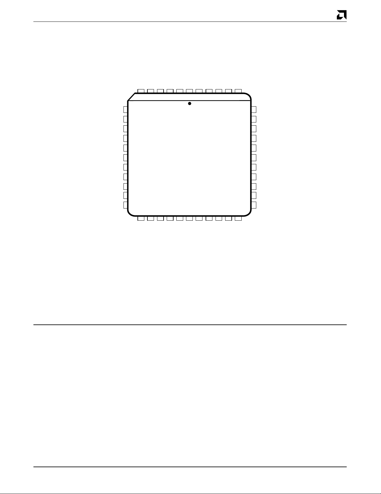
CONNECTION DIAGRAM
Top View
AMD
PLCC
I/O
I/O
I/O
GND
CLK0/I
I/O
I/O
I/O
I/O
10
I
I
11
3
I/O4I/O
561324 4443424140
7
5
8
6
9
7
10
0
11
1
12
13
2
14
8
15
9
16
17
18 282726252423222119 20
13
I/O12I/O
2
I/O
14
I/O
1
I/O
15
I/O
0
I/O
CC
V
GND
GND
CC
V
16
I/O
30
31
I/O
I/O
18
I/O17I/O
28
I/O29I/O
39
38
37
36
35
34
33
32
31
30
29
19
20
I/O
I/O
I/O
27
I/O
26
I/O
25
I/O
24
CLK1/I
GND
I
4
I
3
I/O
23
I/O
22
I/O
21
5
14127I-2
Note:
Pin-compatible with MACH111, MACH210, MACH211, and MACH215.
PIN DESIGNATIONS
CLK/I = Clock or Input
GND = Ground
I = Input
I/O = Input/Output
= Supply Voltage
V
CC
3MACH110-12/15/20
Page 4
AMD
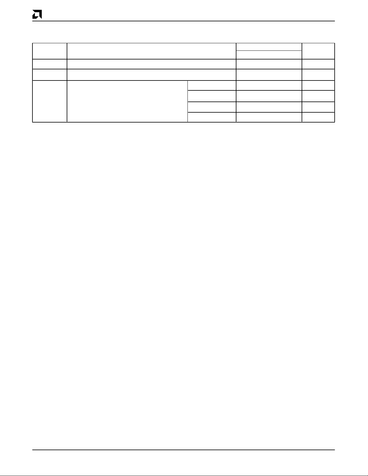
ORDERING INFORMATION
Commercial Products
AMD programmable logic products for commercial applications are available with several ordering options. The order number
(Valid Combination) is formed by a combination of:
FAMILY TYPE
MACH = Macro Array CMOS High-Speed
DEVICE NUMBER
110 = 32 Macrocells, 44 Pins
SPEED
-12 = 12 ns t
-15 = 15 ns t
-20 = 20 ns t
PD
PD
PD
Valid Combinations
MACH110-12
MACH110-15
MACH110-20
JC
MACH -12 J C
110
The Valid Combinations table lists configurations
planned to be supported in volume for this device.
Consult the local AMD sales office to confirm availability
of specific valid combinations and to check on newly
released combinations.
OPTIONAL PROCESSING
Blank = Standard Processing
OPERATING CONDITIONS
C = Commercial (0
PACKAGE TYPE
J = 44-Pin Plastic Leaded
Chip Carrier (PL 044)
Valid Combinations
°C to +70°C)
MACH110-12/15/20 (Com’l)4
Page 5
AMD
ORDERING INFORMATION
Industrial Products
AMD programmable logic products for Industrial applications are available with several ordering options. The order number (Valid
Combination) is formed by a combination of:
FAMILY TYPE
MACH = Macro Array CMOS High-Speed
DEVICE NUMBER
110 = 32 Macrocells, 44 Pins
SPEED
-14 = 14 ns t
-18 = 18 ns t
-24 = 24 ns t
PD
PD
PD
Valid Combinations
MACH110-14
MACH110-18 JI
MACH110-24
MACH -14 I
110
J
The Valid Combinations table lists configurations
planned to be supported in volume for this device.
Consult the local AMD sales office to confirm availability
of specific valid combinations and to check on newly
released combinations.
OPTIONAL PROCESSING
Blank = Standard Processing
OPERATING CONDITIONS
I = Industrial (–40°C to +85°C)
PACKAGE TYPE
J = 44-Pin Plastic Leaded Chip
Carrier (PL 044)
Valid Combinations
5MACH110-14/18/25 (Ind)
Page 6
AMD
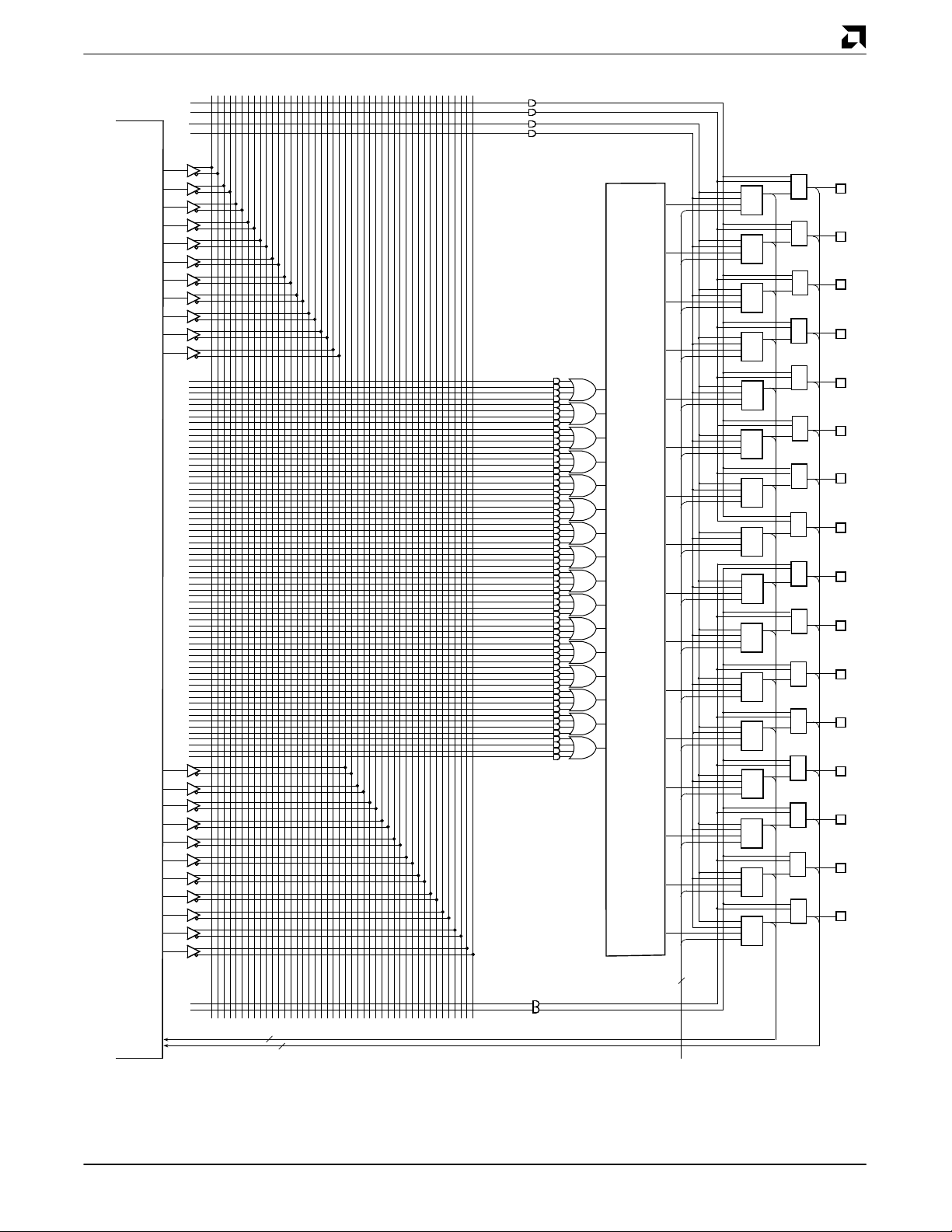
FUNCTIONAL DESCRIPTION
The MACH110 consists of two PAL blocks connected by
a switch matrix. There are 32 I/O pins and 6 dedicated
input pins feeding the switch matrix. These signals are
distributed to the two PAL blocks for efficient design
implementation. There are two clock pins that can also
be used as dedicated inputs.
The PAL Blocks
Each PAL block in the MACH110 (Figure 1) contains a
64-product-term logic array, a logic allocator, 16 macrocells and 16 I/O cells. The switch matrix feeds each PAL
block with 22 inputs. This makes the PAL block look
effectively like an independent “PAL22V16”.
There are four additional output enable product terms in
each PAL block. For purposes of output enable, the 16
I/O cells are divided into 2 banks of 8 macrocells. Each
bank is allocated two of the output enable product terms.
An asynchronous reset product term and an asynchronous preset product term are provided for flip-flop
initialization. All flip-flops within the PAL block are
initialized together.
The Switch Matrix
The MACH110 switch matrix is fed by the inputs and
feedback signals from the PAL blocks. Each PAL block
provides 16 internal feedback signals and 16 I/O
feedback signals. The switch matrix distributes these
signals back to the PAL blocks in an efficient manner
that also provides for high performance. The design
software automatically configures the switch matrix
when fitting a design into the device.
The Product-Term Array
The MACH110 product-term array consists of 64
product terms for logic use, and 6 special-purpose
product terms. Four of the special-purpose product
terms provide programmable output enable, one
provides asynchronous reset, and one provides a
synchronous preset. Two of the output enable product
terms are used for the first eight I/O cells; the other two
control the last eight macrocells.
The Logic Allocator
The logic allocator in the MACH110 takes the 64 logic
product terms and allocates them to the 16 macrocells
as needed. Each macrocell can be driven by up to
12 product terms. The design software automatically
configures the logic allocator when fitting the design into
the device.
Table 1 illustrates which product term clusters are
available to each macrocell within a PAL block. Refer to
Figure 1 for cluster and macrocell numbers.
Table 1. Logic Allocation
Available
Output Macrocell Clusters
M
0
M
1
M
2
M
3
M
4
M
5
M
6
M
7
M
8
M
9
M
10
M
11
M
12
M
13
M
14
M
15
C0, C
1
C0, C1, C
C1, C2, C
C2, C3, C
C3, C4, C
C4, C5, C
C5, C6, C
C6, C
7
C8, C
9
C8, C9, C
C9, C10, C
C10, C11, C
C11, C12, C
C12, C13, C
C13, C14, C
C14, C
15
2
3
4
5
6
7
10
11
12
13
14
15
The Macrocell
The MACH110 macrocells can be configured as either
registered or combinatorial, with programmable polarity. The macrocell provides internal feedback whether
configured as registered or combinatorial. The flip-flops
can be configured as D-type or T-type, allowing for
product-term optimization.
The flip-flops can individually select one of two clock
pins, which are also available as data inputs. The registers are clocked on the LOW-to-HIGH transition of the
clock signal. The flip-flops can also be asynchronously
initialized with the common asynchronous reset and
preset product terms.
The I/O Cell
The I/O cell in the MACH110 consists of a three-state
output buffer. The three-state buffer can be configured
in one of three ways: always enabled, always disabled,
or controlled by a product term. If product term control is
chosen, one of two product terms may be used to
provide the control. The two product terms that are
available are common to eight I/O cells. Within each
PAL block, two product terms are available for selection
by the first eight three-state outputs; two other product
terms are available for selection by the last eight
three-state outputs.
These choices make it possible to use the macrocell as
an output, an input, a bidirectional pin, or a three-state
output for use in driving a bus.
6 MACH110-12/15/20
Page 7
AMD
Switch
Matrix
0 4 8 12 16 20 24 28 40324336
0
63
Output Enable
Output Enable
Asynchronous Reset
Asynchronous Preset
M
M
M
M
C
0
M
C
1
C
2
M
C
3
C
4
M
C
5
C
6
M
C
7
C
Logic Allocator
8
M
C
9
C
10
M
C
11
C
12
M
C
10
13
C
14
C
M
15
11
M
12
M
13
M
14
M
15
I/O
Output
0
1
2
3
4
5
6
7
8
9
Macro
Cell
Output
Macro
Cell
Output
Macro
Cell
Output
Macro
Cell
Output
Macro
Cell
Output
Macro
Cell
Output
Macro
Cell
Output
Macro
Cell
Output
Macro
Cell
Output
Macro
Cell
Output
Macro
Cell
Output
Macro
Cell
Output
Macro
Cell
Output
Macro
Cell
Output
Macro
Cell
Output
Macro
Cell
Cell
I/O
Cell
I/O
Cell
I/O
Cell
I/O
Cell
I/O
Cell
I/O
Cell
I/O
Cell
I/O
Cell
I/O
Cell
I/O
Cell
I/O
Cell
I/O
Cell
I/O
Cell
I/O
Cell
I/O
Cell
I/O
I/O
I/O
I/O
I/O
I/O
I/O
I/O
I/O
I/O
I/O
I/O
I/O
I/O
I/O
I/O
0 4 8 12 16 20 24 28 40324336
16
16
Figure 1. MACH110 PAL Block
Output Enable
Output Enable
CLK
4
14127I-3
7MACH110-12/15/20
Page 8
AMD
ABSOLUTE MAXIMUM RATINGS
Storage Temperature –65°C to +150°C. . . . . . . . . . .
Ambient Temperature
With Power Applied –55°C to +125°C. . . . . . . . . . . . .
Supply Voltage with
Respect to Ground –0.5 V to +7.0 V. . . . . . . . . . . . .
DC Input Voltage –0.5 V to V
DC Output or I/O
Pin Voltage –0.5 V to V
CC
CC
+ 0.5 V. . . . . . . . . . . .
+ 0.5 V. . . . . . . . . . . . . . . .
OPERATING RANGES
Commercial (C) Devices
Ambient Temperature (T
Operating in Free Air 0°C to +70°C. . . . . . . . . . . .
Supply Voltage (V
CC
with Respect to Ground +4.75 V to +5.25 V. . . . .
Operating ranges define those limits between which the functionality of the device is guaranteed.
)
A
)
Static Discharge Voltage 2001 V. . . . . . . . . . . . . . . .
Latchup Current
(T
= 0°C to 70°C) 200 mA. . . . . . . . . . . . . . . . . . . . .
A
Stresses above those listed under Absolute Maximum Ratings
may cause permanent device failure. Functionality at or above
these limits is not implied. Exposure to Absolute Maximum
Ratings for extended periods may affect device reliability. Programming conditions may differ.
DC CHARACTERISTICS over COMMERCIAL operating ranges unless otherwise specified
Parameter
Symbol Parameter Description Test Conditions Min Typ Max Unit
V
V
V
V
I
I
I
I
OH
OL
I
IH
I
IL
OZH
OZL
SC
CC
IH
IL
Output HIGH Voltage IOH = –3.2 mA, VCC = Min 2.4 V
= V
V
or V
IN
IH
IL
Output LOW Voltage IOL = 16 mA, VCC = Min 0.5 V
V
= V
or V
IN
IH
IL
Input HIGH Voltage Guaranteed Input Logical HIGH 2.0 V
Voltage for all Inputs (Note 1)
Input LOW Voltage Guaranteed Input Logical LOW 0.8 V
Voltage for all Inputs (Note 1)
Input HIGH Current VIN = 5.25 V, V
Input LOW Current VIN = 0 V, V
Off-State Output Leakage V
Current HIGH V
Off-State Output Leakage V
Current LOW V
Output Short-Circuit Current V
Supply Current (Typical) V
= 5.25 V, V
OUT
= V
IN
IH
= 0 V, V
OUT
= V
IN
IH
= 0.5 V, V
OUT
= 5 V, T
CC
or VIL (Note 2)
or VIL (Note 2)
= Max (Note 2) 10 µA
CC
= Max (Note 2) –10 µA
CC
= Max 10 µA
CC
= Max –10 µA
CC
= Max (Note 3) –30 –160 mA
CC
=25°C, 95 mA
A
f = 25 MHz (Note 4)
Notes:
1. These are absolute values with respect to device ground and all overshoots due to system and/or tester noise are included.
2. I/O pin leakage is the worst case of I
and I
IL
(or IIH and I
OZL
OZH
).
3. Not more than one output should be shorted at a time. Duration of the short-circuit should not exceed one second.
V
= 0.5 V has been chosen to avoid test problems caused by tester ground degradation.
OUT
4. Measured with a 16-bit up/down counter program. This pattern is programmed in each PAL block and is capable of being
loaded, enabled, and reset.
MACH110-12/15/20 (Com’l)8
Page 9
AMD
CAPACITANCE (Note 1)
Parameter
Symbol Parameter Description Test Conditions Typ Unit
C
IN
C
OUT
Input Capacitance V
Output Capacitance V
= 2.0 V VCC = 5.0 V, TA = 25°C6 pF
IN
= 2.0 V f = 1 MHz 8 pF
OUT
SWITCHING CHARACTERISTICS over COMMERCIAL operating ranges (Note 2)
Parameter
-12 -20
Symbol Parameter Description Min Max Min Max Min Max Unit
t
PD
Input, I/O, or Feedback to Combinatorial 12 15 20 ns
Output (Note 3)
t
S
t
H
t
CO
t
WL
t
WH
Setup Time from Input, I/O, or Feedback
to Clock
Hold Time 0 0 0 ns
Clock to Output (Note 3) 8 10 12 ns
Clock Width
Maximum
f
MAX
Frequency
(Note 1)
t
t
ARW
t
ARR
t
t
APW
t
APR
t
t
AR
AP
EA
ER
Asynchronous Reset to Registered Output 16 20 25 ns
Asynchronous Reset Width (Note 1) 12 15 20 ns
Asynchronous Reset Recovery Time (Note 1) 8 10 15 ns
Asynchronous Preset to Registered Output 16 20 25 ns
Asynchronous Preset Width (Note 1) 12 15 20 ns
Asynchronous Preset Recovery Time (Note 1) 8 10 15 ns
Input, I/O, or Feedback to Output Enable (Note 3) 12 15 20 ns
Input, I/O, or Feedback to Output Disable (Note 3) 12 15 20 ns
External Feedback 1/(t
Internal Feedback (f
CNT
No Feedback 1/(t
D-type
T-type
LOW
HIGH
D-type
+ tCO)
S
T-type
D-type
)
+ tWH) 83.3 83.3 62.5 MHz
WL
T-type
71013ns
81114ns
668ns
668ns
66.7 50 40 MHz
62.5 47.6 38.5 MHz
76.9 66.6 47.6 MHz
71.4 55.5 43.5 MHz
-15
Notes:
1. These parameters are not 100% tested, but are evaluated at initial characterization and at any time the design is modified
where capacitance may be affected.
2. See Switching Test Circuit, for test conditions.
3. Parameters measured with 16 outputs switching.
9MACH110-12/15/20 (Com’l)
Page 10

AMD
ABSOLUTE MAXIMUM RATINGS
Storage Temperature –65°C to +150°C. . . . . . . . . . .
Ambient Temperature
With Power Applied –55°C to +125°C. . . . . . . . . . . . .
Supply Voltage with
INDUSTRIAL OPERATING RANGES
Ambient Temperature (TA)
Operating in Free Air –40°C to +85°C. . . . . . . . . . . .
Supply Voltage (V
with Respect to Ground +4.5 V to +5.5 V. . . . . . . . . .
CC)
Respect to Ground –0.5 V to +7.0 V. . . . . . . . . . . . .
DC Input Voltage –0.5 V to V
CC
+ 0.5 V. . . . . . . . . . . .
Operating ranges define those limits between which the functionality of the device is guaranteed.
DC Output or I/O
CC
Pin Voltage –0.5 V to V
+ 0.5 V. . . . . . . . . . . . . . . .
Static Discharge Voltage 2001 V. . . . . . . . . . . . . . . .
Latchup Current
(T
A = –40°C to +85°C) 200 mA. . . . . . . . . . . . . . . . . .
Stresses above those listed under Absolute Maximum Ratings
may cause permanent device failure. Functionality at or above
these limits is not implied. Exposure to Absolute Maximum
Ratings for extended periods may affect device reliability.
Programming conditions may differ.
DC CHARACTERISTICS over INDUSTRIAL operating ranges unless otherwise specified
Parameter
Symbol Parameter Description Test Conditions Min Typ Max Unit
VOH Output HIGH Voltage IOH = –3.2 mA, VCC = Min 2.4 V
VIN = VIH or VIL
VOL Output LOW Voltage IOL = 16 mA, VCC = Min 0.5 V
VIN = VIH or VIL
VIH Input HIGH Voltage Guaranteed Input Logical HIGH 2.0 V
Voltage for all Inputs (Note 1)
VIL Input LOW Voltage Guaranteed Input Logical LOW 0.8 V
Voltage for all Inputs (Note 1)
IIH Input HIGH Current VIN = 5.25 V, VCC
IIL Input LOW Current VIN = 0 V, VCC
IOZH Off-State Output Leakage VOUT
Current HIGH VIN = VIH or VIL (Note 2)
IOZL Off-State Output Leakage VOUT = 0 V, VCC
Current LOW VIN = VIH or VIL (Note 2)
ISC Output Short-Circuit Current VOUT = 0.5 V, VCC
ICC
Notes:
1. These are absolute values with respect to device ground and all overshoots due to system and/or tester noise are included.
2. I/O pin leakage is the worst case of I
3. Not more than one output should be shorted at a time. Duration of the short-circuit should not exceed one second.
V
OUT
= 0.5 V has been chosen to avoid test problems caused by tester ground degradation.
4. Measured with a 16-bit up/down counter pattern. This pattern is programmed in each PAL block and is capable of
being loaded, enabled, and reset.
Supply Current (Typical) VCC = 5 V, TA = 25°C, f = 25 MHz (Note 4) 95 mA
IL
and I
OZL
(or IIH and I
= 5.25 V, VCC = Max 10 µA
OZH
= Max (Note 2) 10 µA
= Max (Note 2) –10 µA
= Max –10 µA
= Max (Note 3) –30 –160 mA
).
MACH110-14/18/20 (Ind)10
Page 11

AMD
CAPACITANCE (Note 1)
Parameter
Symbol Parameter Description Test Conditions Typ Unit
CIN Input Capacitance VIN
COUT Output Capacitance VOUT = 2.0 V f = 1 MHz 8 pF
= 2.0 V VCC = 5.0 V, TA = 25°C6pF
SWITCHING CHARACTERISTICS over INDUSTRIAL operating ranges (Note 2)
Parameter
Symbol Parameter Description Min Max Min Max Min Max Unit
PD Input, I/O, or Feedback to Combinatorial 14.5 18 24 ns
t
Output (Note 3)
t
S
H Hold Time 0 0 0 ns
t
tCO Clock to Output (Note 3) 10 12 14.5 ns
WL 7.5 7.5 10 ns
t
WH 7.5 7.5 10 ns
t
MAX 61.5 53 38 MHz
f
AR Asynchronous Reset to Registered Output 19.5 24 30 ns
t
ARW Asynchronous Reset Width (Note 1) 14.5 18 24 ns
t
ARR Asynchronous Reset Recovery Time (Note 1) 10 12 18 ns
t
AP Asynchronous Preset to Registered Output 19.5 24 30 ns
t
APW Asynchronous Preset Width (Note 1) 14.5 18 24 ns
t
APR Asynchronous Preset Recovery Time (Note 1) 10 12 18 ns
t
EA Input, I/O, or Feedback to Output Enable (Note 3) 14.5 18 24 ns
t
tER Input, I/O, or Feedback to Output Disable (Note 3) 14.5 18 24 ns
Setup Time from Input, I/O, or Feedback
to Clock
Clock Width
External Feedback 1/(t
Maximum
Frequency
(Note 1)
Internal Feedback (f
No Feedback 1/(t
CNT)
S
+ tCO)
WL + tWH) 66.5 66.5 50 MHz
D-type
T-type
LOW
HIGH
D-type
T-type
D-type
T-type
-14 -24
8.5 12 16 ns
10 13.5 17 ns
53.5 40 32 MHz
50 38 30 MHz
57 44 34.5 MHz
Notes:
1. These parameters are not 100% tested, but are evaluated at initial characterization and at any time the design is modified
where capacitance may be affected.
2. See Switching Test Circuit, for test conditions.
3. Parameters measured with 16 outputs switching.
-18
11MACH110-14/18/20 (Ind)
Page 12

AMD
TYPICAL CURRENT VS. VOLTAGE (I-V) CHARACTERISTICS
V
= 5.0 V, TA = 25°C
CC
(mA)
I
OL
80
60
40
20
–0.8 –0.6 –0.4 .2–0.2–1.0
–20
–40
–60
–80
.4 .6 1.0.8
V
(V)
OL
–3 –2 –1
–100
–125
–150
Output, HIGH
Output, LOW
I
(mA)
OH
25
–25
–50
–75
I
20
(mA)
I
123
45
14127I-4
V
(V)
OH
14127I-5
–2 –1
123
–20
–40
–60
–80
–100
Input
12 MACH110-12/15/20
45
V
(V)
I
14127I-6
Page 13

TYPICAL ICC CHARACTERISTICS
V
= 5 V, TA = 25°C
CC
150
125
100
AMD
MACH110
ICC (mA)
The selected “typical” pattern is a 16-bit up/down counter. This pattern is programmed in each PAL block and is capable of
being loaded, enabled, and reset.
Maximum frequency shown uses internal feedback and a D-type register.
75
50
25
0
0 102030405060708090
Frequency (MHz)
14127I-7
13MACH110-12/15/20
Page 14
AMD
TYPICAL THERMAL CHARACTERISTICS
Measured at 25°C ambient. These parameters are not tested.
Parameter
Symbol Parameter Description PLCC Unit
Typ
θ
jc
θ
ja
θ
jma
Thermal impedance, junction to case 14 °C/W
Thermal impedance, junction to ambient 39 °C/W
Thermal impedance, junction to 200 lfpm air 33 °C/W
ambient with air flow
400 lfpm air 30 °C/W
600 lfpm air 27 °C/W
800 lfpm air 25 °C/W
Plastic θjc Considerations
The data listed for plastic θjc are for reference only and are not recommended for use in calculating junction temperatures. The
θ
heat-flow paths in plastic-encapsulated devices are complex, making the
package surface. Tests indicate this measurement reference point is directly below the die-attach area on the bottom center of the
package. Furthermore,
θ
jc tests on packages are performed in a constant-temperature bath, keeping the package surface at a
constant temperature. Therefore, the measurements can only be used in a similar environment.
jc measurement relative to a specific location on the
14 MACH110-12/15/20
Page 15

SWITCHING WAVEFORMS
AMD
Input, I/O,
or Feed-
back
Clock
Registered
Output
Input, I/O, or
Feedback
Combinatorial
Output
t
S
V
T
Registered Output
t
CO
t
H
V
T
Combinatorial Output
Input, I/O, or
Feedback
V
T
14127I-9
Latched
V
T
Gate
Out
t
PD
V
T
14127I-8
V
T
t
t
HL
SL
V
T
t
PDL
t
GO
V
T
14127I-10
Latched Output (MACH 2, 3, and 4)
t
WH
Clock
Clock Width
Registered
Input
t
SIR
Input
Register
Clock
Combinatorial
Output
Registered Input (MACH 2 and 4)
Notes:
= 1.5 V.
1. V
T
2. Input pulse amplitude 0 V to 3.0 V.
3. Input rise and fall times 2 ns–4 ns typical.
t
WL
V
T
t
ICO
14127I-11
Gate
t
GWS
V
T
14127I-12
Gate Width (MACH 2, 3, and 4)
V
t
T
HIR
Registered
Input
V
T
Input
Register
V
T
Clock
t
V
T
Output
Register
14127I-13 14127I-14
Clock
ICS
V
T
Input Register to Output Register Setup
(MACH 2 and 4)
15MACH110-12/15/20
Page 16

AMD
SWITCHING WAVEFORMS
Latched
Combinatorial
In
Latched
Gate
Output
V
t
HIL
T
V
T
t
IGO
V
T
14127I-15
In
t
SIL
Latched Input (MACH 2 and 4)
t
PDLL
V
T
Latched
Out
t
Input
IGOL
Latch Gate
t
IGS
Output
Latch Gate
Notes:
1. VT = 1.5 V.
2. Input pulse amplitude 0 V to 3.0 V.
3. Input rise and fall times 2 ns–4 ns typical.
Latched Input and Output
(MACH 2, 3, and 4)
V
T
t
SLL
V
T
14127I-16
16 MACH110-12/15/20
Page 17

SWITCHING WAVEFORMS
t
WICH
Clock
Input Register Clock Width
(MACH 2 and 4)
t
WICL
V
T
14127I-17
Input
Latch
Gate
t
WIGL
Input Latch Gate Width
(MACH 2 and 4)
AMD
V
T
14127I-18
Input, I/O, or
Feedback
Registered
Output
Clock
t
ARW
t
AR
V
T
Asynchronous Reset
Input, I/O, or
Feedback
Outputs
V
T
t
ARR
V
T
14127I-19
t
ER
Input, I/O,
or Feedback
Registered
Output
Clock
V
- 0.5V
OH
+ 0.5V
V
OL
t
APW
V
T
t
AP
V
T
t
APR
V
T
14127I-20
Asynchronous Preset
V
T
t
EA
V
T
Notes:
= 1.5 V.
1. V
T
2. Input pulse amplitude 0 V to 3.0 V.
3. Input rise and fall times 2 ns–4 ns typical.
14127I-21
Output Disable/Enable
17MACH110-12/15/20
Page 18

AMD
KEY TO SWITCHING WAVEFORMS
WAVEFORM INPUTS OUTPUTS
SWITCHING TEST CIRCUIT
Must be
Steady
May
Change
from H to L
May
Change
from L to H
Don’t Care,
Any Change
Permitted
Does Not
Apply
5 V
Will be
Steady
Will be
Changing
from H to L
Will be
Changing
from L to H
Changing,
State
Unknown
Center
Line is HighImpedance
“Off” State
KS000010-PAL
S
1
R
1
Specification S
, t
t
PD
CO
t
EA
Output
R
2
Commercial
1
C
L
R
1
Closed 1.5 V
Z → H: Open 35 pF 1.5 V
C
L
Test Point
R
2
14127I-22
Measured
Output Value
Z → L: Closed 300 Ω 390 Ω
t
ER
H →Z: Open 5 pF H →Z: VOH – 0.5 V
L →Z: Closed L →Z: V
*Switching several outputs simultaneously should be avoided for accurate measurement.
+ 0.5 V
OL
18 MACH110-12/15/20
Page 19

f
PARAMETERS
MAX
The parameter f
is the maximum clock rate at which
MAX
the device is guaranteed to operate. Because the flexibility inherent in programmable logic devices offers a
choice of clocked flip-flop designs, f
is specified for
MAX
three types of synchronous designs.
The first type of design is a state machine with feedback
signals sent off-chip. This external feedback could go
back to the device inputs, or to a second device in a
multi-chip state machine. The slowest path defining the
period is the sum of the clock-to-output time and the input setup time for the external signals (t
ciprocal, f
, is the maximum frequency with external
MAX
+ tCO). The re-
S
feedback or in conjunction with an equivalent speed device. This f
is designated “f
MAX
external.”
MAX
The second type of design is a single-chip state machine with internal feedback only. In this case, flip-flop
inputs are defined by the device inputs and flip-flop outputs. Under these conditions, the period is limited by the
internal delay from the flip-flop outputs through the internal feedback and logic to the flip-flop inputs. This f
designated “f
internal”. A simple internal counter is a
MAX
MAX
is
good example of this type of design; therefore, this parameter is sometimes called “f
CNT.
”
AMD
The third type of design is a simple data path application. In this case, input data is presented to the flip-flop
and clocked through; no feedback is employed. Under
these conditions, the period is limited by the sum of the
data setup time and the data hold time (t
a lower limit for the period of each f
mum clock period (t
+ tWL). Usually, this minimum
WH
clock period determines the period for the third f
ignated “f
no feedback.”
MAX
For devices with input registers, one additional f
rameter is specified: f
. Because this involves no
MAXIR
feedback, it is calculated the same way as f
+ tH). However,
S
type is the mini-
MAX
MAX
no feed-
MAX
, des-
MAX
pa-
back. The minimum period will be limited either by the
+ t
sum of the setup and hold times (t
the clock widths (t
WICL
+ t
WICH
SIR
). The clock widths are normally the limiting parameters, so that f
as 1/(t
WICL
+ t
). Note that if both input and output reg-
WICH
) or the sum of
HIR
is specified
MAXIR
isters are use in the same path, the overall frequency will
be limited by t
All frequencies except f
other measured AC parameters. f
ICS
.
internal are calculated from
MAX
internal is meas-
MAX
ured directly.
CLK
(SECOND
CHIP)
LOGIC REGISTER
tt
SCO
f
External; 1/(tS + tCO)
MAX
t
S
CLK
LOGIC REGISTER
CLK
LOGIC REGISTER
f
Internal (f
MAX
CNT
)
CLK
REGISTER
LOGIC
t
S
f
No Feedback; 1/(tS + tH) or 1/(tWH + tWL)
MAX
t
SIR
f
MAXIR
t
HIR
; 1/(t
SIR
+ t
HIR
) or 1/(t
WICL
+ t
WICH
14127I-23
)
19MACH110-12/15/20
Page 20

AMD
ENDURANCE CHARACTERISTICS
The MACH families are manufactured using AMD’s
advanced Electrically Erasable process. This technology uses an EE cell to replace the fuse link used in
bipolar parts. As a result, the device can be erased and
reprogrammed, a feature which allows 100% testing at
the factory.
Endurance Characteristics
Parameter
Symbol Parameter Description Min Units Test Conditions
10 Years Max Storage
Temperature
t
DR
N Max Reprogramming Cycles 100 Cycles Normal Programming
Min Pattern Data Retention Time
20 Years Max Operating
Temperature
Conditions
20 MACH110-12/15/20
Page 21

INPUT/OUTPUT EQUIVALENT SCHEMATICS
1 kΩ
ESD
Protection
Input
AMD
V
CC
100 kΩ
V
CC
V
CC
Preload
Circuitry
100 kΩ
Feedback
Input
I/O
V
CC
1 kΩ
14127I-24
21MACH110-12/15/20
Page 22

AMD
POWER-UP RESET
The MACH devices have been designed with the capability to reset during system power-up. Following powerup, all flip-flops will be reset to LOW. The output state
wide range of ways V
conditions are required to insure a valid power-up reset.
These conditions are:
will depend on the logic polarity. This feature provides
extra flexibility to the designer and is especially valuable
in simplifying state machine initialization. A timing diagram and parameter table are shown below. Due to the
synchronous operation of the power-up reset and the
Parameter
Symbol Parameter Descriptions Max Unit
1. The V
2. Following reset, the clock input must not be driven
from LOW to HIGH until all applicable input and
feedback setup times are met.
rise must be monotonic.
CC
can rise to its steady state, two
CC
t
PR
t
S
t
WL
Registered
Power
Output
Clock
Power-Up Reset Time 10 µs
Input or Feedback Setup Time
Clock Width LOW
4 V
t
PR
t
S
t
WL
See
Switching
Characteristics
V
CC
14127I-25
Power-Up Reset Waveform
22 MACH110-12/15/20
Page 23

USING PRELOAD AND OBSERVABILITY
In order to be testable, a circuit must be both controllable
and observable. To achieve this, the MACH devices
incorporate register preload and observability.
In preload mode, each flip-flop in the MACH device can
be loaded from the I/O pins, in order to perform
functional testing of complex state machines. Register
preload makes it possible to run a series of tests from a
known starting state, or to load illegal states and test for
proper recovery. This ability to control the MACH
device’s internal state can shorten test sequences,
since it is easier to reach the state of interest.
The observability function makes it possible to see the
internal state of the buried registers during test by
overriding each register’s output enable and activating
the output buffer. The values stored in output and buried
registers can then be observed on the I/O pins. Without
this feature, a thorough functional test would be
impossible for any designs with buried registers.
While the implementation of the testability features is
fairly straightforward, care must be taken in certain
instances to insure valid testing.
Preloaded
HIGH
DQQ
1
AR
Preloaded
HIGH
Q
D
2
Q
AR
AMD
One case involves asynchronous reset and preset. If the
MACH registers drive asynchronous reset or preset
lines and are preloaded in such a way that reset or
preset are asserted, the reset or preset may remove the
preloaded data. This is illustrated in Figure 2. Care
should be taken when planning functional tests, so that
states that will cause unexpected resets and presets are
not preloaded.
Another case to be aware of arises in testing combinatorial logic. When an output is configured as combinatorial, the observability feature forces the output into
registered mode. When this happens, all product terms
are forced to zero, which eliminates all combinatorial
data. For a straight combinatorial output, the correct
value will be restored after the preload or observe
function, and there will be no problem. If the function
implements a combinatorial latch, however, it relies on
feedback to hold the correct value, as shown in Figure 3.
As this value may change during the preload or observe
operation, you cannot count on the data being correct
after the operation. To insure valid testing in these
cases, outputs that are combinatorial latches should not
be tested immediately following a preload or observe
sequence, but should first be restored to a known state.
Preload
Mode
Q
1
AR
Q
2
Set
On
Off
Figure 2. Preload/Reset Conflict
14127I-26
All MACH 2 devices support both preload and
observability.
Contact individual programming vendors in order to
verify programmer support.
Reset
Figure 3. Combinatorial Latch
14127I-27
23MACH110-12/15/20
Page 24

AMD
DEVELOPMENT SYSTEMS (subject to change)
For more information on the products listed below, please consult the AMD FusionPLD Catalog.
MANUFACTURER SOFTWARE DEVELOPMENT SYSTEMS
Advanced Micro Devices, Inc.
P.O. Box 3453, MS 1028
Sunnyvale, CA 94088-3543
(800) 222-9323 or (408) 732-2400
Advanced Micro Devices, Inc.
P.O. Box 3453, MS 1028
Sunnyvale, CA 94088-3543
(800) 222-9323 or (408) 732-2400
Advanced Micro Devices, Inc.
P.O. Box 3453, MS 1028
Sunnyvale, CA 94088-3543
(800) 222-9323 or (408) 732-2400
Advanced Micro Devices, Inc.
P.O. Box 3453, MS 1028
Sunnyvale, CA 94088-3543
(800) 222-9323 or (408) 732-2400
Cadence Design Systems
555 River Oaks Pkwy
San Jose, CA 95134
(408) 943-1234
Capilano Computing
960 Quayside Dr., Suite 406
New Westminster, B.C.
Canada V3M 6G2
(800) 444-9064 or (604) 552-6200
MACHXL Software
Ver. 2.0
Design Center/AMD
Software
AMD-ABEL Software
Data I/O MACH Fitters
PROdeveloper/AMD
Software
PROsynthesis/AMD Software
TM
ComposerPIC
Designer
(Requires MACH Fitter)
Verilog, LeapFrog, RapidSim Simulators
(Models also available from Logic Modeling)
Ver. 3.3
MacABEL
TM
Software
(Requires SmartPart MACH Fitter)
CINA, Inc.
P.O. Box 4872
Mountain View, CA 94040
(415) 940-1723
Data I/O Corporation
10525 Willows Road N.E.
P.O. Box 97046
Redmond, WA 98073-9746
(800) 332-8246 or (206) 881-6444
iNt GmbH
Busenstrasse 6
D-8033 Martinsried, Munich, Germany
(89) 857-6667
ISDATA GmbH
Daimlerstr. 51
D7500 Karlsruhe 21 Germany
Germany: 0721/75 10 87
U.S.: (510) 531-8553
Logic Modeling
19500 NW Gibbs Dr.
P.O. Box 310
Beaverton, OR 97075
(503) 690-6900
Logical Devices, Inc.
692 S. Military Trail
Deerfield Beach, FL 33442
(800) 331-7766 or (305) 428-6868
SmartCAT Circuit Analyzer
TM
-5 Software
ABEL
(Requires MACH Fitter)
TM
Synario
Software
PLDSim 90
LOG/iCTM Software
(Requires MACH Fitter)
SmartModelLibrary
CUPLTM Software
24 MACH110-12/15/20
Page 25

DEVELOPMENT SYSTEMS (subject to change) (continued)
MANUFACTURER SOFTWARE DEVELOPMENT SYSTEMS
Mentor Graphics Corp.
8005 S.W. Boeckman Rd.
Wilsonville, OR 97070-7777
(800) 547-3000 or (503) 685-7000
PLDSynthesis
(Requires MACH Fitter)
QuickSim Simulator
(Models also available from Logic Modeling)
TM
AMD
MicroSim Corp.
20 Fairbanks
Irvine, CA 92718
(714) 770-3022
MINC Incorporated
6755 Earl Drive, Suite 200
Colorado Springs, CO 80918
(800) 755-FPGA or (719) 590-1155
OrCAD
3175 N.W. Aloclek Dr.
Hillsboro, OR 97124
(503) 690-9881
SUSIE–CAD
10000 Nevada Highway, Suite 201
Boulder City, NV 89005
(702) 293-2271
Teradyne EDA
321 Harrison Ave.
Boston, MA 02118
(800) 777-2432 or (617) 422-2793
Viewlogic Systems, Inc.
293 Boston Post Road West
Marlboro, MA 01752
(800) 442-4660 or (508) 480-0881
Design Center Software
(Requires MACH Fitter)
PLDesignerTM-XL Software
(Requires MACH Fitter)
Programmable Logic Design Tools 386+
Schematic Design Tool 386+
Digital Simulation Tools
TM
SUSIE
MultiSIM Interactive Simulator
ViewPLD or PROPLD
(Requires PROSim Simulator MACH Fitter)
ViewSim Simulator
(Models for ViewSim also available
from Logic Modeling)
Simulator
LASAR
MANUFACTURER TEST GENERATION SYSTEM
Acugen Software, Inc.
427-3 Amherst St., Suite 391
Nashua, NH 03063
(603) 891-1995
iNt GmbH
Busenstrasse 6
D-8033 Martinsried, Munich, Germany
(87) 857-6667
Advanced Micro Devices is not responsible for any information relating to the products of third parties. The inclusion of such information is not a representation nor
an endorsement by AMD of these products.
ATGENTM Test Generation Software
PLDCheck 90
25MACH110-12/15/20
Page 26

AMD
APPROVED PROGRAMMERS (subject to change)
For more information on the products listed below, please consult the AMD FusionPLD Catalog.
MANUFACTURER PROGRAMMER CONFIGURATION
Advin Systems, Inc.
1050-L East Duane Ave.
Sunnyvale, CA 94086
(408) 243-7000
BP Microsystems
100 N. Post Oak Rd.
Houston, TX 77055-7237
(800) 225-2102 or (713) 688-4600
Data I/O Corporation
10525 Willows Road N.E.
P.O. Box 97046
Redmond, WA 98073-9746
(800) 332-8246 or (206) 881-6444
Logical Devices Inc./Digelec
692 S. Military Trail
Deerfield Beach, FL 33442
(800) 331-7766 or (305) 428-6868
SMS North America, Inc.
16522 NE 135th Place
Redmond, WA 98052
(800) 722-4122
or
SMS
lm Grund 15
D-7988 Vangen Im Allgau, Germany
07522-5018
UniSite
TM
Pilot U84
BP1200
Model 3900
ALLPROTM–88
Sprint/Expert
AutoSite
Stag Microsystems Inc.
1600 Wyatt Dr. Suite 3
Santa Clara, CA 95054
(408) 988-1118
or
Stag House
Martinfield, Welwyn Garden City
Herfordshire UK AL7 1JT
707-332148
System General
510 S. Park Victoria Dr.
Milpitas, CA 95035
(408) 263-6667
or
3F, No. 1, Alley 8, Lane 45
Bao Shing Rd., Shin Diau
Taipei, Taiwan
2-917-3005
Stag Quazar
Turpro-1
APPROVED ON-BOARD PROGRAMMERS
MANUFACTURER PROGRAMMER CONFIGURATION
Corelis, Inc.
12607 Hidden Creek Way, Suite H
Cerritos, California 70703
(310) 926-6727
Advanced Micro Devices
P.O. Box 3453, MS-1028
Sunnyvale, CA 94088-3453
(800) 222-9323
JTAG PROG
MACHpro
26 MACH110-12/15/20
Page 27

PROGRAMMER SOCKET ADAPTERS (subject to change)
MANUFACTURER PART NUMBER
EDI Corporation
P.O. Box 366
Patterson, CA 95363
(209) 892-3270
Emulation Technology
2344 Walsh Ave., Bldg. F
Santa Clara, CA 95051
(408) 982-0660
Logical Systems Corp.
P.O. Box 6184
Syracuse, NY 13217-6184
(315) 478-0722
Procon Technologies, Inc.
1333 Lawrence Expwy, Suite 207
Santa Clara, CA 95051
(408) 246-4456
Contact Manufacturer
Contact Manufacturer
Contact Manufacturer
Contact Manufacturer
AMD
27MACH110-12/15/20
Page 28

AMD
PHYSICAL DIMENSIONS*
PL 044
44-Pin Plastic Leaded Chip Carrier (measured in inches)
.685
.695
.650
.656
.042
.056
.062
.083
.685
.695
.650
.656
.026
.032
Pin 1 I.D.
TOP VIEW
.050 REF
.009
.015
*For reference only. BSC is an ANSI standard for Basic Space Centering.
.090
.120
.165
.180
SIDE VIEW
.590
.500
.630
REF
.013
.021
SEATING PLANE
16-038-SQ
PL 044
DA78
6-28-94 ae
Trademarks
Copyright 1995 Advanced Micro Devices, Inc. All rights reserved.
AMD, the AMD logo, MACH, and PAL are registered trademarks of Advanced Micro Devices, Inc.
Product names used in this publication are for identification purposes only and may be trademarks of their respective companies.
28 MACH110-12/15/20
 Loading...