

Page 1

AMD Geode™ LX Processor/
CS5536 Companion Device
GeodeROM Porting Guide
April 2006
Publication ID: 40680B
AMD Geode™ LX Processor/CS5536 Companion Device GeodeROM Porting Guide 1
Page 2

© 2006 Advanced Micro Devices, Inc. All rights reserved.
The contents of this document are provided in connection with Advanced Micro
Devices, Inc. (“AMD”) products. AMD makes no representations or warranties with
respect to the accuracy or completeness of the contents of this publication and
reserves the right to make changes to specifications and product descriptions at
any time without notice. No license, whether express, implied, arising by estoppel
or otherwise, to any intellectual property rights is granted by this publication.
Except as set forth in AMD’s Standard Terms and Conditions of Sale, AMD
assumes no liability whatsoever, and disclaims any express or implied warranty,
relating to its products including, but not limited to, the implied warranty of merchantability, fitness for a particular purpose, or infringement of any intellectual
property right.
AMD’s products are not designed, intended, authorized or warranted for use as
components in systems intended for surgical implant into the body, or in other
applications intended to support or sustain life, or in any other application in which
the failure of AMD’s product could create a situation where personal injury, death,
or severe property or environmental damage may occur. AMD reserves the right to
discontinue or make changes to its products at any time without notice.
Trademarks
AMD, the AMD Arrow logo, and combinations thereof, and Geode, GeodeLink, Virtual System Architecture, and
XpressGRAPHICS are trademarks of Advanced Micro Devices, Inc.
Windows is a registered trademark of Microsoft Corporation in the United States and/or other jurisdictions.
Other product names used in this publication are for identification purposes only and may be trademarks of their respective
companies.
2 AMD Geode™ LX Processor/CS5536 Companion Device GeodeROM Porting Guide
Page 3

Contents 40680B
Contents
List of Figures . . . . . . . . . . . . . . . . . . . . . . . . . . . . . . . . . . . . . . . . . . . . . . . . . . . . . . . . . . 5
List of Tables . . . . . . . . . . . . . . . . . . . . . . . . . . . . . . . . . . . . . . . . . . . . . . . . . . . . . . . . . . . 7
1.0 Overview . . . . . . . . . . . . . . . . . . . . . . . . . . . . . . . . . . . . . . . . . . . . . . . . . . . . . . . . . . 9
1.1 Introduction . . . . . . . . . . . . . . . . . . . . . . . . . . . . . . . . . . . . . . . . . . . . . . . . . . . . . . . . . . . . . . . . . 9
1.2 Assumptions . . . . . . . . . . . . . . . . . . . . . . . . . . . . . . . . . . . . . . . . . . . . . . . . . . . . . . . . . . . . . . . . 9
2.0 Model Specific Registers . . . . . . . . . . . . . . . . . . . . . . . . . . . . . . . . . . . . . . . . . . . 11
2.1 Example MSR Transaction . . . . . . . . . . . . . . . . . . . . . . . . . . . . . . . . . . . . . . . . . . . . . . . . . . . . 11
3.0 GeodeLink™ Architecture . . . . . . . . . . . . . . . . . . . . . . . . . . . . . . . . . . . . . . . . . . . 13
3.1 GeodeLink™ MSR Addressing . . . . . . . . . . . . . . . . . . . . . . . . . . . . . . . . . . . . . . . . . . . . . . . . . 14
3.2 Descriptors . . . . . . . . . . . . . . . . . . . . . . . . . . . . . . . . . . . . . . . . . . . . . . . . . . . . . . . . . . . . . . . . . 14
4.0 Initialization . . . . . . . . . . . . . . . . . . . . . . . . . . . . . . . . . . . . . . . . . . . . . . . . . . . . . . 15
4.1 Processor Initialization . . . . . . . . . . . . . . . . . . . . . . . . . . . . . . . . . . . . . . . . . . . . . . . . . . . . . . . . 15
4.2 AMD Geode™ CS5536 Companion Device Initialization . . . . . . . . . . . . . . . . . . . . . . . . . . . . . 20
4.3 Virtual System Architecture™ Initialization . . . . . . . . . . . . . . . . . . . . . . . . . . . . . . . . . . . . . . . . 24
4.4 PCI Bus Initialization . . . . . . . . . . . . . . . . . . . . . . . . . . . . . . . . . . . . . . . . . . . . . . . . . . . . . . . . . 24
4.5 Miscellaneous Initializations . . . . . . . . . . . . . . . . . . . . . . . . . . . . . . . . . . . . . . . . . . . . . . . . . . . 25
5.0 Implementation . . . . . . . . . . . . . . . . . . . . . . . . . . . . . . . . . . . . . . . . . . . . . . . . . . . 27
5.1 Implementation . . . . . . . . . . . . . . . . . . . . . . . . . . . . . . . . . . . . . . . . . . . . . . . . . . . . . . . . . . . . . 27
6.0 Setup Options . . . . . . . . . . . . . . . . . . . . . . . . . . . . . . . . . . . . . . . . . . . . . . . . . . . . 29
7.0 Memory Map . . . . . . . . . . . . . . . . . . . . . . . . . . . . . . . . . . . . . . . . . . . . . . . . . . . . . . 31
Appendix A Support Documentation . . . . . . . . . . . . . . . . . . . . . . . . . . . . . . . . . . . . . 35
A.1 Document Revision History . . . . . . . . . . . . . . . . . . . . . . . . . . . . . . . . . . . . . . . . . . . . . . . . . . . 35
AMD Geode™ LX Processor/CS5536 Companion Device GeodeROM Porting Guide 3
Page 4

40680B
Contents
4 AMD Geode™ LX Processor/CS5536 Companion Device GeodeROM Porting Guide
Page 5

List of Figures 40680B
List of Figures
Figure 3-1. GeodeLink™ Architecture Topology . . . . . . . . . . . . . . . . . . . . . . . . . . . . . . . . . . . . . . . . . . . 13
Figure 4-1. Clock Control . . . . . . . . . . . . . . . . . . . . . . . . . . . . . . . . . . . . . . . . . . . . . . . . . . . . . . . . . . . . . 15
Figure 7-1. GLIU Descriptor Map . . . . . . . . . . . . . . . . . . . . . . . . . . . . . . . . . . . . . . . . . . . . . . . . . . . . . . . 31
Figure 7-2. CPU Core Cache Descriptors . . . . . . . . . . . . . . . . . . . . . . . . . . . . . . . . . . . . . . . . . . . . . . . . 31
Figure 7-3. CPU Core Cache Region Configurations . . . . . . . . . . . . . . . . . . . . . . . . . . . . . . . . . . . . . . . . 32
Figure 7-4. GeodeROM Flow - LX Processor/CS5536 Device . . . . . . . . . . . . . . . . . . . . . . . . . . . . . . . . 33
AMD Geode™ LX Processor/CS5536 Companion Device GeodeROM Porting Guide 5
Page 6

40680B
List of Figures
6 AMD Geode™ LX Processor/CS5536 Companion Device GeodeROM Porting Guide
Page 7

List of Tables 40680B
List of Tables
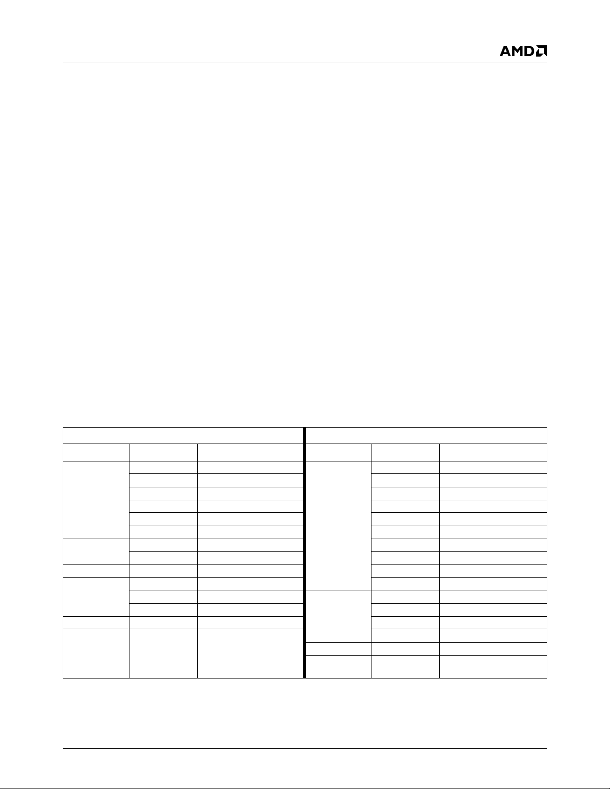
Table 4-1. Default Region Configuration Properties Bit Descriptions . . . . . . . . . . . . . . . . . . . . . . . . . . . 18
Table 4-2. Diverse Device I/O Locations . . . . . . . . . . . . . . . . . . . . . . . . . . . . . . . . . . . . . . . . . . . . . . . . . 23
AMD Geode™ LX Processor/CS5536 Companion Device GeodeROM Porting Guide 7
Page 8

40680B
List of Tables
8 AMD Geode™ LX Processor/CS5536 Companion Device GeodeROM Porting Guide
Page 9

Overview 40680B
1.0Overview
1
1.1 Introduction
This document describes the changes needed for GeodeROM and other BIOSs to support the AMD Geode™ LX processor
and the AMD Geode™ CS5536 companion device. GeodeROM requires modifications for hardware initialization and specific implementations.
Each section targets the GeodeROM changes needed to support the Geode LX processor/CS5536 device system. Where
appropriate, the changes list the “Entry Conditions” that briefly describe the machine state required to execute that function,
as well as some pseudo code for implementing the changes.
For more information on GeodeROM, see the AMD Geode™ GeodeROM Functional Specification (publication ID 32087).
1.2 Assumptions
The following assumptions must be made clear during the design phase.
GeodeROM expects all memory has a serial presence detect (SPD) to determine characteristics for memory controller initialization. If a SPD is not present, GeodeROM outputs a POST code and halts, unless customizations have been made for
the platform.
AMD Geode™ LX Processor/CS5536 Companion Device GeodeROM Porting Guide 9
Page 10

40680B
Overview
10 AMD Geode™ LX Processor/CS5536 Companion Device GeodeROM Porting Guide
Page 11

Model Specific Registers 40680B
2.0Model Specific Registers
2
There are two ways to read or write Model Specific Registers (MSRs) in an AMD Geode™ LX processor-based system.
Software running on the processor can use the RDMSR and WRMSR instructions, and modules within the processor can
use the GeodeLink™ MSR transactions. The second method allows debug modules, such as the System Navigator from
2
(First Silicon Solutions), to program MSRs.
FS
All MSRs are 64 bits wide. The MSR addresses are 32 bits, where each unique address refers to a 64-bit data quantity.
To communicate with modules on GeodeLink interface, the address of that module must be known. Addresses are obtained
by either scanning the GeodeLink interface or having prior knowledge of the chip topology. This is discussed in detail in
Section 3.0 "GeodeLink™ Architecture" on page 13.
RDMSR
Input
ECX - Address to read.
Output
EDX:EAX - 64 bits data returned.
WRMSR
Input
ECX - Address to write.
EDX:EAX - 64 bits data written.
Output
None.
2.1 Example MSR Transaction
Read and write extended CPUID registers.
This example will change the CPUID.
RDMSR:
Load MSR specified by ECX into EDX:EAX.
WRMSR:
Write the value in EDX:EAX to MSR specified by ECX.
MSR_CPUID0 EQU 00003000h
MSR_CPUID1 EQU 00003001h
mov ecx, MSR_CPUID0
RDMSR ; get values
mov edx, ‘cdeR’ ; write edx:eax to MSR in ecx. No change to eax.
WRMSR
mov ecx, MSR_CPUID1
RDMSR
mov edx, ‘doeG’ + ‘XL-e’ ; No change to eax
WRMSR
; Done
AMD Geode™ LX Processor/CS5536 Companion Device GeodeROM Porting Guide 11
Page 12

40680B
Model Specific Registers
12 AMD Geode™ LX Processor/CS5536 Companion Device GeodeROM Porting Guide
Page 13

GeodeLink™ Architecture 40680B
3.0GeodeLink™ Architecture
3
GeodeLink™ architecture connects the internal modules of the AMD Geode™ LX processor using the data channels provided by GeodeLink Interface Units (GLIUs). GeodeLink modules are connected to GLIU ports 1 – 7 as shown in Figure 3-
1. Port 0 is always the GLIU itself. GLIUs can be chained together and up to a maximum of six GLIUs can be connected
allowing for 32 modules.
GLMC
1
0
CPU Core
3
Not Used
AMD Geode™
LX Processor
Not Used
Security Block
7
Not Used
7
(AES)
6
6
GLIU0
GLIU0
0
GLIU1
GLPCI
1
2
GLIU1
4
4
DC
5
GP
ACC
VP
2
3
GLCP
5
VIP
Not Used
6
GLCP
AMD Geode™
CS5536
Companion
Device
7
0
GLPCI
GLIU
1
5
DD
4
2
USBC
IDE
3
PCI Bus
Figure 3-1. GeodeLink™ Architecture Topology
AMD Geode™ LX Processor/CS5536 Companion Device GeodeROM Porting Guide 13
Page 14

40680B
GeodeLink™ Architecture
3.1 GeodeLink™ MSR Addressing
The Geode LX processor’s MSRs are addressed from the source module to the port of the target module. The topology of
the processor must be understood to derive the address. An MSR address is parsed into two fields, the port address (18
bits) and the index (14 bits). The port address is further parsed into six 3-bit channel address fields. Each 3-bit field represents, from the perspective of the source module, the GLIU channels that are used to get to the destination module, starting
from the closest GLIU to the source (left most 3-bit field), to the farthest GLIU (right most 3-bit field). When the GLIU gets
the cycle, it reads the three MSBs of the address register, shifts those three bits of the 18 MSBs of the address register off,
and passes the transaction to the port indicated by the next three bits.
MSR addresses that are outside the module address spaces are invalid; meaning RDMSR/WRMSR instructions attempting
to use the address within the CPU core will cause a General Protection Fault. Unimplemented MSR accesses not in peripheral modules go to the bit bucket.
3.1.1 Addressing Example
LX Processor GeodeLink Modules/Addresses
Source: CPU Core -> Destination: GeodeLink Control Processor (GLCP)
2.3.0.0.0.0 -> 4C00xxxxh
CS5536 Companion Device GeodeLink Module/Addresses
Source: CPU Core -> Destination: SB_GLCP
2.4.2.7.0.0 -> 5170xxxxh
GLPCI acts like another GLIU
3.2 Descriptors
Descriptors are used to route memory or I/O resources through GLIUs to a processor module. Memory and I/O addresses
that do not have descriptors are subtractively decoded through the GLIUs and out to the PCI. It is important that no descriptors overlap each other. The result is indeterminate.
3.2.1 Memory Descriptor Types
• Range - Covers a memory range in 4 KB granularity.
• Range Offset - Covers a memory range in 4 KB granularity with the destination address translated by an offset.
• Base Mask - Covers a memory range that is a power of 2 in size.
• Base Mask Offset - Covers a memory range that is a power of 2 in size with the destination address translated by an
offset.
• Swiss Cheese - Covers a 256 KB region split into 16 KB pieces to a module or the subtractive port.
3.2.2 I/O Descriptor Types
• Base Mask - Covers an I/O range that is a power of 2 in size.
• Swiss Cheese - Covers an 8-byte region split into 1-byte pieces to a module or the subtractive port.
14 AMD Geode™ LX Processor/CS5536 Companion Device GeodeROM Porting Guide
Page 15

Initialization 40680B
4.0Initialization
4
4.1 Processor Initialization
The AMD Geode™ LX processor contains many of the components normally found in system support chipsets.
GeodeROM must set up these components, including the DRAM controller, L1 cache controller, clock control, and PCI controller as well as some proprietary systems like GeodeLink™ architecture.
This chapter contains descriptions and some pseudo code for Geode LX processor-specific code sequences in
GeodeROM. The modifications are grouped into CPU core initialization, DRAM controller initialization, GeodeLink interface
initialization, PCI bus initialization, and miscellaneous other initializations/changes.
4.1.1 Set Clocks and Reset
Register: GLCP_SYS_RSTPLL (GLCP MSR Address 4C000014h)
The LX processor has separate clocks for the CPU core and the GeodeLink interface. These clocks are derived from the
system PLL, which is driven by the SYSREF signal. At power-on, these clocks are determined by the strapped values of the
signals PW1, IRQ13, PW0, SUSPA#, and GNT[2:0]. The system should be running at a safe speed with the default settings. Programming the appropriate fields in the GLCP_SYSRSTPLL register and then resetting the CPU will reclock the LX
processor.
The clocks are controlled through the COREDIV, COREMULT, MBDIV and GLIUMULT fields of GLCP_SYSRSTPLL as
illustrated in Figure 4-1. The SYSREF frequency will either be 33 MHz or 66 MHz. The frequency can be detected by reading the BOOTSTRAPS field (bit 7).
The BIOS may initially assume a 33 MHz SYSREF. Then program the multipliers COREMULT and GLIUMULT to the
desired values. If a 66 MHz SYSREF is detected, the core and GLIU frequencies may be adjusted by setting COREDIV and
MBDIV. This will divide the frequencies in half.
PCI Clock
DOTREF
CPU Clock
COREMULT
COREDIV
GLCP_SYSRSTPLL[11]
SYSREF
AMD Geode™ LX Processor/CS5536 Companion Device GeodeROM Porting Guide 15
SYSPLL
GLIUMULT
MBDIV
GLCP_SYSRSTPLL[12]
Figure 4-1. Clock Control
GLIU Clock
SDRAM Clock
Page 16

40680B
Initialization
After the BIOS sets the multipliers, it should note that this functionality has already occurred, then reset the CPU by setting
CHIP_RESET (bit 0) of the GLCP_SYSRSTPLL register. The SWFLAGS field of GLCP_SYSRSTPLL was created for this
purpose. It is simply a scratchpad for the BIOS to define and use. Its value is maintained across a CHIP_RESET type of
reset, but not POR#.
It is possible, but not typical, to bypass the system PLL and drive the CPU and/or the GLIU clocks from the DOTREF input.
This is accomplished by setting the COREBYAPASS and/or the GLIUBYPASS bits.
If there is an incorrect setting in the CMOS Setup Utility and the system cannot boot three times in a row, GeodeROM
resets CMOS to the defaults.
4.1.2 Calculating Processor Speed
Entry Conditions:
Stack and No-Stack versions required.
8254 timer available (port 61).
Procedure:
• Utilize the Real Time Stamp Counter (RTSC).
• Disable the L1 cache.
• Set up a channel of the 8254 Timer chip to count for a predetermined amount of time.
• Read the CPU RTSC and save the initial count value.
• Poll counter and wait for it to roll over.
• Read the CPU RTSC and save as the final count.
• Subtract the initial value of the RTSC from the final value.
• EDX:EAX now contains the number of clock ticks in the predetermined amount of time.
To get the value in MHz, divide the number of clocks by the time represented in microseconds (i.e., 5 ms = 5000).
4.1.2.1 CPU Identification
The CPUID check should be done as soon as possible. Use the CPUID instruction.
Check the Major and Minor Revision fields located in the GLCP_CHIP_REVID register (MSR Address 4C000017h[7:0]) for
the silicon revision.
4.1.3 Memory Controller Initialization
Registers:
MC_CF07_DATA (MSR Address 2000018h)
MC_CF8F_DATA (MSR Address 2000019h)
MC_CFCLK_DBUG (MSR Address 200001Dh)
The memory controller in the LX processor supports SDRAM and DDR memory. The memory controller and the RAM are
programmed via settings read from the SPD. The SPD is required for detection of PC66, PC100, PC133 and DDR RAM.
In the case of a closed system, where the RAM is soldered to the motherboard and there is no SPD, memory settings can
be stored in CMOS for initialization.
The SDRAM clock is set up prior to reset by the clock initialization.
• Address, bank, registered/unbuffered, and other values read from the SPD.
• Size memory in DIMM socket(s).
• Program Memory Controller.
• Set default refresh to an appropriate value.
16 AMD Geode™ LX Processor/CS5536 Companion Device GeodeROM Porting Guide
Page 17

Initialization
40680B
4.1.3.1 Size Memory
Entry Conditions:
4 GB descriptor in FS Core register.
Procedure:
For each DIMM:
• Set the following in the MC_CF07_DATA register (MSR Address 20000018h):
— Module Banks per DIMM
– SPD byte 5: Number of DIMM Banks
— Banks per SDRAM device
– SPD byte 17: Number of Banks on SDRAM device
— DIMM size - Size = Density * Banks
– SPD byte 5: Number of DIMM Banks
– SPD byte 31: Module Bank Density
— Page size - Page size = 2^# Column Addresses
– SPD byte 4: Number of Column Addresses
• Set CAS Latency in MC_CF8F_DATA register (MSR Address 20000019h):
— SPD byte 18: CAS Latency
— Turn on the memory interface in MC_CFCLK_DBUG bit MASK_CKE[1:0] (MSR Address 2000001Dh[9:8]).
— Do 12 refreshes (CF07_PROG_DRAM) for the Memory Controller to synchronize.
— Set the refresh rate of the DIMM – SPD byte 12: Refresh Rate/Type.
— Load RDSYNC counter with sync value.
Note: See the AMD Geode™ LX Processors Data Book (publication ID 33234) for bit descriptions and allocation.
4.1.4 Test Extended DRAM
Entry Conditions:
4 GB descriptor in FS Core register.
All memory configured.
Procedure:
• Set GLIU descriptor to allow writes to memory.
• Make sure interface is turned on in MC_CFCLK_DBUG bit MASK_CKE[1:0] (MSR Address 2000001Dh[9:8]).
• Determine total amount of memory by doing a read/write test.
• For each 1 MB block of memory:
1) Walk a 1 through data bus at first location of block.
2) Walk a 0 through data bus at first location of block.
3) Check for stuck address line in the block.
• Continue test if no memory present for debug purposes.
4.1.5 GeodeLink™ Modules Initialization
Descriptors routing memory and I/O for LX processor modules are initialized by GeodeROM and Virtual System Architecture™ (VSA) technology. GeodeLink modules that are virtualized by VSA technology and use PCI memory or PCI I/O,
report that resource in the virtual PCI header. The GLIU is configured with MSRs like all LX processor modules.
AMD Geode™ LX Processor/CS5536 Companion Device GeodeROM Porting Guide 17
Page 18

40680B
Initialization
4.1.5.1 GLIU Descriptors Initialization
Register:
P2D_BM, P2D_BMO, P2D_R, P2D_RO, P2D_SC (GLIU0 MSR Address 10000020h-1000003Fh, GLIU1 MSR
Address 40000020h-1000003Fh)
IO_BM, IO_SC (GLIU0 MSR Address 100000E0h-100000FFh, GLIU1 MSR Address 400000E0h-400000FFh)
Set up system memory map with GeodeLink Descriptors and Region Control Registers (RConfs). Descriptors and RConfs
must match each other. These register maps will look like the memory map from INT 15h AX = E820.
The responsibility of setting Descriptors and RConfs is split between GeodeROM and VSA technology. GeodeROM handles settings for system memory and VSA memory. Then the responsibility is handed off to VSA technology once it is
loaded to handle all other memory and I/O routing. This is most notable in the frame buffer initialization. See Memory Map,
Figure 7-2 on page 31 for a pictorial representation.
4.1.5.2 GLIU Priority Initialization
Each GeodeLink module has standard MSRs. GLD_MSR_CONFIG is one of the standard registers located at address
2001h in the LX processor and 0001h in the CS5536 companion device. Two fields in some of the GLD_MSR_CONFIG
registers can affect the module priority: Priority Level (PRI0) and Priority Domain (PID). These values default to zero. In the
case of data starvation or saturation on the GLIU, GeodeROM can adjust these values as recommended by AMD.
4.1.5.3 Cache Setup
The LX processor has a 16 KB instruction cache and a 16 KB data cache. The cache is enabled through register CR0 and
both caches can be disabled through MSRs regardless of the CR0 state.
4.1.5.4 Region Configuration
Region Configuration MSRs are used to describe the caching properties of each memory region. Unlike descriptors,
RConfs are designed to overlap. The Default Region Configuration Properties register (CPU Core MSR Address
00001808h) contains the base settings, and RConfs for the shadow area and other special regions supersede its setting.
Example Default Region Configuration Properties:
128 MB memory in the system 8 MB is used for frame buffer and 256 KB is used for VSA technology.
0x1808 = 0x25FFFC02 0x1077DF00
The Default Region Configuration Properties register, shown in Table 4-1, is the main register for LX processor cache settings.
Table 4-1. Default Region Configuration Properties Bit Descriptions
Bit Name (Note) Description
63:56 ROMRP ROM Region Properties. Region properties for addresses greater than ROMBASE (bits
[55:36]).
55:36 ROMBASE ROM Base Address. Base address for boot ROM. This field represents A[32:12] of the
memory address space, for 4 KB granularity.
35:28 DEVRP SYSTOP to ROMBASE Region Properties. Region properties for addresses less than
ROMBASE (bits 55:36]) and addresses greater than or equal to SYSTOP (bits [27:8]).
27:8 SYSTOP Top of System Memory. Top of system memory that is available for general processor
use. The frame buffer and other private memory areas are located above SYSTOP.
7:0 SYSRP System Memory Region Properties. Region properties for addresses less than SYS-
TOP (bits [27:8]). Note that Region Configuration 000A0000h-000FFFFFh takes precedence over SYSRP.
Note: Region Properties: 7:6 = Reserved; 5 = Write Serialize; 4 = Write Combine; 3 = Write-through; 2 = Write Protect;
1 = Write Allocate; 0 = Cache Disable.
18 AMD Geode™ LX Processor/CS5536 Companion Device GeodeROM Porting Guide
Page 19
Initialization
40680B
Registers:
CR0
RCONF MSRs: CPU Core MSR Address 00001808h-00001817h
Instruction Memory Configuration Register: CPU Core MSR Address 00001700h
Data Memory Configuration Register: CPU Core MSR Address 00001800h
Entry Conditions:
None
Procedure:
IF <L1 cache requested>
Setup the Default Region Configuration Properties and any other RCONFs required.
Write Cache Disable and Not Write-Through bits (bits [30:29]) in the CR0 register.
WBINVD
ENDIF
Note: See Figure 7-2 on page 31 for a pictorial presentation.
GLPCI Regions
The GLPCI has similar MSRs to the CPU Core Region Configuration registers for inbound transactions. These memory
regions control the memory hole from 6460 KB to 1 MB. Six flexible region MRSs are assigned: Memory Region 0 Configuration (R0) through Memory Region 5 Configuration (R5).
Descriptor Allocation
Register: PHY_CAP (MSR Address GLIU0: 10000086h, GLIU1: 40000086h)
Each GLIU descriptor allocation is defined in the PHY_CAP register.
GLIU0 GLIU1
Descriptor MSR Address Memory Range Descriptor MSR Address Memory Range
P2D_BM[5:0] 10000020h P2D_BM[9:0] 40000020h
10000021h 40000021h
10000022h 40000022h
10000023h 40000023h
10000024h 40000024h
10000025h 40000025h
P2D_BMO[1:0] 10000026h 40000026h
10000027h 40000027h
P2D_R[0] 10000028h 40000028h
P2D_RO[3:0] 10000029h 40000029h
1000002Ah P2D_R[3:0] 4000002Ah
1000002Bh 4000002Bh
P2D_SC[0] 1000002Ch 4000002Ch
P2D_RSVD 1000002Dh -
1000003Fh
P2D_SC[0] 4000002Eh
P2D_RSVD 4000002Eh -
4000002Dh
4000003Fh
AMD Geode™ LX Processor/CS5536 Companion Device GeodeROM Porting Guide 19
Page 20

40680B
Initialization
4.2 AMD Geode™ CS5536 Companion Device Initialization
The AMD Geode™ CS5536 is a complete companion device to the LX processor. The CS5536 incorporates the GeodeLink
technology developed in the LX processor to make a transparent GeodeLink interface through the PCI to the CS5536
device. The CS5536 companion device contains many of the components normally found on the SuperI/O chip.
GeodeROM and VSA2 technology initialize these components, including the hard disk controller, USB controllers, GPIOs,
RTC, SMBus, Local bus, and other legacy components. This chapter contains descriptions as well as some pseudo code
for LX processor-specific code sequences in GeodeROM. The LX processor and CS5536 device do not implement complete PCI bus controllers, so GeodeLink modules that must be identified and configured by an operating system have their
PCI configuration spaces virtualized by VSA.
4.2.1 Chipset ID
Hardware PCI Header ID = 20F81022h
Virtual PCI Header ID = 09201022h
4.2.2 Set ID Select (IDSEL)
The CS5536 companion device number is changeable by a 32-bit, write once register located in I/O space 0. By default, the
CS5536 is located at device 15 (IDSEL = AD25). To insure that it is not accidentally moved, it must be programmed very
early in post. The External MSR Access Configuration Register (LX GLPCI MSR Address 50000201Eh) must match the
device number to route MSR transactions across the PCI bus.
Example:
; set IDSEL
mov eax, 02000000h ; IDSEL = AD25, device #15
; mov eax, 04000000h ; IDSEL = AD30, device #20
out 0000h, eax
; set ExtMSR
mov eax, 0F0F0F0Fh ; device #15
mov edx, 000F0F0Fh ; device #15
; mov eax, 14141414h ; device #20
; mov edx, 00141414h ; device #20
mov ecx, extMSR
WRMSR
4.2.3 GLIU Modules Initialization
The CS5536 companion device contains one GLIU that connects up to six peripheral modules. The GLIU routes memory
and I/O for the attached modules. Descriptors controlling memory and I/O for the attached modules are initialized by VSA
technology. GeodeLink modules can be scanned for their identification. Non-legacy GeodeLink modules that must be visible on the PCI bus will have PCI headers virtualized by VSA technology. The GLIU is configured with MSRs like all LX processor and CS5536 device modules.
VSA technology is also responsible for the Geode CS5536 descriptor allocation.
4.2.4 Diverse Device Initialization
The Diverse Device (DD) is a collection of new and legacy devices that are located in I/O space and connected by the Local
bus. It is also the subtractive decode port of the CS5536. Any memory or I/O not claimed by the DD is passed on to the Low
Pin Count (LPC) bus. The CS5536 has provided complete flexibility to put non-legacy Local bus devices at any I/O location
by implementing Local BARs (LBARs). The following subsections show recommended locations in I/O space to set the
LBARs. Devices that may be used before VSA is initialized will be set by GeodeROM.
20 AMD Geode™ LX Processor/CS5536 Companion Device GeodeROM Porting Guide
Page 21

Initialization
40680B
4.2.4.1 IRQ Mapper
Location: I/O 20-21 master Programmable Interrupt Controller (PIC), I/O A0-A1 slave PIC, I/O 4D0 edge/level
PIC shadow register at MSR Address 51400034h.
The use of the IRQ Mapper LBAR is optional since it is always accessible via MSRs. The LBAR is for the
Mask and Mapper (MM) and the extended PIC (XPIC).
Description:
The IRQ Mapper is a combination of a Mapper and Mask (MM), an XPIC, and two Legacy 8259 compatible PICs (LPIC).
Initialization: At reset, the PIC subsystem comes up in legacy mode. VSA initializes the XPIC to generate ASMI from
GPIOs. Devices on the XPIC are hard wired to Interrupt Groups (IG) in the MM and XPIC. The XPIC is
hooked to the LPIC on interrupts [0:1], [3:15]. The rest ([16:64]) are hooked to ASMI.
The XPIC has several incoming sources. They are IRQ, LPC, Y, and Z sources. The Y sources include software, USB, RTC
alarm, audio, power management, NAND Flash, SMB, KEL, and UARTs. The Z sources include eight MFGPTs and eight
GPIOs. During PCI scan, GeodeROM allocates memory, I/O, and interrupts to the PCI devices. This includes the virtual
devices emulated by VSA. VSA is responsible for the setup of the XPIC mapper for the devices it is virtualizing.
4.2.4.2 Keyboard Emulation Logic (KEL)
Location:
Description:
Initialization:
NA
Used for A20 support as well as USB keyboard emulation.
VSA technology.
4.2.4.3 System Management Bus (SMBus)
Location:
Description:
6000h
SMBus is an industry standard two-wire serial interface. The SMBus is essentially an ACCESS.bus and
is the interface used to read the DRAM SPD.
Initialization:
GeodeROM sets the LBAR with the desired location and the GPIOs for SMBus. The recommended
address (SMBADDR) is 0EFh.
4.2.4.4 GPIO and Input Conditioning Functions (ICFs)
Location:
Description:
6100h
There are 23 GPIOs in “working mode” and 6 in “Standby mode”. The GPIO registers are such that there
is no need to do read/modify/writes. GPIO registers associated with bit settings are 32 bits. Thus, 16
GPIOs may be changed at once. These are organized into Low and High banks. The Low bank deals
with GPIOs 0 through 15 while the High bank deals with GPIOs 16 through 31.
Be aware of specification update issue #36 in certain silicon revisions (as of this writing, see AMD
Geode™ CS5536 Companion Device Specification Update Silicon Revision B1 (publication ID 34472)).
After a suspend, writing the register can not be done atomically.
Initialization:
VSA technology will set and use GPIOs connected with SMIs.
Many GPIOs are muxed with other signals and must be set up appropriately. There is a GPIO INT and
Power Management Event (PME) Mapper that maps GPIOs to the PIC and power management subsystem.
4.2.4.5 Multi Function General Purpose Timers (MFGPTs)
Location:
Description:
6200h
Timers are used by VSA mostly. The timers can set and be set by GPIOs. The timers can output to nonmaskable interrupts and cause an ASMI through the XPIC with interrupts.
Initialization:
AMD Geode™ LX Processor/CS5536 Companion Device GeodeROM Porting Guide 21
VSA technology.
Page 22

40680B
4.2.4.6 ACPI
Location:
Description:
Initialization:
9C00h or other normal ACPI location
NA
ACPI VSM
4.2.4.7 Power Management Logic
Location:
Description:
Initialization:
9D00h put on the end of ACPI
NA
VSA technology and ACPI VSM as needed.
4.2.4.8 Flash Interface
Location:
Description:
Initialization:
4 LBARs for 4 Flash devices
NA
The default values for the LBARs are located in BDCFG.INC in the platform directory, but can be
changed at Boot via setup. The Flash interface is configured in the code at ChipsetFlashSetup in
CHIPSET.ASM based on the corresponding NVRAM values.
Initialization
4.2.4.9 Other Legacy DD Initialization
Location:
Description:
Initialization:
Default legacy definitions
Initialize COM ports, LPT ports, RTC.
These devices are initialized in the same fashion as with a normal SuperI/O and CS5536. Any MSR register settings will be done in chipset individualization. GeodeROM can handle multiple devices and locations by design.
22 AMD Geode™ LX Processor/CS5536 Companion Device GeodeROM Porting Guide
Page 23
Initialization
4.2.4.10 DD I/O Locations
Table 4-2. Diverse Device I/O Locations
Location Device
0020h PIC Master Command and Status
0021h PIC Master Command and Status
0060h USB - Keyboard and Mouse Data
0064h USB - Keyboard and Mouse Command and Status (KEL)
0070h RTC Address
0071h RTC Data
00A0h PIC Slave Command and Status
00A1h PIC Slave Command and Status
02E8h UART/IR COM4
02F8h UART/IR COM2
03E8h UART/IR COM3
03F8h UART/IR COM1
04D0h PCI Level/Edge IRQ0-7
04D1h PCI Level/Edge IRQ8-15
6000h SMBus
6100h GPIO and ICF
6200h General Purpose Timers
6400h Flash BAR
6500h Flash BAR
6600h Flash BAR
6700h Flash BAR
9C00h ACPI - Subdivide to support LX processor and CS5536 companion device
9D00h Power Management Logic - Placed at the end of ACPI
40680B
4.2.5 ATA-5 / Hard Drive Initialization
Hard drive initialization is handled by a system ROM that is loaded by GeodeROM. The hard drive ROM contains the hard
drive initialization, the PIO modes support, and the interrupt support.
New to the hard drive ROM is the UDMA setup, so that default drivers may be used in some operating systems. The UDMA
setup includes detecting the 80-conductor IDE cable for UDMA/66 support.
4.2.6 Universal Serial Bus (USB)
There is a Universal Serial Bus Controller (USBC) containing a GeodeLink Adapter, PCI Adapter, and USB Core blocks.
The GeodeLink Adapter (GLA) translates GeodeLink transactions to/from Local bus transactions. The GLA interfaces to a
64-bit GLIU (GeodeLink Interface Unit) and a 32-bit Local bus. The GLA supports in-bound memory and I/O requests,
which are converted by the PCI Adapter (PA) into PCI memory and I/O requests that target the USBC. It also supports inbound MSR transactions to the MSRs.
4.2.7 AC97 Audio Controller Initialization
The audio codec is initialized by the native audio driver. The virtual PCI header contains the IRQ line. The IRQ is set
through the regular PCI initialization and IRQ mapping.
AMD Geode™ LX Processor/CS5536 Companion Device GeodeROM Porting Guide 23
Page 24

40680B
Initialization
4.2.8 GeodeLink™ Control Processor Initialization
The CS5536 GLCP contains the diagnostic bus, the JTAG interface clock, south bridge control, and power management.
4.3 Virtual System Architecture™ Initialization
Virtual System Architecture (VSA) is the System Management Mode (SMM) software. VSA virtualizes PCI BARs and headers for GeodeLink modules as well as its normal functions described in the AMD Geode™ GeodeROM Functional Specifi-
cation (publication ID 32087).
4.3.1 Allocate Processor Frame Buffer and VSA2 Memory
The LX processor employs a Unified Memory Architecture (UMA), meaning the frame buffer is allocated from the total system memory. The GeodeROM code programs the amount of system memory initially needed for VSA memory. VSA can
adjust the descriptors once it is loaded. When internal video is enabled, VSA allocates the frame buffer and graphics
descriptors. The amount of memory currently allowed for frame buffer use ranges from 2 to 254 MB.
To inhibit operating system DRAM detection code from reporting the frame buffer as part of system memory, a GLIU offset
descriptor is set to send transactions to the PCI bus and program Region Configuration Registers to set the region noncacheable. This means that DOS, Windows
memory. This mapping prevents unwanted access to the graphics frame buffer and other critical graphics information
stored in this area. The memory is claimed in the Virtual PCI header.
®
, OS/2, and UNIX are never aware of the graphics memory portion of system
4.4 PCI Bus Initialization
The LX processor does not incorporate a standard PCI bus controller. The LX processor and CS5536 devices do not have
PCI headers. VSA emulates all the PCI headers and the GeodeLink is configured to route memory and I/O for those modules. This requires VSA to be initialized before PCI scan.
For Virtual PCI headers, VSA sets GeodeLink descriptors and the Region Control Registers as requested by the modules
during PCI scans.
PCI scan supports interrupt mapping and PCI Bridge support. There is no plan for ISA PnP support at this time.
The PCI controller configuration registers are accessed through PCI type one configuration access mechanism (using Ports
CF8h and CFCh).
24 AMD Geode™ LX Processor/CS5536 Companion Device GeodeROM Porting Guide
Page 25

Initialization
40680B
4.5 Miscellaneous Initializations
In addition to the previous processor initializations, the graphics card(s) must also be initialized.
4.5.1 Initialize Graphics Subsystem
There are two different modes: CRT and TFT. Graphics initialization needs to identify which kind of support is required by
reading an MSR in the Video Processor.
Entry Conditions:
4 GB descriptor in FS core register.
GeodeLink descriptors initialized.
VSA initialized.
First MB of DRAM functional.
Interrupts enabled.
DMA initialized.
PCI bus functional.
Procedure:
IF <PCI graphics card exists> THEN
Jump to PCI graphics BIOS for initialization.
ELSEIF <ISA graphics card exists> THEN
Jump to ISA graphics BIOS for initialization.
ELSE <SoftVGA required by setup> THEN
Initialize SoftVGA during VSA initialization (see AMD Geode™ LX Processor
Graphics Software Specification (publication ID 32478)
Jump to integrated graphics BIOS for initialization (see AMD Geode™ LX Processor
Graphics Software Specification (publication ID 32478)
ENDIF
4.5.1.1 Monochrome Support
GeodeROM includes the appropriate INT 10h support for monochrome video adapters.
SoftVG needs an extra hole at B000h-B7FFh when a mono card is present.
4.5.1.2 Dual Monitor Support
GeodeROM provides dual monitor support. GeodeROM assumes that the external card is the primary graphics card and
that the XpressGRAPHICS™ system is secondary.
AMD Geode™ LX Processor/CS5536 Companion Device GeodeROM Porting Guide 25
Page 26

40680B
Initialization
26 AMD Geode™ LX Processor/CS5536 Companion Device GeodeROM Porting Guide
Page 27

Implementation 40680B
5.0Implementation
5
5.1 Implementation
The following is a collection of implementation details to consider in the GeodeROM implementation phase.
5.1.1 Clocking
There are two clock inputs to the LX processor: the system PCI clock (SYSREF), used to derive the Core clock, and the
GeodeLink™ clock, used for the memory clock. The Dot clock is used for video display control. The Core and GeodeLink
clocks can be programmed and restarted by reseting the LX processor.
5.1.2 Scratchpad Initialization
The scratchpad is no longer needed either for BLT buffers or by the audio code for variable storage. The scratchpad is not
supported in the LX processor CPU Core.
5.1.3 Post Codes
Post codes are sent out to port 80 throughout GeodeROM. A Post codes list is available in the AMD Geode™ GeodeROM
Functional Specification (publication ID 32087) to help users debug their problems.
AMD Geode™ LX Processor/CS5536 Companion Device GeodeROM Porting Guide 27
Page 28

40680B
Implementation
28 AMD Geode™ LX Processor/CS5536 Companion Device GeodeROM Porting Guide
Page 29

Setup Options 40680B
6.0Setup Options
6
Initial configuration is set in the configurator at build time. Based on those settings, there are some setup options at runtime
that are platform specific. Check your platform specification for more details.
Desired Setup Options:
• Clock configuration - complete control of system PLLs
— Default: Use strap setting for core. GeodeLink™ interface frequency is calculated based on DIMM type.
• PM settings
— Default: Off
• Audio enable/disable
— Default: Enabled
• Video Primary/Secondary/Disabled
— Default: Secondary
• Video Memory Size
— Default: 24 MB
• Cache enable/disable
— Default: Write Back
• MTest enable/disable
— Default: disabled
• LPT enable/disable
— Default: 378
Note: If a setting is incorrect and the system cannot boot three times, CMOS is reset to the default setup options.
AMD Geode™ LX Processor/CS5536 Companion Device GeodeROM Porting Guide 29
Page 30

40680B
30 AMD Geode™ LX Processor/CS5536 Companion Device GeodeROM Porting Guide
Page 31

Memory Map 40680B
7.0Memory Map
7
Figures 7-1, 7-2, and 7-3 show the system memory. Figure 7-1 is the GLIU descriptor map, Figure 7-2 shows the Core
cache descriptors, and Figure 7-3 on page 32 shows the Core cache region configurations.
Figure 7-4 on page 33 shows the flow of GeodeROM in the LX processor/CS5536 system.
Memory Descriptors
Frame Buffer Offset
Video Descriptors
(RO, VP + GP + DC)
VSA Offset
Frame Buffer Descriptors
(RO, GLMC)
SMM Descriptor (RO, GLMC)
SysTop Descriptor (R, GLMC)
Two Shadow Descriptor (SC, GLMC)
A0000h - DFFFFh, E0000h-11FFFh
Two Conv Desc (BM, MC)
0-7FFFFh, 80000h-9FFFFh
BM - Base Mask
R - Range
SC - Swiss Cheese
Figure 7-1. GLIU Descriptor Map
Memory Mapped Frame Buffer
Memory Mapped Video Registers
Memory Mapped VSA
System and Option ROMs
Conventional Memory
BMO - Base Mask Offset
RO - Range Offset
No Swiss Cheese Offset
ROM
Subtractive to PCI
Subtractive to PCI
Subtractive to PCI
Subtractive to PCI
Subtractive to PCI
Frame Buffer
VSA
Subtractive to PCI
Extended Memory
FFFFFFFFh (4 GB)
FFFC0000h
50000000h
40400000h
subtracted from
Extended Memory
Top of DRAM
VSA and Video Memory
Top of System
(OS) RAM
A0000h - 100000h (640 KB - 1 MB)
Figure 7-2. CPU Core Cache Descriptors
AMD Geode™ LX Processor/CS5536 Companion Device GeodeROM Porting Guide 31
Page 32

40680B
Memory Map
RCONF_DEFAULT ROMRC
RCONF_DEFAULT ROMBASE
RCONF_DEFAULT DEVRG
RCONF_SMM
RCONF_DEFAULT SYSTOP
RCONF_DEFAULT SYSRC
RCONF_A0_BF-RCONF_E0_FF
ROM
PCI
Memory Mapped
PCI
PCI
PCI
Memory Mapped Frame Buffer
Memory Mapped Video Registers
Memory Mapped VSA
PCI
Frame Buffer
VSA
PCI
Extended Memory
FFFC0000h
50000000h
40400000h
subtracted from
Extended Memory
Top of DRAM
VSA and Frame Buffer
Top of System
(OS) RAM
RCONF_DEFAULT SYSRC
RCONF_BYPASS
RCONF-RCONF7
Figure 7-3. CPU Core Cache Region Configurations
System and Option ROMs
Conventional Memory
SMM and DMM header and
table walk properties
Not Used
32 AMD Geode™ LX Processor/CS5536 Companion Device GeodeROM Porting Guide
Page 33

Memory Map
40680B
Reset
ROM
Fetch
Uses CPU ID instruction.
Load CMOS/
NVRAM Defaults
N
Y
CPU ID
Correct?
Y
CMOS/NVRAM
Valid and
Checksum
Ok?
Y
Failed to
Boot
3 Times?
N
Early CS5536
Initialization
PLL Flag
indicates
2nd Pass?
N
Halt
Failed boots need a POR
reset and will always take this path.
Y
N
CPU Speed to get
PCI Clock
Set All Clocks
GLCP_SYS_RSTPPL
(MSR Addr. 4C00014h)
DRAM Clock Setting
from SPD
Set PLL Flag
Internal PLL Reset
Continue POST
PLL Reset completed
Figure 7-4. GeodeROM Flow - LX Processor/CS5536 Device
AMD Geode™ LX Processor/CS5536 Companion Device GeodeROM Porting Guide 33
Page 34

Finish Post
40680B
Memory Map
CS5536 descriptor
set here,
after shadow.
Setup Stack
Shadow ROM
Initialize and
Enable Cache
Northbridge
Initialization and
CPU Bug Fixes
Chipset
Initialization
Enable
Interrupts
VSA
Initialization
System ROM
Initialization
PCI and Video
Option ROM
Initialization
Keyboard
F1 Pressed?
N
Flag
Reset Reboot
Y
SuperI/O
Initialization
Setup
Flag
Reset Reboot
Reset
INT 19
Figure 7-4 "GeodeROM Flow - LX Processor/CS5536 Device" (Continued)
34 AMD Geode™ LX Processor/CS5536 Companion Device GeodeROM Porting Guide
Page 35

Appendix A: Support Documentation 40680B
Appendix ASupport Documentation
A
A.1 Document Revision History
This section reports the revision/creation process of the porting guide. Any revisions (i.e., additions, deletions, parameter
corrections, etc.) are recorded in the table below.
Table A-1. Revision History
Revision #
(PDF Date) Revisions / Comments
A (24-Mar-2006) Initial release.
B (25-Apr-2006) • Figure 3-1 "GeodeLink™ Architecture Topology" on page 13: Corrected the names of ports 6, 3,
2, and 1.
• Section 4.0 "Initialization" on page 15: Several sub-sections had incorrect MSR Addresses. Most
were 7 digits long instead of 8 (missing a 0). Corrected these.
• Section 4.2.4.8 "Flash Interface" on page 22: Changed 5535.ASM to CHIPSET.ASM.
AMD Geode™ LX Processor/CS5536 Companion Device GeodeROM Porting Guide 35
Page 36

www.amd.com
One AMD Place • P.O. Box 3453 • Sunnyvale, CA 94088-3453 USA • Tel: 408-749-4000 or 800-538-8450 • TWX: 910-339-9280 • TELEX: 34-6306
 Loading...