

Datasheet AM29F010B-90DWI1, AM29F010B-90DWE1, AM29F010B-90DWC1, AM29F010B, AM29F010B-90DTC1 Datasheet (AMD Advanced Micro Devices)
...Page 1
SUPPLEMENT
1/13/98 Publication# 21116 Rev: B Amendment/0
Issue Date: January 1998
Am29F010 Known Good Die
1 Megabi t (1 28 K x 8-Bit)
CMOS 5.0 Volt-only, Uniform Sector Fla sh Memory—Die Revision 1
DISTINCTIVE CHARACTERISTICS
■ Single power supply ope ration
— 5.0 V ± 10% for read, erase, and program
operations
— Simplifies system-level power requirements
■ High performance
— 90 or 12 0 n s max im u m acc e ss t ime
■ Low power con sumption
— 30 mA max active read current
— 50 mA max program/erase current
—<25 µA typical standby current
■ Flexible sector architecture
— Eig ht un i for m sec t or s
— Any combination of sectors can be erased
— Supports full chip erase
■ Sector protection
— Hardware-based feature that disables/re-
enables program and erase operations in any
combination of sectors
— Sector protection/unprotecti on can be
implemented using standard PROM
programming equipm e nt
■ Embedded Algorithms
— Embedded E rase algorithm automatically
pre-programs and erases the chi p or any
combination of designated sector
— Embedded Program algorithm automatically
programs and verifies data at specified addres s
■ Minimum 100,000 program/erase cycles
guaranteed
■ Compatible with JEDEC standards
— Pinout and software compatible with
single-power-supply flash
— Superior inadverten t write prote ction
■ Data Po lling and Toggle Bits
— Provides a software method of detecting
program or erase cycle completion
■ T ested to datasheet specific ations at
temperature
■ Quality and reliability levels equivalent to
standard packaged components
Page 2

2 Am29F010 Known Good Die 1/13/98
SUPPLEMENT
GENERAL DESCRIPTION
The Am29F010 in Known Good Die (KGD) form is a 1
Mbit, 5.0 Volt-only Flash memory . AMD defines KGD as
standard product in die form, tested for functionality
and speed. AMD KGD products have the same reliability and quality as AMD products in packaged form.
Am29F010 Features
The Am29F010 device is organized as eight uniform
sectors of 16 K byt es ea ch for fl e xibl e e ras e c ap ab i lit y.
This de vice is desig ned to b e prog ramme d in- system
with the standard syst em 5.0 Volt V
CC
supp ly. A power
supply providing 12.0 Volt V
PP
is not required for
program or erase operations.
The Am29F010 in KGD form offers access times of 90
ns and 120 ns, allowing high speed microprocessors to
operat e witho ut wait s tates. To eli min ate bus con tention the device has separate c hip enable (CE#), write
enable (WE#) and output enable (OE) controls.
The device requires only a single 5.0 volt power sup-
ply for both re ad an d w rite fu nc t ion s. In te rn all y g en er ated and r egulated voltages a re provided for th e
program and erase operations.
The device is entirely command set compatible with the
JEDEC single- power-s upply F lash st andar d. Commands ar e w ri tt en to th e c omm and re gi st er us ing st a ndard micr opro cess or wr ite timi ngs. R egi ster c ont ents
serve a s i nput t o an in ternal st ate ma chi ne that c ont rols
the erase and programming circuitry. Write cycles also
intern ally latch add re s se s an d d at a ne ed ed for t he pr ogramming and erase operations. Reading data out of
the device i s similar to r eading from other Flash o r
EPROM devices.
Device programming occurs by executing the program
command sequence. Thi s invokes the Embedded
Program algorithm—an internal algorit hm that automatica lly time s the pr ogram pulse widths and ver ifies
proper cell margin.
Device erasure occurs by executing the erase command sequence. This invokes the Embedded Erase
algori thm —an i nte rnal a lgo rith m th at a uto matic all y pr eprograms the array (if it is not already programmed) before executing the erase operation. During erase, the
device au tom a ticall y tim es th e e ra se pu ls e wid ths and
verifies proper cell margin.
The host system can detect whether a program or
erase operation is complete by reading the DQ7 (Data#
Polling) and DQ6 (toggle) status bits. After a program
or erase cycle has been completed, the device is ready
to read array data or accept another command.
The sector erase architecture allows memo ry sec tors
to be er ased and reprog rammed withou t affecting the
data contents of other sectors. The device is erased
when shipped from the factory.
The har dware data protection measures include a
low V
CC
detector automatically inhibits write operations
during power transitions . The hardware sector pro-
tection feature disables both program and erase operations in any combination of the sectors of memory,
and is imp lemen ted usi ng sta ndar d EPR OM pro gram mers.
The system can place the device into the standby mode.
Power cons u mpt io n i s gr eat l y r edu ce d in th i s mo de.
ELECTRICAL SPECIFICATIONS
Refer to the Am29F010 data sheet, publication number
16736, for full electrical specifications for the
Am29F0 10 in KGD form.
Page 3
1/13/98 Am29F010 Known Good Die 3
SUPPLEMENT
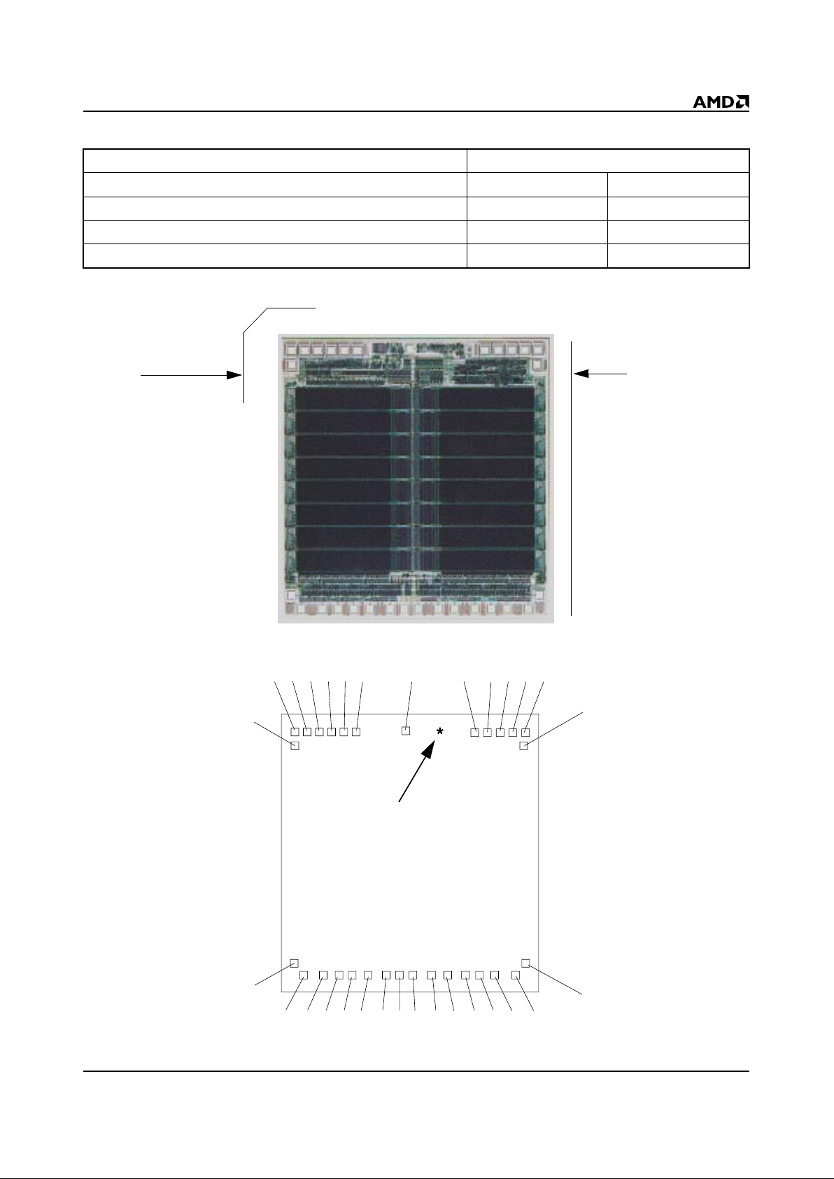
PRODUCT SELECTOR GUIDE
DIE PHOTOGRAPH
DIE PAD LOCATIONS
Family Part Number Am29F010 KGD
Speed Option (V
CC
= 5.0 V ± 10%) -90 -120
Max Access Time, t
ACC
(ns) 90 120
Max CE# Access, t
CE
(ns) 90 120
Max OE# Access, t
OE
(ns) 35 50
Orientation relative to
top left corner of
Gel-Pak
Orientation relative to
leading edge of tape
and reel
1234567
8
9
10 11 12 13 14 15 16 17 18 19 20 21 22 23
24
25
2627282930
AMD logo location
Page 4

4 Am29F010 Known Good Die 1/13/98
SUPPLEMENT
PAD DESCRIPTION
Note: The coordinates above are relative to the center of pad 1 and can be used to operate wire bonding equipment.
Pad Signal
Pad Center (mils) Pad Center (millimeters)
XYXY
1V
CC
0.00 0.00 0.00 0.00
2 A16 –33.20 –1.30 –0.84 –0.03
3 A15 –41.60 –1.30 –1.06 –0.03
4 A12 –49.90 –1.30 –1.27 –0.03
5 A7 –58.30 –1.30 –1.48 –0.03
6 A6 –66.60 –1.30 –1.69 –0.03
7 A5 –75.00 –1.30 –1.91 –0.03
8 A4 –74.40 –10.50 –1.89 –0.27
9 A3 –75.60 –158.20 –1.92 –4.02
10 A2 –69.40 –166.80 –1.76 –4.24
11 A1 –56.10 –166.80 –1.42 –4.24
12 A0 –46.10 –166.80 –1.17 –4.24
13 D0 –36.30 –166.90 –0.92 –4.24
14 D1 –25.90 –166.90 –0.66 –4.24
15 D2 –13.30 –166.90 –0.34 –4.24
16 V
SS
–4.30 –166.90 –0.11 –4.24
17 D3 4.70 –166.90 0.12 –4.24
18 D4 17.30 –166.90 0.44 –4.24
19 D5 27.60 –166.90 0.70 –4.24
20 D6 40.20 –166.90 1.02 –4.24
21 D7 50.60 –166.90 1.29 –4.24
22 CE# 60.60 –166.80 1.54 –4.24
23 A10 74.00 –166.80 1.88 –4.24
24 OE# 81.40 –158.20 2.07 –4.02
25 A11 80.20 –10.40 2.04 –0.26
26 A9 80.80 –1.30 2.05 –0.03
27 A8 72.40 –1.30 1.84 –0.03
28 A13 64.10 –1.30 1.63 –0.03
29 A14 55.70 –1.30 1.41 –0.03
30 WE# 47.40 –1.30 1.20 –0.03
Page 5

1/13/98 Am29F010 Known Good Die 5
SUPPLEMENT
ORDERING INFORMATION
Standard Products
AMD KGD produ cts ar e avai lable i n seve ral pa ckages and operat ing ranges. T he or der nu mber (Valid Combin ation) is form ed
by a combination of the following:
Valid Combinations
Valid Combinations list configurations planned to be supported in volume for this device. Consult the local AMD sales
office to confirm availability of specific valid combinations and
to check on newly released combinations.
Am29F010
DEVICE NUMBER/DESCRIPTION
Am29F010 Known Good Die
1 Megabit (128 K x 8-Bit) CMOS Flash Memory—Die Revision 1
5.0 Volt-only Program and Erase
-90
SPEED OPTION
See Valid Combinations
PACKAGE TYPE AND MINIMUM ORDER QUANTITY
DP = Waffle Pack
245 die per 5 tray stack
DG = Gel-Pak
®
Die Tray
486 die per 6 tray stack
DT = Surftape™ (Tape and Reel)
2500 per 7-inch reel
DW = Gel-Pak
®
Wafer Tray (sawn wafer on frame)
Call AMD sales office for minimum order quantity
TEMPERATURE RANGE
C = Commercial (0°C to +70°C)
I=Industrial (–40°C to +85°C)
E = Extended (–55°C to +125°C)
DP
C
1
DIE REVISION
This number refers to the specific AMD manufacturing
process and product technology reflected in this
document. It is entered in the revision field of AMD
standard product nomenclature.
Valid Combinations
Am29F010-90 DPC 1, DPI 1, DPE 1,
DGC 1, DGI 1, DGE 1,
DTC 1, DTI 1, DTE 1,
DWC 1, DWI 1, DWE 1
Am29F010-120
Page 6

6 Am29F010 Known Good Die 1/13/98
SUPPLEMENT
PRODUCT TEST FLOW
Figure 1 pr ovi d es an overview of AMD ’s K n own Good
Die test flow. For more detailed information, refer to the
Am29F010 product qualification database supplement
for KGD. AMD implements quality assurance procedures th roug hout t he pro duct t est flow. In addi tion, an
off-line quality monitoring program (QMP) further guarantees AMD quality standards are met on Known Good
Die products. These QA procedures also allow AMD to
produce KGD products without requiring or implementing burn-in.
Figure 1. AMD KGD Product Test Flow
Wafer So rt 1
Bake
24 hours at 250°C
Wafer Sort 2
Wafer So rt 3
High Temperature
Packaging for Shipment
Shipment
DC Parameters
Functionality
Programmability
Erasability
Data Retention
DC Parameters
Functionality
Programmability
Erasability
DC Parameters
Functionality
Programmability
Erasability
Speed
Incoming Inspection
Wafer Saw
Die Separation
100% Visual Inspection
Die Pack
Page 7

1/13/98 Am29F010 Known Good Die 7
SUPPLEMENT
PHYSICAL SPECIFICATIONS
Die dimensions . . . . . . . . . . . . . . 174 mils x 189 mils
4.42 mm x 4.80 mm
Die Thickness . . . . . . . . . . . . . ~20 mils or ~0.51 mm
Bond Pad Size . . . . . . . . . . . . . . 4.47 mils x 4.47 mils
113.48 µm x 113.48 µm
Pad Area Free of Passivation . . . . . . . . . .19.98 mils
2
12,878 µm
2
Pads Per Die . . . . . . . . . . . . . . . . . . . . . . . . . . . . . .30
Bond Pad Metalization. . . . . . . . . . . . . . . . . . Al/Si/Cu
Die Backside . . . . . . . . . . . . . . . . . . . . . . . . No metal,
may be grounded (optional)
Passivation. . . . . . . . . . . . . . . . . . Nitride/SOG/Nitride
DC OPERATING CONDITIONS
VCC (Supply Voltage) . . . . . . . . . . . . . . .4.5 V to 5.5 V
Junction Temperature Under Bias . .T
J
(max) = 130°C
For Read-only . . . . . . . . . . .T
J
(max) = 140°C
Operating Temperature . . . Commercial 0°C to +70°C
Industrial –40°C to +85°C
Extended –5 5 ° C to +125°C
MANUFACTURING INFORMATION
Manufacturing and Test. . . . . . . . . Fab 14, Austin, TX
Manufacturing ID. . . . . . . . . . . . . . . . . . . . . .98108AK
Preparation for Shipment . . . . . . . . Penang, Malaysia
Fabrication Process . . . . . . . . . . . . . . . . . CS19AFDS
Die Revision . . . . . . . . . . . . . . . . . . . . . . . . . . . . . . . 1
SPECIAL HANDLING INSTRUCTIONS
Processing
Do not expose KGD products to ultraviolet light or
proce ss them at temperat ures greater tha n 250°C.
Failure to adher e to these handling ins tructions will
result in irreparable damage to the devices. For best
yiel d, AMD recom mends assem bly in a Clas s 10K
clean room with 30% t o 60% relative humidity.
Storage
Store at a maximum temperature of 30°C in a nitrogenpurged cabinet or vacuum-sealed bag. Observe all
standard ESD handling procedures.
Page 8

8 Am29F010 Known Good Die 1/13/98
SUPPLEMENT
TERMS AND CONDITIONS OF SALE FOR
AMD NON-VOLATILE MEMORY DIE
All transactions relating to AMD Products under this
agreement shall be subject to AMD’s standard terms
and co nd iti on s o f s ale , o r an y r evisions t her eo f, whi c h
revisio ns AMD res erves the rig ht to make at an y time
and from ti m e t o tim e . In th e e ve nt o f conflict bet wee n
the provisions of AMD’s standard terms and conditions
of sale and this agreement, the terms of this agreement
shall be controlling.
AMD warrants artic les of its manufacture against
defective materials or workmanship for a period of
ninety (9 0) da ys fr om d ate of ship ment. This warr anty
does not extend beyond AMD’s customer, and does
not extend to die which has been affixed onto a board
or substrate of any kind. The liability of AMD under this
warranty is limited, at AMD’s option, solely to repair or
to repla cemen t wit h equiv ale nt artic les, or to m ake a n
appropriate credit adjustment not to exceed the original
sales price, for articles returned to AMD, provided that:
(a) The Buyer promptly notifies AMD in writing of each
and every defect or nonco nformity in any article for
which Buy er w ishe s to mak e a wa rran ty claim again st
AMD; (b) Buyer obtains authorizatio n from AMD to
return the ar ticle; (c) the articl e is returned to AMD,
trans por tati on c har ges paid by AMD, F.O.B. AMD ’s fa ctory; and (d) AMD’s examination of such article discloses to its satisfaction that such alleged d efect or
nonconformity actually exists and was not caused by
negligence, misuse, improper installation, accident or
unauthorized repair or alteration by an entity other than
AMD. The afore mentioned provisions do not extend
the original warranty period of any article whi ch has
either been repaired or replaced by AMD.
THIS WARRANTY IS EXPRESSED IN LI EU OF ALL
OTHER WARR ANTIES, EXPR ESSED OR IMPLIED,
INCLUDING THE IMPLIED WARRANTY OF FI TNESS
FOR A PARTICULAR PURPOSE, THE IMPLI ED
WARRANTY OF MERCHANTABILITY AND OF ALL
OTHER OBLIGATIONS OR LIABILITIES ON AMD’S
PART, AND IT NEITHER ASSUMES NOR AUTHORIZES ANY OTHER PERSON TO ASSUME FOR
AMD ANY OTHER LIABILITIES. THE FOR EGOING
CONSTITUTES THE BUYERS SOLE AND EXCL USIVE REMEDY FOR THE FURNISHING OF DEFECTIVE OR NON CONFORMING ARTICLES AND AMD
SHALL NOT IN ANY EVENT BE LIABLE FOR
DAMAGES BY REASON OF FAILURE OF ANY
PRODUCT TO FUNCTION PROPERLY OR FOR ANY
SPECIAL, INDIRECT, CONSEQUENTIAL, INCIDENTAL OR EXEMPLARY DAMAGES, INCLUDING
BUT NOT LIMITED TO, LOSS OF PROFITS, LOSS
OF USE OR COST OF LABOR BY REASON OF THE
FACT T HAT SUCH ARTICLES SHALL HAVE BEEN
DEFECTIVE OR NON CONFORMING.
Buyer agrees that it will make no warranty representations to its customer s which exceed those g iven by
AMD to Buyer unless and until Buyer shall agree to
indemnify AMD in wr iting for a ny claims w hich ex cee d
AMD’s warrant y. B uyer assumes all responsibil ity for
success ful die pr ep, di e attach and wire b ondin g processes. D ue to the unprotecte d nature o f the AMD
Products which are the subject hereof, AMD assumes
no responsibility for environmental effects on die.
AMD produ cts are not de signed or author ized for use
as components in life support appliances, devices or
systems where malfunction of a product can reasonably be expected to result in a personal injury. Buyer’s
use of A MD pro duct s for use i n li fe sup por t app lic ati ons
is at Buyer’s own risk and Buyer agrees to fully indemnify AMD for an y damages resu lting in such use o r
sale.
REVISION SUMMARY FOR AM29F010
KNOWN GOOD DIE
Formatted to match current template. Updated Distinctive Characteris tics and General Description sections
using the current main data sheet.
Trademarks
Copyright © 1998 Advanced Micro Devices, Inc. All rights reserved.
AMD, the AMD logo, and combinations thereof are registered trademarks of Advanced Micro Devices, Inc.
Product names used in this publication are for identification purposes only and may be trademarks of their respective companies.
 Loading...