

Page 1

查询AM186ED供应商
PRELIMINARY
Am186TMED/EDLV
High Performance, 80C186- and 80C188-Compatible,
16-Bit Embedded Microcontrollers
DISTINCTIVE CHARACTERISTICS
n E86TM family 80C186- and 80C188-compatible
microcontroller with enhanced bus interface
– Lower system cost with higher performance
– 3.3-V ± 0.3-V operation (Am186EDLV
microcontrollers)
n Programmable DRAM Controller
– Supports zero-wait-state operation with 50-ns
DRAM at 40 MHz, 60-ns @ 33 M Hz, 70- ns @ 25
MHz
– Includes programmable CAS
refresh capability
n High performance
– 20-, 25-, 33-, and 40-MHz operating frequencies
– Zero-wait-state operation at 40 MHz with 70-ns
static memory
– 1-Mbyte memory address space
– 64-Kbyte I/O space
n Enhanced features provide improved memory
access and remove the requirement for a 2x clock
input
– Nonmultiplexed address bus
– Processor operates at the clock input frequency
– 8-bit or 16-bi t program mable b us sizi ng includ ing
8-bit boot option
n Enhanced integrated peripherals
– 32 programmable I/O (PIO) pins
– Two full-featured asynchronou s seri al ports allo w
full-duplex, 7-bit, 8-bit, or 9-bit data transfers
-before-RAS
– Serial port hardware handshaking with CTS
RTS, ENRX, and RTR selectable for each port
– Improved serial port operation enhances 9-bit
DMA support
– Independent serial port baud rate generators
– DMA to and from the serial ports
– Watchdog timer can generate NMI or reset
– A pulse-width demodulation option
– A data strobe, tr ue asynchronous bus interfac e
option included for DEN
– Reset configuration register
n Familiar 80C186 peripherals
– Two independent DMA channels
– Programmable interrupt controller with up to 8 ex-
ternal and 8 internal interrupts
– Three programmable 16-bit timers
– Programmable memory and peripheral
chip-select logic
– Programmable wait state generator
– Power- save cl oc k div id er
n Software-compatible with the 80C186 and
80C188 microcontrollers with widely available
native development tools, applications, and
system software
n A compatible evolution of the Am186EM,
Am186ES, and Am186ER microcontrollers
n Available in the following packages:
– 100-pin, thin quad flat pack (TQFP)
– 100-pin, plastic quad flat pack (PQFP)
RA
,
FT
GENERAL DESCRIPTION
The Am186TMED/EDLV microcontrollers are part of the
AMD E86
croprocessors based on the x86 architecture. The
Am186ED/EDLV microcontrollers are the ideal upgrade
for 80C186/188 designs requiring 80C186/188 compatibility, increased performance, serial communications, a
direct bus interface, and more than 64K of memory.
The Am186ED/EDLV microcontrollers integrate a complete DRAM control ler to ta ke adv antage of low DRAM
costs. This reduces memory subsystem costs while
maintaining SRAM performance.The Am186ED/EDLV
microcontrollers a lso integrate t he functions of a CPU,
nonmultiplexed address bus, three timers, watchdog
timer, chip selects, interrupt controller, two DMA controllers, two asynchronous serial ports, programmable bus
This document contains information on a product under development at Advanced Micro Devices. The information
is intended to help you evaluate this pro duct. AMD reserves t he right to change or discontinue work o n this proposed
product without notice. AMD, the AMD logo, and combinations there of are tra dema rks of Adva nced Micr o Devices,
Inc.
TM
family of embedded mic roco ntrollers a nd mi-
D
sizing, and programmable I/O (PIO) pins on one chip.
Compared to the 80C186/188 microcontrollers, the
Am186ED/EDLV microcontrollers enable designers to
reduce the size, power consumption, and cost of embedded systems, whi le i nc reas in g r eli ab ili ty, functionality, and performance.
The Am186ED/EDLV microcontrollers have been
designed to meet the most common requirements of
embedded products developed for the communications,
office automation, mass storage, and general
embedded markets. Specific applications include
PBXs, multiplexers, modems, disk drives, hand-held
and desktop terminals, fax machines, printers,
photocopiers, and industrial controls.
Publication# 21336 Rev: A Amendment/0
Issue Date: May 1997
Page 2
PRELIMINARY
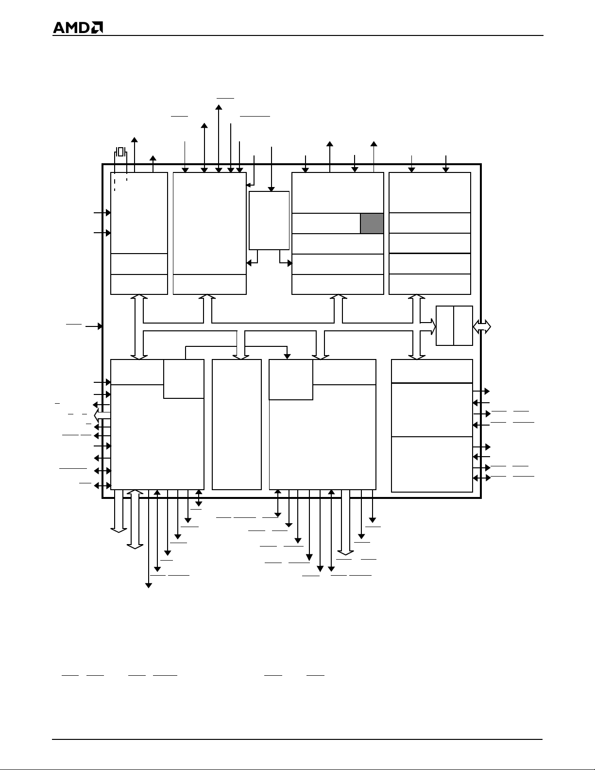
Am186ED/EDLV MICROCONTROLLERS BLOCK DIAGRAM
V
CC
GND
RES
ARDY
SRDY
S2/BTSEL
S1–S0
DT/R
DEN/DS
HOLD
HLDA
S6/CLKDIV2
UZI
INT3/INTA
CLKOUTA
CLKOUTB
X2
X1
Clock and
Power
Management
Unit
Watchdog
Timer (WDT)
Control
Registers
Control
Registers
Bus
Interface
Unit
1/IRQ
INT6–INT4**
Interrupt
Control Unit
Control
Registers
Refresh
Control
Unit
INT2/INTA
0/PWD**
INT1/SELECT
INT0
NMI
Demod-
Execution
Unit
PWD**
Pulse
Width
ulator
(PWD)
TMROUT0 TMROUT1
TMRIN0 TMRIN1
Timer Control
Unit
01 2 0 1
Max Count B
Registers
Max Count A
Registers
16-Bit Coun t
Registers
Control
Registers
DRAM
Control
Unit
Chip-Select
Control
Registers
Unit
DRQ0/INT5** DRQ1/INT6**
20-Bit Destination
FT
Asynchronous
Asynchronous
RA
DMA
Unit
20-Bit Source
Pointers
Pointers
16-Bit Coun t
Registers
Control
Registers
Control
Control
Registers
Serial Port 0
Serial Port 1
Unit
Registers
PIO
PIO31–
PIO0*
TXD0
RXD0
RTS0/RTR0
CTS0/ENRX0
TXD1
RXD1
RTS1/RTR1**
CTS1/ENRX1**
RD
WHB
A19–A0
D
AD15–AD0
Notes:
*All PIO signal s are shared with o the r physical pins. Se e th e pin de sc riptions beginning on page 21 and Table 2 on page 29 for
information on shared functions.
1/RTR1 and CTS1/ENRX1 are multiplexed with PCS3 and PCS2, respectively. See the pin descriptions beginning on
** RTS
page 21.
2 Am186ED/EDLV Microcontrollers
ALE
BHE
WLB
WR
/ADEN
LCS/ONCE0/RAS0
MCS3/RAS1
MCS
MCS1/UCAS
2/LCAS
MCS0
PCS
UCS
PCS6/A2
PCS
3–PCS0**
/ONCE1
5/A1
Page 3
PRELIMINARY
,
ORDERING INFORMATION
Standard Products
AMD standard products are available in s everal package s and operating ranges. The order num ber (valid combi nation) is formed
by a combination of the elements below.
-40 K C \WAm186TMED/EDLV
LEAD FORMING
\W=Trimmed and Formed
TEMPERAT URE RANGE
C= ED Commercial (T
C = EDLV Commercial (T
I = ED Industrial (T
where: TC= case temperature
where: T
PACKAGE TYPE
V=100-Pin Thin Quad Flat Pack (TQFP)
K=100-Pin Plastic Quad Flat Pack (PQFP)
SPEED OPTION
–20 = 20 MHz
–25 = 25 MHz
–33 = 33 MHz
–40 = 40 MHz
= ambient temperature
A
=0°C to +100°C)
C
=0°C to +70°C)
C
=–40°C to +85°C)
A
Valid Combinations
Am186ED–20
Am186ED–25
Am186ED–33
Am186ED–40
Am186ED–20
Am186ED–25
Am186EDLV–20
Am186EDLV–25
Note:
D
The industrial version of the Am186ED is
offered only in the PQFP package.
VC\W or
KC\W
RA
1
KI\W
VC\W or
KC\W
DEVICE NUMBER/DESCRIPTION
Am186ED = High-Performance, 80C186-Compatible,
16-Bit Embedded Microcontroller
Am186EDLV = High-Performance, 80L186-Compatible
Low-Voltage, 16-Bit Embedded Microcontroller
V alid combinations list c onfigurations planned to be
supported in volume for this device. Consult the
local AMD sales office to confirm availability of
specific valid combinations and to check on newly
released combinations.
Note: The industrial version of the Am186ED as
well as the Am186EDL V are available in 20 and 25
MHz operating frequencies only.
The Am186ED and Am186EDLV microcon trollers
are all functionally the same except for their DC
characteristics and available frequencies.
Note: There is no 188 version of the Am186ED/
EDLV. The same 8-bit external bus capabilities
can be achieved us ing the 8-bit bo ot capability and
programmable bus sizing options.
FT
Valid Combinations
Am186ED/EDLV Microcontrollers 3
Page 4
PRELIMINARY
TABLE OF CONTENTS
DISTINCTIVE CHARACTERISTICS ........................................................................................... 1
GENERAL DESCRIPTION .......................................................................................................... 1
AM186ED/EDLV MICROCONTROLLERS BLOCK DIAGRAM ................................................... 2
ORDERING INFORMATION ....................................................................................................... 3
Standard Products ........................................................................................................... 3
RELATED AMD PRODUCTS .............................................................................................. ........ 9
E86 Family Devices ...................................................................................................... 9
Related Documents . ........................... .. .. ............. ... .. ............. .. ... ............. .. .. .................. 10
Third-Party Development Support Products .................................................................. 10
Customer Serv i ce ...... ........................... .. .. .............. .. .. ........................... .. .. ............. .. ... .. 10
KEY FEATURES AND BENEFITS ............................. .. .. .. .................................. .. .. .. .. ............... 10
Application Co n s id e ra t io n s ........ .......................... ... .. ............. .. ... ............. .. .. ............. ... .. .11
COMPARING THE AM186ED/EDLV TO THE AM186ES/ESLV MICROCONTROLLERS ........ 12
Integrated DRAM Controller ........................................................................................... 12
Enhanced Refresh Control Unit ..................................................................................... 13
Option to Overlap DRAM with PCS
Additional Serial Port Mode for DMA Support of 9-bit Protocols .................................... 13
Option to Boot from 8- or 16-bit Memory ....................................................................... 13
Improved External Bus Master Support ......................................................................... 13
PSRAM Controller Removed ......................................................................................... 13
TQFP CONNECTION DIAGRAMS AND PINOUTS .................................................................. 14
Top Side View—100-Pin Thin Quad Flat Pack (TQFP) .............................. .. .. ............... 14
TQFP PIN DESIGNATIONS ....................................................................................................... 15
Sorted by Pin Number .................................................................................................... 15
Sorted by Pin Name ....................................................................................................... 16
PQFP CONNECTION DIAGRAMS AND PINOUTS .................................................................. 17
Top Side View—100-Pin Plastic Quad Flat Pack (PQFP) .............................................17
PQFP PIN DESIGNATIONS................................................................................ .. .. .. .. ............... 18
Sorted by Pin Number .................................................................................................... 18
Sorted by Pin Name ....................................................................................................... 19
LOGIC SYMBOL—AM186ED/EDLV MICROCONTROLLERS ................................................. 20
PIN DESCRIPTIONS ................................................................................................................. 21
Pins That Are Used by Emulators .................................................................................. 21
Pin Terminology ............................................................................................................. 21
A19–A0 (A19/PIO9, A18/PIO8, A17/PIO7) .................................................................... 21
AD15–AD8 ..................................................................................................................... 21
AD7–AD0 ....................................................................................................................... 21
ALE ................................................................................................................................ 21
ARDY ............................................................................................................................. 22
D
/ADEN ...... ......... ....... ......... ......... ...... ......... ......... ......... ...... ......... ......... ......... ...... ..... 22
BHE
CLKOUTA ...................................................................................................................... 22
CLKOUTB ...................................................................................................................... 22
0/ENRX0/PIO21 ..... ........... ........... ......... ........... ........... ......... ........... ........... ........... .. 2 2
CTS
/DS/PIO5 ................................................................................................................ 23
DEN
DRQ0/INT5/PIO12 ......................................................................................................... 23
DRQ1/INT6/PIO13 ......................................................................................................... 23
/PIO4 ..................................................................................................................... 23
DT/R
GND ............................................................................................................................... 23
HLDA ............................................................................................................................. 23
HOLD ............................................................................................................................. 23
INT0 ............................................................................................................................... 24
INT1/SELECT
................................................................................................................ 24
RA
............................................................................... 13
FT
4 Am186ED/EDLV Microcontrollers
Page 5
PRELIMINARY
INT2/INTA0/PWD/PIO31 ... ............. .............. ............. ........... ............. ............. .............. .. 24
INT3/INTA
INT4/PIO30 .................................................................................................................... 25
LCS
MCS
MCS
MCS2
MCS3
NMI ................................................................................................................................ 26
PCS
PCS
PCS
PCS
PCS
PIO31–PIO0 (Shared) ............................................................................... .. .. .. ............... 28
............. .................... .................... ................. .................... .................... .................. .. 28
RD
RES
RTS
RXD0/PIO23 .................................................................................................................. 30
RXD1/PIO28 .................................................................................................................. 30
2/BTSEL ...................................................................................................................... 30
S
1–S0 ............................................................................................................................ 30
S
S6/CLKDIV
SRDY/PIO6 .................................................................................................................... 30
TMRIN0/PIO 11 ........... .............. ............. ........... ............. .............. ............. ........... ........... 31
TMRIN1/PIO0 ................................................................................................................ 31
TMROUT0/PIO10 .......................................................................................................... 31
TMROUT1/PIO1 ............................................................................................................ 31
TXD0/PIO22 ......... ......... ........ ....... ......... ......... ......... ...... ......... ......... ....... ........ ......... ....... 31
TXD1/PIO27 ......... ......... ........ ....... ......... ......... ......... ...... ......... ......... ....... ........ ......... ....... 31
UCS
/PIO26 ...................................................................................................................... 31
UZI
................................................................................................................................ 31
V
CC
WHB
WLB
................................................................................................................................. 32
WR
X1 ......... ....... .... ....... ....... ...... ..... ...... ....... .... ....... ....... ...... ..... ...... ....... ....... .... ....... ...... ..... .. 32
X2 ......... ....... .... ....... ....... ...... ..... ...... ....... .... ....... ....... ...... ..... ...... ....... ....... .... ....... ...... ..... .. 32
FUNCTIONAL DESCRIPTION ..................................... ............................................... .............. 33
Memory Organization ..................................................................................................... 33
I/O Space ....................................................................................................................... 33
BUS OPERATION ...................................................... ...... .........................................................34
BUS INTERFACE UNIT ............................... .. ........................ .. ............................................... ... 36
Nonmultiplexed Address Bus ......................................................................................... 36
DRAM Address Multiplexing .......................................................................................... 36
Programmable Bus Sizing ............................................................................................. 37
Byte-Write Enables ........................................................................................................ 37
Data Strobe Bus Interface Option .................................................................................. 37
DRAM INTERFACE ................................................................................................................... 37
PERIPHERAL CONTROL BLOCK ............................... .. .. .................................. .. .. .. .. ............... 38
Reading and Writing the PCB .................................. .. .. .. .. .................................. .. .. .. .. .... 38
1/IRQ ....... ......................... ...................... ........................ ........................ ....... 24
/ONCE0/RAS0 ........................................................................................................ 25
0/PIO14 ...... ................. .................... .................... .................... .................. ............. 25
1/UCAS/PIO15 ... .................... .................... .................. .................... .................... .. 25
/LCAS/PIO24 ....................................................................................................... 25
/RAS1/PIO25 ....................................................................................................... 26
1/PIO17, PCS0/PIO16 ........ .................... ................. .................... .................... ....... 26
2/CTS1/ENRX1/PIO18 ........................................................................................... 27
3/RTS1/RTR1/PIO19 ............ ................................................................ .................. 27
5/A1/PIO3 ............................................................................................................... 27
6/A2/PIO2 ............................................................................................................... 28
............. ......... ......... ...... ......... ......... ....... ........ ......... ......... ....... ......... ........ ......... ....... 28
0/RTR0/PIO20 ........................................................................................................ 30
2/PIO29 ....................................................................................................... 30
FT
/ONCE1 .................................................................................................................. 31
............ ......... ......... ...... ......... ......... ....... ........ ......... ......... ....... ......... ........ ......... ....... 31
............................................................................................................................... 32
RA
D
Am186ED/EDLV Microcontrollers 5
Page 6

PRELIMINARY
CLOCK AND POWER MANAGEMENT .................................................................................... 40
Phase-Locked Loop ...................................... ................................................................. 40
Crystal-Driven Clock Source .......................................................................................... 40
External Source Clock ................................................................................................... 41
System Clocks ............................................................................................................... 41
Power-Save Op e ra t io n ........ .............. .. .. .......................... ... .. ............. .. ... ............. .. .. ....... 4 1
Initialization and Processor Reset ................. .. ........................ .. ....................... .............. 41
Reset Configuration Register ......................................................................................... 41
CHIP-SELECT UNIT .................................................................................................................. 42
Chip-Select Timing ......................................................................................................... 42
Ready and Wait-State Programming ............................................................................. 42
Chip-Select Overlap ....................................................................................................... 42
Upper Memory Chip Select ............................................................................................ 43
Low Memory Chip Select ............................................................................................... 43
Midrange Memory Chip Selects ..................................................................................... 43
Peripheral Chip Selects ....................... ....................................................................... ... 43
REFRESH CONTROL UNIT ...................................................................................................... 44
INTERRUPT CONTROL UNIT ............. .. ............................................... .................................... 44
TIMER CONTROL UNIT ............................................................................................................ 45
Watchdog Timer ............................................................................................................. 45
PULSE WIDTH DEMODULATION ............................................................................................ 45
DIRECT MEMORY ACCESS .................................................................................................... 46
DMA Operation ...... .. .. .............. .. .. ............. ... .. ............. .. .. ........................... .. .. .............. .. 46
DMA Channel Control Registers ....................................................................................47
DMA Priority ........................ .. ... ............. .. .. ........................... .. .. .............. .. .. ............. .. ... .. 47
ASYNCHRONOUS SERIAL PORTS ............................................ .. ...... ..................................... 47
DMA Transfers through the Serial Port ............... ....................... .................................... 48
PROGRAMMABLE I/O (PIO) PINS ........................................................................................... 48
ABSOLUTE MAXIMUM RATINGS ............................................................................................ 49
OPERATING RANGES ............................... .. ............................................................................ 49
DC CHARACTERISTICS OVER COMMERCIAL AND INDUSTRIAL OPERATING RANGES . 49
CAPACITANCE ......................................................................................................................... 50
POWER SUPPLY CURRENT ............................................................... ...... .............................. 50
THERMAL CHARACTERISTICS ............................................................................................... 51
TQFP Package ................................................. .. .. .................................. .. .. .. .. ............... 51
Typical Ambient Temperatures....................................................................................... 52
COMMERCIAL AND INDUSTRIAL SWITCHING CHARACTERISTICS AND WAVEFORMS .. 57
Key to Switchin g Wa v e fo r m s ..... .. .. .............. .. .. ........................... .. .. ............. .. ... ............. 57
Alphabetical Key to Switching Parameter Symbols ....................................................... 58
Numerical Key to Switching Parameter Symbols ........................................................... 61
SWITCHING CHARACTERISTICS OVER COMMERCIAL AND INDUSTRIAL
SWITCHING CHARACTERISTICS OVER COMMERCIAL OPERATING RANGES ................. 65
READ CYCLE WAVEFORMS ................................................................................................... 66
SWITCHING CHARACTERISTICS OVER COMMERCIAL AND INDUSTRIAL
SWITCHING CHARACTERISTICS OVER COMMERCIAL OPERATING RANGES ................. 68
WRITE CYCLE WAVEFORMS ..................................... ............................................... .............. 69
D
OPERATING RANGES ............................................................................................... 64
Read Cycle (20 MHz and 25 MHz) ................................................................................ 64
Read Cycle (33 MHz and 40 MHz) ................................................................................ 65
OPERATING RANGES ............................................................................................... 67
Write Cycle (20 MHz and 25 MHz) ................................................................................67
Write Cycle (33 MHz and 40 MHz) ................................................................................68
RA
FT
6 Am186ED/EDLV Microcontrollers
Page 7

PRELIMINARY
SWITCHING CHARACTERISTICS OVER COMMERCIAL AND INDUSTRIAL
OPERATING RANGES ............................................................................................... 70
DRAM ............................................................................................................................ 70
DRAM Read Cycle Timing with No-Wait States ............................................................ 71
DRAM Read Cycle Timing with Wait State(s) ................................................................ 71
DRAM Write Cycle Timing with No-Wait States ............................................................. 72
DRAM Write Cycle Timing With Wait State(s) ............................................................... 72
DRAM CAS
SWITCHING CHARACTERISTICS OVER COMMERCIAL AND INDUSTRIAL
OPERATING RANGES ............................................................................................... 74
Interrupt Acknowledge Cycle (20 MHz and 25 MHz) ....................................... .............. 74
SWITCHING CHARACTERISTICS OVER COMMERCIAL OPERATING RANGES ................. 75
Interrupt Acknowledge Cycle (33 MHz and 40 MHz) ....................................... .............. 75
INTERRUPT ACKNOWLEDGE CYCLE WAVEFORMS ........................................................... 76
SWITCHING CHARACTERISTICS OVER COMMERCIAL AND INDUSTRIAL
OPERATING RANGES ............................................................................................... 77
Software Halt Cycle (20 MHz and 25 MHz) ................................................................... 77
SWITCHING CHARACTERISTICS OVER COMMERCIAL OPERATING RANGES ................. 77
Software Halt Cycle (33 MHz and 40 MHz) ................................................................... 77
SOFTWARE HALT CYCLE WAVEFORMS .............................................................................. .78
SWITCHING CHARACTERISTICS OVER COMMERCIAL AND INDUSTRIAL
OPERATING RANGES ............................................................................................... 79
Clock (20 MHz and 25 MHz) .......................................................................................... 79
SWITCHING CHARACTERISTICS OVER COMMERCIAL OPERATING RANGES ................. 80
Clock (33 MHz and 40 MHz) .......................................................................................... 80
CLOCK WAVEFORMS .............................................................................................................. 81
Clock Waveforms—Active Mode ................................................................................... 81
Clock Waveforms—Power-Save Mode .......................... ....................... .........................81
SWITCHING CHARACTERISTICS OVER COMMERCIAL AND INDUSTRIAL
OPERATING RANGES ............................................................................................... 82
Ready and Peripheral (20 MHz and 25 MHz) ................................................................ 82
SWITCHING CHARACTERISTICS OVER COMMERCIAL OPERATING RANGES ................. 82
Ready and Peripheral (33 MHz and 40 MHz) ................................................................ 82
SYNCHRONOUS, ASYNCHRONOUS, AND PERIPHERAL WAVEFORMS ............................ 83
Synchronous Ready Waveforms ................................................................................... 83
Asynchronous Ready Waveforms ................................................ .................................. 83
Peripheral Waveforms ....................... ............................................................................ 83
SWITCHING CHARACTERISTICS OVER COMMERCIAL AND INDUSTRIAL
OPERATING RANGES ............................................................................................... 84
Reset and Bus Hold (20 MHz and 25 MHz) ............................ ....................................... 84
SWITCHING CHARACTERISTICS OVER COMMERCIAL OPERATING RANGES ................ 84
RESET AND BUS HOLD WAVEFORMS ...................................... .. .. .. .. .................................. .. .85
TQFP PHYSICAL DIMENSIONS ............................................................................................... 87
PQFP PHYSICAL DIMENSIONS ..................................................... .. .. .................................... .88
D
Reset and Bus Hold (33 MHz and 40 MHz) ............................ ....................................... 84
Reset Waveforms .......................................................................................................... 85
Signals Related to Reset Waveforms .............................. ....................... .......................85
Bus Hold Wavefo rms—Entering .... ... ............. .. .. ............. ... .. .......................... ... .. ........... 86
Bus Hold Waveforms—Leaving ..................................................................................... 86
-before-RAS Cycle Timing .......................................................................... 73
FT
RA
Am186ED/EDLV Microcontrollers 7
Page 8

PRELIMINARY
LIST OF FIGURES
Figure 1 Am186ED Microcontroller Example System Design .............................................. 11
Figure 2 80C186 Microcontroller Example System Design ................................................. 12
Figure 3 Two-Component Address ......................................................................................33
Figure 4 16-Bit Mode—Normal Read and Write Operation ................................................. 34
Figure 5 16-Bit Mode—Read and Write with Address Bus Disable In Effect ....................... 35
Figure 6 8-Bit Mode—Normal Read and Write Operation ................................................... 35
Figure 7 8-Bit Mode—Read and Write with Address Bus Disable in Effect ......................... 36
Figure 8 Am186ED/EDLV Microcontrollers Oscillator Configurations ................................. 40
Figure 9 Clock Organization ................................................................................................ 41
Figure 10 DMA Unit Block Diagram ....................................................................................... 47
Figure 11 Typical I
Figure 12 Typical I
Figure 13 Thermal Resistance(°C/Wat t) ......... ........... ......... ........... ........... ........... ......... ......... 51
Figure 14 Thermal Character is tics Equations .............. ........................... .. .. .............. .. .. ......... 51
Figure 15 Typical Ambient Temperatures for PQFP with a 2-Layer Board ............................ 53
Figure 16 Typical Ambient Temperatures for TQFP with a 2-Layer Board ............................ 54
Figure 17 Typical Ambient Temperatures for PQFP with a 4-Layer to 6-Layer Board ..........55
Figure 18 Typical Ambient Temperatures for TQFP with a 4-Layer to 6-Layer Board ........... 56
LIST OF TABLES
Versus Frequency for Am186EDLV Microcontroller .............................50
cc
Versus Frequency for Am186ED Microcontroller ................................. 50
cc
Table 1 Data Byte Encoding ............................................................................................... 22
Table 2 Numeric PIO Pin Designations ............................ ............................................... ... 29
Table 3 Alphabetic PIO Pin Designations ........................................................................... 29
Table 4 Bus Cycle Encoding ............................................................................................... 30
Table 5 Segment Register Selection Rules ........................................................................ 33
Table 6 DRAM Pin Interface ................................ .. .. .. .................................. .. .. .. .. ............... 37
Table 7 Programming the Bus Width of Am186ED/EDLV Microcontrollers ........................ 37
Table 8 Peripheral Control Block Register Map ........................................... .......................39
Table 9 Am186ED/EDLV Microcontrollers Maximum DMA Transfer Rates ....................... 46
Table 10 Typical Power Consumption Calculation fo r the Am186EDLV Microcontroller ...... 50
Table 11 Thermal Characteristics (°C/Watt) ......................................................................... 51
Table 12 Typical Power Consumption Calculation ............................................................... 52
Table 13 Junction Temperature Calculation ......................................................................... 52
Table 14 Typical Ambient Temperatures (°C) for PQFP with a 2-Layer Board .................... 53
Table 15 Typical Ambient Temperatures (°C) for TQFP with a 2-Layer Board .................... 54
Table 16 Typical Ambient Temperatures (°C) for PQFP with a 4-Layer to 6-Layer Board ... 55
Table 17 Typical Ambient Temperatures (°C) for TQFP with a 4-Layer to 6-Layer Board ... 56
RA
FT
D
8 Am186ED/EDLV Microcontrollers
Page 9
PRELIMINARY
Microprocessors
AT Peripheral
Microcontrollers
186 Peripheral
Microcontrollers
Am386SX/DX
Microprocessors
ÉlanSC300
Microcontroller
80C186 and 80C188
Microcontrollers
80L186 and 80L188
Microcontrollers
The E86 Family of Embedded Microprocessors and Microcontrollers
Am486DX
Microprocessor
ÉlanSC310
Microcontroller
Am186EM and
Am188EM
Microcontrollers
Am186EMLV &
Am188EMLV
Microcontrollers
™
K86
Future
ÉlanSC400
Microcontroller
Am186ES and
Am188ES
Microcontrollers
Am186ESLV &
Am188ESLV
Microcontrollers
Time
ÉlanSC410
Microcontroller
Am186ER and
Am188ER
Microcontrollers
Microcontroller
Am486
Future
Am186ED
32-bit Future
Am186 and
Am188 Future
RELATED AMD PRODUCTS
E86 Family Devices
Device Description
80C186 16-bit microcontroller
80C188 16-bit microcontroller with 8-bit external data bus
80L186 Low-voltage, 16-bit microcontroller
80L188 Low-voltage, 16-bit microcontroller with 8-bit external data bus
Am186EM High-performance, 80C186-compatible, 16-bit embedded microcontroller
Am188EM High-performance, 80C188-compatible, 16-bit embedded microcontroller with 8-bit external data bus
Am186EMLV High-performance, 80C186-compatible, low-voltage, 16-bit embedded microcontroller
Am188EMLV High-performance, 80C188-compatible, low-voltage, 16-bit embedded microcontroller with 8-bit
Am186ES High-performance, 80C186-compatible, 16-bit embedded microcontroller
Am188ES High-performance, 80C188-compatible, 16-bit embedded microcontroller with 8-bit external data bus
Am186ESLV High-performance, 80C186-compatible, low-voltage, 16-bit embedded microcontroller
Am188ESLV High-performance, 80C188-compatible, low-voltage, 16-bit embedded microcontroller with 8-bit
Am186ED High-performance, 80C186- and 80C188-compatible, 16-bit embedded microcontroller with 8- or 16Am186EDLV High-performance, 80C186- and 80C188-compatible, low-voltage, 16-bit embedded microcontroller
Am186ER High-performance, 80C186-compatible, low-voltage, 16-bit embedded microcontroller with 32 Kbyte
Am188ER High-performance, 80C188-compatible, low-voltage, 16-bit embedded microcontroller with 8-bit
™
Élan
SC300 High-performance, highly integrated, low-voltage, 32-bit embedded microcontroller
ÉlanSC310 High-performance, single-chip, 32-bit embedded PC/AT microcontroller
ÉlanSC400 Single-chip, low-power, PC/AT-compatible microcontroller
ÉlanSC410 Single-chip, PC/AT- compatible microcontroller
Am386®DX High-performance, 32-bit embedded microprocessor with 32-bit external data bus
Am386®SX High-performance, 32-bit embedded microprocessor with 16-bit external data bus
Am486®DX High-performance, 32-bit embedded microprocessor with 32-bit external data bus
external data bus
RA
external data bus
D
bit external data bus
with 8- or 16-bit external data bus
of internal RAM
external data bus and 32 Kbyte of internal RAM
FT
Am186ED/EDLV Microcontrollers 9
Page 10

PRELIMINARY
Related Documents
The following documents provide additional
information regarding the Am186ED/EDLV
microcontrollers:
n
Am186ED/EDLV Microcontrollers User’s Manual
order # 21335
n
Am186 and Am188 Family Ins truction Set Manu al
order # 21267
n
FusionE86SM Catalog
n
E86 Family Support Tools Brief
n FusionE86 Development Tools Reference CD,
order # 21058
Third-Party Development
Support Products
The FusionE86SM Program of Partnerships for
Application Solutions prov ides the custo mer with an
array of products designed to meet critical time-tomarket needs. Products and solutions available from
the AMD FusionE86 partners include emulators,
hardware and software debuggers, board-level
products, and software development tools, among
others.
, order # 19255
, order # 20071
To download documents and software, ftp to
ftp.amd.com and log on as anonymous using your
E-mail address as a passw ord. Or via your web
browser, go to ftp://ftp.amd.com.
Questions, reques ts, and input concerning AM D’s
,
WWW pages can be sent via E-mail to
webmaster@amd.com.
,
Documentation and Literature
Free E86 family information such as data books, user’s
manuals, data sheets, application notes, the
FusionE86 Partner Solutions Catalog, and other literature is available with a s imple phone call. Intern ationally, contact your local AMD sales office for complete
E86 family literature.
Literature Ordering
(800) 222-9323 Toll-free for U.S. and Canada
(512) 602-5651 Direct dial worldwide
(512) 602-7639 fax
(800) 222-9323 AMD Facts-On-Demand™
fax information service, tollfree for U.S. and Canada
In addition, mature development tools and applications
for the x86 platform are widely available in the general
marketplace.
Customer Service
The AMD customer service network includes U.S.
offices, international offices, and a customer training
center. Expert technical assista nce is available from
the worldwide staff of AMD field application engineers
and factory support staff to answer E86 family
hardware and software development questions.
Hotline and World Wide Web Support
For answers to technical questions, AMD provides a
toll-free number for direct access to our corporate
applications hotline. Also available is the AMD World
Wide Web home page and FTP site, which provides the
latest E86 family product info rmation, including
technical informati on and data on upcoming product
releases.
For technical support questions on all E86 products, send E-mail to lpd.support@amd.com.
Corporate Applications Hotline
(800) 222-9323 Toll-free for U.S. and Canada
44-(0) 1276-803-299 U.K. and Europe hotline
World Wide Web Home Page and FTP Site
To access the AMD home page go to:
http://www.amd.com.
D
RA
KEY FEATURES AND BENEFITS
The Am186ED/EDLV microcontrollers extend the AMD
family of microcon trollers based on the indus try-standard x86 architecture. The Am186ED/EDLV microcontrollers are a higher-perfo rmance, highly integrated
version of the 80C186/188 microprocessors, offering
an attractive migration path. In addition, the Am186ED/
EDLV microcontrollers offer application-specific features that can enhance t he system functi onality of the
Am186ES/ESLV and Am188ES/ESLV microcontrollers. Upgrading to the Am186ED/EDLV microcontrollers is an attractive solution for several reasons:
n Programmable DRAM controller—Enables sys-
tem designers to take advantage of low-cost DRAM
and fully utilize the performance and flexibility of the
x86 architecture. The DRAM controller supports
zero wait-state performance with 50-ns DRAM at 40
MHz, or, if required, can be programm ed with wait
states. The Am186ED/EDLV microcontrollers provide a CAS
n Minimized total syst em cost—New and en-
hanced peripherals and on-chip system interface
logic on the Am 186ED/EDLV microcontrollers r educe the cost of existing 80C186/188 designs.
n X86 software compatibility—80C186/188-com-
patible and upward-compatible with the other members of the AMD E86 family.
FT
-before-RAS refresh unit.
10 Am186ED/EDLV Microcontrollers
Page 11
PRELIMINARY
n Enhanced performance—The Am186ED/EDLV
microcontrollers increase the perform ance of
80C186/188 systems, and the nonmultiplexed address bus offers unbuffered access to memory.
n Enhanced functionality—The enhanced on-chip
peripherals of the Am186ED/EDLV microcontrollers
include two asynchronous serial ports, 32 PIOs, a
watchdog timer, additional interrupt pins, a pulse
width demodulation option, DMA directly to and from
the serial ports, 8-bit and 16-bit p rogrammable bus
sizing, a 16-bit reset configuration register, and enhanced chip-select functionality.
Application Considerations
The integration enhance men ts of the Am186ED/EDLV
microcontrollers provide a high-perfor mance, low- system-cost solution for 16-bit embedded mic rocontroller
designs. The nonmultiplexed address bus eliminates
the need for system-s upp or t l ogic to i nte rfa ce me mory
devices, while the multiplexed address/data bus maintains the value of previously engineered, customerspecific perip herals and circuits withi n the upgraded
design.
Figure 1 illust rates an example syst em design that
uses the integrated pe riphe ral s et to ac hi ev e high per formance with reduced system cost.
Clock Generation
The integrated clock generation circuitry of the
Am186ED/EDLV microcontrollers enables the use of a
1x crystal frequency. The Am186ED design in Figure 1
achieves 40-MHz CPU operation, while using a 40MHz crystal.
Memory Interface
The Am186ED/EDLV microcontrollers integrate a versatile memory controller which supports direct memory
accesses to DRA M, SR AM, Fl ash, EPROM, a nd R OM.
No external glue logic is requi re d and al l requi r ed co ntrol signals are provided. The peripheral chip selects
have been enhanced to allow them to overlap the
DRAM. This allows a sm all 1.5K portio n of the DRAM
memory space to be used for perip herals without b us
contention.
The improved memory timing specifications of the
Am186ED/EDLV microcontrollers allow for zero-waitstate operation at 40 MHz using 50-ns DRAM, 70-ns
SRAM, or 70-ns Flash memory. For 60-ns DRAM one
wait state is required at 40 MHz and zero wait states at
33 MHz and below. For 70-ns DRAM two wait states
are required at 40 MHz, one wait state at 33 MHz, and
zero wait states at 25 MHz and below. This reduces
overall system cost by enablin g the use of common ly
available memory speeds and taking advantage of
DRAM’s lower cost pe r bit over SRAM.
Figure 1 also shows a n implementation of an RS-232
console or modem communica tions port. Th e RS-232
to CMOS voltage-level converter is required for the
electrical interface with the external device.
D
RA
FT
Figure 1. Am186ED Microcontroller Example
System Design
Direct Memory Interface Example
Figure 1 illustrates the direct memory interface of the
Am186ED microcontroller. The processor’s A19–A0
bus connects to the mem ory address inputs, the AD
bus connects to the data inputs and outputs, and the
chip selects connect to the memory chip-select inputs.
The odd A1–A17 address pins connect to the DRAM
multiplexed address bus.
The RD
(OE
WR
pin. The UCAS
output connects to the DRAM Outpu t Enable
) pin for read oper ation s. Write op erations use th e
output connected to the DRAM Write Enable (WE)
and LCAS pins provide byte selection.
0-6
Am186ED/EDLV Microcontrollers 11
Page 12
PRELIMINARY
COMPARING THE Am186ES/ESLV TO THE Am186ED/EDLV MICROCONTROLLERS
Compared to the Am186ES/ESLV microcontrollers, the
Am186ED/EDLV microcontrollers have the following
additional features:
n Integrated DRAM controller
n Enhanced refresh control unit
n Option to overlap DRAM with peripheral chip select
(PCS)
n Additional serial port mode for DMA support of 9-bit
protocols
n Option to boot from 8- or 16-bit memory
n Improved external bus master support
n PSRAM controller removed
Figure 1 shows an examp le system using a 4 0-MHz
Am186ED microcontroller. Figure 2 shows a
comparable system implementation with an 80C186.
Because of its superior integration, the Am186ED/
EDLV system does not require the support devices that
are required on the 80C186 example system. In
addition, the Am186ED/EDLV microcontrollers provide
significantly bette r performance with its 4 0-MHz clock
rate.
Integrated DRAM Controller
The integrated DRAM controller directly interfaces
DRAM to support no-wait sta te DRAM interface up to
40 MHz. Wait states can be inser ted to support slower
DRAM. All signals required by the DRAM are
generated on the Am186ED/EDLV microcontrollers
and no external logic is required. The DRAM
multiplexed address p ins are connected to the odd
address pins startin g with A1 on the Am186ED/E DLV
microcontrollers to MA0 on the DRAM. The correct row
and column addresses are generated on these pins
during a DRAM access. The UCAS
to select whic h b yt e of th e D RA M i s a cce ss ed dur in g a
read or write. The RAS
DRAM which starts at 00000h in the address map and
is bounded by the lower memory size selected in the
LMCS register. RAS
DRAM which ends at FFFFFh and is bounded by the
upper memory size in the UMCS register. When RAS
is enabled, UCS
either, or both DRAM banks can be activated.
is automaticall y disabled. Neither,
0 controls the lower bank of
1 controls the up per bank of
and LCAS are used
1
25
RA
D
Figure 2. 80C186 Microcontroller Example System Desig n
FT
12 Am186ED/EDLV Microcontrollers
Page 13

PRELIMINARY
Enhanced Refresh Control Unit
The refresh control unit (RCU) is enhanced with two
additional bits in the refresh counter to allow for longer
refresh periods. The address generated dur ing a
refresh has been fixed to FFFFFh. When either bank of
DRAM is enabled and the RCU is enabled, a CAS
before-RAS
time period coded into the refresh counter.
Option to Overlap DRAM with PCS
The peripheral chip selects (PCS0–PCS6) can overlap
DRAM blocks with different wait states without external
or internal b us contention. The RAS
assert along with the appropriate PCS
LCAS
erroneously or driv in g the dat a bus during a read . The
must have the same or higher number of wait
PCS
states than the DRAM. The PCS
determined by the LSIZ or USIZ bus widths as
programmed in the AUXCON register.
Additional Serial Port Mode for DMA
Support of 9-bit Protocols
A mode 7 was added to the serial port which enhances
the direct memory access (DMA) support for 9-bit
protocols. Using mode 2, the serial port can be
programmed to interrupt only if the 9th bit is set,
ignoring all 9th bit cleared byte receptions. Mode 3
receives all bytes, whether the 9th bit is set or cleared.
Mode 7 also receives all bytes whether the 9th bit is set
or cleared, but now an interrupt is generated when the
9th bit is set. This allows the DMA to service all
receptions, but also allows the CPU to int er ve ne when
the trailer (9th bit set) is received. In all modes using
DMA, the interrupts other than transmitter ready and
character received interrupts can still be generated.
This allows the DMA to handle the stan dard sending
and receiving charac ters wh ile the CP U can interv ene
when a non-standard event (e.g., framing error)
occurs.
refresh will be generated based on the
0 or RAS1 will
. The UCAS and
will not assert, preventing the DRAM from writing
bus width will be
RA
entire memor y map can be se t to 16-bit or 8-b it or
mixed between 8-bit and 16-bit based on the USIZ,
LSIZ, MSIZ, and IOSIZ bits in the AUXCON register.
Improved External Bus Master Support
When the bus is arbitrated away from the Am186ED/
-
EDLV microcontrollers usi ng the HOLD pin, the chip
selects are dr iven High (negated ) and then held H igh
with an internal ~10-koh m pullup. Thi s allows exter nal
bus masters to assert the chip selects by externally
pulling them L ow, without having to co mbine the chi p
selects from the Am186ED/EDLV microcontrollers and
the external bus master in logic external to the
Am186ED/EDLV microcontrollers. Th is internal pullup
is activated for any bus arbitration, even if the pin is
being used as a PIO input.
PSRAM Controller Removed
The PSRAM mode found on the A m186ES/ESLV
microcontrollers h as been remov ed and replace d with
a DRAM controller. This includes removal of the variant
PSRAM LCS
timing and refresh strobe on MCS3.
FT
Option to Boot from 8- or 16-bit Memory
The Am186ED/EDLV microcontrollers can boot from 8or 16-bit-wide non-volatile memory, based on the state
of the S
floating, an internal pullup sets the boot mode option to
16-bit. If S
reset, the boot mode option is for 8-bit. The status of
2/BTSEL pin is latched on the rising edge of reset.
the S
If the 8-bit boot option is selected, the width of the
memory region assoc iated with UCS
in the AUXCON register. This allows for cheaper 8-bitwide memory to be used for booting the
microcontroller, while speed-critical code and data can
be executed from 16-bit-wide lower memory. Eight-bit
or 16-bit-wide peripher als can be used i n the memory
area between LCS
D
2/BTSEL pin. If S2/BTSEL is pulled High or left
2/BTSEL is pulled resistiv ely Low during
can be changed
and UCS or in the I/O s pace. The
Am186ED/EDLV Microcontrollers 13
Page 14
PRELIMINARY
TQFP CONNECTION DIAGRAMS AND PINOUTS
Am186ED/EDLV Microcontrollers
Top Side View—100-Pin Thin Quad Flat Pack (TQFP)
2/LCAS
AD0
AD8 2
AD1 3
AD9 4
AD2 5
AD10 6
AD3 7
AD11 8
AD4 9
AD12 10
AD5 11
GND GND
AD13 13
AD6 14
V
AD14 16
AD7 17
AD15 18
S6/CLKDIV2
UZI
TXD1 21
RXD1 22
CTS0/ENRX0
RXD0 24
TXD0 25
99 DRQ1/IN T6
98 TMRIN0
97 TMROUT0
96 TMROUT1
95 TMRIN194939291908988878685848382818079 INT0
Am186ED/EDLV Microcontrollers
RA
CC
12
15
19
20
23
100 DRQ0/INT5
1
D
272829
3/
GND
MCS RAS1
RES
323334
MCS
35
1
0
CC
V
PCS
37
PCS
38
GND
/RTS1/RTR1
/CTS1/ENRX1
3
2
CC
PCS
PCS
V
40
41
/PWD
0
1/IRQ
ONCE
6/A2
5/A1
/0/RAS0
PCS
PCS
LCS
FT
44
SELECT
INTA
/1
UCS ONCE
INTA
78 INT1/
77 INT2/
76 INT3/
75 INT4
74
73
72
71
70 NMI
69 SRDY
68 HOLD
67 HLDA
66
65
64
63 A0
62 A1
61
60 A2
59 A3
58 A4
57 A5
56 A6
55 A7
54 A8
53 A9
52 A10
51 A11
MCS
MCS0
DEN/DS
DT/R
WLB
WHB
V
CC
1/UCAS
CC
X1 36
GND
X2
V
CLKOUTA 39
GND
CLKOUTB
S1
RD
WR
ALE 30
ARDY 31
BHE/ADEN
RTS0/RTR0 26
Note:
Pin 1 is marked for orientation.
14 Am186ED/EDLV Microcontrollers
S0
S2/BTSEL
CC
V
A19 42
A18 43
A17 45
A16 46
A15 47
A14 48
A13 49
A12 50
Page 15
PRELIMINARY
TQFP PIN DESIGNATIONS—Am186ED/EDLV Microcontrollers
Sorted by Pin Number
Pin No. Name Pin No. Name Pin No. Name Pin No. Name
1AD0 26
RTS0/RTR0/
PIO20
51 A11 76 INT3/INTA
1/IRQ
2 AD8 27 BHE
3AD1 28WR
4 AD9 29 RD 54 A8 79 INT0
5 AD2 30 ALE 55 A7 80 UCS/ONCE1
6 AD10 31 ARDY 56 A6 81
7AD3 32S2/BTSEL 57 A5 82 PCS6/A2/PIO2
8AD11 33S
9AD4 34S
10 AD12 35 GND 60 A2 85
11AD5 36X1 61V
12GND 37X2 62A1 87GND
13 AD13 38 V
14 AD6 39 CLKOUTA 64 GND 89 PCS
15 V
16 AD14 41 GND 66 WLB 91
CC
40 CLKOUTB 65 WHB 90 V
/ADEN 52 A10 77
53 A9 78 INT1/SELECT
1 58A4 83PCS5/A1/PIO3
0 59A3 84V
86
CC
CC
63 A0 88 PCS1/PIO17
FT
INT2/INTA0/PWD/
PIO31
/ONCE0/
LCS
0
RAS
CC
PCS
3/RTS1/
1/
RTR
PIO19
2/CTS1/
PCS
1/PIO18
ENRX
0/PIO16
CC
2/LCAS/
MCS
PIO24
3/RAS1/
17 AD7 42 A19/PIO9 67 HLDA 92
18 AD15 43 A18/PIO8 68 HOLD 93 GND
19 S6/CLKDIV
20 UZI/PIO26 45 A17/PIO7 70 NMI 95 TMRIN1/PIO0
21 TXD1/PIO27 46 A16 71 DT/R/
22 RXD1/PIO28 47 A15 72 DEN
23 CTS0/ENRX0/PIO21 48 A14 73 MCS0/PIO14 98 TMRIN0/PIO11
24 RXD0/PIO23 49 A13 74
25 TXD0/PIO22 50 A12 75 INT4/PIO30 100 DRQ0/INT5/PIO12
D
2/PIO29 44 V
RA
CC
69 SRDY/PIO6 94 RES
PIO4 96 TMROUT1/PIO1
/DS/PIO5 97 TMROUT0/PIO10
1/UCAS/
MCS
PIO15
99 DRQ1/INT6/PIO13
MCS
PIO25
Am186ED/EDLV Microcontrollers 15
Page 16
PRELIMINARY
TQFP PIN DESIGNATIONS—Am186ED/EDLV Microcontrollers
Sorted by Pin Name
Pin Name No. Pin Name No. Pin Name No. Pin Name No.
A0 63 AD5 11 GND 87 RXD1 22
A1 62 AD6 14 GND 93 S
A2 60 AD7 17 HLDA 67 S
A3 59 AD8 2 HOLD 68 S2/BTSEL 32
A4 58 AD9 4 INT0 79
A5 57 AD10 6 INT1/SELECT
A6 56 AD11 8
A7 55 AD12 10 INT3/INTA
A8 54 AD13 13 INT4/PIO30 75
A9 53 AD14 16 LCS
A10 52 AD15 18 MCS
A11 51 ALE 30
A12 50 ARDY 31 MCS
A13 49 BHE
A14 48 CLKOUTA 39 NMI 70 V
A15 47 CLKOUTB 40 PCS
A16 46
/ADEN 27 MCS3/RAS1/PIO25 92 UZI/PIO26 20
0/ENRX0/
CTS
PIO21
23 PCS
INT2/INTA
PIO31
MCS
PIO15
0/PWD/
1/IRQ 76 TMRIN1/PIO0 95
/ONCE0/RAS0 81 TMROUT1/PIO1 96
0/PIO14 73 TXD0/PIO22 25
1/UCAS/
2/LCAS/PIO24 91 UCS/ONCE180
0/PIO16 89 V
1/PIO17 88 V
78 SRDY/PIO6 69
77 TMRIN0/PIO11 98
74 TXD1 21
FT
034
133
LKDIV2/
S6/C
PIO29
TMROUT0/
PIO10
CC
CC
CC
19
97
15
38
44
2/CTS1/
A17/PIO7 45 DEN
A18/PIO8 43 DRQ0/INT5/PIO12 100
A19/PIO9 42 DRQ1/INT6/PIO13 99 PCS
AD0 1 DT/R/PIO4 71 PCS6/A2/PIO2 82 WHB 65
AD1 3 GND 12 RD
AD2 5 GND 35 RES
AD3 7 GND 41 RTS0/RTR0/PIO20 26 X1 36
AD4 9 GND 64 RXD0/PIO23 24 X2 37
D
/DS/PIO5 72
RA
PCS
1/PIO18
ENRX
3/RTS1/RTR1/
PCS
PIO19
5/A1/PIO3 83 V
86 V
85 V
29 WLB 66
94 WR 28
CC
CC
CC
61
84
90
16 Am186ED/EDLV Microcontrollers
Page 17
PRELIMINARY
PQFP CONNECTION DIAGRAMS AND PINOUTS
Am186ED/EDLV Microcontrollers
Top Side View—100-Pin Plastic Quad Flat Pack (PQFP)
RXD0
TXD0
RTS0/RTR0
BHE/ADEN
WR
RD
ALE
ARDY
S2/BTSEL
S
1
0
S
GND
X1
X2
V
CC
CLKOUTA
CLKOUTB
GND
A19
A18
V
CC
A17
A16
A15
A14
A13
A12
A11
A10
A9
S6/CLKDIV2
UZI
TXD1
RXD1
CTS0/ENRX0
99989796959493929190898887868584838281
1
2
3
4
5
6
7
8
9
10
11
12
13
14
15
16
17
18
19
20
21
22
23
24
25
26
27
D
28
29
30
100
Am186ED/EDLV Microcontrollers
RA
31323334353637383940414243444546474849
AD7
AD15
V
AD14
CC
AD6
AD13
GND
AD5
AD4
AD12
AD9
AD2
AD3
AD10
AD11
80
79
78
77
76
75
74
73
72
71
70
69
50
68
67
66
65
64
63
62
61
60
59
58
57
56
55
54
53
52
51
FT
AD1
AD8
AD0
DRQ0/INT5
DRQ1/INT6
TMRIN0
TMROUT0
TMROUT1
TMRIN1
RES
GND
MCS3/RAS1
MCS
2/LCAS
V
CC
PCS0
PCS
1
GND
PCS2/CTS1/ENRX1
PCS
3/RTS1/RTR1
V
CC
PCS5/A1
6/A2
PCS
LCS/ONCE0/RAS0
UCS/ONCE1
INT0
INT1/SELECT
INT2/INTA0/PWD
INT3/INTA1/IRQ
INT4
1/UCAS
MCS
Note:
Pin 1 is marked for orientation.
A8
A7
A6
CC
A1
A2
A3
A4
A5
Am186ED/EDLV Microcontrollers 17
A0
V
GND
WHB
WLB
HLDA
HOLD
NMI
SRDY
DT/R
MCS0
DEN/DS
Page 18
PRELIMINARY
PQFP PIN DESIGNATIONS—Am186ED/EDLV Microcontrollers
Sorted by Pin Number
Pin No. Name Pin No. Name Pin No. Name Pin No. Name
1 RXD0/PIO23 26 A13 51 MCS1/UCAS/PIO15 76 DRQ1/INT6/PIO13
2 TXD0/PIO22 27 A12 52 INT4/PIO30 77 DRQ0/INT5/PIO12
0/RTR0/
RTS
3
PIO20
28 A11 53 INT3/INTA
1/IRQ 78 AD0
4BHE
5WR
6RD
7 ALE 32 A7 57 UCS
8 ARDY 33A6 58LCS/ONCE0/RAS083AD10
9S
10 S
11 S0 36A3 61V
12 GND 37 A2 62
13 X1 38 V
14 X2 39 A1 64 GND 89 GND
15 V
16 CLKOUTA 41 GND 66 PCS
17 CLKOUTB 42 WHB
18 GND 43 WLB 68 MCS2/LCAS/PIO24 93 AD14
19 A19/PIO9 44 HLDA 69 MCS
/ADEN 29 A10 54
30 A9 55 INT1/SELECT 80 AD1
31 A8 56 INT0 81 AD9
2/BTSEL 34A5 59PCS6/A2/PIO2 84 AD3
1 35A4 60PCS5/A1/PIO3 85 AD11
63
67 V
CC
CC
40 A0 65 PCS1/PIO17 90 AD13
INT2/INTA
PIO31
CC
PCS
PIO19
PCS
ENRX
CC
0/PWD/
/ONCE182AD2
3/RTS1/RTR1/
2/CTS1/
1/PIO18
79 AD8
86 AD4
87 AD12
88 AD5
FT
0/PIO16 91 AD6
92 V
3/RAS1/PIO25 94 AD7
CC
20 A18/PIO8 45 HOLD 70 GND 95 AD15
21 V
22 A17/PIO7 47 NMI 72 TMRIN1/PIO0 97 UZI
23 A16 48 DT/R/
24 A15 49 DEN/DS/PIO5 74 TMROUT0/PIO10 99 RXD1/PIO28
25 A14 50 MCS
CC
46 SRDY/PIO6 71 RES 96 S6/CLKDIV2/PIO29
RA
PIO4 73 TMROUT1/PIO1 98 TXD1/PIO27
0/PIO14 75 TMRIN0/PIO11 100 CTS0/ENRX0/PIO21
/PIO26
D
18 Am186ED/EDLV Microcontrollers
Page 19
PRELIMINARY
PQFP PIN DESIGNATIONS—Am186ED/EDLV Microcontrollers
Sorted by Pin Name
Pin Name No. Pin Name No. Pin Name No. Pin Name No.
A0 40 AD5 88 GND 70 RXD1/PIO28 99
A1 39 AD6 91 GND 89 S
A2 37 AD7 94 HLDA 44 S
A3 36 AD8 79 HOLD 45 S2/BTSEL 9
A4 35 AD9 81 INT0 56
A5 34 AD10 83 INT1/SELECT
A6 33 AD11 85
A7 32 AD12 87 INT3/INTA
A8 31 AD13 90 INT4/PIO30 52
A9 30 AD14 93 LCS
A10 29 AD15 95 MCS
A11 28 ALE 7 MCS
A12 27 ARDY 8 MCS2/LCAS/PIO24 68 UCS/ONCE157
A13 26 BHE
A14 25 CLKOUTA 16 NMI 47 V
A15 24 CLKOUTB 17 PCS0/PIO16 66 V
A16 23
A17/PIO7 22 DEN
/ADEN 4MCS3/RAS1/PIO25 69 UZI/PIO26 97
0/ENRX0/
CTS
PIO21
/DS/PIO5 49
INT2/INTA
PWD/PIO31
100 PCS
PCS
PIO18
0/
1/I RQ 53 TMRIN1/PIO0 72
/ONCE0/RAS0 58 TMROUT1/PIO1 73
0/PIO14 50 TXD0/PIO22 2
1/UCAS/PIO15 51 TXD1/PIO27 98
1/PIO17 65 V
2/CTS1/ENRX1/
55 SRDY/PIO6 46
54 TMRIN0/PIO11 75
FT
63 V
011
110
LKDIV2/
S6/C
PIO29
TMROUT0/
PIO10
CC
CC
CC
CC
96
74
15
21
38
61
3/RTS1/RTR1/
A18/PIO8 20 DRQ0/INT5/PIO12 77
A19/PIO9 19 DRQ1/INT6/PIO13 76 PCS
AD0 78 DT/R
AD1 80 GND 12 RD 6WLB 43
AD2 82 GND 18 RES
AD3 84 GND 41 RTS
AD4 86 GND 64 RXD0/PIO23 1 X2 14
D
RA
/PIO4 48 PCS6/A2/PIO2 59 WHB 42
PCS
PIO19
5/A1/PIO3 60 V
0/RTR0/PIO20 3 X1 13
62 V
71 WR 5
CC
CC
67
92
Am186ED/EDLV Microcontrollers 19
Page 20
PRELIMINARY
LOGIC SYMBOL—Am186ED/EDLV MICROCONTROLLERS
Clocks
Address an d
Address/Data Buses
Bus Control
X1
X2
CLKOUTA
CLKOUTB
20
16
2
A19–A0
AD15–AD0
S6/CLKDIV2
UZI
ALE
2/BTSEL
S
S1–S0
HOLD
HLDA
RD
WR
DT/R
DEN/DS
ARDY
*
*
*
*
*
INT3/INTA1/IRQ
INT2/INTA0/PWD
INT1/SELECT
PCS3/RTS1/RTR1
2/CTS1/ENRX1
PCS
PCS
LCS
/ONCE0/RAS0
MCS3/RAS1
MCS2/LCAS
MCS1/UCAS
UCS/ONCE1
RES
DRQ1/INT6
DRQ0/INT5
INT4
INT0
NMI
PCS6/A2
PCS5/A1
1–PCS0
FT
MCS0
*
Reset Control and
Interrupt Service
*
*
*
*
*
2
*
Memory and
Peripheral Control
*
*
*
*
*
SRDY
BHE/ADEN
WHB
WLB
DRQ1/INT6
DRQ0/INT5
*
*
DMA Control
RA
TXD0
32
TMRIN0
TMROUT0
TMRIN1
TMROUT1
PIO32–PIO0
CTS
RTS0/RTR0
2/CTS1/ENRX1
PCS
PCS
3/RTS1/RTR1
RXD0
0/ENRX0
TXD1
RXD1
*
Timer Control
D
Programmable
I/O Control
Notes:
* These signals are the normal function of a pin that can be used as a PIO. See Pin Descriptions beginning on page21 and
Table 2 on page 29 for information on shared function.
** All PIO signals are shared with other physical pins.
*
*
*
shared
**
*
*
*
*
Asynchronous
Serial Port Control
*
*
*
*
20 Am186ED/EDLV Microcontrollers
Page 21

PRELIMINARY
PIN DESCRIPTIONS
Pins That Are Used by Emulators
The following pins are used by emulators: A19–A0,
AD7–AD0, ALE, BHE
LKDIV2, and UZI.
S6/C
Many emulators require S6/CLKDIV
configured in their no rmal function ality as S6 a nd U ZI
not as PIOs. If BHE
edge of RES
functionality.
Pin Terminology
The following terms are used to describe the pins:
Input—An input-only pin.
Output—An output-only pin.
Input/Output—A pin that can be either input or output
(I/O).
Synchronous—Synchronous inp uts must meet setup
and hold times in r elation to CLK OUTA. Synchronous
outputs are synchronous to CLKOUTA.
Asynchronous—Inputs or outputs that are
asynchronous to CLKOUTA.
A19–A0
(A19/PIO9, A18/PIO8, A17/PIO7)
Address Bus (output, three-state, synchronous)
These pins supply nonmultiplexed memory or I/O
addresses to the system one half of a CLKOUTA period
earlier than the multiplexed address and data bus
(AD15–AD0). During a bus hold or reset condition, the
address bus is in a high-impedance state.
While the Am186ED/EDLV microcontrollers are directly
connected to DRAM, A19–A0 will serve as the
nonmultiplexe d address bus for SRAM, FLASH ,
PROM, EPROM, and peripherals. The odd address
pins (A17, A15, A13, A11, A9, A7, A5, A3, and A1) will
have both the row and column address during a DRAM
space access. The odd address signals connect
directly to the row and column multiplexed address bus
of the DRAM. The even address pins (A1 8, A16, A14,
A12, A10, A8, A6, A4, A2, and A0) and A19 will have
the initial address asserted during the full DRAM
access. These signals will not transition during a
DRAM access.
AD15–AD8
Address and Data Bus (input/output, three-state,
synchronous, level-sensitive)
AD15–AD8—These time -multiplexed pins supply
memory or I/O addresses and data to the system. This
bus can supply an address to the syste m during the
first period of a bus cycle (t
, S6 and UZI are configured in their normal
D
/ADEN, CLKOUTA, RD, S2–S0,
2 and UZI to be
/ADEN is held Low during the rising
RA
). It supplies data to the
1
system during th e remaining p eriods of that cyc le (t
, and t4).
t
3
The address phase of these pins can be disabled. See
the ADEN
WHB
, t3, and t
t
,
2
During a bus hold or reset co ndition, the address an d
data bus is in a high-impedance state.
During a power-on reset, the address and data bus
pins (AD15–AD0) can als o be used to load system
configuration information into the internal reset
configuration register.
When accesses are made to 8-bit-wide memory
regions, AD15–AD8 drive thei r corr esp ond in g addr e ss
signals throughout the access. If the disable address
phase and 8-bit mode are sel ected (see the ADEN
description with the BHE/ADEN pin), then AD 15–AD8
are three-stated during t
corresponding address signal from t
AD7–AD0
Address and Data Bus (input/output, three-state,
synchronous, level-sensitive)
These time-multiplexed pin s supply partial memor y or
I/O addresses, as well as data, to the system. This bus
supplies the low- order 8 bits of an address to th e
system during the first p eriod of a bu s c ycl e (t
supplies data to the system during the remaining
periods of that cycle (t
AD0 supplies the data for both high and low bytes.
The address phase of these pins can be disabled. See
the ADEN
When WLB
during t
During a bus hold or reset co ndition, the address an d
data bus is in a high-impedance state.
During a power-on reset, the address and data bus
pins (AD15–AD0) can als o be used to load system
configuration information into the internal reset
configuration register.
ALE
Address Latch Enable (output, synchronous)
This pin indicates to the system that an address appears on the addre ss and data bus (AD15–AD0) . The
address is guaran teed to be v alid on t he trailing edge
of ALE. This pin is three-stated during ONCE mode.
ALE is three-stated and held resistively Low during a
bus hold condition. In addition, ALE has a weak internal
pulldown resistor that is active dur ing re set, so tha t an
external device does not get a spurious ALE during
reset.
description w ith the BHE/ADEN pin. When
is deasserted, these pins are three-stated during
4.
and driven with their
1
to t4.
2
FT
, t3, and t4). In 8-bit mode, AD7–
2
pin description with the BHE/ADEN pin.
is deasserted, these pins are t hree-state d
, t3, and t
2
4.
), and it
1
,
2
Am186ED/EDLV Microcontrollers 21
Page 22
PRELIMINARY
ARDY
Asynchronous Ready (input, asynchronous,
level-sensitive)
This pin is a true asy nch ronou s r ea dy that indicates to
the microcontroller th at the addressed m emory space
or I/O device will com plete a data transfer. The ARDY
pin is asynchr onous to CLKOU TA and is active High.
T o guarantee the number of wait states inserted, ARDY
or SRDY must be synchronized to CLKOUTA. If the
falling edge of ARDY is not synchronized to CLKOUTA
as specified, an additional clock period can be added.
To always assert the ready condition to the
microcontroller, tie ARDY High. If the system does no t
use ARDY, tie the pin Low to yield control to SRDY.
BHE/ADEN
Bus High Enable (three-state, output,
synchronous)
Address Enable (input, internal pullup)
BHE
—During a memory access, this pin and the leastsignificant address bit (AD0 or A 0) indicate to the
system which bytes of the data bus (upper, lower, or
both) participate in a bus cycle. The BHE
AD0 pins are encoded as shown in Table 1.
/ADEN and
not drive the address during t
pullup resistor o n BHE
required. Disabling the addres s phase reduces power
consumption.
/ADEN is held Low on power-on reset, the AD
If BHE
bus drives both addresse s an d data, re gardles s of the
DA bit setting. The pin is sampled on the rising edge of
. (S6 and UZI also assume their normal
RES
functionality in this instan ce. See Table 2 on page29.)
The internal pullup on ADEN
Note: For 8-b it accesses, AD15–AD8 are driv en with
addresses during the t
setting of the DA bit in the UMCS and LMCS registers.
CLKOUTA
Clock Output A (output, synchronous)
This pin supplies the internal clock to the sy stem.
Depending on the value of the system configuration
register (SYS CON), CLKOUTA operates at either the
PLL frequency (X1), the power-save frequency, or is
held Low. CLKOUTA remains active during reset and
bus hold conditions.
All AC timing specs that use a clock relate to
CLKOUTA.
2–t4
. There is a we ak intern al
1
/ADEN so no externa l pullup is
is ~9 kohm.
bus cycle, regard les s of t he
Table 1. Data Byte Encoding
BHE AD0 Type of Bus Cycle
00Word Transfer
01High Byte Transfer (Bits 15–8)
1 0 Low Byte Transfer (Bits 7–0)
11Reserved
is asserted during t1 and remains asserted
BHE
through t
BHE
WLB
AD0 for High and Low byte-write en ables. UCAS
LCAS
DRAM devices.
BHE
using the multiplexed address and data (AD) bus. A
refresh cycle is indicated when both BHE
AD0 are High. During refresh cycles, the A bus is
indeterminate and the AD bus is driven to FFFFh
during the address phase of the AD bus cycle. For this
reason, the A0 signal cannot be used in place of the
AD0 signal to determine refresh cycles.
ADEN
during power-on reset, the address portion of the AD
bus (AD15–AD0) is enabled or d isabled during LCS
and UCS bus cycles ba se d o n the DA bit in the LMCS
and UMCS registers. If the DA bit is set, the AD bus will
and tW. BHE does not need to be latched.
3
floats during bus hold and reset.
and WHB implement the functionality of BHE and
implement High and Low-byte selection for
RA
and
D
/ADEN also signals DRAM refr esh cycles when
/ADEN and
—If BHE/ADEN is held High or left floating
CLKOUTB
Clock Output B (output, synchronous)
This pin supplies an additional clock with a delayed
output compared to CLKOUTA. Depending upon the
value of the sy stem configurat ion regis ter (SYSCON),
CLKOUTB operates a t either the P LL frequency (X1),
the power-save frequency, or is held Low. CLKOUTB
remains active during reset and bus hold conditions.
CLKOUTB is not used for AC timing specs.
CTS0/ENRX0/PIO21
Clear-to-Send 0 (input, asynchronous)
Enable-Receiver-Request 0 (input, asynchronous)
0—This pin provid es the Clear-to-Send signal for
CTS
asynchronous serial por t 0 wh en the ENRX0 b it in the
AUXCON register is 0 and hardware flow control is
enabled for the port (F C bit in the ser ial port 0 c ontrol
register is set). The CTS
transmission of data from the associated serial port
transmit register. When CTS
transmitter begins transmission of a frame of data, if
any is available. If CTS
holds the data in the se rial port transmit r egister. The
value of CTS
transmission of the frame.
ENRX
0—This pin provides the Enab le Receiver
Request for asynchronous serial port 0 when the
ENRX0 bit in the AUXCON r egis ter is 1 and hardwa re
flow control is enab led f or th e por t (FC bit i n the ser ial
FT
0 signal gates the
0 is asserted, the
0 is deasserted, the transmitter
0 is checked only a t the begin ning of th e
22 Am186ED/EDLV Microcontrollers
Page 23

PRELIMINARY
port 0 control register is se t). The ENRX0 signal
enables the receiver for the associated serial port.
DEN/DS/PIO5
Data Enable (output, three-state, synchronous)
Data Strobe (output, three-state, synchronous)
—This pin supplies an output enable to an
DEN
external data-bus transceive r. DEN
memory, I/O, and interrupt acknowledge cycles. DEN
deasserted when DT/R
during a bus hold or reset condition.
DS
—The data strobe provides a signal where the write
cycle timing is ide nti ca l to the r e ad c yc l e timing. When
used with other control signals, DS
interface for 68K-type p eripher als withou t the need for
additional system interface logic.
When DS
asserted on writes, d ata i s va lid. When DS
on reads, data can be asserted on the AD bus.
Note: This pin resets to DEN.
DRQ0/INT5/PIO12
DMA Request 0 (input, synchronous,
level-sensitive)
Maskable Interrupt Request 5 (input,
asynchronous, edge-triggered)
DRQ0—This pin indicates to the microcontroller that an
external device is r eady fo r DMA c ha nne l 0 to per fo rm
a transfer. DRQ0 is level-triggered and internally
synchronized. DRQ0 is not latched and must remain
active until serviced.
INT5—If DMA 0 is not enabl ed or DMA 0 is not being
used with external syn chroniza tion, INT5 can b e used
as an additional external interrupt request. INT5 shares
the DMA 0 interrupt type (0Ah) and register control bits.
INT5 is edge-triggered on ly and mus t be hel d until the
interrupt is acknowledge d.
DRQ1/INT6/PIO13
DMA Request 1 (input, synchronous,
level-sensitive)
Maskable Interrupt Request 6 (input,
asynchronous, edge-triggered)
DRQ1—This pin indicates to the microcontroller that an
external device is r eady fo r DMA c ha nne l 1 to per fo rm
a transfer. DRQ1 is level-triggered and internally
synchronized. DRQ1 is not latched and must remain
active until serviced.
INT6—If DMA 1 is not enabl ed or DMA 1 is not being
used with external syn chroniza tion, INT6 can b e used
as an additional external interrupt request. INT6 shares
the DMA 1 interrupt type (0Bh) and register control bits.
is asserted, addresses are valid. When DS is
D
changes state. DEN floats
is asserted during
is
provides an
is asserted
RA
INT6 is edge-triggered on ly and mus t be hel d unti l the
interrupt is acknowledged.
DT/R/PIO4
Data Transmit or Receive (output, three-state,
synchronous)
This pin indicates in which direction data should flow
through an external data-bus transceiver. When DT/R
is asserted High, the microcontroller transmits data.
When this pin is deasserted Low, the microcontroller
receives data. DT/R
condition.
GND
Ground
Ground pins connect the microcontroller to the system
ground.
HLDA
Bus Hold Acknowledge (output, synchronous)
This pin is asserted High to indicate to an external bus
master that the microcontroll er has relea sed control of
the local bus. W hen an external bus master requ ests
control of the local bus (by asserting HOLD), the
microcontroller co mplete s the bu s cyc le in progres s. It
then relinquishes control of the bus to the external bus
master by asserting HLDA and floating DEN
2–S0, AD15–A D0, S6, A19–A0, B HE, WHB, WLB,
S
and DT/R
(then will be held Hi gh with an ~10-kohm resis tor):
UCS
RAS
stated (then will be held Low with an ~10-kohm
resistor).
When the external bus master has finished using the
local bus, it indicates this to the microcontroller by
deasserting HOLD. The m icrocontroller responds by
deasserting HLDA.
If the microcontroller requires access to the bus (for
example, to refresh), it wil l deassert HLDA before the
external bus master deasserts HOLD. The external bus
master must be ab le to deas sert HOLD a nd allow th e
microcontroller access to the bus. See the timing
diagrams for bus hold on page 86.
HOLD
Bus Hold Request (input, synchronous,
level-sensitive)
This pin indicates to the microcontroller that an external
bus master needs control of the local bus.
The Am186ED/EDLV microcontrollers’ HOLD latency
time, that is, the time between HOLD request and
HOLD acknowledge, is a function of the activity occurring in the processor when the HOLD request is received. A HOLD request is second only to DRAM
. The following chip s elects are three- stated
, LCS, MCS3–MCS0, PCS6–PCS5, PCS3–PCS0,
0, RAS1, UCAS, and LCAS. ALE is also three-
floats during a bus hold or reset
, RD, WR,
FT
Am186ED/EDLV Microcontrollers 23
Page 24

PRELIMINARY
refresh requests in priority of activity requests received
by the processor.
For more information, see the HLDA pin description on
page 23.
INT0
Maskable Interrupt Request 0 (input,
asynchronous)
This pin indicates to the microcontrol ler that an
interrupt request has occurred. If the INT0 pin is not
masked, the microcontroller transfers program
execution to the location specified by the INT0 vector in
the microcontroller interrupt vector table.
Interrupt requests ar e synch ronized interna lly a nd can
be edge-triggered or level-triggered. To guarantee
interrupt recognition, th e requesting device must
continue asserting INT0 until the request is
acknowledged.
INT1/SELE CT
Maskable Interrupt Request 1 (input,
asynchronous)
Slave Select (input, asynchronous)
INT1—This pin indicates to the micr ocontrol ler that an
interrupt request has oc curred. If INT1 is n ot masked,
the microcontroller transfe rs program exe cution to the
location specified by the INT1 vector in the
microcontroller interrupt vector table.
Interrupt requests ar e synch ronized interna lly a nd can
be edge-triggered or level-triggered. To guarantee
interrupt recognition, th e requesting device must
continue asserting INT1 until the request is
acknowledged.
SELECT
unit is operating as a slav e to an external interrupt
controller, this pin indicates to the microcontroller that
an interrupt type appears on the address and data bus.
The INT0 pin must indicat e to the microcont roller that
an interrupt has occurred before the SELECT
indicates to the microcontroller that the interrupt type
appears on the bus.
INT2/INTA0/PWD/PIO31
Maskable Interrupt Request 2 (input,
asynchronous)
Interrupt Acknowledge 0 (output, synchronous)
Pulse Width Demodulator (input, Schmitt trigger)
INT2—This pin indicates to the micr ocontrol ler that an
interrupt request has occurred. If the INT2 pin is not
masked, the microcontroller transfers program
execution to the location specified by the INT2 vector in
the microcontroller interrupt vector table.
Interrupt requests ar e synch ronized interna lly a nd can
be edge-triggered or level-triggered. To guarantee
—When the microcontroller interrupt control
RA
pin
D
interrupt recognition, t he requesting device must
continue asserting INT2 until the request is
acknowledged.
configured in cascade mode.
INTA
0—When the microcontroller interrupt control unit
is operating in casc ade m ode, th is p in in dicat es to th e
system that the microcontroller needs an interrupt type
to process the interrupt request on INT0. The
peripheral issuing the interrupt request must provid e
the microcontroller with the correspondin g interrupt
type.
PWD—If pulse width demodulation is enabled, PWD
processes a signal through the Schmitt trigger. PWD is
used internally to drive TIMERIN0 and INT2, and PWD
is inverted internally to dri ve TIMERIN1 and INT4. If
INT2 and INT4 are enabled and timer 0 and timer 1 are
properly configured, th e pulse width of the alterna ting
PWD signal can be calculated by comparing the values
in timer 0 and timer 1.
In PWD mode, the signals TIMERIN0/PIO11,
TIMERIN1/PIO0, and INT4/PIO30 can be used as
PIOs. If they are not used as PIOs, they are ignored
internally. The level of INT2/INTA
reflected in the PIO data register for PIO31 as if it was
a PIO.
INT3/INTA1/IRQ
Maskable Interrupt Request 3
(input, asynchronous)
Interrupt Acknowledge 1 (output, synchronous)
Slave Interrupt Request (output, synchronous)
INT3—This pin indicat es to the micr ocontrol ler t hat an
interrupt request has occurred. If the INT3 pin is not
masked, the microcontroller then transfers program
execution to the location specified by the INT3 vector in
the microcontroller interrupt vector table.
Interrupt requests are synchronized internally, and can
be edge-triggered or level-triggered. To guarantee
interrupt recognition, t he requesting device must
continue asserting INT3 until the request is
acknowledged. INT3 beco mes INTA
configured in cascade mode.
INTA
1—When the microcontroller interrupt control unit
is operating in casc ade m ode, th is p in in dicat es to th e
system that the microcontroller needs an interrupt type
to process the interrupt request on INT1. The
peripheral issuing the interrupt request must provid e
the microcontroller with the correspondin g interrupt
type.
IRQ—When the microcontroller interrupt control unit is
operating as a slave to an external master interrupt
controller, this pin lets the microcontroller issue an
interrupt request to the external master interrup t
controller.
INT2 becomes INTA0 when INT0 is
0/PWD/PIO31 is
FT
1 when INT1 is
24 Am186ED/EDLV Microcontrollers
Page 25

PRELIMINARY
INT4/PIO 30
Maskable Interrupt Request 4 (input,
asynchronous)
This pin indicates to the microcontrol ler that an
interrupt request has occurred. If the INT4 pin is not
masked, the microcontroller then transfers program
execution to the location specified by the INT4 vector in
the microcontroller interrupt vector table.
Interrupt requests are synchronized internally, and can
be edge-triggered or level-triggered. To guarantee
interrupt recognition, th e requesting device must
continue asserting INT4 until the request is
acknowledged.
When pulse width demo dulation m ode is e nabled, the
INT4 signal is used internally to indicate a High-to-Low
transition on the PWD signal. When pulse width
demodulation mode is enabled, INT4/PIO30 can be
used as a PIO.
LCS/ONCE0/RAS0
Lower Memory Chip Select (output, synchronous,
internal pullup)
ONCE Mode Request 0 (input)
Row Address Strobe 0
—This pin indicates to the system that a memory
LCS
access is in prog ress to the lower memory block. The
base address and si ze of the l ower memo ry block a re
programmable up to 512 Kbytes. LCS
8-bit or 16-bit bus size by the auxiliary configuration
register.
is three-stated and held resistively High during a
LCS
bus hold condition. In addition, LCS
internal pullup resistor that is active during reset.
ONCE
0—During reset, this pin and ONCE1 indicate to
the microcontroller the mode in which it should operate.
0 and ONCE1 are sampled on the rising edge of
ONCE
. If both pins are asserted Low, the microcontroller
RES
enters ONCE mode; otherwise, it operates normally.
In ONCE mode, all pins assum e a high-impedance
state and remain in t hat stat e un til a subs equent rese t
occurs. To guarantee that the mi cr ocon tr oll er do es no t
inadvertently e nter ONCE mode, O NCE
internal pullup resistor that is active only during reset.
R
AS0—This pin is the row address strobe for the lower
DRAM block. The selection of RAS
functionality, along with their configurations, are set
using the LMCS register.
RAS
0 is three-stated and held resistively High during a
bus hold condition. In a ddition, RAS
internal pullup resistor that is active during reset.
D
is configured for
has an ~9-kohm
RA
0 has a weak
0 or LCS
0 has a weak
MCS0/PIO14
Midrange Memory Chip Select 0 (output,
synchronous, internal pullup)
This pin indicates to the system that a memory access
is in progress to the corr esponding region of the
midrange memory block. The base address and size of
the midrange memory block are programmable. MCS
can be programmed as the chip se lect for the entire
middle chip selec t address range. This mode is
recommended when usin g DRAM since the MCS
2, and MCS3 chip selects function as RAS and
MCS
signals for t he DRAM interface and are no t
CAS
available as chip selects .
MCS
0 is configured for 8-b it or 16-bit bus size by th e
auxiliary configuration register. MCS
and held resistively High during a bus hold condition. In
addition, MCS
is active during reset.
MCS1/UCAS/PIO15
Midrange Memory Chip Select (output,
synchronous, internal pullup)
Upper Column Address Strobe
This pin indicates to the system that a memory access
is in progress to the corr esponding region of the
midrange memory block. The base address and size of
the midrange memory block are programmable. MCS
is configured for 8-bit or 16-bit bus size via the auxiliary
configuration register.
1 is three-stated and held resistively High during a
MCS
bus hold condition. In addition, MCS
internal pullup resistor that is active during reset.
If MCS
middle chip-select range, then this signal is available
as a PIO or a DRAM contr ol. If this signal is not
programmed as a PIO or DRAM control and if MCS
programmed for the e ntire middle chip-select range,
this signal operates normally.
—When either bank of DRAM is activated, the
UCAS
functionality is enabled. The UCAS activates
UCAS
when the DRAM access is for the AD15–AD8 byte.
also activates at the start of a DRAM refresh
UCAS
access.
UCAS
is three-stated and held resistively High during a
bus hold condition. In addition, UCAS
internal pullup resistor that is active during reset.
MCS2/LCAS/PIO24
Midrange Memory Chip Select (output,
synchronous, internal pullup)
Lower Column Address Strobe
This pin indicates to the system that a memory access
is in progress to the corr esponding region of the
midrange memory block. The base address and size of
0 has a weak internal pullup resistor that
FT
0 is programmed to be active for the entire
0 is three-stated
1 has a weak
has a weak
1,
0 is
0
1
Am186ED/EDLV Microcontrollers 25
Page 26

PRELIMINARY
the midrange memory block are programmable. MCS2
is configured for 8-bit or 16-bit bus size via the auxiliary
configuration register.
2 is three-stated and held resistively High during a
MCS
bus hold con dition. In addition, it has a weak internal
pullup resistor that is active during reset.
If MCS
middle chip-select range, then this signal is available
as a PIO or a DRAM control. If this pin is not
programmed as a PIO or DRAM control and if MCS
programmed for the whole middle chip-select r ange,
this signal operates normally.
LCAS
LCAS
when the DRAM access is for the AD7–AD0 byte.
LCAS
access.
LCAS
bus hold condition. In addition, LCAS
internal pullup resistor that is active during reset.
MCS3/RAS1/PIO25
Midrange Memory Chip Select 3
(output, synchronous, internal pullup)
Row Address Strobe 1 (output, synchronous)
MCS
access is in progress to the fourth region of the
midrange memory block. The base address and size of
the mid-range memory block are programmable.
MCS
auxiliary configuration register.
MCS
bus hold condition. In addition, this pin has a weak
internal pullup resistor that is active during reset.
If MCS
select range, then this signal is available as a PIO or a
DRAM control. If MCS
DRAM control and if MCS
entire middle chip-select range, this signal operates
normally.
RAS
DRAM block. The selection of RAS
functionality, along with their configurations, are set
using the UMCS register. When RAS
code activating RAS
memory block. When RAS1 is activated, UCS is
automatically deactivated and remains negated.
RAS
bus hold condition. In a ddition, RAS
internal pullup resistor that is active during reset.
0 is programmed to be active for the entire
0 is
—When either bank of DRAM is activated, the
functionality is enabled. The LCAS activates
also act ivates at t he start o f a DRAM refresh
is three-stated and held resistively High during a
has a weak
3—This pin indicates to the system that a memory
3 is configured for 8-b it or 16-bit bus size by the
3 is three-stated and held resistively High during a
0 is programmed for the entire middle chip-
RA
3 is not programmed as a PIO or
0 is programmed for the
1—This pin is the row address strobe for the upper
1 is three-stated and held resistively High during a
D
1 or UCS
1 is activated, the
1 must not reside in the UCS
1 has a weak
NMI
Nonmaskable Interrupt (input, synchronous,
edge-sensitive)
This pin indicates to the m icrocontroller that a n
interrupt request has occurred. The NMI signal is the
highest priority hardware interrupt and, unlike the
INT6–INT0 pins, cannot be masked. The
microcontroller a lways tra nsfers progr am execu tion to
the location specified by the nonmaskable interrupt
vector in the microcontroller interrupt vector table when
NMI is asserted.
Although NMI is th e high est pr iority inter rupt so urce , it
does not participate in the priority resolution process of
the maskab le inter rupts. There is no bit associa ted wi th
NMI in the interrupt in-service or interrupt request
registers. This means that a new NMI request can
interrupt an executing NMI interrupt service routine. As
with all hardware interrupts, the IF (interrupt flag) is
cleared when the proce ssor takes the interrupt,
disabling the maskable interrupt sources. However, if
maskable interrupts are re-enabl ed by sof tware in the
NMI interrupt service routine, via the STI instruction for
example, the fact t hat an NMI is curren tly in service
does not have any effect on the priority resolution of
maskable interrupt requests. For this reason, it is
strongly advised that the interrupt service routine for
NMI should not enable the maskable interrupts.
An NMI transition from Low to High is latched and
synchronized int ernally, and it initiates the interrupt a t
the next instruction boundary. To guarantee that the
interrupt is recognized, th e NMI pin must be asserted
for at least one CLKOUTA period.
PCS1/PIO17, PCS0/PIO16
Peripheral Chip Selects (output, synchronous)
These pins indicate to the system that a memory
access is in progress to the corresponding region of the
peripheral memory block (either I/O or memory
address space). The ba se address of the perip heral
memory block is programmable.
The PCS
DRAM. The PCS
greater number of wait states as the ban k of DRAM
they overla p. The PCS
DRAM accesses when DRAM and memory-mapped
peripherals overlap.
1–PCS0 are three-stated and held resistively High
PCS
during a bus hold con dition. In additi on, PCS
each have a weak internal pullup resistor that is active
during reset.
Unlike the UCS
assert with the multiplexed AD address bus. Note also
that each peripheral chip select asserts over a 256byte address range, whic h is twice the address r ange
FT
chip selects can overlap either block of
chip selects mu st have the same or
signals tak e precedence over
1–PCS0
and LCS chip selects, the P CS outputs
26 Am186ED/EDLV Microcontrollers
Page 27

PRELIMINARY
covered by periphera l chip selects in the 80C186 and
80C188 microcontrollers. PCS
extended wait state options.
PCS2/CTS1/ENRX1/PIO18
Peripheral Chip Select 2 (output, synchronous)
Clear-to-Send 1 (input, asynchronous)
Enable-Receiver-Request 1 (input, asynchronous)
2—This pin provide s the P er i phera l Ch ip Se lec t 2
PCS
signal to the system when hardware flow control is not
enabled for asynchronous serial port 1. The PCS
signal indicates to the system that a memory access is
in progress to the corresponding region of the
peripheral memory block (either I/O or memory
address space). Th e base address of the p eripheral
memory block is programmable.
The PCS
DRAM. The PCS
greater number of wait states as the ban k of DRAM
they overlap. The PCS
DRAM accesses when DRAM and memory-mapped
peripherals overlap.
PCS
bus hold condition . In addition, PCS
internal pullup resistor that is active during reset.
Unlike the UCS
assert with the multiplexed AD address bus. Note also
that each peripheral chip select asserts over a 256byte address range, whic h is twice the address r ange
covered by periphera l chip selects in the 80C186 and
80C188 micro controllers. PC S
wait state options.
CTS
asynchronous serial por t 1 wh en the ENRX1 bit in the
AUXCON register is 0 and hardware flow control is
enabled for the port (F C bit in the ser ial port 1 co ntrol
register is set). The CTS
transmission of data from the associated serial port
transmit register. When CTS
transmitter begins transmission of a frame of data, if
any is available. If CTS
holds the data in the se rial port transmit re gister. The
value of CTS
transmission of the frame.
ENRX
Request for asynchronous serial port 1 when the
ENRX1 bit in the AUXCON reg ister is 1 and hardwa re
flow control is enabled for the port (FC bit in the serial
port 1 control register is se t). The ENRX
enables the receiver for the associated serial port.
chip selects can overlap either block of
chip selects must hav e the same or
signals take precedence over
2 is three-stated and held resistively High during a
and LCS chip selects, the PCS outputs
1—This pin provides the Clear-to-Send signal for
1 is deasserted, the transmitter
D
1 is checked only at the be ginnin g of the
1—This pin provides the Enabl e Receiver
0–PCS1 also have
2 has a weak
2 also has extended
RA
1 signal gates the
1 is asserted, the
1 signal
PCS3/RTS1/RTR1/PIO19
Peripheral Chip Select 3 (output, synchronous)
Ready-to-Send 1 (output, asynchronous)
Ready-to-Receive 1 (output, asynchronous)
3—This pin provides the Peri phera l Chip Selec t 3
PCS
signal to the system when hardware flow control is not
enabled for asynchronous serial port 1. The PCS
signal indicates to the system that a memory access is
in progress to the corresponding region of the
2
peripheral memory block (either I/O or memory
address space). The ba se address of the perip heral
memory block is programmable.
The PCS
DRAM. The PCS
greater number of wait states as the ban k of DRAM
they overla p. The PCS
DRAM accesses when DRAM and memory-mapped
peripherals overlap.
PCS
bus hold condition. In a ddition, PCS
internal pullup resistor that is active during reset.
Unlike the UCS
assert with the multiplexed AD address bus. Note also
that each peripheral chip select asserts over a 256byte address range, whic h is twice the address r ange
covered by pe ripheral c hip selects in the 80C186 and
80C188 micro controllers. PC S
wait state options.
RTS
asynchronous serial port 1 when the RTS
AUXCON register is 1 and hardware flow control is
enabled for the port (F C bit in the ser ial port 1 c ontrol
register is set). The RTS
associated serial port transmit register contains data
which has not been transmitted.
RTR
for asynchronous serial port 1 when the RTS
AUXCON register is 0 and hardware flow control is
enabled for the port (F C bit in the ser ial port 1 c ontrol
register is set). The RTR
associated serial port receive register does not contain
valid, unread data.
PCS5/A1/PIO3
Peripheral Chip Select 5 (output, synchronous)
Latched Address Bit 1 (output, synchronous)
PCS
access is in progress to the sixth region of the
peripheral memory block (either I/O or memory
address space). The ba se address of the perip heral
memory block is programmable.
chip selects can overlap either block of
chip selects mu st have the same or
signals tak e precedence over
3 is three-stated and held resistively High during a
3 has a weak
and LCS chip selects, the P CS outputs
FT
1—This pin provides the Ready-to-Send signal for
1 signal is ass erted when the
1—This pin provides the Ready-to-Receive signal
1 signal is asserted when th e
5—This pin indicates to the system that a memory
3 also has extended
1 bit in the
1 bit in the
3
The PCS
DRAM. The PCS
greater number of wait states as the ban k of DRAM
Am186ED/EDLV Microcontrollers 27
chip selects can overlap either block of
chip selects mu st have the same or
Page 28

PRELIMINARY
they overlap. The PCS signals take precedence over
DRAM accesses when DRAM and memory-mapped
peripherals overlap.
5 is three-stated and held resistively High during a
PCS
bus hold condition . In addition, PCS
internal pullup resistor that is active during reset.
Unlike the UCS
assert with the multiplexed AD address bus. Note also
that each peripheral chip select asserts over a 256byte address range, whic h is twice the address r ange
covered by periphera l chip selects in the 80C186 and
80C188 micro controllers. PC S
wait state options.
A1—When the EX bit in the MCS
register is 0, this pin supplies an internally latched
address bit 1 to the system. During a bus hold
condition, A1 retains its previously latched value.
PCS6/A2/PIO2
Peripheral Chip Select 6 (output, synchronous)
Latched Address Bit 2 (output, synchronous)
6—This pin indicates to the system that a memory
PCS
access is in progress to the seventh region of the
peripheral memory block (either I/O or memory
address space). Th e base address of the p eripheral
memory block is programmable.
The PCS
DRAM. The PCS
greater number of wait states as the ban k of DRAM
they overlap. The PCS
DRAM accesses when DRAM and memory-mapped
peripherals overlap.
6 is three-stated and held resistively High during a
PCS
bus hold condition . In addition, PCS
internal pullup resistor that is active during reset.
Unlike the UCS
assert with the multiplexed AD address bus. Note also
that each peripheral chip select asserts over a 256byte address range, whic h is twice the address r ange
covered by periphera l chip selects in the 80C186 and
80C188 micro controllers. PC S
wait state options.
A2—When the EX bit in the MCS
register is 0, this pin supplies an internally latched
address bit 2 to the system. During a bus hold
condition, A2 retains its previously latched value.
and LCS chip selects, the PCS outputs
5 also has extended
chip selects can overlap either block of
chip selects must hav e the same or
signals take precedence over
and LCS chip selects, the PCS outputs
D
6 also has extended
5 has a weak
and PCS auxiliary
6 has a weak
RA
and PCS auxiliary
pullup or pulldown. The pins that are mul tiplexed with
PIO31–PIO0 are listed in Table 2 and Table 3.
After power-on reset, the PIO pins default to various
configurations. The column titled
in Table 2 and Table 3 list s t he def au lt s f or t he
Status
PIOs. Most of the PIO pins are configured as PIO
inputs with pullup after power-on reset. The system
initialization code must reconfigure any PIO pins as
required.
The A19–A17 address pins default to normal operation
on power-on reset, allowing the processo r to correctly
begin fetching instructions at the boot address
FFFF0h. The DT/R
to normal operation on power-on reset. PIO15 and
PIO24 should be set to normal operation before
enabling either bank of DRAM. PIO25 should be set to
normal operation before enabling the upper bank of
DRAM.
RD
Read Strobe (output, synchronous, three-state)
—This pin indicates to the system that the
RD
microcontroller is perfor ming a memory or I/O read
cycle. RD
address and data bus is floated durin g the add re ss -todata transition. RD
RES
Reset (input, asynchronous, level-sensitive)
This pin requires the microcontroller to perform a reset.
When RES
immediately terminat es its present activity, clears its
internal logic, and transfers CPU control to the reset
address, FFFF0h.
RES
RES
because RES
initialization, V
CLKOUTA must be stable for more than four
CLKOUTA periods during which RES
The microcontroller begins fetching instructions
approximately 6.5 CLKOUTA periods after RES
deasserted. This input is provided with a Schmitt
trigger to facilitate power-on RES
network.
is guaranteed to not be a sserted be fore the
must be held Low for at least 1 ms.
can be asserted asynchronously to CLKOUTA
, DEN, and SRDY pins al so def aul t
floats during a bus hold condition.
FT
is asserted, the microcontroller
is synchronized internally. For proper
must be within specifications, and
CC
Power-On Reset
is asserted.
is
generation via an RC
PIO31–PIO0 (Shared)
Programmable I/O Pins (input/output,
asynchronous, open-drain)
The Am186ED/EDLV microcontrollers provide 32
individually programmable I/O pins. Ea ch PIO can be
programmed with the following attributes: PIO function
(enabled/dis abled), direc tion (input/o utput), and weak
28 Am186ED/EDLV Microcontrollers
Page 29

PRELIMINARY
Table 2. Numeric PIO Pin Designations Table 3. Alphabetic PIO Pin Designations
PIO No Associated Pin Power-On Reset Status
0 TMRIN1 Input with pullup
1 TMROUT1 Input with pulldown
2PCS
3PCS
4 DT/R
5DEN/DS Normal operation
6 SRDY Normal operation
(1)
7
(1)
8
(1)
9
10 TMROUT0 Input with pulldown
1 1 TMRIN0 Input with pullup
12 DRQ0/INT5 Input with pullup
13 DRQ1/INT6 Input with pullup
14 MCS
15 MCS
16 PCS
17 PCS
18 PCS
19 PCS
20 RTS
21 CTS
22 TXD0 Input with pullup
23 RXD0 Input with pullup
24 MCS
25 MCS
(1,2)
26
27 TXD1 Input with pullup
28 RXD1 Input with pullup
(1,2)
29
30 INT4 Input with pullup
31 INT2/INTA
Notes:
The following notes apply to both tables.
6/A2 Input with pullup
5/A1 Input with pullup
Normal operation
A17 Normal operation
A18 Normal operation
A19 Normal operation
0 Input with pullup
1/UCAS Input with pullup
0 Input with pullup
1 Input with pullup
2/CTS1/ENRX1 Input with pullup
3/RTS1/R TR1 Input with pullup
0/RTR0 Input with pul lup
0/ENRX0 Input with pullup
2/LCAS Input with pullup
3/RAS1 Input with pullup
UZI Input with pullup
RA
S6/CLKDIV2 Input with pullup
0/PWD Input with pullup
D
(3)
(3)
(4)
(3)
(3)
(3)
Associated Pin PIO No Power-On Reset Status
(1)
A17
(1)
A18
(1)
A19
CTS0/ENRX0 21 Input with pullup
/DS 5 Normal operation
DEN
DRQ0/INT5 12 Input with pullup
DRQ1/INT6 13 Input with pullup
DT/R
INT2/INTA0/PWD 31 Input with pullup
INT4 30 Input with pullup
0 14 Input with pullup
MCS
1/UCAS 15 Input with pullup
MCS
2/LCAS 24 Input with pullup
MCS
3/RAS1 25 Input with pullup
MCS
0 16 Input with pullup
PCS
1 17 Input with pullup
PCS
2/CTS1/ENRX1 18 Input with pullup
PCS
3/RTS1/RTR1 19 Input with pullup
PCS
5/A1 3 Inp ut with pul lup
PCS
6/A2 2 Inp ut with pul lup
PCS
0/RTR0 20 Input with pullup
RTS
RXD0 23 Input with pullup
RXD1 28 Input with pullup
LKDIV2
S6/C
SRDY 6 Normal operation
TMRIN0 11 Input with pullup
TMRIN1 0 Input with pullup
TMROUT0 10 Input with pulldown
TMROUT1 1 Input with pulldown
TXD0 22 Input with pullup
TXD1 27 Input with pullup
(1,2)
UZI
FT
(1,2)
7 Normal operation
8 Normal operation
9 Normal operation
4 Normal operation
29 Input with pullup
26 Input with pullup
(3)
(3)
(3)
(3)
(3)
(4)
1. These pins are used by many emulators. (Emulators also use S
AD0, and A16–A0.)
/
2. These pins revert to normal operation if BHE
3. When used as a PIO, input with pullup option available.
4. When used as a PIO, input with pulldown option available.
Am186ED/EDLV Microcontrollers 29
ADEN is held Low during power-on reset.
2–S0, RES, NMI, CLKOUTA, BHE, ALE, AD15–
Page 30

PRELIMINARY
RTS0/RTR0/PIO20
Ready-to-Send 0 (output, asynchronous)
Ready-to-Receive 0 (output, asynchronous)
0—This pin provides the Ready-to-Send signal for
RTS
asynchronous serial port 0 when the RTS
AUXCON register is 1 and hardware flow control is
enabled for the port (F C bit in the ser ial port 0 co ntrol
register is set). The RTS
associated serial port transmit register contains data
that has not been transmitted.
0—This pin provides the Ready-to-Receive signal
RTR
for asynchronous serial port 0 when the RTS
AUXCON register is 0 and hardware flow control is
enabled for the port (F C bit in the ser ial port 0 co ntrol
register is set). The RTR
associated serial port receive register does not contain
valid, unread data.
RXD0/PIO23
Receive Data 0 (input, asynchronous)
This pin suppli es asynchronous se rial receive data
from the system to asynchronous serial port 0.
0 signal is asserted when the
0 signal is asser ted when the
0 bit in the
0 bit in th e
S1–S0
Bus Cycle Status (output, three-state,
synchronous)
These pins indicate to the system the type of bus cycle
in progress. S
receive indicator. S
acknowledge conditions. The S
as shown in Table 4.
S2/BTSEL S1S0 Bus Cycle
0 0 0 Interrupt acknowledge
0 0 1 Read data from I/O
0 1 0 Write data to I/O
011Halt
1 0 0 Instruction fetch
1 0 1 Read data from memory
1 1 0 Write data to memory
1 1 1 None (passive)
1 can be used as a data transmit or
1–S0 float during bus hold and hold
2–S0 pins are encoded
Table 4. Bus Cycle Encoding
RXD1/PIO28
Receive Data 1 (input, asynchronous)
This pin suppli es asynchronous se rial receive data
from the system to asynchronous serial port 1.
S2/BTSEL
Bus Cycle Status (output, three-state,
synchronous)
Boot Mode Select
2—This pin indicates to the system the type of bus
S
cycle in progress. S
I/O indicator. S
acknowledge conditions. The S
shown in T able 4.
BTSEL—The Am186ED/EDLV microcontrollers can
boot from 8- or 16-bit wide n onvolati le memo ry, based
on the state of the BTSEL pin. If BTSEL is pulled High
or left floating, an internal pullup sets the boot mode
option to 16-bit. If BTSEL is pulled resistively Low
during reset, the 8-bit boot mode option is selected.
The status of t he BTSEL pin is latched on th e rising
edge of reset. If 8-bit mode is selected, the width of the
memory region assoc iated with UCS
in the AUXCON register.
This signal should never be tied to V
since this pin is driven during normal operation. This
signal should be tied Low with an external resistor if the
8-bit boot mode is to be used. The internal pullup
resistor on BTSEL is ~9 kohm.
2 can be used as a logical memory or
2–S0 float duri ng bus hold and hold
2–S0 pins are encoded as
RA
D
can be changed
or VSS directly
CC
S6/CLKDIV2/PIO29
Bus Cycle Status Bit 6 (output, synchronous)
Clock Divide by 2 (input, internal pullup)
S6—During the second and remain ing periods of a
cycle (t
a DMA-initiated b us cycle. During a bus hold or reset
condition, S6 floats.
C
power-on reset, the chip enters clock divided by 2
mode where the processor clock is derived by dividing
the external clock in put by 2. If this mode i s selected,
the PLL is disabled. The pin is sampled on the rising
edge of RES
If S6 is to be used as PIO29 in input mode, the devic e
driving PIO29 must not drive the pin Low during poweron reset. S6/CLKDIV
with pullup, so the pin does not need to be driven High
externally.
SRDY/PIO6
Synchronous Ready (input, synchronous,
level-sensitive)
This pin i ndicates to the mi crocontroller tha t the
addressed memory space or I/O device will complete a
data transfer. The SRDY pin accepts an acti ve High
input synchronized to CLKOUTA.
Using SRDY instead of ARDY allows a relaxed system
timing because o f the el imina tio n of the one- half c lock
period required to internally synchronize ARDY. To
always assert the ready condition to the
, t3, and t4), this pin is asserted High to indicate
2
LKDIV2—If S6/CLKDIV2/PIO29 is held Low during
FT
.
2/PIO29 defaults to a PIO input
30 Am186ED/EDLV Microcontrollers
Page 31

PRELIMINARY
microcontroller, tie SRDY High. If the system does no t
use SRDY, tie the pin Low to yield control to ARDY.
TMRIN0/PIO11
Timer Input 0 (input, synchronous, edge-sensitive)
This pin supplies a clock or control signal to the internal
microcontroller timer 0. After internally synchronizing a
Low-to-High transiti on on TM RIN0, th e mi cr ocontroller
increments the timer. TMRIN0 must be tied High if no t
being used. When PIO11 is enabled, TMRIN0 is pulled
High internally.
TMRIN0 is driven internally by INT2/INTA
pulse width demodulation mode is enabled. The
TMRIN0/PIO11 pin can be used as a PIO when pulse
width demodulation mode is enabled.
TMRIN1/PIO0
Timer Input 1 (input, synchronous, edge-sensitive)
This pin supplies a clock or control signal to the internal
microcontroller timer 1. After internally synchronizing a
Low-to-High transiti on on TM RIN1, th e mi cr ocontroller
increments the timer. TMRIN1 must be tied High if no t
being used. When PIO0 is enable d, TMRIN1 is pulled
High internally.
TMRIN1 is driven internally by INT2/INTA
pulse width demodulation mode is enabled. The
TMRIN1/PIO0 pin can be used as a PIO when pulse
width demodulation mode is enabled.
TMROUT0/PIO10
Timer Output 0 (output, synchronous)
This pin supplies the sy stem with e ither a single pulse
or a continuous waveform with a programmable duty
cycle. TMROUT0 is floated during a bus hold or reset.
TMROUT1/PIO1
Timer Output 1 (output, synchronous)
This pin supplies the sy stem with e ither a single pulse
or a continuous waveform with a programmable duty
cycle. TMROUT1 floats during a bus hold or reset.
RA
0/PWD when
0/PWD when
UCS/ONCE1
Upper Memory Chip Select (output, synchronous)
ONCE Mode Request 1 (input, internal pullup)
—This pin indicates to the system that a me mory
UCS
access is in pr ogress to th e uppe r me mory b lock. Th e
base address and size of the upper memo ry blo ck are
programmable up to 512 Kbytes.
is three-stated and hel d resis tively High d uring a
UCS
bus hold condition. In addition, UCS
internal pullup resistor that is active during reset.
After reset, UCS
range from F0000h to FFFFF h, including the reset
address of FFFF0h.
When RAS
must not reside in the UCS
is activated, UCS
remains negated. This allows code t o boot fr om UCS
copy its code to anoth er me mory dev ice, then activate
a DRAM bank in place of the U
ONCE
1—During reset, this pin and LCS /ONCE0 indi-
cate to the microcontroller the mode in whi ch it shoul d
operate. ONCE
ing edge of RES
crocontroller enters ONCE mode. Otherwise, it
operates normally. In ONCE mode, all pin s assume a
high-impedance state and remain in that state until a
subsequent reset occurs. To guarantee that the microcontroller does not inadvertently e nter ONCE mode,
1 has a weak interna l pullup resi stor that is ac-
ONCE
tive only during a reset.
UZI/PIO26
Upper Zero Indicate (output, synchronous)
This pin lets the designer determine if an access to the
interrupt vector table is in progress by ORing it with bits
15–10 of the address and data bus (AD15–AD10). UZI
is the logical AND of the inverted A19–A16 bits. It asserts
in the first period of a bus cycle and is held throughout the
cycle.
is active for the 64 Kbyte memory
1 is activated, the code activating RAS1
memory bloc k. When RAS1
is automatically deactivated and
0 and ONCE1 are sampled on the ris-
. If both pins are asserted Low, the mi-
FT
has an ~9-kohm
CS memory block.
,
TXD0/PIO22
Transmit Data 0 (output, asynchronous)
This pin supplies async hronous seri al tr ansmit data to
the system from serial port 0.
TXD1/PIO27
Transmit Data 1 (output, asynchronous)
This pin supplies async hronous seri al tr ansmit data to
the system from serial port 1.
D
Am186ED/EDLV Microcontrollers 31
V
CC
Power Supply (input)
These pins supply power (+5 V) to the microcontroller.
WHB
Write High Byte (output, three-state, synchronous)
This pin and WLB
the data bus (upper, lower, or both) participate in a write
cycle. In 80C186 microcontroller designs, information
is provided by BHE
and WLB, the standard system interface logic
WHB
and external address latc h that were required are
eliminated.
indicate to the system which bytes of
, AD0, and WR. However, by using
Page 32

PRELIMINARY
WHB is asserted with AD1 5–AD8. WHB is the logical
OR of BHE
WLB
Write Low Byte (output, three-state, synchronous)
WLB
bytes of the data bus (upper, lower, or both) participate
in a write cycle. In 80C186 microcontroller designs, this
information is provided by BHE
However, by using WHB
system interface l ogic and exter nal address la tch that
were required are eliminated.
WLB
of AD0 and WR
WR
Write Strobe (output, synchronous)
WR
—This pin indi ca tes to the system tha t th e data on
the bus is to be written to a memory or I/O device. WR
floats during a bu s hol d or r eset conditi on. W R should
be used for DRAM write enable.
and WR. This pin floats during reset.
—This pin and WHB indicate to the system wh ic h
, AD0, and WR.
and WLB, the standard
is asserted with AD7–AD0. WLB is the logical OR
. This pin floats during reset.
X1
Crystal Input (input)
This pin and the X2 pin provide c onnections for a
fundamental mode or thir d-over tone, p arallel- resonan t
crystal used by the internal oscillator circuit. To provide
the microcontroller with an external clock source,
connect the sourc e to the X1 pin and le ave the X2 pin
unconnected.
X2
Crystal Output (output)
This pin and the X1 pin provide c onnections for a
fundamental mode or thir d-over tone, p arallel- resonan t
crystal used by the internal oscillator circuit. To provide
the microcontroller with an external clock source, leave
the X2 pin unconnected and connect the source to the
X1 pin.
RA
D
FT
32 Am186ED/EDLV Microcontrollers
Page 33

PRELIMINARY
FUNCTIONAL DESCRIPTION
The Am186ED/EDLV microcontrollers are based on
the architecture of the 80C18 6 and 80C1 88 mic rocontrollers. The Am186ED/EDLV microcontrollers function
in the enhanced mode of earlier generations of 80C186
and 80C188 microc ontrollers. Enhanced mod e includes system feature s su ch as powe r-s ave con t rol.
Each of the 8086, 8088, 80 186, and 80188 m icrocontrollers contains the same basic set of registers, instructions, and addressing modes. The Am186ED/
EDLV microcontrollers are backward-compatible with
the 80C186 and 80C188 microcontrollers.
A full description of all the Am186E D/EDLV microcontroller registers a nd instructions is includ ed in the
Am186ED/EDLV Microcontrollers User’s Manu al
der# 21335A.
Memory Organization
Memory is organized in sets of segments. Each segment is a linear contiguous sequence of 64K (216) 8-bit
bytes. Memory is addressed using a two-component
address that consists of a 16-bit s egment value a nd a
16-bit offset. The 16-bit segment value s are contai ned
in one of four internal segm ent regi sters (CS, DS, S S,
or ES). The physical ad dress is calculat ed by shifting
the segment value left by 4 bits an d adding the 16-bit
offset value to yield a 20-bit physical address (see Figure 3). This allows for a 1-Mbyte physical address size.
All instructions that address operands in memory must
specify the segment v alue and the 16- bit offset value.
For speed and compact instr uction en codin g, the se g-
, or-
ment register us ed for physical a ddress gener ation is
implied by the addressing mode used (see Table 5).
Shift
Left
4 Bits
1 2 A 4 0
19 0
0 0 0 2 2
15 0
1 2 A 6 2
19 0
To Memory
Figure 3. Two-Component Address
I/O Space
The I/O space consists of 64K 8-bit or 32K 16-bit ports.
Separate instructions (IN, INS and OUT, OUTS) address the I/O space with either an 8-bit port address
specified in the i nstruction, or a 16-bit port addre ss in
the DX register. Eight-bit p ort addresse s are zero-ex-
tended such that A1 5–A 8 are Lo w. I/O port address es
00F8h through 00FFh are reserved.
1 2 A 4
15 0
0 0 2 2
15
Physical Address
FT
Segment
Base
Offset
0
Logical
Address
Table 5. Segment Register Selection Rules
Memory Reference
Needed Segment Register Used Implicit Segment Selection Rule
Instructions Code (CS) Instructions (including immediate data)
Local Data Data (DS) All data references
D
Stack Stack (SS)
External Data (Global) Extra (ES) All string instruction references that use the DI Register as an index
RA
All stack pushes and pops;
any memory references that use BP Register
Am186ED/EDLV Microcontrollers 33
Page 34

PRELIMINARY
BUS OPERATION
The industry-standar d 80 C186 a nd 80C188 microcontrollers use a multiple xed address and data (A D) bus.
The address is prese nt on the A D bus only d uring the
clock phase. The Am186ED/EDLV microcontrollers
t
1
continue to provide the multiplexed AD bus and, in addition, provides a nonmultiplexed address (A) bus. The
A bus provides an addr ess to the sys tem for the co mplete bus cycle (t
For systems where power consumption is a concern, it
is possible to disable the address from being driven on
the AD bus during the normal address portion of the
bus cycle for accesses to RAS
address spaces. I n thi s mod e, th e a ffecte d b us is
LCS
placed in a high-impedance state during the address
portion of the bus cycle. This feature is enabled
through the DA bits in the UMCS an d LM CS reg ister s .
When address d isable is in effect, the number of s ignals that assert on the bus during all normal bus cycles
to the associated add ress space is reduced, decr easing power consumption and reducing processor switching noise. In 8-bit m ode, the address is driven on
AD15–AD8 during the data portion of the bus cycle regardless of the setting of the DA bits.
If the ADEN
the value of the DA bits in the UMCS and LMCS registers is ignored and the address is driven on the AD bus
pin is pulled L ow during proces sor reset,
1–t4
).
0, RAS1, UCS, and/or
for all accesses, thus pres er vi ng the ind ust ry -st anda r d
80C186 and 80C188 microcon trollers ’ multiplexe d address bus and providing support for existing emulation
tools.
The following diagram s show the bus cycles of the
Am186ED/EDLV microcontrollers when the address
bus disable feature is in effect:
Figure 4 shows the affected signals during a normal
read or write operation for 16-bit mode. The address
and data are multiplexed onto the AD bus.
Figure 5 shows a 16-bit mode bus cycle when address
bus disable is in effect. This results in the AD bus operating in a nonmultiplexed address/data mode. The A
bus has the address during a read or write operation.
Figure 6 shows the affected signals during a normal
read or write operation for 8-bit mode. The multiplexed
address/data mode is compatible with the 80C186 and
80C188 microcontrollers and might be used to take advantage of existing logic or peripherals.
Figure 7 shows an 8-bit mode bus cycle when address
bus disable is in effect. The address and data are no t
multiplexed. The AD7–A D0 signals have only data on
the bus, while the AD bus has the ad dress during a
read or write operation.
FT
CLKOUT A
t
1
Address
Phase
t
2
Data
Phase
t
3
t
4
RA
A19–A0
AD15–AD0
(Read)
Address
Address
Data
D
AD15–AD0
(Write)
LCS or UCS
or
MCSx, PCSx
Note: For a detailed description of DRAM control signals, see DRAM switching characteristics
beginning on page 70.
Address
Data
Figure 4. 16-Bit Mode—Normal Read and Write Operation
34 Am186ED/EDLV Microcontrollers
Page 35

PRELIMINARY
t
1
Address
Phase
CLKOUTA
A19–A0
AD15–AD0
(Read)
AD15–AD0
(Write)
LCS, or UCS
or
MCSx, PCSx
Note: For a detailed description of DRAM control signals, see DRAM switching characteristics
beginning on page 70.
Figure 5. 16-Bit Mode—Read and Write with Address Bus Disable In Effect
t
2
Address
t
3
Data
Phase
Data
Data
t
4
CLKOUT A
A19–A0
RA
AD7–AD0
(Read)
AD15–AD8
D
(Read or Write)
AD7–AD0
(Write)
LCS or UCS
or
MCSx, PCSx
t
1
Address
Phase
Address
Address
t
2
Address
Address
FT
t
3
Data
Phase
Data
Data
t
4
Figure 6. 8-Bit Mode—Normal Read and Write Operation
Am186ED/EDLV Microcontrollers 35
Page 36

PRELIMINARY
t
1
Address
Phase
CLKOUTA
A19–A0
AD7–AD0
(Read)
AD15–AD8
AD7–AD0
(Write)
LCS, or UCS
or
MCSx, PCSx
Figure 7. 8-Bit Mode—Read and Write with Address Bus Disable in Effect
t
2
Address
t
3
Data
Phase
Address
Data
Data
t
4
BUS INTERFACE UNIT
The bus interface unit controls all accesses to external
peripherals and memory dev ices. External accesses
include those to m emory devices, as well as those to
memory-mapped and I/ O-mappe d peri phera ls and the
peripheral control block. The Am186ED/EDLV microcontrollers provide an enhanced bus interface unit with
the following features:
n A nonmultiplexed address bus
n DRAM address multiplexing
n A static bus-sizing op tion for 8-bi t and 16-bit me m-
ory and I/O
n Separate byte w rite en abl es a nd CA S for High and
Low bytes
n Data strobe bus interface option
The standard 80C186/188 microcontr oller multip lexed
address and da ta bus requi res system in terface logi c
and an external address latch. On the Am186ED/EDLV
microcontrolle rs, new byte write enables, DRAM co ntrol logic, and a new n onmultiplexed add ress bus can
reduce design costs by eliminating this external logic.
The standard 80C186/188 microcontroller required external DRAM controller logic and DRAM address multiplex circuitry for interfacing to DRAM. On the
Am186ED/EDLV microcontrollers, the integrated
DRAM controller and internal address multiplexing can
reduce design cos ts by elimina ting this externa l logic.
D
RA
Further, system costs can be reduced for systems
using more than 64K of RAM by replac ing SRAM wit h
less expensive DRAM.
Nonmultiplexed Address Bus
The nonmultiplexed address bus (A19–A0) is valid
one-half CLKOUTA cycle in advance of the address on
the AD bus. When used i n conjunction with the modified UCS
signals, the A19–A0 bus provides a seamless interface
to SRAM, and Flash EPROM memory systems.
DRAM Address Multiplexing
The A19–A0 address bus also provides the addresses
for the DRAM. When RAS
or write, all the address signals are valid. This allows
the DRAM to lat ch t he odd addresses in to the row address. Before the UCAS
addresses A17–A1 change to reflect the eve n addresses. This allows the DRAM to latch in the even addresses into the column address. During a refresh
cycle, the entire A1 9–A 0 ad dr es s b us i s sta ble but undefined. The internal address and that reflected on the
AD bus is all 1s. The DRA M pin interface i s shown in
Table 6.
and LCS outputs and the byte-write enable
FT
0 or RAS1 asserts for a read
and/or LCAS asserts, the odd
36 Am186ED/EDLV Microcontrollers
Page 37

PRELIMINARY
Table 6. DRAM Pin Interface
AM186ED/EDLV
Microcontroller Pins DRAM Pin
A1 MA0
A3 MA1
A5 MA2
A7 MA3
A9 MA4
A11 MA5
A13 MA6
A15 MA7
A17 MA8
0RAS (Bank 0)
RAS
1RAS (Bank 1)
RAS
UCAS
LCAS
RD
WR WE
UCAS (AD15–AD8 Byte)
LCAS (AD7–AD0 Byte)
OE
Byte-W ri t e En ables
The Am186ED/EDLV microcontrollers provide the
(Write High Byte) and WLB (Write Low Byte) sig-
WHB
nals, which act as byte-write enables.
WHB
is the logical OR of BHE and WR. WHB is Low
when BHE
OR of A0 and WR
both Low.
The byte-write enables are driven in conjunction with
the nonmultiplexed address bus as required for the
write timing requirements of common SRAMs.
Data Strobe Bus Interface Option
The Am186ED/EDLV microcontrollers provide an
asynchronous bus interface that allows the use of 68Ktype peripherals. Th is implementa tion combi nes a DS
data strobe signal (multiplexed with DEN) with an asynchronous ARDY ready input. When DS
data and address signals are valid.
A chip select signal, ARDY, DS
nals (RD
ternal peripherals to the AD bus.
and WR are both Low. WLB is the logical
. WLB is Low when A0 and WR are
is asserted, the
, and other contr ol sig-
/WR) can control the interface of 68K-type ex-
Programmable Bus Sizing
The Am186ED/EDLV microcontrollers allow programmability for data bus widt hs th rough fi eld s in th e Aux i liary Configuration Register (AUXCON) , as shown in
Table 7. The USIZ bit in A UX CON i s onl y c onfi gu ra ble
if the boot mode is 8-bit at reset.
The width of the data access should not be modified
while the processor is fetching instructions from the associated address space.
Table 7. Programming the Bus Width of
Am186ED/EDLV Microcontrollers
AUXCON
Space
UCS USIZ 0 16 bits
LCS
I/O IOSIZ 0 16 bits Default
Other MSIZ 0 16 bits Default
Note:
1. UCS
pin. If UCS
figurable to 8-bit.
Field Value
D
LSIZ 0 16 bits Default
width on res et is de term ined b y the S2/ BTSE L
boots as a 16-bit space, it is not re-con-
1 8 bits
1 8 bits
1 8 bits
1 8 bits
Bus
RA
Width Comments
Dependent
on boot
1
option
DRAM INTERFACE
The Am186ED/EDLV microcontrollers support up to
two banks of DRAM. The use of DRAM can significantly reduce the memo ry costs for appl ication s using
more than 64K of RAM. No performance is lost except
for the slight overhead of periodically refreshing the
DRAM. The lower bank of DRAM uses the LCS
The upper bank of DRAM uses the UCS
neither, or both banks can be activated. When either
bank is activated, the UCAS
and the DRAM address multip lexing is enable d on the
A19–A0 bus. When DRAM is acti vated, the corresponding memor y bus size should b e set to 16-b it. The
use of 8-bit-wide DRAM is not supported. All refreshes
to DRAM are 7 clocks long. The refreshes must be separately enabled in the RCU.
The improved memory timing specifications of the
Am186ED/EDLV microcontrollers allow for zero-waitstate operation us ing 50-ns DR AM at a 40-MHz clock
speed. 60-ns DRAM requires one wait state at 40 MHz
and zero wait s tates at 33 MHz and below. 70-ns
DRAM requires two wait stat es at 40 MHz, one wait
state at 33 MHz, and zer o wait states at 25 MHz and
below. This reduces overall system cost by enabling
the use of commonly available memory speeds and
taking advantage of DRAM’s lower cost per bit over
SRAM.
FT
space.
space. Eith er,
and LCAS are enabled,
Am186ED/EDLV Microcontrollers 37
Page 38

PRELIMINARY
PERIPHERAL CONTROL BLOCK
The integrated peripher als of the Am186ED/ EDLV microcontrollers are contr olled by 16-bi t read/wri te registers. The peripheral registers are contained within an
internal 256-byte peripheral control block (PCB). The
registers are ph ysically located in the peripheral de vices they control , but they are addressed as a single
256-byte block. Table 8 shows a map of these registers.
Reading and Writing the PCB
Code written for the Am186ED/ED LV microcontrollers
should perform all writes to the PCB r egisters as b yte
writes. These writes transfer 16 bits of data to the PCB
register even if an 8-bit register is named in the instruction. For example, out dx, al results in the value of
ax being written to the port address in dx. Reads to the
PCB should be done as word reads. Code written in
this manner runs c orre ct ly o n th e Am1 86E D/E D LV microcontrol lers with the PCB overlaye d on either 8- or
16-bit address spaces.
Unaligned reads and writes to the PCB result in unpredictable behavior.
For a complete desc ription of all the regi sters in the
PCB, see the
Manual
Am186ED/EDLV Microcontrollers User’s
, order# 21335A.
RA
D
FT
38 Am186ED/EDLV Microcontrollers
Page 39

PRELIMINARY
Table 8. Peripheral Control Block Register Map
Register Name Offset
Processor Control Registers:
Peripheral control block relocation register FEh
Reset configuration register F6h
Processor release level r egister
Auxiliary configuration register
System configuration register
Watchdog timer control register E6h
Enable RCU register
Clock prescaler register
See note 2
(
DMA Registers:
DMA 1 control register DAh
DMA 1 transfer count register D8h
DMA 1 destination address high register D6h
DMA 1 destin ation addres s low register D4h
DMA 1 source address high r egister D2h
DMA 1 source address low register D0h
DMA 0 control register CAh
DMA 0 transfer count register C8h
DMA 0 destination address high register C6h
DMA 0 destin ation addres s low register C4h
DMA 0 source address high r egister C2h
DMA 0 source address low register C0h
Chip-Select Registers:
PCS
Midrange memory chip-select register A6h
Peripheral chip-select register A4h
Low memory chip-s el ect register
Upper memory chip-select register
Serial Port 0 Registers:
Serial port 0 baud rate divisor register 88h
Serial port 0 receive register 86h
Serial port 0 transmit register 84h
Serial port 0 status register 82h
Serial port 0 control register 80h
PIO Registers:
PIO data 1 register 7Ah
PIO direction 1 register 78h
PIO mode 1 register 76h
PIO data 0 register 74h
PIO direction 0 register 72h
PIO mode 0 register 70h
Timer Registers:
Timer 2 mode/control register 66h
.)
and MCS auxiliary register A8h
D
1
1
1
1
1
1
1
RA
F4h
F2h
F0h
E4h
E2h
A2h
A0h
Register Name Offset
Timer 2 max count compare A register 62h
Timer 2 count register 60h
Timer 1 mode/control register 5Eh
Timer 1 max count compare B register 5Ch
Timer 1 max count compare A register 5Ah
Timer 1 count register 58h
Timer 0 mode/control register 56h
Timer 0 max count compare B register 54h
Timer 0 max count compare A register 52h
Timer 0 count register 50h
Interrupt Registers:
Serial port 0 interrupt control register 44h
Serial port 1 interrupt control register 42h
INT4 interrupt control register 40h
INT3 control register 3Eh
INT2 control register 3Ch
INT1 control register 3Ah
INT0 control register 38h
DMA1/INT6 interrupt control register 36h
DMA0/INT5 interrupt control register 34h
Timer interrupt control register 32h
Interrupt status register 30h
Interrupt request register 2Eh
Interrupt in-service register 2Ch
Interrupt priority mask register 2Ah
Interrupt mask register 28h
Interrupt poll status register 26h
Interrupt poll register 24h
End-of-interrupt register 22h
Interrupt vector register 20h
Serial Port 1 Registers:
Serial port 1 baud rate divisor register 18h
Serial port 1 receive register 16h
Serial port 1 transmit register 14h
Serial port 1 status register 12h
Serial port 1 control register 10h
All unused addr esses ar e rese rved and s hould not be
accessed.
Notes:
1. The register has been modified from the Am186ES/
Am188ES microcontrollers.
2. The previous Memo ry Partition Reg ister (MDRAM)
has been removed and its functionality replaced
with the CAS
FT
-before-RAS refresh mode.
Am186ED/EDLV Microcontrollers 39
Page 40

PRELIMINARY
CLOCK AND POWER MANAGEMENT
The clock and power management unit of the
Am186ED/EDLV microcontrollers includes a phaselocked loop (PLL) and a second programmable system
clock output (CLKOUTB).
the output of the amplifier and negatively affects the operation of the clock generator. V alues for the loading on
X1 and X2 must be ch osen to provide th e necessary
phase shift and crystal operation.
Phase-Locked Loop
In a traditional 80C186/188 microcontroller design, the
crystal frequency is twice that of the desired internal
clock. Because of the PLL on the Am186ED/EDLV microcontrollers, the internal clock generated by the
Am186ED/EDLV microcontrollers (CLKOUTA) is the
same frequency as the crystal. The PLL takes the crys-
tal inputs (X1 and X2) and generates a 45–55% (worst
case) duty cycle intermediat e system clock of the same
frequency. This removes the need for an external 2x
oscillator, reducing system cost. Th e PLL is re set during power-on reset by an on-chip power-on reset
(POR) circuit.
Crystal-Driven Clock Source
The internal oscillator circuit of the Am186ED/EDLV
microcontrollers is d esigned to functi on with a parallel
resonant fundamental or third overtone crystal. Because of the PLL, the crystal frequency should be
equal to the processor frequency. Do not replace a
crystal with an LC or RC equivalent.
The X1 and X2 signals are connected to an internal inverting amplifier (oscilla tor) that provides, along with
the external feedback loading, the necessary phase
shift (Figure 8). In such a positive f eedb ac k cir c ui t, the
inverting amplifier has an output si gnal (X2) 180 degrees out of phase of the input signal (X1).
The external feedback network prov ides an additional
180-degree phase shift. In an ideal system, the input to
X1 will have 360 or zero degrees of phase shift. The external feedback network is desi gned to be as close to
ideal as possible. If the feedback network is not providing necessary phase shift, negative feedback dampens
RA
Selecting a Crystal
When selecting a c rystal , the loa d cap acitanc e sho uld
always be specified (C
ance in the oscillation frequency from the desired specified value (resonance). The loa d capacit ance and the
loading of the feedback net wor k h ave th e fol lo win g r elationship:
(C
=
C
L
(C
where C
the crystal and C
fier and tuning these values (C
to oscillate at resonance. This relationship is true for
both fundamental and third-overtone operation. Finally,
there is a relationship between C
the oscillation of the inverting amplifier, these values
need to be offset with the larger load on the output (X2).
Equal values of these loads tend to balance the poles
of the inverting amplifier.
The characteris tics of the inve rting amplifie r set limits
on the following parameters for crystals:
ESR (Equivalent Series Resistance) ......60 Ω max
Drive Level..............................................1 mW max
The recommended ra nge of values for C
as follows:
C
1
C
2
The specific values for C
by the designer and are dependent on the characteristics of the chosen crystal and board design.
is the stray capac itance of t he circuit. Pl acing
S
L
FT
..................................................................15 pF ± 20%
..................................................................22 pF ± 20%
). This value can cause vari-
L
⋅ C2)
1
1
in series across the i nv er tin g am pl i-
+ C
+ C2)
S
, C2) allows the crystal
1
and C2. To enhance
1
1
and C2 must be determine d
1
and C2 are
D
Crystal
C
1
a. Inverting Amplifier Configuration
Figure 8. Am186ED/EDLV Microcontrollers Oscillator Configurations
40 Am186ED/EDLV Microcontrollers
C
2
Note 1: Use for Third Overtone Mode
XTAL Frequency L1 Value (Max)
µ
20 MHz 12
25 MHz 8.2
33 MHz 4.7
40 MHz 3.0
H ±20%
µ
H ±20%
µ
H ±20%
µ
H ±20%
C
1
Crystal
C
2
Note 1
200 pF
b. Crystal Configuration
X1
X2
Am186ED/EDLV
Microcontrollers
Page 41

PRELIMINARY
External Source Clock
Alternately, the internal oscillator can be driven from an
external clock source. This source should be connected to the input of the invertin g amplifier (X1), with
the output (X2) not connected.
System Clocks
The base system cl ock of AM D’s original 80 C186 and
80C188 microcontrollers is renamed CLKOUTA and
the additional output is called CLKOUTB. CLKOUTA
and CLKOUTB opera te at either the proces sor frequency or the PLL frequency. The output drivers for
both clocks are ind ividually programmab le for di sable.
Figure 9 shows the organization of the clocks.
The second clock output (CLKOUTB) allows one clock
to run at the PLL frequenc y and the othe r clock to run
at the power-save frequency. Individual drive enable
bits allow selective enabling of just one or both of these
clock outputs.
Power-Save Operation
The power-save mode of the Am186ED/EDLV microcontrollers reduces power consumption and heat dissipation, thereby extending battery life in portable
systems. In power-save mode, operation of the CPU
and internal peripherals continues at a slower clock frequency. When an interrupt occurs, the microcontroll er
automatically returns to its normal operating frequency
on the internal clock’s next rising edge of t
Note: Power-save operation requires that clock-dependent devices be reprogrammed for clock frequency
changes. Software dr iver s m us t b e aware of clock frequency. The power-save divisor should not be set to
operate the processor core below 100 kHz.
.
3
Initialization and Processor Reset
Processor initialization or startup is accomplished by
driving the RES
for 1 ms during power-up to ensu re proper device in itialization. RES
trollers to terminate all execution and local bus activity .
No instruction or bus ac tiv it y occ urs as long as RES
active. After RES
processing interval elapses, the microcontroller begins
execution with the instruction at physical location
FFFF0h, with UCS
also sets some registers to predefined values and
RES
resets the watchdog timer.
Reset Configuration Register
When the RES input is asserted Low, the contents of
the address/data bu s ( AD15–AD0) ar e written into the
reset configuration register. The system can place configuration information on the add ress/data bus using
weak external pullup or pulldown resistors, or using an
external driver that is enabled during reset. The processor does not drive t he addre ss/data bus during reset.
For example, the reset confi guration regi ster could be
used to provide the software with the position of a configuration switch in th e system. Using weak external
pullup and pulldown resistors on the address and data
bus, the system can provid e the micro control ler with a
value correspondin g to the p osition of the ju mper during a reset.
input pin Low. RES must be held Low
forces the Am186ED/ED LV microcon-
is
becomes inactive and an internal
asserted with three wait states.
FT
RA
X1, X2
D
Note: For frequencies under 16 MHz, use PLL bypass.
PLL
Mux
/2
CLKDIV2
Am186ED/EDLV Microcontrollers 41
Power-Save
Divisor
/1 to /128
Figure 9. Clock Organization
Mux
PSEN
Processor Clock
CAF
Mux
CBF
Mux
Time
Delay
6 ns ±
CLKOUTA
CAD
CLKOUTB
CBD
Page 42

PRELIMINARY
CHIP-SELECT UNIT
The Am186ED/EDLV microcontrollers conta in logic
that provides programmable chip-select generation for
both memories and periphe rals. The logi c can be programmed to provide ready and wait-state generation
and latched address bits A1 and A2. The chip-select
lines are active for all memory and I/O cycles in their
programmed areas, whether they are generated by the
CPU or by the integrated DMA unit.
The Am186ED/ EDL V mi crocont rollers provide si x chipselect outputs for use with memory devices and six
more for use with peripherals in either memory spa ce
or I/O space. The six memory chip selects can be used
to address three memory ranges. Each peripheral chip
select addresses a 2 56- by te b lock tha t i s o ffset from a
programmable base address. A write to a chip select
register will enable the corres pondi ng chip se lect log ic
even if the actual pin has another function (e.g., PIO).
Chip-Select Timing
The timing for the UCS and LCS outputs is modified
from the original 80C186 microcontroller. These outputs now assert in conjunction with the nonmultiplexed
address bus for normal memory timing. To allow these
outputs to be available earlier in the bus c ycle, the
number of programmable m emory siz e selectio ns has
been reduced.
Ready and Wait-State Programming
The Am186ED/EDLV microcontrollers can be programmed to sense a ready signal for each of the
peripheral or memory chip- select lines . The rea dy si gnal can be either the ARDY or SRDY signal. Each chipselect contro l register (UMCS , LMCS, MMCS, PACS,
and MPCS) contains a s ingle-bit field that determines
whether the external ready signal is required or
ignored.
The number of wait states to be inserted fo r each access to a per ipheral or memory reg ion is p rogrammable. The chip-select control registers for UCS
3–MCS0, PCS6, and PCS5 contain a two-bit field
MCS
that determines the number of wait states from zero to
three to be inserted. PCS
vide additional values of 5, 7, 9, and 15 wait states.
When external re ady is required, internally pr ogrammed wait states will always complete before external ready can terminate or extend a bus cycle. For
example, if the internal wait states are set to insert two
wait states, the pr ocessor sa mples the ex ternal ready
pin during the first wait cycle. If external ready is asserted at that time, th e access compl etes after six cy cles (four cycles plus two wait states). If external ready
is not asserted during the first wait cycle, the access is
extended until ready is asser ted, and one more wait
state occurs followed by t
D
3–PCS0 use three bits to pro-
.
4
RA
, LCS,
The ARDY signal on the A m186ED/EDLV microcontrollers is a true asynchronous ready signal. The ARDY
pin accepts a rising edge that is asynchronous to CLKOUTA and is active High. If the falling edge of ARDY is
not synchronized to CLKOUTA as specified, an additional clock period may be added.
Chip-Select Overlap
Although programmin g the various chip selec ts on th e
Am186ED/EDLV microcontrollers so that mult iple chip
select signals are asserted for the same physical address is not recommended, it may be unavoidable in
some systems. In such systems, the chip selects
whose assertions overla p must h ave the s ame c onfiguration for ready (external ready required or not required) and the number of wait states to be inserted
into the cycle by the pr ocessor. The one exception to
this is PCS
The peripheral control bl ock (PCB) is accessed us ing
internal signals. These internal signals function as chip
selects configured with zero wait states and no external
ready. Therefore, the PCB can be programmed to addresses that overlap external chip-select signals only if
those externa l chip selects are programmed to zero
wait states with no external ready required.
When overlapping an ad dition al chip s elect with either
the LCS
ting the Disable Address (DA) bit in the LMCS or UMCS
register disables the add ress from be ing dri ven on the
AD bus for all acces ses for whic h the associate d chip
select is asser ted, including an y accesses for whi ch
multiple chip selects assert.
The MCS
as either chip selects (normal function) or as PIO inputs
or outputs. It should be no ted , howe ve r, that the ready
and wait state generation logic for these chip selects is
in effect regardless of their config urations as chi p selects or PIOs. This means that if these chip selects are
enabled (by a write to the MMCS and MPCS for th e
MCS
registers for the PCS
state programming for these signals must agree with
the programming for any other chip selects with which
their assertion would overlap if they were configured as
chip selects.
Although the PCS
nal pin, the ready and wait state logic for this signal still
exists internal to the part. For this reason, the PCS
dress space must follo w th e rules for o verlapp in g chip
selects. The ready and wait-state logic for PCS
PCS
address bits A2–A1.
Failure to configure overlapping chip selects with the
same ready and wait state requiremen ts may cause
overlapping DRAM.
or UCS chip selects, it must be note d that set-
and PCS chip-select pins can b e c onfi gured
chip selects, or by a write to the PACS and MPCS
5 is disabled when these signals are configured as
FT
chip selects), th e r e ady a nd wai t
4 signal is not avai lable on an exter-
4 ad-
6–
42 Am186ED/EDLV Microcontrollers
Page 43

PRELIMINARY
the processor to hang with the app earance of waiting
for a ready signal. This behavior may occur even in a
system in which re ady is always asserted (A RDY or
SRDY tied High).
Configuring PCS
chip select configured for memory address 0 is not considered overlappi ng of the chip selects . Overlapping
chip selects refers to configu rations where mo re than
one chip select asserts for the same physical address.
The PCS
states and without extern al or internal bu s contention.
The RAS
The UCAS
DRAM from writing erroneously or driving the data bus
during a read. The PCS
number of wait states than the DRAM. The PCS
width will be determined by the LSIZ or USIZ bus
widths. This will make a 1785-byte block of the DRAM
inaccessible. In its place, the pe ripherals associated
with the PCS
ful when the entire memory space is used with two
banks of DRAM or a bank of DRAM and a 512K Flash.
Upper Memory Chip Select
The Am186ED/EDLV microcontrollers provide a UCS
chip select for the top of memory. On reset the
Am186ED/EDLV microcontrollers begin fetching and
executing instructions at memory location FFFF0h.
Therefore, upper memory is usually used as instruction
memory. To facilitate this usage, UCS
on reset, with a default memory range of 64 Kbytes
from F0000h to FFFFFh, with extern al ready required
and three wait states autom atica lly ins erted. The UCS
memory range always ends at FFFFFh. The UCS
lower boundary is programmable.
The bus width associate d with UCS
reset by the S
left floating, an internal pul lup sets the boot mode o ption to 16-bit. If S
ing reset, the boot mode optio n is for 8-bit. The status
of the S
set. If 8-bit mode is selected , the width of the me mory
region associated with UCS
AUXCON register. If UCS
not re-configurable to 8-bit. This allows for cheaper 8bit-wide memory to be used for booting the Am186ED/
EDLV microcontrollers, while speed-critical code and
data can be executed from 16 -bit-wide l ower memory.
Eight-bit or 16-bit-wide peri pherals can be used in the
memory area between LCS
space. The entire memory ma p can be s et to 16- bit or
8-bit or mixed between 8-bit and 16-bit based on the
USIZ, LSIZ, MSIZ, and IOSIZ bits in the AUXCON register.
can overlap DRAM blocks with different wait
will assert along with the appropriate PCS.
2/BTSEL pin is latched on the rising edge of re-
in I/O space with LCS or any other
and LCAS will not asse rt, preventing the
must have the same or higher
bus
can be accessed. This is especially use-
defaults to active
is determined on
2/BTSEL. If S2/BTSEL is pulled H igh or
RA
2/BTSEL is pulled resistively Low dur-
D
can be changed in the
boots as a 16-bit space, it is
and UCS or in the I/O
Low Memory Chip Select
The Am186ED/EDLV microcontrollers provide an LCS
chip select for lower memory. The AUXCON register
can be used to configure LCS
cesses. Since the interrupt vector table is located at the
bottom of memory starting at 00000h, the LCS
usually used to control data memory. The LCS
not active on reset.
The LCS
when the DRAM mode is enabled in the LMCS register.
Midrange Memory Chip Selects
The Am186ED/EDLV microcontrollers provide four
chip selects, MCS
memory block. With some exceptions, the base address of the memory block can be located anywhere
within the 1-Mbyte memor y add ress sp ace. The areas
associated with the UCS
cluded. If they are mapped to memory, the address
range of the peripheral chip selects, PCS
PCS
range can overlap the P CS
chip selects are mapped to I/O space.
MCS
MCS
MC
nals.
signal is multiplexed with the RAS0 signal
3–MCS0, for use in a user-locata ble
and LCS chip selects are ex-
3–PCS0, are also excluded. The MCS address
0 can be confi gured to be a sserted for the entire
range. When configured in this mode, the MCS3–
S1 pins can be used as PIOs or DRAM control sig-
for 8-bit or 16- bit ac-
pin is
pin is
6, PCS5, and
address range if the PCS
FT
The AUXCON registe r can be used to conf igure MCS
for 8-bit or 16-bit accesses. The bus width of the MCS
range is determined by the wid th of the non-UCS/non-
memory range.
LCS
Unlike the UCS
assert with the s ame ti ming as th e mul tip lex ed A D a ddress bus.
Activating either bank of DRAM will c hange the MCS
and MCS
the upper DRAM bank will change the MCS
ality to RAS
of DRAM is activated, either MCS
sert for the entire MCS
used. If the lower bank of DRAM is activated, b ut not
the upper bank of DRAM, MCS
chip select or PIO. The MCS
middle chip select address spac e will not have a chip
select signal asserted, but the wait states will still be
valid.
Peripheral Chip Selects
The Am186ED/EDLV microcontrollers provide six c hip
selects, PCS
a user-configured memory or I/O bloc k. PCS
available on the Am186ED/EDLV microcontrollers. The
base address of the memory block can be located anywhere within the 1- Mbyte me mory ad dress spa ce, exclusive of the areas associated with the UCS
and LCS chip selects, the MCS outputs
2 functionality to UCAS and LCAS. Activating
3 function-
1. It is recommended that when either bank
0 be configured to as-
range or that MCS space be un-
3 can still be used as a
2 and MCS1 portion of the
6–PCS5 and PCS3–PCS 0, for use within
4 is not
, LCS, and
1
Am186ED/EDLV Microcontrollers 43
Page 44

PRELIMINARY
MCS chip selects, or they can be configured to access
the 64-Kbyte I/O space.
The PCS
be programmed for zero to three wait states. PCS
PCS
values: 5, 7, 9, and 15.
The AUXCON register can be used to configure PCS
for 8-bit or 16-bit accesse s. The bus width of the PCS
range is determined by the widt h of the non-UCS/nonLCS
Unlike the UCS
assert with the multiplexed AD address bus. Each
peripheral chip select asserts over a 256-byte address
range, which is twice the address range covered by
peripheral chip sele cts in the 80C186/188 microcontrollers.
The PCS
DRAM (RAS
LCS
mended. If over lap of the PCS
occurs, the same number of wait states and external
ready must be u sed. If overlap of PCS
space occurs, the DRAM controller will assert RAS
stop the CAS
the contents of the DRAM and the access will continue
as a normal PCS
with DRAM, the number of wait states can be d ifferen t
for PCS
or equal to DRAM wait states. The ready and wait
states will be determined by the P CS
the MPCS and PACS registers.
PCS
which is the address used for a refresh cycle. The
AD15–AD0 bus will drive FFFFh during a refresh cycle
for the address portion of cycle.
REFRESH CONTROL UNIT
The refresh control unit (RCU) automatically generates
refresh bus cycles when enabl ed. Af ter a p rogramm able period of time, the RCU generates a CAS
RAS
abled if at least one bank of DRAM is not ena bled. All
refreshes will be 7 clocks, no matter how the DRAM
wait states are programmed. During a re fresh cycle,
the A19–A0 bus is undefin ed; the AD15–AD0 bus is
driven with all 1s (FFFFh). The PCS
lects are decoded b y the pr oc ess or usi ng a 20- bi t v ersion of the AD bus. The highest four bits of this internal
bus are not available externally; however, internally
these bits are set to all 1s during a refresh cycle, resulting in the 20-bit address FFFFFh. For this reason, the
MCS
dress FFFFFh while DRAM is enabled.
pins are not active on reset. PCS6–PCS5 can
3–
0 can be programmed for four additional wait-state
memory range or by the width of the I/O area.
and LCS chip selects, the PCS outputs
allows for overlap in memory sp ace with the
0, RAS1) space. Overlap of the PCS with
, MCS, or UCS in a non-DRAM mode is not recom-
with MCS, LCS, or UCS
with DRAM
and
signal from asserting. This will not modify
access. When overlapping the PCS
space. PCS wait states must be greater than
programming in
space should not contain the address FFFFFh,
RA
-before-
refresh bus cycle. The RCU should not be en-
D
and MCS chip se-
and PCS chip selec ts shoul d not c ontain the ad -
INTERRU P T CONTROL UNI T
The Am186ED/EDLV microcontrollers can receive interrupt requests from a variety of sources, both internal
and external. The in ter nal interrupt controller ar ran ges
these requests by priority an d presents them one at a
time to the CPU.
There are up to eight exte rnal i nte rrup t s ourc es o n th e
Am186ED/EDLV microcontrollers—seven maskable
interrupt pins and one nonmaskable interrupt (NMI)
pin. In addition, t here are eight internal interrup t
sources (three timers, two DMA channels, two asynchronous serial ports, and the Watchdog Timer NMI)
that are not connected to external pins. INT5 and INT6
are multiplexed with DRQ 0 and DRQ1. These two interrupts are available if the ass ociated DMA is not enabled or is being used with internal synchronization.
The Am186ED/EDLV microcontrollers provide up to six
interrupt sources not present on the 80C186 and
80C188 microcontrollers. There are up to three additional external interrupt pins—INT4, INT5, and INT6.
These pins operate much like the INT3 –INT0 inte rrupt
pins on the 80C186 and 80C188 microcontrollers.
There are also two internal interrupts from the serial
ports and the watchdog timer can generate interrupts.
INT5 and INT6 are multiplexed with the DMA request
signals, DRQ0 and DRQ1. If a DMA channel is not enabled, or if it is not using external synchronization, then
the associated pin can be used as an external interrupt.
INT5 and INT6 can also be used in conjunction with the
DMA terminal count interrupts.
The seven maskable interrupt request pins can be
used as direct interrupt requests. INT4–INT0 can be either edge-trig gered or level-tr iggered. INT6 an d INT5
are edge-triggered only. In addition, INT0 and INT1 can
be configured in cascade mode for use with an external
82C59A-compatible inte rrupt controller. When INT0 is
configured in cascade mode, the INT2 pin is automatically configured in its INTA
configured in cascade mode, the INT3 pin is automatically configured in its INTA
rupt controller can be used as the system master by
programming the internal interrupt controller to operate
in slave mode. INT6–INT4 are not available in slave
mode.
Interrupts are automatically disabled when an interrupt
is taken. Interrupt-service routines (ISRs) may
re-enable interrup ts by setting the IF flag. Th is allows
interrupts of greater or equal priority to interrupt the
currently exe cuting ISR. Interrupts from the same
source are disabled as long as the corresponding bit in
the interrup t in-service register is s et. INT1 an d INT0
provide a special bit to enable special fully nested
mode. When confi gured in speci al fully nested m ode,
the interrupt source may generate a new interrupt
regardless of the setting of the in-service bit.
FT
0 function. When INT1 is
1 function. An external inter-
44 Am186ED/EDLV Microcontrollers
Page 45

PRELIMINARY
TIMER CONTROL UNIT
There are three 16-bit programmable timers and a
watchdog timer on the Am186E D/EDLV microcontrollers.
Timer 0 and timer 1 are connected to four external pins
(each one has an input and an output). These two timers can be used to count or tim e ex terna l ev en ts, or to
generate nonrepetitive or variable-duty-cycle waveforms. When pu lse width demodulat ion is enabled,
timer 0 and timer 1 are used to measure t he width of
the High and Low pulses on the PWD pin. (See the
Pulse Width Demodulation section on page 45.)
Timer 2 is not connected to any external pins. It can be
used for real-time coding and time -delay applicatio ns.
It can also be used as a pr es cale r to ti mers 0 a nd 1 or
to synchronize DMA transfers.
The programmable timers are controlled by eleven 16-
bit registers in the peripheral control block. A timer’s
timer-count register contains the current value of that
timer. The timer-count register can be read or written
with a value at any time, whether the timer is running or
not. The microc ontroller incre ments the value of the
timer-count register each time a timer event occurs.
Each timer also has a maximum-count register that defines the maximum value the timer can reach. When
the timer reach es the maximum value, it reset s to 0
during the same clock cycle. The value in the maximum-count register is never stored in t he timer-count
register. Also, timers 0 and 1 have a seco ndary maximum-count register. Using both the primary and secondary maximum-count registers lets the timer
alternate between two maximum values.
If the timer is programmed to use only the primary maximum-count register, the timer output pin switches Low
for one clock cycle after the maximum value is
reached. If the timer is programm ed to use both of its
maximum-count registers, the output pin indicates
which maximum-count register is currently in control,
thereby creating a waveform. The duty cycle of the
waveform depend s on the values in th e maximumcount registers.
Each timer is serviced every fourth clock cycle, so a
timer can operate at a speed of up to one-quarter of the
internal clock frequency. A timer can be clocked externally at this same freq uency; however, because of internal synchronization and pipelining of the timer
circuitry, the timer output can take up to six clock cycles
to respond to the clock or gate input.
Watchdog Timer
The Am186ED/EDLV microcontrollers provide a true
watchdog timer function. The Watchdog Timer (WDT)
can be used to regain control of the system when software fails to respond as expected. The WDT i s active
D
RA
after reset. It c an only be modi fied a single ti me by a
keyed sequence of writes to the watchdog timer control
register (WDTCON) following reset. This single write
can either disable the timer or modify the ti meout period and the action taken upon timeout. A keyed s equence is also required to reset the current WDT count.
This behavior ensures that randomly executing code
will not prevent a WDT event from occurring.
The WDT supports up to a 1.67-second timeout period
in a 40-MHz system . After reset, the WDT is e nabled
and the timeout period is set to its maximum value.
The WDT can be configured to cause either an NMI interrupt or a syste m reset upon time out. If the WDT is
configured for NMI, the NMIFLAG in the WDTCON register is set when t he NM I is gene rated. Th e NMI inter rupt service routine (ISR) should examine this flag to
determine if the interrupt was generated by the WDT or
by an external source . If the NMIFLAG is se t, the ISR
should clear the flag by writing the correct keyed sequence to the WDTCON register. If the NMIFLAG is set
when a second WDT timeout occurs, a WDT system
reset is generated rather than a second NMI event.
When the processor takes a WDT reset, either due to
a single WDT event with the WDT configured to generate resets or d ue to a WDT event with the NMIFLA G
set, the RSTFLAG in the WDTCON register is set. This
allows system initialization code to differentiate between a hardware reset and a WDT reset and take appropriate action. The RSTFL AG is cleared when the
WDTCON register is read or written. The processor
does not resample external pins during a WDT reset.
This means that the clocking, the reset configuration
register, and any other features that are user-selectable during reset do not change whe n a WDT system
reset occurs. All other activities are identical to those of
a normal system reset.
Note: The Watchdog Timer (WDT) is active after reset.
PULSE WIDTH DEMODULATION
For many applications , such as bar-cod e readin g, it is
necessary to measure th e width of a si gnal in both its
High and Low phases. The Am186ED/EDLV microcontrollers provide a pulse-width demodulation (PWD) option to fulfill this need. The PWD bit in the System
Configuration Register (SYSCON) enables the PW D
option. Analog-to-digital conversion is not supported.
In PWD mode, TMRIN0, TMRIN1, INT2, and INT4 are
configured internal to the microcontroller to support the
detection of rising an d falling edges on the PW D inpu t
pin (INT2/INTA
when the signal is High or timer 1 when the signal is
Low. The INT4, TMRIN0, and TMRIN1 pins are not
used in PWD mode and so are available for use as
PIOs.
FT
0/PWD) and to enable either timer 0
Am186ED/EDLV Microcontrollers 45
Page 46

PRELIMINARY
The following diagram shows the behavior of a system
for a typical waveform.
INT2
The interrupt service routine (ISR) fo r the INT2 and
INT4 interrupts should examine the current count of the
associated timer, timer 1 for INT2, and timer 0 for INT4,
in order to determine the pulse wid th. The ISR should
then reset the timer count register in preparation for the
next pulse.
Since the timers count at one quarte r of the process or
clock rate, this determines the maximum resolution that
can be obtained. Further, in applications where the
pulse width may be short, it may be ne cessary to poll
the INT2 and INT4 request bits in the interrupt request
register in order to avoid the overhea d invol ved in taking and returning from an interrupt. Overflow conditions, where the pulse width is greater than the
maximum count of the timer, can be detected by monitoring the Maxi mum Count (MC) b it in the assoc iated
timer or by setting the INT bit to ena ble timer inter rupt
requests.
DIRECT MEMORY ACCESS
Direct memory access (DMA ) permits transfer of data
between memory and peripherals without CPU involvement. The DMA unit shown in Figur e 10, p rovides two
high-speed DMA channels. Data transfers can occur
between memory and I/O spaces (e.g., memory to I/O)
or within the same spa ce (e.g., mem ory to me mory or
I/O to I/O). Table 9 shows maximum DMA transfer
rates.
INT4
INT2 Ints generated
TMR1 enabled
TMR0 enabled
RA
the event of a simultaneous DMA reques t or if there is
a need to interrupt transfers on the other channel.
DMA Operation
Each channel has six registers in the peripheral control
block that define specific channel operations. The DMA
registers consist of a 20-bit source address (two registers), a 20-bit destination address (two registers), a 16bit transfer count register, and a 16-bit control register.
The DMA Transfer Count Register (DTC) specifies the
number of DMA transfers to be per formed. Up to 64K
of byte or word transfers can be perf ormed with automatic termination. The DMA control registers define the
channel operation. A l l r eg i st er s ca n be mo d if i ed during any DMA activity. Any changes made to the DMA
registers are reflected immediately in DMA operation.
Table 9. Am186ED/EDLV Microcontrollers
Maximum DMA Transfer Rates
Maximum DMA
Type of
Synchronization
Selected
Unsynchronized 10 8.25 6.25 5
Source Synchronized 10 8.25 6.25 5
Destination Synchronized
(CPU needs bus)
Destination Synch
(CPU does not need bus)
FT
Transfe r Rate (Mbytes )
40
MHz33MHz25MHz20MHz
6.6 5.5 4.16 3.3
86.65 4
The DMA channels can be dir ectly connected to the
asynchronous serial ports. DMA and serial port transfer
is accomplished by programming the DMA controller to
perform transfers between a data source in memory or
I/O space and a serial port transmit or receive register.
The two DMA channels can suppor t one serial port in
full-duplex mode or two se rial ports in half-duplex
mode.
Either bytes or words can be transferred to or from
even or odd addresses. However, word DMA transfers
to or from memory confi gured for 8-bit accesse s are
not supported. Only two bus cycles (a minimum of eight
clocks) are necessary for each data transfer.
Each channel accepts a DMA request from one of four
sources: the channel request pin (DRQ1–DRQ0),
Timer 2, a serial port, or the system software. The
channels can be programmed with different priorities in
46 Am186ED/EDLV Microcontrollers
D
Page 47

PRELIMINARY
20-bit Adder/Subtractor
20
Transfer Counter Ch. 1
Destination Address Ch. 1
Source Address Ch. 1
Transfer Counter Ch. 0
Destination Address Ch. 0
Source Address Ch. 0
20
Internal Address/Data Bus
Adder Control
Logic
DMA
Control
Logic
Channel Control Register 1
Channel Control Register 0
16
Timer Request
Request
Selection
Logic
Interrupt
Request
DRQ1/Serial Port
DRQ0/Serial Port
Figure 10. DMA Unit Block Diagram
DMA Channel Control Registers
Each DMA control register determines the mode of operation for the particular DMA channel . The DMA co ntrol registers specify the following:
n The mode of synchronization
n Whether bytes or words are transferred
n Whether an interrupt is generated after the last
transfer
n Whether the DRQ pins are configured as INT pins
n Whether DMA activi ty ceases after a program med
number of DMA cycles
n The relative priority of the DMA channel with re-
spect to the other DMA channel
n Whether the source address is incremented, decre-
mented, or maintained constant after each transfer
n Whether the source address addresses memory or
I/O space
n Whether the destination address is incremented,
decremented, or mai ntained constant aft er transfers
n Whether the des tination addr ess addresses mem-
ory or I/O space
D
RA
FT
DMA Priority
The DMA channels can be programmed so that on e
channel is always giv en prior ity over the oth er, or they
can be programmed to alternate cycles when both
have DMA requests pending. DMA cycles always have
priority over internal CPU cycles except between
locked memory accesses or word accesses to odd
memory locations. However, an external bus hold
takes priority over an internal DMA cycle.
Because an interrupt re quest cannot suspend a DMA
operation and the CP U ca nnot a cces s memor y d uring
a DMA cycle, interrupt l atency time suffers during sequences of continuous DMA cycles. An NMI request,
however, causes all internal DMA activity t o halt. This
allows the CPU to respond quickly to the NMI request.
ASYNCHRONOUS SERIAL PORTS
The Am186ED/EDLV microcontrollers provide two independent asynchronous serial ports. These ports provide full-du plex, bidirectional da ta transfer using
several industry-standard communications protocols.
The serial ports can be used as sources or destinations
of DMA transfers.
Am186ED/EDLV Microcontrollers 47
Page 48

PRELIMINARY
The asynchronous serial ports support the following
features:
n Full-duplex operation
n Direct memory access (DMA) from the serial ports
n 7-bit, 8-bit, or 9-bit data transfers
n Odd, even, or no parity
n One stop bit
n Long or short break character recognition
n Error detection
— Parity errors
— Framing errors
— Overrun errors
— Break character recognition
n Hardware handshaking with the following select-
able control signals:
— Clear-to-send (CTS
— En able- re ce iver -re que st (ENRX
— Ready-to-send (RTS
— Ready-to-receive (RTR
n DMA to and from the serial ports
n Separate maskable interrupts for each port
n Multidrop protocol (9-bit) support
n Independent baud rate generators
n Maximum baud rate of 1/16th of the CPU clock
n Double-buffered transmit and receive
n Programmable interrupt generation for transmit, re-
ceive, and/or error detection
DMA Transfers through the Serial Port
The DMA channels can be dir ectly connected to the
asynchronous serial ports. DMA and serial port transfer
is accomplished by programming the DMA controller to
perform transfers between a memory or I/O space and
a serial port transmit or rece iv e r eg ister. The two DMA
channels can support one serial port in full-duplex
mode or two serial ports in half-dup lex mode . See the
DMA Control register descriptions in the
EDLV Microcontrollers User ’s Manual
for more information.
D
)
)
)
)
RA
Am186ED/
, order# 21335A
PROGRAMMABLE I/O (PIO) PINS
There are 32 pins on the Am186ED/EDLV microcontrollers that ar e available as us er-programmabl e I/O
signals. T able 2 on page 29 and T able 3 on page 29 list
the PIO pins. Each of these pins can be used as a userprogrammable input or outp ut signal if the normal
shared function is not needed.
If a pin is enabled to function as a PIO signal , the preassigned signal function is disabled and does not affect
the level on the pi n. A P I O s ig nal c an b e c on figured to
operate as an input or output with or without a weak
pullup or pulldown, or as an open-drain output.
After power-on reset, the PIO pins default to various
configurations. The column titled
in Table 2 on page 29 and Table 3 on page 29 lists
tus
the defaults for the PIOs. The system initialization code
must reconfigure the PIOs as required.
The A19–A17 address pins default to normal operation
on power-on reset, allowing the processo r to correctly
begin fetching instructions at the boot address
FFFF0h. The DT/R
to normal operation on power-on reset.
Note that emulators use A19, A1 8, A17, S6, and UZI
In environments where an emulator is needed, these
pins must be configu red for normal function—no t as
PIOs.
, DEN, and SRDY pins al so def aul t
Power-On Reset Sta-
FT
If the AD15–AD0 bus override is ena ble d on powe r-o n
reset, then S6/CLKDIV
ation instead of PIO input with pullup. If BHE
held Low during power-on reset, the AD15–AD0 bus
override is enabled.
When the PCS
and the bus is arbitrated, an internal pullup of ~10
kohms is activated, even if the pullup option for the PIO
is not selected.
or MCS are used as PIO inputs (only)
2 and UZI revert to normal oper-
/ADEN is
.
48 Am186ED/EDLV Microcontrollers
Page 49

PRELIMINARY
ABSOLUTE MAXIMUM RATINGS
Storage temperature
Am186ED........................................–65°C to +125°C
Am186EDLV....................................–65°C to +125°C
Voltage on any pin with respect to ground
Am186ED...................................–0.5 V to V
Am186EDLV...............................–0.5 V to V
Note: Stresses above those listed under Absolute
Maximum Ratings may cause permanent device failure. Functionality at or above these limits is not implied.
Exposure to absolute maximum ratings for extended
periods may affect device reliability.
+0.5 V
cc
+0.5 V
cc
OPERATING RANGES
Am186ED Microcontroller
Commercial (T
Industrial* (T
Supply voltage (V
Am186EDLV Microcontroller
Commercial (T
up to 25 MHz................................. 3.3 V ± 0.3 V
V
CC
Where: T
*Industrial versions of Am186ED microcontrollers are
available in 20 and 25 MHz operating frequencies only.
).................................0°C to +100°C
C
)...................................–40°C to +85°C
A
= case temperature
C
= ambient temperature
T
A
) .................................5 V ± 10%
CC
) ...................................0°C to +70°C
A
DC CHARACTERISTICS OVER COMMERCIAL AND INDUSTRIAL OPERATING RANGES
Preliminary
Symbol Parameter Description Test Conditions
V
V
V
V
V
V
V
I
I
V
CLO
V
CHO
Notes:
a The LCS
UCS
b Current is measured with the de vice in RES ET with X1 and X2 d riven and all other non-power pins open bu t held High or L ow .
c Testing is performed with the pins floating, either during HOLD or by invoking the ONCE mode.
Input Low Voltage (Except X1) –0.5 0.2VCC–0.3 V
IL
Clock Input Low Voltage (X1) –0.5 0.8 V
IL
1
Input High V oltage (Ex cept RES and X1) 2.0 VCC+0.5 V
IH
Input High Voltage (RES)2.4V
IH
1
Clock Input High Voltage (X1) VCC–0.8 VCC+0.5 V
IH
2
Output Low Voltage
Am186ED I
OL
Am186EDLV I
Output High Voltage
Am186ED IOH= –2.4 mA @ 2.4 V 2.4 V
OH
Am186EDLV I
Power Supply Current @ 0°CV
CC
Input Leakage Current @ 0.5 MHz 0.45 V≤VIN≤
I
LI
Output Leakage Current @ 0.5 MHz 0.45 V≤V
LO
Clock Output Low I
D
Clock Output High I
/ONCE0/RAS0 and UCS/ONCE1 pins have weak internal pullup resistors. Loading the LCS/ONCE0/RAS0 and
/ONCE1 pins in excess of I
(a)
RA
= – 200 µA during reset can caus e the device to go into ONCE mode.
OH
= 2.5 mA (S2–S0)
OL
I
= 2.0 mA (others)
OL
= 1.5 mA (S2–S0)
OL
= 1.0 mA (others)
I
OL
= –200 µA @
I
OH
= –200 µA @
OH
= 5.5 V
CC
VCC = 3.6 V
OUT
= 4.0 mA 0.45 V
CLO
= –500 µAV
CHO
(b)
(b)
V
–0.5 VCC–0.5 V
CC
V
–0.5 VCC–0.5 V
CC
V
CC
(c)
≤
V
CC
FT
–0.5 V
CC
+0.5 V
CC
0.45 V
0.45 V
+0.5 V
CC
CC
CC
5.9
4.0
±10 µA
±10 µA
UnitMin Max
V
V
mA/MHz
Am186ED/EDLV Microcontrollers 49
Page 50

PRELIMINARY
CAPACITANCE
Preliminary
Symbol Parameter Description Test Conditions Min Max Unit
C
C
Note:
Capacitance limits are guaranteed by characterization.
POWER SUPPLY CURRENT
For the following ty pical system speci fi cat ion s hown in
Figure 11, I
of system clock. For the following typ ical system
specification shown in Figure 12, I
measured at 5.9 mA per MHz of system clock . The
typical system is measured while the system is
executing code in a typical application with nominal
voltage and maximum case temperature. Actual power
supply current is dependent on system design and may
be greater or less than the typical I
here.
Typical current in Figure 11 is given by:
Typical current in Figure 12 is given by:
Please note that dynamic I
pendent upon chip activity, operating frequency , output
buffer logic, and capacitive/resistive loading of the outputs. For the se I
set to the following modes:
n No DC loads on the output buffers
n Output capacitive load set to 35 pF
n AD bus set to data only
n PIOs are disabled
n Timer, serial port, refresh, and DMA are enabled
Input Capacitance @ 1 MHz 10 pF
IN
Output or I/O Capacitance @ 1 MHz 20 pF
IO
Table 10 shows the variables that are used to calculate
has been measured at 4.0 mA per MHz
CC
CC
figure presented
CC
= 4.0 mA ⋅ freq(MHz)
I
CC
I
= 5.9 mA ⋅ freq(MHz)
CC
measurements are de-
CC
measurements, the devices were
CC
RA
has been
the typical power consumption value for the
Am186EDLV microcontroller.
Table 10. Typical Power Consumption Calculation
for the Am186EDLV Microcontroller
MHz ⋅ ICC ⋅ V olts / 10 00 = P Typical Power
MHz Typical I
20 4.0 3.6 0.288
25 4.0 3.6 0.360
140
120
FT
100
80
ICC (mA)
60
40
20
0
Figure 11. Typical I
Am186EDLV Microcontroller
CC
Clock Frequency (MHz)
Volts
20 MHz
10 20 30
Versus Frequency for
cc
in Watts
25 MHz
(mA)
280
240
200
160
120
80
40
33 MHz
25 MHz
20 MHz
0
10 20 30 40 50
Clock Frequency (MHz)
D
I
CC
Figure 12. Typical Icc Versus Frequency for Am186ED Microcontroller
50 Am186ED/EDLV Microcontrollers
40 MHz
Page 51

PRELIMINARY
THERMAL CHARACTERISTICS
TQFP Package
The Am186ED microcontroller is specified for
operation with case temperature ranges from 0°C to
+100°C for a commercial device. Case temperature is
measured at the top center of the package as shown in
Figure 13. The various temperatures and thermal
resistances can be determi ned using the equation s in
Figure 14 with information given in Table 11.
The variable
is in mA per MHz of clock frequency.
(I
CC)
P
is power in watts. Power supply current
θ
JA
T
C
θ
JC
θ
CA
The total thermal resistance is θ
, the internal thermal resi stance of the assembly,
θ
JC
and θ
, the case to ambient thermal resistance.
CA
PQFP/2-Layer 0 fpm 45 7 38
; θJA is the sum of
JA
θJA = θJC + θ
P=I
TJ=T
T
T
T
T
T
Figure 14. Thermal Characteristics Equations
Table 11. Thermal Characteristics (°C/Wa tt )
Package/Board
RA
TQFP/2-Layer 0 fpm 56 10 46
D
PQFP/4-Layer
to 6-Layer
TQFP/4-Layer
to 6-Layer
θJA = θJC + θ
Figure 13. Thermal Resistance(°C/Watt)
CA
⋅ freq (MHz) ⋅
CC
+( P ⋅ θ
C
+ ( P⋅θ
J=TA
–( P⋅θ
C=TJ
+( P⋅ θ
C=TA
–( P⋅θ
A=TJ
–( P⋅θ
A=TC
JC
JA
JC
CA
JA
CA
V
CC
)
)
)
)
)
)
FT
Airflow
(Linear Feet
per Minute) θ
200 fpm 39 7 32
400 fpm 35 7 28
600 fpm 33 7 26
200 fpm 461036
400 fpm 401030
600 fpm 381028
0 fpm 23518
200 fpm 21 5 16
400 fpm 19 5 14
600 fpm 17 5 12
0 fpm 30624
200 fpm 28 6 22
400 fpm 26 6 20
600 fpm 24 6 18
JA
θ
JC
CA
θ
CA
Am186ED/EDLV Microcontrollers 51
Page 52

PRELIMINARY
Typical Ambient Temperatures
The typical ambient temperature specifications are
based on the following assumptions and calculations:
The commercial operatin g range of the Am186ED
.
CC
of 0 to 100
C
divided by
microcontroller is a case temperature T
degrees Centigrade. T
of the package. An increase in the ambient temperature
causes a proportional increase in T
Microcontrollers up to 40 MHz are specified as 5.0 V
plus or minus 10%. Therefore, 5.0 V is used for
calculating typical power consumption up to 40 MHz.
Typical power supply current (I
estimated at 5.9 mA per MHz of m icrocontroller clock
rate.
Typical power consumption (watts) = (5.9 mA/MHz)
times microcontroller clock rate times V
1000.
Table 12 shows the variables that are used to calculate
the typical power consump tion value for each vers ion
of the Am186ED microcontroller.
is measured at the top center
C
C
) in normal usage is
CC
Table 13. J unction Temperature Calculation
Speed/
Pkg/
Board TJ(°C)
40/P2 108.3 100 1.2 7
40/T2 111.8 100 1.2 10
40/P4-6 105.9 100 1.2 5
40/T4-6 107.1 100 1.2 6
33/P2 106.8 100 1.0 7
33/T2 109.7 100 1.0 10
33/P4-6 104.9 100 1.0 5
33/T4-6 105.8 100 1.0 6
25/P2 105.2 100 0.7 7
25/T2 107.4 100 0.7 10
25/P4-6 103.7 100 0.7 5
25/T4-6 104.4 100 0.7 6
20/P2 104.1 100 0.6 7
20/T2 105.9 100 0.6 10
20/P4-6 103.0 100 0.6 5
20/T4-6 103.5 100 0.6 6
TJ = T
T
C
(P ⋅ θ
C +
P θ
JC
)
JC
T able 12. Typical Power Consumption Calculation
Typical
Power (P) in
P = MHz ⋅ ICC ⋅ V
MHz Typical I
40 5.9 5.0 1.2
33 5.9 5.0 1.0
25 5.9 5.0 0.7
20 5.9 5.0 0.6
Thermal resistance is a measure of the ability of a
package to remove heat from a semiconductor device.
A safe operating range for the device can be calculated
using the formulas from Fi gure 14 and the variables in
Table 11.
By using the maximum case ratin g T
power consumption value from Table 12, and θ
T able 1 1, the junction temperature T
by using the following formula from Figure 14.
T
= T
J
C
Table 13 shows T
the Am186ED microcontroller. The column titled
Speed/Pkg/Board
in MHz, the type of package (P for PQFP and T for
TQFP), and the type of board (2 for 2-layer and 4-6 for
4-layer to 6-layer).
D
+ (P ⋅ θ
)
JC
values for the various versions of
J
in T able 13 indicates the clock speed
CC
CC
/1000
Watts
Volts
RA
, the typical
C
can be calculated
J
JC
from
By using T
consumption value from T able 12, and a θ
Table 11, the typical ambient temperature T
calculated using the following formula from Figure 14:
T
= T
A
J
For example, T
layer board and 0 fpm airflow is calculated as follows:
T
= 108.3 – (1.2 ⋅ 45)
A
= 55.2
T
A
In this calculation, T
from T able 12, and θ
14.
T
for a 33-MHz TQFP design with a 4-layer to 6-layer
A
board and 200 fpm airflow is calculated as follows:
T
= 105.8 – (1.0 ⋅ 28)
A
= 78.6
T
A
See Table 17 for the result of this calculation.
Table 14 through Table 17 and Figure 15 through
Figure 18 show T
assumptions and calculations for a range of θ
with airflow from 0 li near feet per m inute to 600 l inear
feet per minute.
from Table 13, the typical power
J
FT
– (P ⋅ θ
)
JA
for a 40-MHz PQFP design with a 2-
A
comes from Table 13, P comes
J
comes from T able 1 1. See Table
JA
based on the preceding
A
value from
JA
can be
A
values
JA
52 Am186ED/EDLV Microcontrollers
Page 53

PRELIMINARY
Table 14 shows typical maximum ambie nt temperature s in degrees Centigrade for a PQ FP package used on a 2layer board. The typical ambient temperatures are based on a 100-degree Centigrade maximum case temperature.
Figure 15 graphically illustrates the typical temperatures in Table 14.
Table 14. Typical Ambient Temperatures (°C) for PQFP with a 2-Layer Board
Linear Feet per Minute Airflow
Microcontroller
Speed
40 MHz 1.2 55.2 62.2 67.0 69.3
33 MHz 1.0 63.0 68.8 72.7 74.7
25 MHz 0.7 72.0 76.4 79.4 80.8
20 MHz 0.6 77.6 81.1 83.5 84.7
Typical Power
(Watts)
90
0 fpm 200 fpm 400 fpm 600 fpm
Legend:
● 40 MHz
✵ 33 MHz
◆ 25 Mhz
■ 20 MHz
■
80
■
70
60
Typical Ambient Temperature (Degrees C)
50
40
Figure 15. Typical Ambient Temperatures for PQFP with a 2-Layer Board
◆
✶
●
0 fpm 200 fpm
RA
■
◆
✶
●
400 fpm
Airflow (Linear Feet Per Minute)
◆
✶
●
FT
D
■
◆
✶
●
600 fpm
Am186ED/EDLV Microcontrollers 53
Page 54

PRELIMINARY
Table 15 shows typical maximum am bient temp eratures i n degrees Cent igrade fo r a TQFP package u sed on a 2layer board. The typical ambient temperatures are based on a 100-degree Centigrade maximum case temperature.
Figure 16 graphically illustrates the typical temperatures in Table 15.
Table 15. Typical Ambient Temperatures (°C) for TQFP with a 2-Layer Board
Linear Feet per Minute Airflow
Microcontroller
Speed
40 MHz 1.2 45.7 57.5 64.6 67.0
33 MHz 1.0 55.2 65.0 70.8 72.7
25 MHz 0.7 66.1 73.5 77.9 79.4
20 MHz 0.6 72.9 78.8 82.3 83.5
Typical Power
(Watts)
0 fpm 200 fpm 400 fpm 600 fpm
Legend:
● 40 MHz
✵ 33 MHz
◆ 25 Mhz
■ 20 MHz
85
■
■
◆
75
■
65
55
Typical Ambient Temperature (Degrees C)
45
35
◆
✶
●
0 fpm 200 fpm
RA
◆
✶
✶
●
●
FT
400 fpm
■
◆
✶
●
600 fpm
Airflow (Linear Feet Per Minute)
Figure 16. T ypical Ambient Temperatures for TQFP with a 2-Layer Board
D
54 Am186ED/EDLV Microcontrollers
Page 55

PRELIMINARY
Table 16 shows typical maximum ambie nt temperature s in degrees Centigrade for a PQ FP package used on a 4layer to 6-layer boar d. The typical ambien t temperatures are base d on a 100-degree Centi grade maximum cas e
temperature. Figure 17 graphically illustrates the typical temperatures in Table 16.
Table 16. Typical Ambient Temperatures (°C) for PQFP with a 4-Layer to 6-Layer Board
Linear Feet per Minute Airflow
Microcontroller
Speed
40 MHz 1.2 78.8 81.1 83.5 85.8
33 MHz 1.0 82.5 84.4 86.4 88.3
25 MHz 0.7 86.7 88.2 89.7 91.2
20 MHz 0.6 89.4 90.6 91.7 92.9
Typical Power
(Watts)
95
90
■
0 fpm 200 fpm 400 fpm 600 fpm
■
■
◆
◆
■
◆
✶
Legend:
● 40 MHz
✵ 33 MHz
◆ 25 Mhz
■ 20 MHz
◆
85
✶
80
●
Typical Ambient Temperature (Degrees C)
75
70
0 fpm 200 fpm
Figure 17. Typical Ambient Temperatures for PQFP with a 4-Layer to 6-Layer Board
RA
✶
●
Airflow (Linear Feet Per Minute)
✶
●
●
FT
400 fpm
600 fpm
D
Am186ED/EDLV Microcontrollers 55
Page 56

PRELIMINARY
Table 17 shows typical maximum am bient temp eratures i n degrees Cent igrade fo r a TQFP package u sed on a 4layer to 6-layer boar d. The typical ambien t temperatures are base d on a 100-degree Centi grade maximum cas e
temperature. Figure 18 graphically illustrates the typical temperatures in Table 17.
Table 17. Typical Ambient Temperatures (°C) for TQFP with a 4-Layer to 6-Layer Board
Linear Feet per Minute Airflow
Microcontroller
Speed
40 MHz 1.2 71.7 74.0 76.4 78.8
33 MHz 1.0 76.6 78.6 80.5 82.5
25 MHz 0.7 82.3 83.8 85.3 86.7
20 MHz 0.6 85.8 87.0 88.2 89.4
Typical Power
(Watts)
0 fpm 200 fpm 400 fpm 600 fpm
Legend:
● 40 MHz
✵ 33 MHz
◆ 25 Mhz
■ 20 MHz
90
■
■
85
80
75
Typi ca l Ambient Temperature (Degrees C)
70
65
■
◆
◆
✶
✶
●
●
0 fpm 200 fpm
RA
◆
✶
●
FT
400 fpm
■
◆
✶
●
600 fpm
Airflow (Linear Feet Per Minute)
Figure 18. Typical Ambient Temperatures for TQFP with a 4-Layer to 6-Layer Board
D
56 Am186ED/EDLV Microcontrollers
Page 57

PRELIMINARY
COMMERCIAL AND INDUSTRIAL SWITCHING CHARACTERISTICS AND WAVEFORMS
In the switching waveforms that follow, several
abbreviations are use d to indicate the specific per iods
of a bus cycle. These periods are referred to as time
states. A typical bus cycle is composed of four
consecutive time states: t
which represent multiple t
Key to Switching Waveforms
, t2, t3, and t4. Wait states,
1
states, are referred to as t
3
WAVEFORM INPUT OUTPUT
w
states. When no bu s cy c le is pe ndi ng, an id le (ti) state
occurs.
In the switching parameter descriptions, the
multiplexed
bus; the
address bus.
address is referred to as the AD address
demultiplexed
address is referred to as the A
Must be
Steady
May
Change
from H to L
May
Change
from L to H
Don’t Care,
Any Change
Permitted
Does Not
Apply
Invalid
Will be
Steady
Will be
Changing
from H to L
Will be
Changing
from L to H
Changing,
State
Unknown
Center
Line is HighImpedance
Off
Invalid
FT
State
RA
D
Am186ED/EDLV Microcontrollers 57
Page 58

PRELIMINARY
Alphabetical Key to Switching Parameter Symbols
Parameter Symbol No. Description
t
ARYCH
t
ARYCHL
t
ARYHDSH
t
ARYHDV
t
ARYLDSH
(a)
(a)
t
ARYLCL
(a)
t
AVBL
t
AVCH
t
AVLL
t
AVRL
t
AVWL
t
AZRL
t
CH1CH2
t
CHAV
t
CHCA
t
CHCAV
t
CHCK
t
CHCL
t
CHCSV
t
CHCSX
t
CHCTV
t
CHCV
t
CHCZ
t
CHDX
t
CHLH
t
CHLL
t
CHRA
t
CHSV
t
CICOA
t
CICOB
t
CHRX
t
CKHL
t
D
CKIN
t
CKLH
t
CL2CL1
t
CLARX
t
CLAV
t
CLAX
t
CLAZ
t
CLCH
t
CLCK
t
CLCL
49 ARDY Resolution Transition Setup Time
51 ARDY Inactive Holding Time
95 ARDY High to DS High
89 ARDY Assert to Data Valid
52 ARDY Setup Time
96 ARDY Low to DS High
87 A Address Valid to WHB, WLB Low
14 AD Address Valid to Clock High
12 AD Address Valid to ALE Low
66 A Address Valid to RD Low
65 A Address Valid to WR Low
24 AD Address Float to RD Active
45 CLKOUT A Rise T ime
68 CLKOUTA High to A Address Valid
104 CLKOUTA High to CAS Active
101 CLKOUTA Low to Column Address Valid
38 X1 High Time
44 CLKOUTA High Time
67 CLKOUTA High to LCS/UCS Valid
18 MCS/PCS Inactive Delay
22 Control Active Delay 2
64 Command Lines Valid Delay (after Float)
63 Command Lines Float Delay
8 St atus Hold Time
9 ALE Active Delay
11 ALE Inactive Delay
106 CLKOUTA High to RAS Active
3 Status Active Delay
69 X1 to CLKOUTA Skew
RA
70 X1 to CLKOUTB Skew
103 CLKOUTA High to RAS Inactive
39 X1 Fall Time
36 X1 Period
40 X1 Rise Time
46 CLKOUTA Fall Time
50 ARDY Active Hold Time
5 AD Address Valid Delay and BHE
6 Address Hold
15 AD Address Float Delay
43 CLKOUTA Low Time
37 X1 Low Time
42 CLKOUTA Period
FT
58 Am186ED/EDLV Microcontrollers
Page 59

PRELIMINARY
Alphabetical Key to Switching Parameter Symbols (continued)
Parameter Symbol No. Description
t
CLCSV
t
CLCX
t
CLRX
t
CLDOX
t
CLDV
t
CLDX
t
CLHAV
t
CLRA
t
CLRH
t
CLRL
t
CLSH
t
CLSRY
t
CLTMV
(a)
t
COAOB
t
CSHARYL
t
DSHDIR
t
t
t
t
(a)
t
CVCTV
t
CVCTX
t
CVDEX
t
CXCSX
(a)
t
DSHDIW
(a)
DSHDX
t
DSHLH
(a)
DSLDD
(a)
DSLDV
t
DVCL
(a)
DVDSL
t
DXDL
t
HVCL
t
INVCH
t
INVCL
t
LHAV
t
D
LHLL
t
LLAX
t
LOCK
t
PLAL
t
RD0W
t
RD1W
t
RESIN
t
RHAV
t
RHDX
(a)
t
RHDZ
t
RHLH
16 MCS/PCS Active Delay
105 CLKOUTA Low to CAS Inactive
107 CLKOUTA Low to RAS Inactive
30 Da ta Hold Time
7 Data Valid Delay
2 Data in Hold
62 HL DA Valid Delay
102 CLKOUTA Low to RAS Active
27 RD Inactive Delay
25 RD Active Delay
4 Status Inactive Delay
48 SRDY Transition Hold Time
55 Timer Output Delay
83 CL KOUTA to CLKOUTB Skew
88 Ch ip Select to ARDY Low
20 Control Active Delay 1
31 Control Inactive Delay
21 DEN Inactive Delay
17 MCS/PCS Hold from Command Inactive
92 DS High to Data Invalid—Read
98 DS High to Data Invalid—Write
93 DS High to Data Bus Turn-off Time
41 DS Inactive to ALE Inactive
90 DS Low to Data Driven
91 DS Low to Data Valid
1 Data in Setup
97 Data Valid to DS Low
19 DEN Inactive to DT/R Low
58 HOLD Setup
RA
53 Peripheral Setup Time
54 DRQ Setup Time
23 ALE High to Address Valid
10 ALE Width
13 AD Address Hold from ALE Inactive
61 Maximum PLL Lock Time
99 PCS Active to ALE Inactive
110 RAS To Column Address Delay Time with 0 Wait States
111 RAS to Column Address Delay Time with 1 or More Wait States
57 RES Setup Time
29 RD Inactive to AD Address Active
59 RD High to Data Hold on AD Bus
94 RD High to Data Bus Turn-off Time
28 RD Inactive to ALE High
FT
Am186ED/EDLV Microcontrollers 59
Page 60

PRELIMINARY
Alphabetical Key to Switching Parameter Symbols (continued)
Parameter Symbol No. Description
t
RLRH
t
RP0W
t
RP1W
t
SRYCL
t
WHDEX
t
WHDX
t
WHLH
t
WLWH
Note:
a Specs 83 and 88–97 a r e def ined but not used at this time. Addi tion al ly, the following parameters are not defined n or used at
this time: 56, 60, and 71–78.
26 RD Pulse Width
108 RAS Inactive Pulse Width (0 Wait States)
109 RAS Inactive Pulse Width (1 Wait State)
47 SRDY Transition Setup Time
35 WR Inactive to DEN Inactive
34 Data Hold after WR
33 WR Inactive to ALE High
32 WR Pulse Width
RA
D
FT
60 Am186ED/EDLV Microcontrollers
Page 61

PRELIMINARY
Numerical Key to Switching Parameter Symbols
No. Parameter Symbol Description
1 t
2 t
3 t
4 t
5 t
6 t
7 t
8 t
9 t
10 t
11 t
12 t
13 t
14 t
15 t
16 t
17 t
18 t
19 t
20 t
21 t
22 t
23 t
24 t
25 t
26 t
27 t
28 t
29 t
30 t
31 t
32 t
33 t
D
34 t
35 t
36 t
37 t
38 t
39 t
40 t
41 t
42 t
DVCL
CLDX
CHSV
CLSH
CLAV
CLAX
CLDV
CHDX
CHLH
LHLL
CHLL
AVLL
LLAX
AVCH
CLAZ
CLCSV
CXCSX
CHCSX
DXDL
CVCTV
CVDEX
CHCTV
LHAV
AZRL
CLRL
RLRH
CLRH
RHLH
RHAV
CLDOX
CVCTX
WLWH
WHLH
WHDX
WHDEX
CKIN
CLCK
CHCK
CKHL
CKLH
DSHLH
CLCL
RA
Data in Setup
Data in Hold
Status Active Delay
Status Inactive Delay
AD Address Valid Delay and BHE
Address Hold
Data Valid Delay
Status Hold Time
ALE Active Delay
ALE Width
ALE Inactive Delay
AD Address Valid to ALE Low
AD Address Hold from ALE Inactive
AD Address Valid to Clock High
AD Address Float Delay
MCS/PCS Active Delay
MCS/PCS Hold from Command Inactive
MCS/PCS Inactive Delay
DEN Inactive to DT/R Low
Control Active Delay 1
DEN Inactive Delay
Control Active Delay 2
ALE High to Address Valid
AD Address Float to RD Active
RD Active Delay
RD Pulse Width
RD Inactive Delay
RD Inactive to ALE High
RD Inactive to AD Address Active
Data Hold Time
Control Inactive Delay
WR Pulse Width
WR Inactive to ALE High
Data Hold after WR
WR Inactive to DEN Inactive
X1 Period
X1 Low Time
X1 High Time
X1 Fall Time
X1 Rise Time
DS Inactive to ALE Inactive
CLKOUTA Period
FT
Am186ED/EDLV Microcontrollers 61
Page 62

PRELIMINARY
Numerical Key to Switching Parameter Symbols (continued)
No. Parameter Symbol Description
43 t
44 t
45 t
46 t
47 t
48 t
49 t
50 t
51 t
52 t
53 t
54 t
55 t
57 t
58 t
59 t
61 t
62 t
63 t
64 t
65 t
66 t
67 t
68 t
69 t
70 t
(a)
83
87 t
(a)
88
(a)
89
(a)
90
(a)
91
(a)
92
93
D
(a)
CLCH
CHCL
CH1CH2
CL2CL1
SRYCL
CLSRY
ARYCH
CLARX
ARYCHL
ARYLCL
INVCH
INVCL
CLTMV
RESIN
HVCL
RHDX
LOCK
CLHAV
CHCZ
CHCV
AVWL
AVRL
CHCSV
CHAV
CICOA
CICOB
t
COAOB
AVBL
t
CSHARYL
t
ARYHDV
t
DSLDD
t
DSLDV
t
DSHDIR
t
DSHDX
RA
CLKOUTA Low Time
CLKOUTA High Time
CLKOUTA Rise Time
CLKOUTA Fall Time
SRDY Transition Setup Time
SRDY Transition Hold Time
ARDY Resolution Transition Setup Time
ARDY Active Hold Time
ARDY Inactive Holding Time
ARDY Setup Time
Peripheral Setup Time
DRQ Setup Time
Timer Output Delay
RES Setup Time
HOLD Setup
RD High to Data Hold on AD Bus
Maximum PLL Lock Time
HLDA Valid Delay
Command Lines Float Delay
Command Lines Valid Delay (after Float)
A Address Valid to WR Low
A Address Valid to RD Low
CLKOUTA High to LCS/UCS Valid
CLKOUTA High to A Address Valid
X1 to CLKOUTA Skew
X1 to CLKOUTB Skew
CLKOUTA to CLKOUTB Skew
A Address Valid to WHB, WLB Low
Chip Select to ARDY Low
ARDY Assert to Data Valid
DS Low to Data Driven
DS Low to Data Valid
DS High to Data Invalid—Read
DS High to Data Bus Turn-off Time
FT
62 Am186ED/EDLV Microcontrollers
Page 63

PRELIMINARY
Numerical Key to Switching Parameter Symbols (continued)
No. Parameter Symbol Description
(a)
94
(a)
95
(a)
96
(a)
97
98 t
99 t
101 t
102 t
103 t
104 t
105 t
106 t
107 t
108 t
109 t
110 t
111 t
Note:
a Specs 83 and 88–97 a r e def ined but not used at this time. Addi tion al ly, the following parameters are not defined n or used at
this time: 56, 60, and 71–78.
t
RHDZ
t
ARYHDSH
t
ARYLDSH
t
DVDSL
DSHDIW
PLAL
CHCAV
CLRA
CHRX
CHCA
CLCX
CHRA
CLRX
RP0W
RP1W
RD0W
RD1W
RD High to Data Bus Turn-off Time
ARDY High to DS High
ARDY Low to DS High
Data Valid to DS Low
DS High to Data Invalid—Write
PCS Active to ALE Inactive
CLKOUTA Low to Column Address Valid
CLKOUTA Low to RAS Active
CLKOUTA High to RAS Inactive
CLKOUTA High to CAS Active
CLKOUTA Low to CAS Inactive
CLKOUTA High to RAS Active
CLKOUTA Low to RAS Inactive
RAS Inactive Pulse Width (0 Wait States)
RAS Inactive Pulse Width (1 Wait State)
RAS To Column Address Delay Time with 0 Wait States
RAS to Column Address Delay Time with 1 or More Wait States
RA
D
FT
Am186ED/EDLV Microcontrollers 63
Page 64

PRELIMINARY
SWITCHING CHARACTERISTICS over COMMERCIAL and INDUSTRIAL operating ranges
Read Cycle (20 MHz and 25 MHz)
Preliminary
Parameter
No. Symbol Description Min Max Min Max
General Timing Requirements
1t
2t
General Timing Responses
3t
4t
5t
6t
8t
9t
10 t
11 t
12 t
13 t
14 t
15 t
16 t
17 t
18 t
19 t
20 t
21 t
22 t
23 t
99 t
Read Cycle Timing Responses
24 t
25 t
26 t
27 t
28 t
29 t
41 t
59 t
66 t
67 t
68 t
Notes:
All timing parameters are measured at 1.5 V with 50 pF loading on CLKOUTA, unless otherwise noted. All output test conditions
are with C
a Equal loading on referenced pins.
b This parameter applies to the DEN
c If either spec 2 or spec 59 is met with respect to data hold time, the part will function correctly.
DVCL
CLDX
CHSV
CLSH
CLAV
CLAX
CHDX
CHLH
LHLL
CHLL
AVLL
LLAX
AVCH
CLAZ
CLCSV
CXCSX
CHCSX
DXDL
CVCTV
CVDEX
CHCTV
LHAV
PLAL
AZRL
CLRL
RLRH
CLRH
RHLH
RHAV
D
DSHLH
RHDX
AVRL
CHCSV
CHAV
=50 pF. For switching tests, VIL=0.45 V and VIH=2.4 V, except at X1 where VIH=VCC – 0.5 V.
L
Data in Setup 10 10 ns
Data in Hold
Status Active Delay 0 25 0 20 ns
Status Inactive Delay 0 25 0 20 ns
AD Address Valid Delay and BHE 0 25 0 20 ns
Address Hold 0 25 0 20 ns
Status Hold Time 0 0 ns
ALE Active Delay 25 20 ns
ALE Width t
ALE Inactive Delay 25 20 ns
AD Address Valid to ALE Low
AD Address Hold from ALE Inactive
AD Address Valid to Clock High 0 0 ns
AD Address Float Delay t
MCS/PCS Active Delay 0 25 0 20 ns
MCS/PCS Hold from Comm and Inac tive
MCS/PCS Inactive Delay 0 25 0 20 ns
DEN Inactive to DT/R Low
Control Active Delay 1
DEN Inactive Delay 0 25 0 20 ns
Control Active Delay 2
ALE High to Address Va lid 20 15 ns
PCS Active to ALE Inactive 15 28 15 24 ns
AD Address Float to RD Active 0 0 ns
RD Active Delay 0 25 0 20 ns
RD Pulse Width 2t
RD Inactive Delay 0 25 0 20 ns
RD Inactive to ALE High
RD Inactive to AD Address Active
DS Inactive to ALE Active t
RD High to Data Hold on AD Bus
A Address Valid to RD Low
CLKOUTA High to LCS/UCS Valid 0 25 0 20 ns
CLKOUTA High to A Address Valid 0 25 0 20 ns
(c)
(a)
(a)
(a)
(a)
(b)
(b)
RA
(a)
(a)
(c)
(a)
, DS, INTA1–INTA0, WR, WHB, and WLB signals.
t
20 MHz 25 MHz
Unit
33ns
–10=40 t
CLCL
t
–2 t
CLCH
t
–2 t
CHCL
=0 25 t
CLAX
t
–2 t
CLCH
–10=30 ns
CLCL
–2 ns
CLCH
–2 ns
CHCL
=0 20 ns
CLAX
–2 ns
CLCH
FT
00ns
025020ns
025020ns
–15=85 2t
CLCL
t
–3 t
CLCH
t
–10=40 t
CLCL
–2=21 t
CLCH
00ns
+ t
CLCL
–3 t
CHCL
–15=65 ns
CLCL
–3 ns
CLCH
–10=30 ns
CLCL
–2=16 ns
CLCH
+ t
CLCL
–3 ns
CHCL
64 Am186ED/EDLV Microcontrollers
Page 65

PRELIMINARY
SWITCHING CHARACTERISTICS over COMMERCIAL operating ranges
Read Cycle (33 MHz and 40 MHz)
Preliminary
Parameter
No. Symbol Description Min Max Min Max
General Timing Requirements
1t
2t
General Timing Responses
3t
4t
5t
6t
8t
9t
10 t
11 t
12 t
13 t
14 t
15 t
16 t
17 t
18 t
19 t
20 t
21 t
22 t
23 t
99 t
Read Cycle Timing Responses
24 t
25 t
26 t
27 t
28 t
29 t
41 t
59 t
66 t
67 t
68 t
Notes:
All timing parameters are measured at 1.5 V with 50 pF loading on CLKOUTA, unless otherwise noted. All output test conditions
are with C
a Equal loading on referenced pins.
b This parameter applies to the DEN
c If either spec 2 or spec 59 is met with respect to data hold time, the part will function correctly.
DVCL
CLDX
CHSV
CLSH
CLAV
CLAX
CHDX
CHLH
LHLL
CHLL
AVLL
LLAX
AVCH
CLAZ
CLCSV
CXCSX
CHCSX
DXDL
CVCTV
CVDEX
CHCTV
LHAV
PLAL
AZRL
CLRL
RLRH
CLRH
RHLH
RHAV
DSHLH
RHDX
AVRL
CHCSV
CHAV
=50 pF. For switching tests, VIL=0.45 V and VIH=2.4 V, except at X1 where VIH=VCC– 0.5 V.
L
Data in Setup 8 5 ns
Data in Hold
Status Active Delay 0 15 0 12 ns
Status Inactive Delay 0 15 0 12 ns
AD Address Valid Delay and BHE 0 15 0 12 ns
Address Hold 0 15 0 12 ns
Status Hold Time 0 0 ns
ALE Active Delay 15 12 ns
ALE Width t
ALE Inactive Delay 15 12 ns
AD Address Valid to ALE Low
AD Address Hold from ALE Inactive
AD Address Valid to Clock High 0 0 ns
AD Address Float Delay t
MCS/PCS Active Delay 0 15 0 12 ns
MCS/PCS Hold from Command Inactive
MCS/PCS Inactive Delay 0 15 0 12 ns
DEN Inactive to DT/R Low
Control Active Delay 1
DEN Inactive Delay 0 15 0 12 ns
Control Active Delay 2
ALE High to Address Valid 10 7.5 ns
PCS Active to ALE Inactive 12 20 10 18 ns
AD Address Float to RD Active 0 0 ns
RD Active Delay 0 15 0 10 ns
RD Pulse Width 2t
RD Inactive Delay 0 15 0 12 ns
RD Inactive to ALE High
RD Inactive to AD Address Active
D
DS Inactive to ALE Active t
RD High to Data Hold on AD Bus
A Address Valid to RD Low
CLKOUTA High to LCS/UCS Valid 0 15 0 10 ns
CLKOUTA High to A Address Valid 0 15 0 10 ns
(c)
(a)
(a)
(a)
(a)
(b)
(b)
RA
(a)
(a)
(c)
(a)
, DS, INTA1–INTA0, WR, WHB, and WLB signals.
t
33 MHz 40 MHz
Unit
32ns
–10=20 t
CLCL
t
–2 t
CLCH
t
–2 t
CHCL
=0 15 t
CLAX
t
–2 t
CLCH
–5=20 ns
CLCL
–2 ns
CLCH
–2 ns
CHCL
=0 12 ns
CLAX
–2 ns
CLCH
FT
00ns
015012ns
015012ns
–15=45 2t
CLCL
t
–3 t
CLCH
t
–10=20 t
CLCL
–2=11.5 t
CLCH
00ns
CLCL
+ t
–3 t
CHCL
CLCL
–10=40 ns
CLCL
–2 ns
CLCH
–5=20 ns
CLCL
–2=9.25
CLCH
+ t
–1.25 ns
CHCL
Am186ED/EDLV Microcontrollers 65
Page 66

READ CYCLE WAVEFORMS
PRELIMINARY
CLKOUTA
A19–A0
S6
AD15–AD0
AD7–AD0
AD15–AD8
ALE
RD
(a)
BHE
LCS, UCS
(b)
(a)
(b)
t
1
66
68
S6
14
,
23
9 11
12
5
67
INVALID
Address
10
99
6
15
13
t
2
Address
24
25
Address
BHE
26
t
3
t
W
S6
1
Data
29
27
28
59
t
4
8
2
41
FT
18
(c)
19
16
20
RA
4
Status
MCS1–MCS0,
6–PCS5,
PCS
PCS
3–PCS0
DEN, DS
DT/R
22
S2–S0
UZI
Notes:
a Am186ED/EDLV microcontrollers in 16-bit mode
b Am186ED/EDLV microcontrollers in 8-bit mode
c Changes in t phase preceding next bus cycle if followed by read, INTA, or halt.
D
3
21
17
22
(c)
66 Am186ED/EDLV Microcontrollers
Page 67

PRELIMINARY
SWITCHING CHARACTERISTICS over COMMERCIAL and INDUSTRIAL operating ranges
Write Cycle (20 MHz and 25 MHz)
Preliminary
Parameter
No. Symbol Description Min Max Min Max
General Timing Responses
3t
4t
5t
6t
7t
8t
9t
10 t
11 t
12 t
13 t
14 t
16 t
17 t
18 t
19 t
20 t
21 t
22 t
23 t
99 t
Write Cycle Timing Response s
30 t
31 t
32 t
33 t
34 t
35 t
41 t
65 t
67 t
68 t
87 t
98 t
Notes:
All timing parameters are measured at 1.5 V with 50 pF loading on CLKOUTA, unless otherwise noted. All output test conditions
are with CL=50 pF. For switching tests, VIL=0.45 V and V
a Testing is performed with equal loading on referenced pins.
b This parameter applies to the DEN
CHSV
CLSH
CLAV
CLAX
CLDV
CHDX
CHLH
LHLL
CHLL
AVLL
LLAX
AVCH
CLCSV
CXCSX
CHCSX
DXDL
CVCTV
CVDEX
CHCTV
LHAV
PLAL
CLDOX
CVCTX
WLWH
WHLH
WHDX
WHDEX
DSHLH
AVWL
CHCSV
CHAV
AVBL
DSHDIW
Status Active Delay 0 25 0 20 ns
Status Inactive Delay 0 25 0 20 ns
AD Address Valid Delay and BHE 0 25 0 20 ns
Address Hold 0 25 0 20 ns
Data Valid Delay 0 15 0 15 ns
Status Hold Time 0 0 ns
ALE Active Delay 25 20 ns
ALE Width t
ALE Inactive Delay 25 20 ns
(b)
(a)
(a)
(a)
(a)
(a)
(a)
2.4 V, except at X1 where VIH=VCC– 0.5 V.
IH =
AD Address Valid to ALE Low
AD Address Hold from ALE Inactive
AD Address Valid to Clock High 0 0 ns
MCS/PCS Active Delay 0 25 0 20 ns
MCS/PCS Hold from Command Inactive
MCS/PCS Inactive Delay 0 25 0 20 ns
DEN Inactive to DT/R Low
Control Active Delay 1
DS Inactive Delay 0 25 0 20 ns
Control Active Delay 2 0 25 0 20 ns
ALE High to Address Valid 20 15 ns
PCS Active to ALE Inactive 15 28 15 24 ns
Data Hold Time 0 0 ns
Control Inactive Delay
WR Pulse Width 2t
WR Inactive to ALE High
Data Hold after WR
WR Inactive to DEN Inactive
DS Inactive to ALE Active t
A Address Valid to WR Low t
CLKOUTA High to LCS/UCS Valid 0 25 0 20 ns
D
CLKOUTA High to A Address Valid 0 25 0 20 ns
A Address Valid to WHB, WLB Low t
DS High to Data Invalid—Write 35 30 ns
(b)
(a)
RA
, DS, INTA1–INTA0, WR, WHB, and WLB signals.
20 MHz 25 MHz
Unit
–10=40 t
CLCL
t
–2 t
CLCH
t
–2 t
CHCL
t
–2 t
CLCH
00ns
015015ns
–10=30 ns
CLCL
–2 ns
CLCH
–2 ns
CHCL
–2 ns
CLCH
FT
025020ns
–10=90 2t
CLCL
t
–2 t
CLCH
t
–10=40 t
CLCL
t
–3 t
CLCH
–2=21 t
CLCH
CLCL+tCHCL
CHCL
–3 t
–3 25 t
–10=70 ns
CLCL
–2 ns
CLCH
–10=30 ns
CLCL
–3 ns
CLCH
–2=16 ns
CLCH
CLCL+tCHCL
CHCL
–3 ns
–3 20 ns
Am186ED/EDLV Microcontrollers 67
Page 68

PRELIMINARY
SWITCHING CHARACTERISTICS over COMMERCIAL operating ranges
Write Cycle (33 MHz and 40 MHz)
Preliminary
Parameter
No. Symbol Description Min Max Min Max
General Timing Responses
3t
4t
5t
6t
7t
8t
9t
10 t
11 t
12 t
13 t
14 t
16 t
17 t
18 t
19 t
20 t
21 t
22 t
23 t
99 t
Write Cycle Timing Response s
30 t
31 t
32 t
33 t
34 t
35 t
41 t
65 t
67 t
68 t
87 t
98 t
Notes:
All timing parameters are measured at 1.5 V with 50 pF loading on CLKOUTA, unless otherwise noted. All output test conditions
are with CL=50 pF. For switching tests, VIL=0.45 V and VIH=2.4 V, except at X1 where VIH=VCC– 0.5 V.
a Testing is performed with equal loading on referenced pins.
b This parameter applies to the DEN
CHSV
CLSH
CLAV
CLAX
CLDV
CHDX
CHLH
LHLL
CHLL
AVLL
LLAX
AVCH
CLCSV
CXCSX
CHCSX
DXDL
CVCTV
CVDEX
CHCTV
LHAV
PLAL
CLDOX
CVCTX
WLWH
WHLH
WHDX
WHDEX
DSHLH
AVWL
CHCSV
CHAV
AVBL
DSHDIW
Status Active Delay 0 15 0 12 ns
Status Inactive Delay 0 15 0 12 ns
AD Address Valid Delay and BHE 0 15 0 12 ns
Address Hold 0 0 ns
Data Valid Delay 0 15 0 12 ns
Status Hold Time 0 0 ns
ALE Active Delay 15 12 ns
ALE Width t
ALE Inactive Delay 15 12 ns
AD Address Valid to ALE Low
AD Address Hold from ALE Inactive
AD Address Valid to Clock High 0 0 ns
MCS/PCS Active Delay 0 15 0 12 ns
MCS/PCS Hold from Command Inactive
MCS/PCS Inactive Delay 0 15 0 12 ns
DEN Inactive to DT/R Low
Control Active Delay 1
DS Inactive Delay 0 15 0 12 ns
Control Active Delay 2 0 15 0 12 ns
ALE High to Address Valid 10 7.5 ns
PCS Active to ALE Inactive 12 20 10 18 ns
Data Hold Time 0 0 ns
Control Inactive Delay
WR Pulse Width 2t
WR Inactive to ALE High
Data Hold after WR
WR Inactive to DEN Inactive
DS Inactive to ALE Active t
A Address Valid to WR Low t
CLKOUTA High to LCS/UCS Valid 0 15 0 10 ns
D
CLKOUTA High to A Address Valid 0 15 0 10 ns
A Address Valid to WHB, WLB Low t
DS High to Data Invalid—Write 20 15 ns
(b)
(a)
RA
, DS, INTA1–INTA0, WR, WHB, and WLB signals.
(a)
(a)
(a)
(a)
(b)
(a)
(a)
33 MHz 40 MHz
Unit
–10=20 t
CLCL
t
–2 t
CLCH
t
–2 t
CHCL
t
–2 t
CLCH
00ns
015012ns
–5=20 ns
CLCL
–2 ns
CLCH
–2 ns
CHCL
–2 ns
CLCH
FT
015012ns
– 10=50 2t
CLCL
t
–2 t
CLCH
t
–10=20 t
CLCL
t
–3 t
CLCH
–2=11.5 t
CLCH
CLCL+tCHCL
CHCL
–3 t
–3 15 t
–10=40 ns
CLCL
–2 ns
CLCH
–10=15 ns
CLCL
–3 ns
CLCH
–2=9.25 ns
CLCH
CLCL+tCHCL
CHCL
–1.25 ns
–1.25 12 ns
68 Am186ED/EDLV Microcontrollers
Page 69

WRITE CYCLE WAVEFORMS
PRELIMINARY
CLKOUTA
A19–A0
S6
AD15–AD0
AD7–AD0
AD15–AD8
ALE
WR
WHB, WLB
(b)
(a)
(b)
t
1
65
68
S6
14
,
23
9
20
5
INVAL ID
Address Data
11
10
12
87
13
7
6
20
t
2
Address
Address
32
t
3
t
W
S6
31
31
33
t
4
8
30
34
41
FT
BHE
LCS, UCS
MCS3–MCS0,
6–PCS5,
PCS
3–PCS0
PCS
DEN
DS
67
16
RA
99
20
BHE
20
D
DT/R
(c)
S2–S0
UZI
Notes:
a Am186ED/EDLV microcontrollers in 16-bit mode
b Am186ED/EDLV microcontrollers in 8-bit mode
c Changes in t phase preceding next bus cycle if followed by read, INTA, or halt
22
Status
3
18
17
35
31
98
21
19
(c)
22
4
Am186ED/EDLV Microcontrollers 69
Page 70

PRELIMINARY
SWITCHING CHARACTERISTICS over COMMERCIAL and INDUSTRIAL operating ranges
DRAM
Preliminary
Parameter
No. Symbol Description Min Max Min Max Min Max Min Max
General Timing Responses
101 t
102 t
103 t
104 t
105 t
106 t
107 t
108 t
109 t
110 t
111 t
CHCAV
CLRA
CHRX
CHCA
CLCX
CHRA
CLRX
RP0W
RP1W
RD0W
RD1W
CLKOUTA Low to Column
Address Valid
CLKOUTA Low to RAS Active 325320315312ns
CLKOUTA High to RAS Inactive 325320315312ns
CLKOUTA High to CAS Active 325320315312ns
CLKOUTA Low to CAS Inactive 325320315312ns
CLKOUTA High to RAS Active 325320315312ns
CLKOUTA Low to RAS Inactive 325320315312ns
RAS Inactive Pulse Width with 0
Wait States
RAS Inactive Pulse Width with 1 or
More Wait States
RAS To Column Address Delay
Time with 0 Wait States
RAS to Column Address Delay
Time with 1 or More Wait States
20 MHz 25 MHz 33 MHz 40 MHz
Unit
025020015012ns
60 — 50 — 40 — 30 — ns
70 — 60 — 50 — 40 — ns
25 — 20 — 15 — 15 — ns
30 — 25 — 20 — 15 — ns
As guaranteed by de si gn, th e foll owi ng ta ble s ho ws the m in imu m tim e for R AS asserti on to RAS asse rtion . These
minimums correlate to DRAM spec t
Wait States
0123
40 MHz 90 110 130 150
33 MHz 110 130 150 170
25 MHz 130 150 170 190
20 MHz 150 170 190 210
Frequency
RC
.
FT
RA
D
70 Am186ED/EDLV Microcontrollers
Page 71

PRELIMINARY
DRAM Read Cycle Timing with No-Wait States
t
CLKOUTA
AD[15:0]
A[17:1]
RAS
CAS
(a)
RD
Note:
aThe RD
output connects to the DRAM output enable (OE) pin for read operations.
t
3
4
t
1
Row
Addr.
102
110
t
2
155
10168
104
t
3
Column
1
Data
103
t
4
2
108
105
2725
t
1
DRAM Read Cycle Timing with Wait State(s)
CLKOUTA
AD[15:0]
A[17:1]
RAS
CAS
(a)
RD
t
4
D
t
1
RA
Addr.
68
Row
102
110
t
2
155
101
25
104
t
3
FT
Column
t
w
1
Data
107
109
t
4
2
105
27
t
1
Note:
aThe RD
output connects to the DRAM output enable (OE) pin for read operations.
Am186ED/EDLV Microcontrollers 71
Page 72

PRELIMINARY
DRAM Write Cycle Timing with No-Wait States
t
4
CLKOUTA
AD[15:0]
68 101
A[17:1]
RAS
CAS
(a)
WR
Note:
a Write operations use the WR
t
1
5 7
Addr.
Row
110
102
output connected to the DRAM write enable (WE) pin.
t
2
20
104
t
3
Data
Column
103
t
4
108
105
31
30
t
1
DRAM Write Cycle Timing With Wait State(s)
CLKOUTA
t
4
t
1
5 7
t
2
RA
AD[15:0]
A[17:1]
D
RAS
CAS
(a)
WR
68 101
102
Addr.
Row
110
FT
t
3
Column
104 105
Data
107
t
w
109
t
4
3120
30
t
1
Note:
a Write operations use the WR
72 Am186ED/EDLV Microcontrollers
output connected to the DRAM write enable (WE) pin.
Page 73

PRELIMINARY
DRAM CAS-before-RAS Cycle Timing
CLKOUTA
AD[15:0]
A[17:1]
RAS
(a)
CAS
(b)
RD
Notes:
aCAS
bThe RD
before RAS cycle timing is always 7 clocks, independent of wait state timing.
output connects to the DRAM output enable (OE) pin for read operations.
t
4
t
1
5 15
FFFF
68 101
X
104
t
2
106
t
W
t
W
t
W
X
t
3
107
105
t
109
4
2725
t
1
FT
RA
D
Am186ED/EDLV Microcontrollers 73
Page 74

PRELIMINARY
SWITCHING CHARACTERISTICS over COMMERCIAL and INDUSTRIAL operating ranges
Interrupt Acknowledge Cycle (20 MHz and 25 MHz)
Preliminary
Parameter
No. Symbol Description Min Max Min Max
General Timing Requirements
1t
2t
General Timing Responses
3t
4t
7t
8t
9t
10 t
11 t
12 t
15 t
19 t
20 t
21 t
22 t
23 t
31 t
68 t
Notes:
All timing parameters are measured at 1.5 V with 50 pF loading on CLKOUTA, unless otherwise noted. All output test conditions
are with CL=50 pF. For switching tests, VIL=0.45 V and VIH=2.4 V, except at X1 where VIH=VCC– 0.5 V.
a Testing is performed with equal loading on referenced pins.
b This parameter applies to the INTA
DVCL
CLDX
CHSV
CLSH
CLDV
CHDX
CHLH
LHLL
CHLL
AVLL
CLAZ
DXDL
CVCTV
CVDEX
CHCTV
LHAV
CVCTX
CHAV
Data in Setup 10 10 ns
Data in Hold 3 3 ns
Status Active Delay 0 25 0 20 ns
Status Inactive Delay 0 25 0 2 0 ns
Data Valid Delay 0 25 0 2 0 ns
Status Hold Time 0 0 ns
ALE Active Delay 25 20 ns
ALE Width t
ALE Inactive Delay 25 20 ns
AD Address Invalid to ALE Low
AD Address Float Delay t
DEN Inactive to DT/R Low
Control Active Delay 1
DEN Inactive Delay 0 25 0 20 ns
Control Active Delay 2
ALE High to Address Valid 20 15 ns
Control Inactive Delay
CLKOUT A High to A Address V al id 0 25 0 20 ns
(b)
(c)
(b)
1–INTA0 signals.
(a)
(a)
20 MHz 25 MHz
Unit
–10=40 t
CLCL
t
–2 t
CLCH
=0 25 t
CLAX
00ns
0 25 0 20 ns
0 25 0 20 ns
0 25 0 20 ns
FT
–10=30 ns
CLCL
–2 ns
CLCH
=0 20 ns
CLAX
c This parameter applies to the DEN
and DT/R signals.
RA
D
74 Am186ED/EDLV Microcontrollers
Page 75

PRELIMINARY
SWITCHING CHARACTERISTICS over COMMERCIAL operating ranges
Interrupt Acknowledge Cycle (33 MHz and 40 MHz)
Preliminary
Parameter
No. Symbol Description Min Max Min Max
General Timing Requirements
1t
2t
General Timing Responses
3t
4t
7t
8t
9t
10 t
11 t
12 t
15 t
19 t
20 t
21 t
22 t
23 t
31 t
68 t
Notes:
All timing parameters are measured at 1.5 V with 50 pF loading on CLKOUTA, unless otherwise noted. All output test conditions
are with CL=50 pF. For switching tests, VIL=0.45 V and VIH=2.4 V, except at X1 where VIH=VCC– 0.5 V.
a Testing is performed with equal loading on referenced pins.
b This parameter applies to the INTA
c This parameter applies to the DEN
DVCL
CLDX
CHSV
CLSH
CLDV
CHDX
CHLH
LHLL
CHLL
AVLL
CLAZ
DXDL
CVCTV
CVDEX
CHCTV
LHAV
CVCTX
CHAV
Data in Setup 8 5 ns
Data in Hold 3 2 ns
Status Active Delay 0 15 0 12 ns
Status Inactive Delay 0 15 0 1 2 ns
Data Valid Delay 0 15 0 1 2 ns
Status Hold Time 0 0 ns
ALE Active Delay 15 12 ns
ALE Width t
ALE Inactive Delay 15 12 ns
AD Address Invalid to ALE Low
AD Address Float Delay t
DEN Inactive to DT/R Low
Control Active Delay 1
DEN Inactive Delay 0 15 0 12 ns
Control Active Delay 2
ALE High to Address Valid 10 7.5 ns
Control Inactive Delay
CLKOUT A High to A Address V al id 0 15 0 10 ns
(b)
(c)
(b)
1–INTA0 signals.
and DT/R signals.
(a)
(a)
33 MHz 40 MHz
Unit
–10=20 t
CLCL
t
CLCH
=0 15 t
CLAX
00ns
0 15 0 12 ns
0 15 0 12 ns
0 15 0 12 ns
FT
–5=20 ns
CLCL
t
CLCH
=0 12 ns
CLAX
ns
RA
D
Am186ED/EDLV Microcontrollers 75
Page 76

PRELIMINARY
INTERRUPT ACKNOWLEDGE CYCLE WAVEFORMS
t
1
CLKOUTA
68
A19–A0
S6
AD15–AD0
ALE
BHE BHE
1–INTA0
INTA
S6
9
10
20
Invalid
12
15
23
11
t
2
7
Address
t
3
t
W
S6
1
Ptr
31
t
4
8
(b)
2
4
FT
DEN
22
DT/R
S2–S0
Notes:
a The status bits become inactive in the state preceding t
b The data hold time lasts only until the interrupt acknowledge signal deasserts, even if the interrupt acknowledge
c This parameter applies for an interrupt acknowledge cycle that follows a write cycle.
d If followed by a write cycle, this change occurs in the state preceding that write cycle.
D
transition occurs prior to t
RA
(min).
CLDX
(c)
19
3 4
Status
.
4
22
(a)
21
22
(d)
76 Am186ED/EDLV Microcontrollers
Page 77

PRELIMINARY
SWITCHING CHARACTERISTICS over COMMERCIAL and INDUSTRIAL operating ranges
Software Halt Cycle (20 MHz and 25 MHz)
Preliminary
Parameter
No. Symbol Description Min Max Min Max
General Timing Responses
3t
4t
5t
9t
10 t
11 t
19 t
22 t
68 t
Notes:
All timing parameters are measured at 1.5 V with 50 pF loading on CLKOUTA, unless otherwise noted. All output test conditions
are with CL=50 pF. For switching tests, VIL=0.45 V and VIH=2.4 V, except at X1 where VIH=VCC– 0.5 V.
a Testing is performed with equal loading on referenced pins.
b This parameter applies to the DEN
CHSV
CLSH
CLAV
CHLH
LHLL
CHLL
DXDL
CHCTV
CHAV
Status Active Delay 0 25 0 20 ns
Status Inactive Delay 0 25 0 20 ns
AD Address Invalid Delay and BHE 0 25 0 20 ns
ALE Active Delay 25 20 ns
ALE Width t
ALE Inactive Delay 25 20 ns
DEN Inactive to DT/R Low
Control Active Delay 2
CLKOUTA High to A Address Invalid 0 25 0 20 ns
signal.
(a)
(b)
20 MHz 25 MHz
Unit
–10=40 t
CLCL
00ns
025020ns
–10=30 ns
CLCL
SWITCHING CHARACTERISTICS over COMMERCIAL operating ranges
Software Halt Cycle (33 MHz and 40 MHz)
FT
Preliminary
Parameter
No. Symbol Description Min Max Min Max
General Timing Responses
3t
4t
5t
9t
10 t
11 t
19 t
22 t
68 t
Notes:
All timing parameters are measured at 1.5 V with 50 pF loading on CLKOUTA, unless otherwise noted. All output test conditions
are with CL=50 pF. For switching tests, VIL=0.45 V and VIH=2.4 V, except at X1 where VIH=VCC– 0.5 V.
a Testing is performed with equal loading on referenced pins.
b This parameter applies to the DEN
CHSV
CLSH
CLAV
CHLH
LHLL
CHLL
DXDL
CHCTV
CHAV
Status Active Delay 0 15 0 12 ns
Status Inactive Delay 0 15 0 12 ns
AD Address Invalid Delay and BHE 0 15 0 12 ns
ALE Active Delay 15 12 ns
ALE Width t
ALE Inactive Delay 15 12 ns
DEN Inactive to DT/R Low
Control Active Delay 2
D
CLKOUTA High to A Address Invalid 0 15 0 10 ns
RA
(a)
(b)
signal.
33 MHz 40 MHz
Unit
–10=20 t
CLCL
00ns
015012ns
–5=20 ns
CLCL
Am186ED/EDLV Microcontrollers 77
Page 78

PRELIMINARY
SOFTWARE HALT CYCLE WAVEFORMS
CLKOUTA
A19–A0
S6, AD15–AD0
ALE
DEN
DT/R
S2–S0
68
t
1
5
10
9
19
22
Status
3
11
t
2
Invalid Address
Invalid Address
4
t
i
t
i
FT
RA
D
78 Am186ED/EDLV Microcontrollers
Page 79

PRELIMINARY
SWITCHING CHARACTERISTICS over COMMERCIAL and INDUSTRIAL operating ranges
Clock (20 MHz and 25 MHz)
Preliminary
Parameter
No. Symbol Description Min Max Min Max
CLKIN Requirements
36 t
37 t
38 t
39 t
40 t
CLKOUT Timing
42 t
43 t
44 t
45 t
46 t
61 t
69 t
70 t
Notes:
All timing parameters are measured at 1.5 V with 50 pF loading on CLKOUTA, unless otherwise noted. All output test conditions
are with CL=50 pF. For switching tests, VIL=0.45 V and VIH=2.4 V, except at X1 where VIH=VCC– 0.5 V.
a The specifications for CLKIN are applicable to the normal PLL and CLKDIV2 modes.
The PLL should be used for operations from 16.667 MHz to 40 MHz. For operations below 16.667 MHz, the CLKDIV2
mode should be used.
Because the CLKDIV2 input frequency is two times the system frequency, the specifications for twice the frequency should
be used for CLKDIV2 mode. For example, use the 20 MHz CLKIN specifications for 10 MHz operation.
CKIN
CLCK
CHCK
CKHL
CKLH
CLCL
CLCH
CHCL
CH1CH2
CL2CL1
LOCK
CICOA
CICOB
X1 Period
X1 Low Time (1.5 V)
X1 High Time (1.5 V)
X1 Fall Time (3.5 to 1.0 V)
X1 Rise Time (1.0 to 3.5 V)
CLKOUTA Period 50 40 ns
CLKOUTA Low Time (CL=50 pF) 0.5t
CLKOUTA High Time (CL=50 pF) 0.5t
CLKOUTA Rise Time
(1.0 to 3.5 V)
CLKOUTA Fall Time
(3.5 to 1.0 V)
Maximum PLL Lock Time 1 1 ms
X1 to CLKOUTA Skew 15 15 ns
X1 to CLKOUTB Skew 25 25 ns
(a)
(a)
(a)
(a)
(a)
20 MHz 25 MHz
50 60 40 60 ns
15 15 ns
15 15 ns
55ns
55ns
–2=23 0.5t
CLCL
–2=23 0.5t
CLCL
33ns
33ns
–2=18 ns
CLCL
–2=18 ns
CLCL
FT
Unit
RA
D
Am186ED/EDLV Microcontrollers 79
Page 80

PRELIMINARY
SWITCHING CHARACTERISTICS over Commercial operating ranges
Clock (33 MHz and 40 MHz)
Preliminary
Parameter
No. Symbol Description Min Max Min Max
CLKIN Requirements
36 t
37 t
38 t
39 t
40 t
CLKOUT Timing
42 t
43 t
44 t
45 t
46 t
61 t
69 t
70 t
Notes:
All timing parameters are measured at 1.5 V with 50 pF loading on CLKOUTA, unless otherwise noted. All output test conditions
are with C
a The specifications for CLKIN are applicable to the normal PLL and CLKDIV2 modes.
The PLL should be used for operations from 16.667 MHz to 40 MHz. For operations below 16.667 MHz, the CLKDIV2
mode should be used.
Because the CLKDIV2 input frequency is two times the system frequency, the specifications for twice the frequency should
used for CLKDIV2 mode. For example, use the 20 MHz CLKIN specifications for 10 MHz operation.
CKIN
CLCK
CHCK
CKHL
CKLH
CLCL
CLCH
CHCL
CH1CH2
CL2CL1
LOCK
CICOA
CICOB
=50 pF. For switching tests, VIL=0.45 V and VIH=2.4 V, except at X1 where VIH=VCC– 0.5 V.
L
X1 Period
X1 Low Time (1.5 V)
X1 High Time (1.5 V)
X1 Fall Time (3.5 to 1.0 V)
X1 Rise Time (1.0 to 3.5 V)
CLKOUTA Period 30 25 ns
CLKOUTA Low Time (CL=50 pF) 0.5t
CLKOUTA High Time (CL=50 pF) 0.5t
CLKOUT A Ris e Time (1.0 to 3.5 V) 3 3 ns
CLKOUTA Fall Time (3.5 to 1.0 V) 3 3 ns
Maximum PLL Lock Time 1 1 ms
X1 to CLKOUTA Skew 15 15 ns
X1 to CLKOUTB Skew 25 25 ns
(a)
(a)
(a)
(a)
(a)
33 MHz 40 MHz
30 60 25 60 ns
10 7.5 ns
10 7.5 ns
55ns
55ns
– 1.5 =13.5 0.5t
CLCL
– 1.5 =13.5 0.5t
CLCL
– 1.25 =11.25 ns
CLCL
–1.25 =11.25 ns
CLCL
FT
Unit
RA
D
80 Am186ED/EDLV Microcontrollers
Page 81

CLOCK WAVEFORMS
Clock Wavef orms—A c tive Mode
X2
PRELIMINARY
36
X1
39 40
CLKOUTA
(Active, F=000)
69
CLKOUTB
70
Clock Waveforms—Power-Save Mode
X2
X1
CLKOUTA
(Power-Save, F=010)
37
38
42 43
FT
45
46
44
CLKOUTB
(Like X1, CBF=1)
CLKOUTB
(Like CLKOUTA, CBF=0)
D
RA
Am186ED/EDLV Microcontrollers 81
Page 82

PRELIMINARY
SWITCHING CHARACTERISTICS over COMMERCIAL and INDUSTRIAL operating ranges
Ready and Peripheral (20 MHz and 25 MHz)
Preliminary Preliminary
Parameter
No. Symbol Description Min Max Min Max
Ready and Peripheral Timing Requirements
47 t
48 t
49 t
50 t
51 t
52 t
53 t
54 t
Peripheral Timing Responses
55 t
Notes:
All timing parameters are measured at 1.5 V with 50 pF loading on CLKOUTA, unless otherwise noted. All output test conditions
are with CL=50 pF. For switching tests, VIL=0.45 V and VIH=2.4 V, except at X1 where VIH=VCC– 0.5 V.
a This timing must be met to guarantee proper operation.
b This timing must be met to guarantee recognition at the clock edge.
SRYCL
CLSRY
ARYCH
CLARX
ARYCHL
ARYLCL
INVCH
INVCL
CLTMV
SRDY Transition Setup Time
SRDY Transition Hold Time
ARDY Resolution Transition Setup Time
ARDY Active Hold Time
ARDY Inactive Holding Time 6 6 ns
ARDY Setup Time
Peripheral Setup Time
DRQ Setup Time
Timer Output Delay 25 20 ns
(a)
(b)
(a)
(a)
(b)
(a)
(b)
20 MHz 25 MHz
Unit
10 10 ns
33ns
10 10 ns
44ns
15 15 ns
10 10 ns
10 10 ns
SWITCHING CHARACTERISTICS over COMMERCIAL operating ranges
Ready and Peripheral (33 MHz and 40 MHz)
Parameter
No. Symbol Description Min Max Min Max
Ready and Peripheral Timing Requirements
47 t
48 t
49 t
50 t
51 t
52 t
53 t
54 t
Peripheral Timing Responses
55 t
Notes:
All timing parameters are measured at 1.5 V with 50 pF loading on CLKOUTA, unless otherwise noted. All output test conditions
are with CL=50 pF. For switching tests, VIL=0.45 V and VIH=2.4 V, except at X1 where VIH=VCC– 0.5 V.
a This timing must be met to guarantee proper operation.
b This timing must be met to guarantee recognition at the clock edge.
SRYCL
CLSRY
ARYCH
CLARX
ARYCHL
ARYLCL
INVCH
INVCL
D
CLTMV
SRDY Transition Setup Time
SRDY Transition Hold Time
ARDY Resolution Transition Setup Time
ARDY Active Hold Time
ARDY Inactive Holding Time 6 5 ns
ARDY Setup Time
Peripheral Setup Time
DRQ Setup Time
Timer Output Delay 15 12 ns
RA
(a)
(b)
(a)
(a)
(b)
(a)
(b)
33 MHz 40 MHz
85ns
32ns
85ns
43ns
10 5 ns
85ns
85ns
FT
Preliminary
Unit
82 Am186ED/EDLV Microcontrollers
Page 83

PRELIMINARY
SYNCHRONOUS, ASYNCHRONOUS, and PERIPHERAL WAVEFORMS
Synchronous Ready Waveforms
Case 1
Case 2
Case 3
Case 4
CLKOUTA
SRDY
Asynchronous Ready Waveforms
Case 1
Case 2
Case 3
Case 4
t
W
t
3
t
2
t
1
t
W
t
3
t
2
t
1
t
W
t
W
t
3
t
2
47
t
W
t
W
t
3
t
2
t
t
t
t
48
W
W
W
3
t
W
t
W
t
W
t
3
t
4
t
4
t
4
t
4
t
4
t
4
t
4
t
4
CLKOUTA
ARDY (Normally NotReady System)
ARDY (Normally
Ready System)
Peripheral Waveforms
CLKOUTA
INT4–INT0, NMI,
TMRIN1–TMRIN0
D
FT
49 50
49
51
50
RA
52
53
54
54
DRQ1–DRQ0
TMROUT1–
TMROUT0
55
Am186ED/EDLV Microcontrollers 83
Page 84

PRELIMINARY
SWITCHING CHARACTERISTICS over COMMERCIAL and INDUSTRIAL operating ranges
Reset and Bus Hold (20 MHz and 25 MHz)
Preliminary
Parameter
No. Symbol Description Min Max Min Max
Reset and Bus Hold Timing Requirements
5t
15 t
57 t
58 t
Reset and Bus Hold Timing Responses
62 t
63 t
64 t
SWITCHING CHARACTERISTICS over COMMERCIAL operating ranges
Reset and Bus Hold (33 MHz and 40 MHz)
No. Symbol Description Min Max Min Max
Reset and Bus Hold Timing Requirements
5t
15 t
57 t
58 t
Reset and Bus Hold Timing Responses
62 t
63 t
64 t
Notes:
All timing parameters are measured at 1.5 V with 50 pF loading on CLKOUTA, unless otherwise noted. All output test conditions
are with C
a This timing must be met to guarantee recognition at the next clock.
CLAV
CLAZ
RESIN
HVCL
CLHAV
CHCZ
CHCV
CLAV
CLAZ
RESIN
HVCL
CLHAV
CHCZ
CHCV
=50 pF. For switching tests, VIL=0.45 V and VIH=2.4 V, except at X1 where VIH=VCC– 0.5 V.
L
AD Address Valid Delay and BHE 0 25 0 20 ns
AD Address Float Delay 0 25 0 20 ns
RES Setup Time 10 10 ns
HOLD Setup
HLDA Valid Delay 0 25 0 20 ns
Command Lines Float Delay 25 20 ns
Command Lines Valid Delay (after Float) 25 20 ns
AD Address Valid Delay and BHE 0 15 0 12 ns
AD Address Float Delay 0 15 0 12 ns
RES Setup Time 8 5 ns
HOLD Setup
HLDA Valid Delay 0 15 0 12 ns
Command Lines Float Delay 15 12 ns
Command Lines Valid Delay (after Float) 15 12 ns
(a)
Parameter
(a)
RA
20 MHz 25 MHz
Unit
10 10 ns
Preliminary
33 MHz 40 MHz
Unit
FT
85ns
D
84 Am186ED/EDLV Microcontrollers
Page 85

PRELIMINARY
RESET and BUS HOLD WAVEFORMS
Reset Waveforms
X1
RES
CLKOUTA
Signals Related to Reset Waveforms
RES
57 57
S2/BTSEL,
CLKOUTA
BHE/ADEN,
S6/CLKDIV
UZI
AD15–AD0
D
2, and
FT
Three-State
RA
Three-State
Am186ED/EDLV Microcontrollers 85
Page 86

Bus Hold Waveforms—Entering
PRELIMINARY
CLKOUTA
58
HOLD
HLDA
AD15–AD0, DEN
A19–A0, S6, RD
WR
, BHE,
, S2–S0
DT/R
, WLB
WHB
Bus Hold Waveforms—Leaving
,
Case 1
Case 2
t
i
t
4
62
63
15
t
i
t
i
t
i
t
i
CLKOUTA
HOLD
HLDA
AD15–AD0, DEN
A19–A0, S6, RD
, BHE,
WR
DT/R
WHB
D
, S2–S0
, WLB
62
t
i
t
i
t
i
t
FT
4
t
1
t
1
Case 1
Case 2
58
t
i
t
i
RA
5
,
64
86 Am186ED/EDLV Microcontrollers
Page 87

TQFP PHYSICAL DIMENSIONS
PQL 100, Trimmed and Formed
Thin Quad Flat Pack
100
1
PRELIMINARY
15.80
16.20
13.80
14.20
13.80
14.20
15.80
16.20
RA
1.35
1.45
D
0.17
0.27
1.00 REF.
Notes:
1. All measurements are in mi llime ters, u nless otherw ise noted.
2. Not to scale; for reference only.
0.50 BSC
11° – 13°
1.60 MAX
11° – 13°
FT
16-038-PQT-2_AI
PQL100
9.3.96 lv
Am186ED/EDLV Microcontrollers 87
Page 88

PQFP PHYSICAL DIMENSIONS
PQR 100, Trimmed and Formed
Plastic Quad Flat Pack
Pin 100
12.35
REF
Pin 1 I.D.
PRELIMINARY
17.00
13.90
14.10
17.40
Pin 80
18.85
REF
19.90
20.10
23.00
23.40
FT
Pin 30
Pin 50
0.25
MIN
2.70
2.90
RA
0.65 BASIC
D
Notes:
1. All measurements are in millimeters, unless otherwise noted.
2. Not to scale; for reference only.
Trademarks
AMD, the AMD logo, and combinations thereof are trademarks of Advanced Micro Devices, Inc.
Am386 and Am486 are registered trademarks of Advanced Micro Devices, Inc.
Am186, Am188, E86, K86, Élan, and AMD Facts-On-Demand are trademarks of Advanced Micro Devices, Inc.
FusionE86 is a service mark of Advanced Micro Devices, Inc.
Product names used in this publication are for identification purposes only and may be trademarks of their respective companies.
3.35
MAX
SEATING PLANE
16-038-PQR-1_AH
PQR100
DP92
6-20-96 lv
88 Am186ED/EDLV Microcontrollers
 Loading...