


AMD Advanced Micro Devices AM7969-175JC, AM7969-175DC, AM7969-125V-BXA, AM7969-125VB3A, AM7969-125JC Datasheet
...TAXIchipTM Integrated Circuits
Transparent Asynchronous
Transmitter/Receiver Interface
Am7968/Am7969-125
Am7968/Am7969-175
Data Sheet
and
Technical Manual
1994
ã 1994 Advanced Micro Devices, Inc.
Advanced Micro Devices reserves the right to make changes in its products without notice in order to improve design or performance characteristics.
This publication neither states nor implies any warranty of any kind, including but not limited to implied warrants of merchantability or fitness for a particular application. AMDâ assumes no responsibility for the use of any circuitry other than the circuitry in an AMD product.
The information in this publication is believed to be accurate in all respects at the time of publication, but is subject to change without notice. AMD assumes no responsibility for any errors or omissions, and disclaims responsibility for any consequences resulting from the use of the information included herein. Additionally, AMD assumes no responsibility for the functioning of undescribed features or parameters.
Trademarks
AMD and the AMD logo are registered trademarks of Advanced Micro Devices, Inc.
TAXIchip and TAXI are trademarks of Advanced Micro Devices, Inc.
Product names used in this publication are for identification purposes only and may be trademarks of their respective companies.

TABLE OF CONTENTS
|
Am7968/Am7969 TAXIchip Integrated Circuits |
|
|
Am7968/Am7969 |
Data Sheet . . . . . . . . . . . . . . . . . . . . . . . . . . . . . . . . . . . . . . . . . . . . . . . . . . . . . |
. 1 |
|
Am7968/Am7969 |
Technical Manual . . . . . . . . . . . . . . . . . . . . . . . . . . . . . . . . . . . . . . . . . . . . . . . . |
50 |
|
Chapter 1 |
Introduction . . . . . . . . . . . . . . . . . . . . . . . . . . . . . . . . . . . . . . . . . . . . . . . . . . . . |
50 |
|
|
1.1 |
The Am7968 TAXITM Transmitter . . . . . . . . . . . . . . . . . . . . . . . . . . . . . . . . . . |
50 |
|
1.2 The Am7969 TAXI Receiver . . . . . . . . . . . . . . . . . . . . . . . . . . . . . . . . . . . . . |
52 |
|
Chapter 2 |
Using the TAXIchip Set . . . . . . . . . . . . . . . . . . . . . . . . . . . . . . . . . . . . . . . . . . . |
52 |
|
|
2.1 Data and Command . . . . . . . . . . . . . . . . . . . . . . . . . . . . . . . . . . . . . . . . . . . . |
52 |
|
|
2.2 |
Operational Modes: Local, Cascade and Test . . . . . . . . . . . . . . . . . . . . . . . . |
53 |
Chapter 3 |
Data Encoding, Violation and Syncs . . . . . . . . . . . . . . . . . . . . . . . . . . . . . . . . |
53 |
|
|
3.1 |
Data Encoding . . . . . . . . . . . . . . . . . . . . . . . . . . . . . . . . . . . . . . . . . . . . . . . . |
53 |
|
3.2 |
Violation Logic . . . . . . . . . . . . . . . . . . . . . . . . . . . . . . . . . . . . . . . . . . . . . . . . |
57 |
|
3.3 |
TAXI PLL Characteristics . . . . . . . . . . . . . . . . . . . . . . . . . . . . . . . . . . . . . . . . |
57 |
Chapter 4 |
Clock Generation and Distribution . . . . . . . . . . . . . . . . . . . . . . . . . . . . . . . . . . |
59 |
|
|
4.1 |
TAXI Transmitter Clock Connections . . . . . . . . . . . . . . . . . . . . . . . . . . . . . . . |
59 |
|
|
4.1.1 Local Mode Transmitters . . . . . . . . . . . . . . . . . . . . . . . . . . . . . . . . . . . |
60 |
|
4.2 |
TAXI Receiver Clock Connections . . . . . . . . . . . . . . . . . . . . . . . . . . . . . . . . . |
60 |
|
|
4.2.1 Cascade Mode Receivers (Am7969-125 only) . . . . . . . . . . . . . . . . . . |
61 |
Chapter 5 |
Interfacing with the Serial Media . . . . . . . . . . . . . . . . . . . . . . . . . . . . . . . . . . . |
61 |
|
|
5.1 |
Very Short Link, DC Coupled . . . . . . . . . . . . . . . . . . . . . . . . . . . . . . . . . . . . . |
62 |
|
5.2 |
Terminated, DC Coupled . . . . . . . . . . . . . . . . . . . . . . . . . . . . . . . . . . . . . . . . |
63 |
|
5.3 |
Terminated, AC Coupled . . . . . . . . . . . . . . . . . . . . . . . . . . . . . . . . . . . . . . . . |
63 |
|
5.4 |
Baseline Wander and the AC Coupling Capacitor . . . . . . . . . . . . . . . . . . . . . |
64 |
|
5.5 |
Interfacing to Fiber Optic Transmitters/Receivers . . . . . . . . . . . . . . . . . . . . . |
66 |
|
|
5.5.1 DC-Coupled TAXl-Fiber Optic Transceiver Interface . . . . . . . . . . . . . |
66 |
|
|
5.5.2 AC-Coupled TAXl-Fiber Optic Transceiver Interface . . . . . . . . . . . . . |
68 |
|
5.6 |
Interfacing to Coaxial Cable . . . . . . . . . . . . . . . . . . . . . . . . . . . . . . . . . . . . . . |
68 |
|
5.7 |
Interfacing to Twisted-Pair Cable . . . . . . . . . . . . . . . . . . . . . . . . . . . . . . . . . . |
70 |
Chapter 6 |
Board Layout Considerations . . . . . . . . . . . . . . . . . . . . . . . . . . . . . . . . . . . . . . |
71 |
|
|
6.1 |
Printed Circuit Board Layout . . . . . . . . . . . . . . . . . . . . . . . . . . . . . . . . . . . . . |
71 |
|
|
6.1.1 Rules for Layout . . . . . . . . . . . . . . . . . . . . . . . . . . . . . . . . . . . . . . . . . |
71 |
|
6.2 |
Layout using Fiber Optic Data Links . . . . . . . . . . . . . . . . . . . . . . . . . . . . . . . |
73 |
Table of Contents |
iii |

 AMD
AMD
Chapter 7 Cascade Mode Operation . . . . . . . . . . . . . . . . . . . . . . . . . . . . . . . . . . . . . . . . . |
74 |
7.1 Transmit Cascaded Data with a Single TAXI Transmitter . . . . . . . . . . . . . . . 76 7.2 Receivers In Cascade Mode: Connections (Am7969-125 only) . . . . . . . . . . . 79 7.3 Auto-Repeat Configuration . . . . . . . . . . . . . . . . . . . . . . . . . . . . . . . . . . . . . . 81 7.3.1 Receiver Connections in Auto-Repeat Configuration . . . . . . . . . . . . . 81 7.3.2 Timing Limitations of the Auto-Repeat Configuration . . . . . . . . . . . . . 84 7.4 Unbalanced Configuration (Am7968/Am7969-125 only) . . . . . . . . . . . . . . . . 85
Chapter 8 |
Test Mode . . . . . . . . . . . . . . . . . . . . . . . . . . . . . . . . . . . . . . . . . . . . . . . . . . . . . . |
86 |
|
|
8.1 |
Transmitter Connections . . . . . . . . . . . . . . . . . . . . . . . . . . . . . . . . . . . . . . . . |
87 |
|
8.2 |
Receiver Connections . . . . . . . . . . . . . . . . . . . . . . . . . . . . . . . . . . . . . . . . . . |
89 |
|
8.3 Timing Relationships in Test Mode . . . . . . . . . . . . . . . . . . . . . . . . . . . . . . . . |
89 |
|
Appendix A Optical Components Manufacturers . . . . . . . . . . . . . . . . . . . . . . . . . . . . . . . . |
90 |
||
Appendix B Error Detection Efficiency . . . . . . . . . . . . . . . . . . . . . . . . . . . . . . . . . . . . . . . . . |
91 |
||
Appendix C |
TAXI TIPs . . . . . . . . . . . . . . . . . . . . . . . . . . . . . . . . . . . . . . . . . . . . . . . . . . . . . . |
94 |
|
iv |
Table of Contents |
FINAL
Am7968/Am7969 |
Advanced |
|
TAXIchipTM Integrated Circuits |
Micro |
|
Devices |
||
(Transparent Asynchronous Xmitter-Receiver Interface) |
||
|
DISTINCTIVE CHARACTERISTICS
■Parallel TTL bus interface
—Eight Data and four Command Pins
—or nine Data and three Command Pins
—or ten Data and two Command Pins
■Transparent synchronous serial link
—+5 V ECL Serial I/O
—AC or DC coupled
—NRZI 4B/5B, 5B/6B encoding/decoding
■Drive coaxial cable or twisted pair directly
■Easy interface with fiber optic data links
■32–140 Mbps (4–17.5 Mbyte/s) data throughput
■Asynchronous input using STRB/ACK
■Automatic MUX/DEMUX of Data and Command
■Complete on-chip PLL, Crystal Oscillator
■Single +5 V supply operation
■28-pin PLCC or DIP or LCC
GENERAL DESCRIPTION
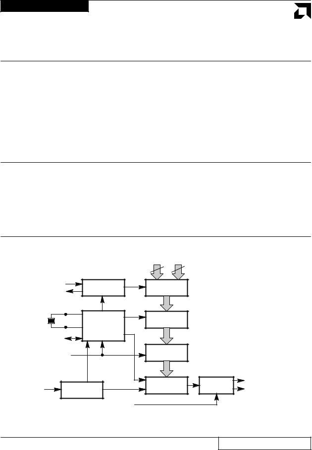
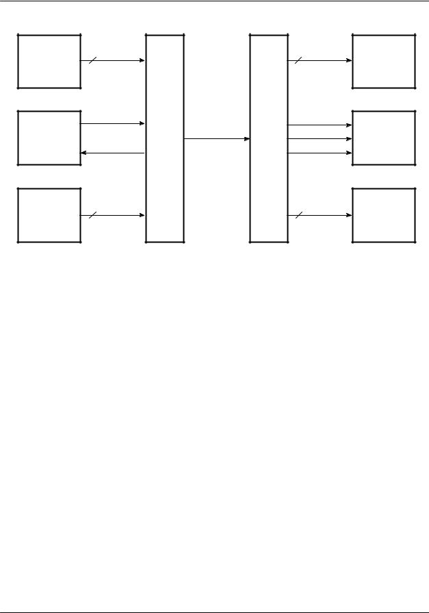
The Am7968 TAXIchip Transmitter and Am7969 TAXIchip Receiver Chipset is a general-purpose interface for very high-speed (4–17.5 Mbyte/s, 40–175 Mbaud serially) point-to-point communications over coaxial or fiber-optic media. The TAXIchip set emulates a pseudo-parallel register. They load data into one side and output it on the other, except in this case, the “other” side is separated by a long serial link.
The speed of a TAXIchip system is adjustable over a range of frequencies, with parallel bus transfer rates of 4 Mbyte/s at the low end, and up to 17.5 Mbyte/s at the high end. The flexible bus interface scheme of the TAXIchip set accepts bytes that are either 8, 9, or 10 bits wide. Byte transfers can be Data or Command signaling.
BLOCK DIAGRAM
Am7968
|
|
Data |
Command |
|
|
|
N |
M |
|
Strobe (STRB) |
Strobe & |
Input Latch |
||
Acknowledge (ACK |
Acknowledge |
|||
|
|
|||
|
X1 |
|
|
|
|
|
|
|
Oscillator |
Encoder Latch |
|
|
|
|
|
and |
|
|
|
|
|
X2 |
Clock Gen. |
|
|
|
|
Clock (CLK) |
|
|
|
|
||
Data Mode Select (DMS) |
|
Data Encoder |
|
|
||
|
|
|
|
|||
|
|
|
Shifter |
Media |
(SEROUT+) Serial Out + |
|
Test Serial In |
Serial Interface |
Interface |
(SEROUT–) Serial Out – |
|||
|
||||||
(TSERIN) |
|
|
|
|
|
|
|
|
Test/Local Select (TLS) |
|
|
07370F-1 |
|
Note: |
|
|
|
|
||
|
|
|
|
|
||
N can be 8, 9, or 10 bits; total of N + M = 12.
Publication# 07370 Rev. F Amendment /0
Issue Date: April 1994
AMD |
|
|
|
|
BLOCK DIAGRAM (continued) |
|
|
||
Am7969 |
|
|
|
|
|
|
|
(X1) |
|
|
|
|
Oscillator |
|
Serial In+ (SERIN+) |
Media |
|
and |
|
Shifter |
Clock Gen. |
|||
|
||||
Serial In– (SERIN–) |
Interface |
|
(X2) |
|
|
|
|
PLL Clock |
|
|
|
Decoder Latch |
Generator |
|
|
|
|
||
(DMS) Data Mode Select
|
Data Decoder |
Byte Sync |
(CNB) Catch Next Byte |
|
|
Logic |
(IGM) I-Got-Mine |
|
Output Latch |
|
(CLK) Clock |
|
N |
M |
(DSTRB) Data Strobe |
(VLTN) |
|
|
|
|
|
|
|
Violation |
Data Command |
(CSTRB) Command Strobe |
|
Note: |
|
|
|
N can be 8, 9, or 10 bits Total of N + M = 12 |
07370F-2 |
|
CONNECTION DIAGRAMS
Top View
Am7968
DIPs
|
|
|
|
|
|
|
ACK |
|
1 |
|
28 |
|
DI5 |
|
|
|
|
|
|
|
STRB |
|
2 |
|
27 |
|
DI4 |
SEROUT+ |
|
3 |
|
26 |
|
DI3 |
|
|
|
||||
|
|
|
|
|
||
SEROUT– |
|
4 |
|
25 |
|
DI2 |
|
|
|
||||
|
|
|
|
|
||
|
|
|
|
|
|
|
VCC2 (ECL) |
|
5 |
|
24 |
|
DI1 |
|
|
|
|
|
|
|
VCC1 (TTL) |
|
6 |
|
23 |
|
DI0 |
|
|
|
|
|
||
|
|
|
|
|
|
|
VCC3 (CML) |
|
7 |
|
22 |
|
GND1 (TTL) |
RESET |
|
|
|
|
|
|
|
8 |
|
21 |
|
GND2 (CML) |
|
DMS |
|
|
|
|
|
X1 |
|
9 |
|
20 |
|
||
TLS |
|
|
|
|
|
X2 |
|
10 |
|
19 |
|
||
|
|
|
|
|
|
|
TSERIN |
|
11 |
|
18 |
|
CLK |
|
|
|
|
|
|
|
CI0 |
|
12 |
|
17 |
|
DI6 |
CI1 |
|
|
|
|
|
DI7 |
|
13 |
|
16 |
|
||
DI9/CI2 |
|
|
|
|
|
DI8/CI3 |
|
14 |
|
15 |
|
||
|
|
|
|
|
|
07370F-3 |
|
|
|
|
|
|
Note:
Pin 1 is marked for orientation.
LCC/PLCC
|
|
|
SEROUT- |
SEROUT+ |
STRB |
ACK |
DI5 |
DI4 |
DI3 |
|
|
|
|
3 |
2 |
1 |
28 |
27 |
26 |
|
|
|
|
|
4 |
|
||||||
VCC2 (ECL) |
5 |
|
|
|
|
|
|
25 |
DI2 |
|
VCC1 (TTL) |
6 |
|
|
|
|
|
|
24 |
DI1 |
|
VCC3 (TTL) |
7 |
|
|
|
|
|
|
23 |
DI0 |
|
RESET |
8 |
|
|
|
|
|
|
22 |
GND1 (TTL) |
|
DMS |
9 |
|
|
|
|
|
|
21 |
GND2 (CML) |
|
TLS |
10 |
|
|
|
|
|
20 |
X1 |
||
TSERIN |
11 |
|
|
|
|
|
19 |
X2 |
||
|
12 |
13 |
14 |
15 |
16 |
17 |
18 |
07370F-4 |
||
|
|
|
|
|
|
|
|
|
|
|
|
|
|
CI0 |
CI1 |
DI9/CI2 |
DI8/CI3 |
DI7 |
DI6 |
CLK |
|
2 |
Am7968/Am7969 |

AMD 
CONNECTION DIAGRAMS (continued)
Top View
Am7969
DIPs |
LCC/PLCC |
|
|
|
|
|
|
|
DO3 |
|
1 |
|
28 |
|
DO4 |
DO2 |
|
|
|
|
|
DO5 |
|
2 |
|
27 |
|
||
DO1 |
|
3 |
|
26 |
|
DO6 |
|
|
|
||||
|
|
|
|
|
||
DO0 |
|
4 |
|
25 |
|
DO7 |
|
|
|
||||
|
|
|
|
|
||
|
|
|
|
|
|
|
IGM |
|
5 |
|
24 |
|
CNB |
|
|
|
|
|
|
|
RESET |
|
6 |
|
23 |
|
X2 |
|
|
|
|
|
|
|
VCC1 (TTL) |
|
7 |
|
22 |
|
X1 |
|
|
|
|
|
|
|
VCC2 (CML) |
|
8 |
|
21 |
|
GND2 (CML) |
|
|
|
|
|
||
SERIN+ |
|
|
|
|
|
GND1 (TTL) |
|
9 |
|
20 |
|
||
SERIN– |
|
|
|
|
|
CLK |
|
10 |
|
19 |
|
||
|
|
|
|
|
|
|
DMS |
|
11 |
|
18 |
|
DO8/CO3 |
DSTRB |
|
|
|
|
|
DO9/C02 |
|
12 |
|
17 |
|
||
|
|
|
|
|
|
|
CSTRB |
|
13 |
|
16 |
|
CO1 |
VLTN |
|
|
|
|
|
CO0 |
|
14 |
|
15 |
|
||
|
|
|
|
|
|
07370F-5 |
|
|
|
|
|
|
Note:
Pin 1 is marked for orientation.
|
|
|
DO0 |
DO1 |
DO2 |
DO3 |
DO4 |
DO5 |
DO6 |
|
|
|
|
3 |
2 |
1 |
28 |
27 |
26 |
|
|
|
|
|
4 |
|
||||||
IGM |
5 |
|
|
|
|
|
|
25 |
DO7 |
|
RESET |
6 |
|
|
|
|
|
|
24 |
CNB |
|
VCC1 (TTL) |
7 |
|
|
|
|
|
|
23 |
X2 |
|
VCC2 (CML) |
8 |
|
|
|
|
|
|
22 |
X1 |
|
SERIN+ |
9 |
|
|
|
|
|
|
21 |
GND2 (CML) |
|
SERIN- |
10 |
|
|
|
|
|
20 |
GND1 (TTL) |
||
DMS |
11 |
|
|
|
|
|
19 |
CLK |
||
|
12 |
13 |
14 |
15 |
16 |
17 |
18 |
|
||
|
|
|
DSTRB |
CSTRB |
VLTN |
CO0 |
CO1 |
DO9/CO2 |
DO8/CO3 |
07370F-6 |
|
|
|
|
|
|
|
|
|
|
|
LOGIC SYMBOLS
Am7968 |
Am7969 |
TLS |
DMS |
RESET |
CNB |
DMS |
RESET |
12 |
|
2 |
2 |
|
12 |
DIn/CIm |
|
SEROUT+ |
SERIN+ |
|
DOn/COm |
STRB |
|
|
|
|
VLTN |
|
|
|
|
|
|
|
|
ACK |
|
|
DSTRB |
X1 |
|
|
X1 |
|
|
|
|
|
|
|
CSTRB |
X2 |
|
|
X2 |
|
IGM |
|
|
|
|
|
|
TSERIN |
|
CLK |
|
|
CLK |
07370F-7 |
07370F-8 |
VCC = Power Supply (3) |
VCC = Power Supply (2) |
GND = Ground (2) |
GND = Ground (2) |
Am7968/Am7969 |
3 |
 AMD
AMD
ORDERING INFORMATION Standard Products
AMD standard products are available in several packages and operating ranges. The ordering number (Valid Combination) is formed by a combination of:
AM7968 |
|
D |
C |
AM7969 |
–125 |
DEVICE NUMBER/DESCRIPTION
Am7968 TAXIchip Transmitter
Am7969 TAXIchip Receiver
Valid Combinations
AM7968-125
AM7969-125
DC, JC
AM7968-175
AM7969-175
TEMPERATURE RANGE
C = Commerical (0°C to +70°C)
PACKAGE TYPE
D = 28-Pin Ceramic DIP (CD 028)
J= 28-Pin Plastic Leaded Chip Carrier (PL 028)
SPEED OPTION
-125 = Max Serial Encoded Transmission Rate is 125 MHz
-175 = Max Serial Encoded Transmission Rate is 175 MHz
Valid Combinations
Valid Combinations list configurations planned to be supported in volume for this device. Consult the local AMD sales office to confirm availability of specific valid combinations and to check on newly released combinations.
4 |
Am7968/Am7969 |

AMD 
MILITARY ORDERING INFORMATION
CPL Products
AMD products for Aerospace and Defense applications are available in several packages and operating ranges. CPL (Controlled
Products List) products are compliant with MIL-STD-883C requirements with exceptions for VCC or operating temperature. The order number (Valid Combination) is formed by a combination of:
AM7968 |
-125 |
/L |
|
C |
AM7969 |
K |
C = Controlled Product List
TEMPERATURE RANGE
K = –30 °C to 125°C
M = –55 °C to 125°C
PACKAGE TYPE
D = 28-Pin Ceramic DIP (CD 028)
L = 28-Pin Ceramic Leadless Chip
Carrier (CL 028)
SPEED OPTION
-125 = Max Serial Encoded Transmission Rate is 125 MHz
DEVICE NUMBER/DESCRIPTION
Am7968 – TAXIchip Transmitter (Local Mode only)
Am7969 – TAXIchip Receiver (Local Mode only)
Valid Combinations
Valid Combinations list configurations planned to be supported in volume for this device. Consult the local AMD sales office to confirm availability of specific valid combinations and to check on newly released combinations.
|
|
|
|
Group A Tests |
|
|
|
|
|
|
Group A tests consist of Subgroups |
||
|
|
|
|
1, 2, 3, 7, 8, 9, 10, 11. |
|
|
|
|
|
Valid Combinations |
|
||
|
|
|
|
|
|
|
Pkg |
Temps (TC) |
VCC |
CPL Part Number |
SMD Part Number |
|
APL Part Number |
|
|
|
|
|
|
|
LCC |
–30 °C to 125°C |
4.5 V to 5.5 V |
AM7968-125/LKC |
|
|
|
|
|
|
|
|
|
|
LCC |
–55 °C to 125°C |
4.75 V to 5.5 V |
|
5962-9052701M3A |
|
AM7968-125V/B3A |
|
|
|
|
|
|
|
DIP |
–30 °C to 125°C |
4.5 V to 5.5 V |
AM7968-125/DKC |
|
|
|
|
|
|
|
|
|
|
DIP |
–55 °C to 125°C |
4.75 V to 5.5 V |
|
5962-9052701MXA |
|
AM7968-125V/BXA |
|
|
|
|
|
|
|
LCC |
–30 °C to 125°C |
4.5 V to 5.5 V |
AM7969-125/LKC |
|
|
|
|
|
|
|
|
|
|
LCC |
–55 °C to 125°C |
4.75 V to 5.5 V |
|
5962-9052801M3A |
|
AM7969-125V/B3A |
|
|
|
|
|
|
|
DIP |
–30 °C to 125°C |
4.5 V to 5.5 V |
AM7969-125/DKC |
|
|
|
|
|
|
|
|
|
|
DIP |
–55 °C to 125°C |
4.75 V to 5.5 V |
|
5962-9052801MXA |
|
AM7969-125V/BXA |
|
|
|
|
|
|
|
Am7968/Am7969 |
5 |

 AMD
AMD
PIN DESCRIPTION |
Command. When it is wired to VCC, the Am7968 |
|
Am7968 TAXIchip Transmitter |
Transmitter will assume Data to be nine bits wide, with |
|
three bits of Command. If DMS is left floating (or termi- |
||
ACK |
||
nated to 1/2 VCC), the Am7968 will assume Data to be |
||
Input-Strobe Acknowledge (TTL Output) |
ten bits wide, with two bits of Command. |
|
ACK High signifies that the Am7968 is ready to accept |
GND1, GND2 |
|
new Data and Command. The timing of ACK’s response |
||
Ground Pins |
||
to STRB depends on the condition of the Input Latch (in |
||
GND1 is a TTL I/O Ground and GND2 is an internal |
||
given CLK cycle). |
||
If the Input Latch is empty, data is immediately stored |
Logic and Analog Ground. |
|
RESET |
||
and ACK closely follows STRB. If the Input Latch con- |
||
tains previously stored data when STRB is asserted, |
PLL RESET (Input) |
|
ACK is delayed until the next falling edge of CLK. Note |
This pin is normally left open, but can be momentarily |
|
that for ACK to rise STRB must maintain HIGH for both |
||
grounded to force the internal PLL to reactivate lock. |
||
of the above conditions. |
||
This allows for correction in the unlikely occurrence of |
||
|
||
CI0 – CI1 |
PLL lockup on application of power. |
|
|
Parallel Command In (TTL Inputs)
These two inputs accept parallel command information from the host system. If one or more command bits are logic “1”, the command bit pattern is latched, encoded, and transmitted in place of any pattern on the Data inputs.
RESET has an internal pull-up resistor which causes it to float high when left unconnected (50 K ohm nominal).
If this board is driven by a board Reset signal, an open drain (or open collector) style output should be used to insure the High level signal is at VCC.
CLK
Clock (TTL I/O)
CLK is an I/O pin that supplies the byte-rate clock reference to drive all internal logic. When TLS is connected to ground (Local mode), CLK is enabled as a free-running (byte-rate) clock output which runs at the Crystal Oscillator frequency; this output can be used to drive the X1 input of TAXIchip Receivers or other system logic. In Test mode CLK becomes an input. In Test Mode 1 CLK is a Byte rate input and in Test Mode 2 it is a Bit rate input.
DI0 – DI7
Parallel Data In (TTL Inputs)
These eight inputs accept parallel data from the host system, to be latched, encoded and transmitted.
DI8/CI3
Parallel Data (8) In or Command (3) In (TTL Input)
DI8/CI3 input is either Data or Command, depending upon the state of DMS.
DI9/CI2
Parallel Data (9) In or Command (2) In (TTL Input)
DI9/CI2 input is either Data or Command, depending upon the state of DMS.
DMS
Data Mode Select (Input)
Data Mode Select input determines the Data pattern width. When it is wired to GND, the Am7968 Transmitter will assume Data to be eight bits wide, with four bits of
SEROUT+, SEROUT–
Differential Serial Data Out (Differential Open Emitter ECL Outputs)
These differential ECL outputs generate data at ECL voltage levels referenced to +5.0 V. When connected to appropriated pull down resistors, they are capable of driving 50-Ω terminated lines, either directly or through isolating capacitors.
STRB
Input Strobe Signal (TTL Input)
A rising edge on the STRB input causes the Data (DI0 – DI9) or the Command (CI0 – CI3) inputs to be latched into the Am7968 Transmitter. The STRB signal is normally taken LOW after ACK has risen.
TLS
Test/Local Select (Input)
TLS input determines the mode of operation. When TLS is wired to GND, the Am7968 Transmitter assumes a Local mode connection to the media. It will output NRZI encoded data, and will enable its CLK output driver. The TLS pin should always be grounded during normal operation.
When TLS is wired to VCC (Test Mode 1),the serial data is NRZ, CLK becomes an input, and ACK timing is modified. This mode is only used for Automatic Test Equipment (ATE) testing at full speed.
When this input is left unconnected, it floats to an intermediate level which puts the Am7968 Transmitter into its Test Mode 2. In Test Mode 2, the internal clock
6 |
Am7968/Am7969 |
AMD 
X1, X2
Crystal Oscillator Inputs (Inputs)
The two crystal input pins connect to an internal parallel mode oscillator which operates at the fundamental frequency of the external crystal. The byte rate matches the crystal frequency. During normal operation, the byte rate is set by the crystal frequency.
Alternatively, X1 can be driven by an external TTL frequency source. In multiple TAXI systems this external source could be another Am7968’s CLK output.
Am7968/Am7969 |
7 |

 AMD
AMD
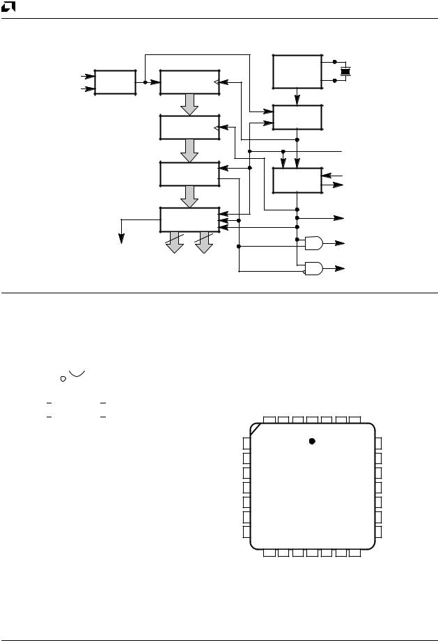
Am7969 TAXIchip Receiver
CLK
Clock (TTL Output)
This is a free-running clock output which runs at the byte rate, and is synchronous with the serial input. It falls at the time that the Decoder Latch is loaded from the Shifter, and rises at mid-byte. The CLK output of the Receiver is not suitable as a frequency source for another TAXI Transmitter or Receiver. It is intended to be used by the host system as a clock synchronous with the received data.
CNB
Catch Next Byte Input (TTL Input)
If this input is connected to the CLK output, the Receiver will be in the Local mode, and each received byte will be captured, decoded and latched to the outputs.
If the CNB input is HIGH, it allows the Am7969 Receiver to capture the first byte after a sync. The Am7969 Receiver will wait for another sync before latching the data out, and capturing another. If CNB is toggled LOW, it will react as if it had decoded a sync byte.
In Cascade mode, CNB input is typically connected to an upstream Am7969’s IGM output. The first Am7969 Receiver in line will have its CNB input connected to VCC.
For Am7969-175 applications, an inverter is required between CLK and CNB for speeds above 140 MHz. See Figure 3 and Timing Specifications T47A, T47B, T48, and T49.
CO0 – CO1
Parallel Command Out (TTL Output)
These two outputs reflect the most recent Command data received by the Am7969 Receiver.
CSTRB
Command Data Strobe (TTL Output)
The rising edge of this output signals the presence of new Command data on the CO0 – CO3 lines. Command bits are valid just before the rising edge of CSTRB.
DMS
Data Mode Select (Input)
DMS selects the Data pattern width. When it is wired to GND, the Am7969 Receiver will assume Data to be eight bits wide, with four bits of Command. When it is wired to VCC the Am7969 Receiver will assume Data to be nine bits wide, with three bits of Command. If DMS is left floating (or terminated to 1/2 VCC), the Am7969 Receiver will assume Data to be ten bits wide, with two bits of Command.
DO0 – DO7
Parallel Data Out (TTL Outputs)
These eight outputs reflect the most recent Data received by the Am7969 Receiver.
DO8/CO3
Parallel Data (8) Out or Command (3) Out (TTL Output)
DO8/CO3 output will be either a Data or Command bit, depending upon the state of DMS.
DO9/CO2
Parallel Data (9) Out or Command (2) Out (TTL Output)
DO9/CO2 output will be either a Data or Command bit, depending upon the state of DMS.
DSTRB
Output Data Strobe (TTL Output)
The rising edge of this output signals the presence of new Data on the DO0 – DO9 lines. Data is valid just before the rising edge of DSTRB.
GND1, GND2
Ground
GND1 is a TTL I/O Ground, GND2 is an internal Logic and Analog Ground.
IGM
I-Got-Mine (TTL Output)
This pin signals cascaded Am7969 Receivers that their upstream neighbor has captured its assigned data byte. IGM falls at the mid-byte when the first half of a sync byte is detected in the Shifter. It rises at mid-byte when it detects a non-sync pattern. During Local mode operation the IGM signal is undefined.
RESET
PLL RESET (Input)
This pin is normally left open, but can be momentarily grounded to force the internal PLL to reactivate lock. This allows for correction in the unlikely occurance of PLL Lockup on application of power.
RESET has an internal pull-up resistor (50 K nominal) which causes it to float high when left unconnected.
If this board is driven by a board Reset signal, an open drain (or open collector) style output should be used to insure the High level signal is at VCC.
SERIN+, SERIN–
Differential Serial Data In (ECL Inputs)
Data is shifted serially into the Shifter. The SERIN+ and SERIN– differential ECL inputs accept ECL voltage
8 |
Am7968/Am7969 |

AMD 
swings, which are referenced to +5.0 V. When SERIN– is grounded, the Am7969 is put into Test Mode; SERIN+ becomes a single-ended ECL input, the PLL clock generator is bypassed, and X1 determines the bit rate (rather than the byte rate). Both pins have internal pull down resistors which cause unterminated inputs to stay low.
VCC1, VCC2
Power Supply
VCC1 and VCC2 are +5.0 volt nominal power supply pins. VCC1 powers TTL I/O, and VCC2 powers internal Logic and Analog circuitry.
same time DOi or COi change and will be followed by either DSTRB or CSTRB. This pin goes LOW when the next valid byte is decoded.
X1, X2
Crystal Oscillator Inputs (Inputs)
These two crystal input pins connect to an internal parallel/mode oscillator which oscillates at the fundamental frequency external crystal. During normal operation, the byte rate is set by the crystal frequency. Alternatively, X1 can be driven by an external frequency source. In multiple TAXI systems, this external source could be a TAXI Transmitter’s CLK output or an external TTL frequency source.
VLTN
Violation (TTL Output)
The rising edge of this output indicates that a transmission error has been detected. It changes state at the
Am7968/Am7969 |
9 |

FUNCTIONAL DESCRIPTION |
information remains unchanged. If a Command pattern |
||
System Configuration |
is sent to the output latch or if Sync is received, CSTRB |
||
is pulsed and Data outputs remain in their previous |
|||
The TAXIchip system provides a means of connecting |
|||
state. Reception of a Sync pattern clears the Command |
|||
parallel data systems over a serial link (Figure 2). In |
outputs to all 0’s, since Sync is a legal command. |
||
LOCAL Mode (normal operation mode) each TX/RX |
Noise-induced bit errors can distort transmitted bit pat- |
||
pair is connected over a serial link which can be a Fiber |
|||
terns. The Am7969 Receiver logic detects most noise- |
|||
Optic or Copper Media (Figure 3). |
|||
induced transmission errors. Invalid bit patterns are |
|||
The Am7968 Transmitter accepts inputs from a sending |
|||
recognized and indicated by the assertion of the viola- |
|||
host system using a simple STRB/ACK handshake. |
tion (VLTN) output pin. This signal rises to a logic “1” |
||
Parallel bits are saved by the Am7968’s input latch on |
state at the same time that Data or Command outputs |
||
the rising edge of a STRB input. The input latch can be |
change and remains HIGH until a valid pattern is |
||
updated on every CLK cycle; if it still contains previously |
detected by the Data Decoder. The error detection |
||
stored data when a second STRB pulse arrives, Data is |
method used in the Receiver cannot identify bit |
||
stored in the input latch, and the second ACK response |
errors which transform one valid Command or Data pat- |
||
is delayed until the next CLK cycle. |
tern to another. Fault-sensitive systems should use ad- |
||
The inputs to an Am7968 Transmitter can be either Data |
ditional |
error checking mechanisms to guarantee |
|
message integrity. |
|||
or Command and may originate from two different parts |
|||
|
|
||
of the host system. A byte cycle may contain Data or |
Am7968 Transmitter |
||
Command, but not both. Data represents the normal |
The Transmitter accepts messages from its parallel in- |
||
data channel message traffic between host systems. |
|||
put pins (Command or Data). Once latched into an |
|||
Commands can come from a communication control |
|||
Am7968, a parallel message is encoded, serialized, and |
|||
section of the host system. Commands occur at a rela- |
|||
shifted out to the serial link. The idle time between trans- |
|||
tively infrequent rate but have priority over Data. Exam- |
|||
mitted bytes (evident by lack of STRB) is filled with |
|||
ples include communication specific commands such |
|||
Sync bytes. |
|||
as REQUEST-TO-SEND or CLEAR-TO-SEND; or |
|||
|
|
||
application specific commands such as MESSAGE- |
Am7969 Receiver |
||
ADDRESS-FOLLOWS, MESSAGE-TYPE-FOLLOWS, |
Receivers accept differential signals on the SERIN+/ |
||
INITIALIZE YOUR SYSTEM, ERROR, RETRANSMIT, |
|||
SERIN– |
input pins. This information, previously |
||
HALT, etc. |
|||
encoded by an Am7968 Transmitter, is loaded into |
|||
|
|||
The Am7968 Transmitter switches between Data and |
a decoder. |
||
Command by examining Command input patterns. All |
When serial patterns are received, they are decoded |
||
0s on Command input pins cause information on the |
|||
and routed to the appropriate outputs. If the received |
|||
Am7968’s Data input pins to be latched into the device |
|||
message is a Command, it is stored in the output latch, |
|||
on the rising edge of STRB. All other Command patterns |
|||
appears at the Command output pins, and CSTRB is |
|||
cause a Command symbol to be sent in response to an |
|||
pulsed; Data output pins continue holding the last Data |
|||
input strobe. The pattern on the Data inputs is ignored |
|||
byte and DSTRB stays inactive. If a Data message fol- |
|||
when a Command symbol is sent. In either case, if there |
|||
lows the reception of a Command, Command output |
|||
is no STRB before the next byte boundary, a Sync sym- |
|||
pins continue holding the previous Command byte and |
|||
bol will be transmitted. The sync pattern maintains link |
|||
CSTRB stays inactive. The command outputs will retain |
|||
synchronization and provides an adequate signal transi- |
|||
their states until another Command signal is received |
|||
tion density to keep the Receiver Phase-Locked-Loop |
|||
(Sync is considered to be a valid command which, when |
|||
(PLL) circuits in lock. It was chosen for its unique pattern |
|||
decoded, sets Command outputs to “0” and issues a re- |
|||
which never occurs in any Data or Command mes- |
|||
sulting CSTRB). |
|||
sages. This feature allows Sync to be used to establish |
|||
|
|
||
byte boundaries. |
Byte Width |
||
|
|||
The Sync pattern utilized by TAXIchip set keeps the |
The TAXIchip set has twelve parallel interface pins |
||
automatic gain control (AGC) fiber-optic transceiver cir- |
which are designated to carry either Command or Data |
||
cuits in their normal range because the pattern has zero |
bits. The Data Mode Select (DMS) pin on each chip can |
||
DC offset. |
be set to select one of three modes of operation: eight |
||
AMD |
Data and four Command bits, nine Data and three Com- |
||
|
|
||
The Am7969 Receiver detects the difference between
Data and Command patterns and routes each to the
mand, or ten Data and two Command. This allows the
proper Output Latch. When a new Data pattern enters
system designer to select the byte-width which best
the output latch, DSTRB is pulsed and Command
suits system needs.
10 |
Am7968/Am7969 |

|
|
AMD |
||
|
|
|
||
Am7968 Encoder/Am7969 Decoder |
pattern during each clock cycle in which no new Data or |
|||
To guarantee that the Am7969’s PLL can stay locked |
Command messages are being transmitted. |
|
|
|
|
|
|
||
onto an incoming bit stream, the data encoding scheme |
Cascade Mode (for –125 only) |
|
|
|
must provide an adequate number of transitions in each |
For very wide parallel buses, TAXI Receiver’s (commer- |
|||
data pattern. This implies a limit on the maximum time |
||||
cial temperature parts only) can be Cascaded. The |
||||
allowed between transitions. The TAXIchip set encod- |
||||
Am7969 Receivers all have their SERIN+ and SERIN– |
||||
ing scheme is based on the ANSI X3T9.5 (FDDI) com- |
||||
pins connected to the media (or an optical data link). |
||||
mittee’s 4-bit/5-bit (4B/5B) code. |
||||
IGM of each Am7969 is connected to CNB of its down- |
||||
|
||||
An ANSI X3T9.5 system used an 8-bit parallel data pat- |
stream neighbor or is left unconnected on the Receiver |
|||
tern. This pattern is divided into two 4-bit nibbles which |
farthest downstream. CNB of the first Receiver is tied |
|||
are each encoded into a 5-bit symbol. Of the thirty-two |
HIGH, making this device the only Receiver in the chain |
|||
patterns possible with these five bits, sixteen are chosen |
that can act on the first non-Sync pattern in a message |
|||
to represent the sixteen input Data patterns. Some of |
(see below). |
|
|
|
the others are used as Command symbols. Those re- |
Each TAXIchip Receiver monitors the serial link and a |
|||
maining represent invalid patterns that fail either the |
||||
special acknowledgment scheme is used to direct sym- |
||||
run-length test or DC balance tests. |
||||
bols into each of the Am7969s. When a Catch-Next- |
||||
|
||||
Transmitters in 8-bit mode use two 4B/5B encoders to |
Byte (CNB) input is HIGH, the Receiver will capture the |
|||
encode eight Data bits into a 10-bit pattern. In 9-bit |
next non-Sync symbol from the serial link. At this point, |
|||
mode, Transmitters use one 5B/6B encoder and one |
the device forces its I-Got-Mine (IGM) pin HIGH to tell |
|||
4B/5B encoder to code nine Data bits into an 11-bit pat- |
the downstream Receiver to capture the next symbol. |
|||
tern. In 10-bit mode, two 5B/6B encoders are used to |
The Receiver then waits for the Sync symbol or for its |
|||
change ten bits of Data into a 12-bit pattern (see Tables |
CNB to be set LOW before transferring the message to |
|||
1 and 2 for encoding patterns). |
its output latch. IGM is forced LOW whenever a Sync |
|||
The Am7968 Transmitter further encodes all symbols |
byte is detected or when CNB goes LOW. This IGM- |
|||
CNB exchange continues down the chain until the last |
||||
using NRZI (Non Return to Zero, Invert on Ones). NRZI |
||||
Receiver captures its respective byte. The next byte to |
||||
represents a “1” by a transition and a “0” by the lack of |
||||
appear on the serial link will be a Sync symbol which is |
||||
transition. In this system a “1” can be a HIGH-to-LOW or |
||||
detected by all of the cascaded Am7969s. On the follow- |
||||
LOW-to-HIGH transition. This combination of 4B/5B |
||||
ing Clock cycle their messages are transferred to the |
||||
and NRZI encoding ensures at least two transitions per |
||||
output latch of each device and sent to the receiving |
||||
symbol and permits a maximum of three consecutive |
||||
host. IGM pins on all Receivers are also set LOW when |
||||
non-transition bit times. The Am7969 then uses the |
||||
the first half of the Sync symbol is detected. |
|
|
||
same method to decode incoming symbols so that the |
|
|
||
|
|
|
||
whole encoding/decoding process is transparent to |
Asynchronous Operation |
|
|
|
the user. |
Inputs to the Am7968 Transmitter Input Latch can be |
|||
|
||||
Most Serially transmitted data patterns with this code |
asynchronous to its internal clock. Data STRB will latch |
|||
will have the same average amount of HIGH and LOW |
data into the Am7968 Transmitter and an internal clock |
|||
times. This near DC balance minimizes pattern-sensi- |
will transfer the data to the Encoder Latch at the first |
|||
tive decoding errors which are caused by jitter in AC- |
byte boundary. Data can be entered at any rate less |
|||
coupled systems. |
than the maximum transfer rate without regard to actual |
|||
Operational Modes |
byte boundaries. As data rates approach the TAXI |
|||
BYTE RATE, care must be taken to insure that the 2 |
||||
In normal operational mode, a single Transmitter/ |
BYTE FIFO inside TAXI Transmitter is not over filled. |
|||
STRB/ACK handshake will assure that every byte is |
||||
Receiver pair is used to transfer 8, 9, or 10 bits of parallel |
||||
transferred correctly. At higher byte rates, where delays |
||||
Data over a private serial link. (On the Am7968, the TLS |
||||
and setup/hold times make the STRB/ACK handshake |
||||
pin is tied to ground and TSERIN is left unconnected). |
||||
impractical, STRB should be synchronized with CLK. |
||||
On the Am7969, CNB must be connected to the CLK |
||||
|
|
|
||
output. The Am7969 Receiver continuously deserial- |
Synchronous Operation |
|
|
|
izes the incoming bit stream, decodes the resulting pat- |
|
|
||
The Transmitter may be strobed synchronous by tying |
||||
terns, and saves parallel data at its output latches (see |
||||
Figure 3). |
the strobe to the input clock. When doing this a provision |
|||
Local mode provides a fast and efficient parallel |
should be make to inhibit the strobe periodically to en- |
|||
sure proper byte alignment. In the absence of a strobe, |
||||
throughout because data can be transferred on every |
Syncs will be transmitted on the serial link which will al- |
|||
clock cycle. On the other hand, it is not necessary for the |
low the receiver to re-align the byte boundaries. In addi- |
|||
host to match the byte rate set by the Transmitter’s crys- |
tion it is essential that the delay between the falling edge |
|||
tal oscillator; the Am7968 automatically sends a Sync |
|
|
|
|
|
|
|
||
Am7968/Am7969 |
11 |
|||
 AMD
AMD
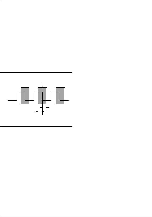
of the internal byte clock (CLK) and the rising edge of strobe does not violate tBB specification shown in the SWITCHING CHARACTERISTICS Section.
The internal byte clock controls the flow of data from the input register through the shift register. The falling edge of the internal byte clock delineates the end of one byte from the start of the next. Due to various tolerances in the PLL, the period of the internal byte clock may vary slightly. This effect may cause a shift in the location of the byte boundary with respect to the falling edge of the clock. This variation may move the byte boundary and therefore creates a window during which the part should not be strobed. This window called the t6 window, is shown in the figure below. If the part is strobed during the t6 window data will not be lost however, a sync may be added and the transmitter latency will be increased by one byte time.
Strobe Stayout Area
(t6 window)
CLK
–9/8(t1/n) + 9 ns
20 ns
07370F-9
Nominal Byte
Boundary
Sync Acquisition
In case of errors which cause Am7969 Receivers to lose byte/symbol sync, and on power-up, internal logic detects this loss-re-acquisition of sync and modifies the CLK output. CLK output is actually a buffered version of the signal which controls Data transfers inside the Am7969 Receiver on byte boundaries. Byte boundaries move when the Am7969 Receiver loses, and reacquires sync. To protect slave systems (which may use this output as a clock synchronous with the incoming
data) from having clocks which are too narrow, the output logic will stretch an output pulse when the pulse would have been less than a byte-time long. The data being processed just prior to this re-acquisition of sync will be lost. The Sync symbol, and all subsequent data will be processed correctly.
TAXI User Test Modes
TLS input can be used to force the Am7968 Transmitter into either of the two Test modes. If TLS is open or terminated to approximately VCC/2 (Test Mode 2), the internal VCO is switched out and everything is clocked directly from the CLK input. The serial output data rate will be at the CLK bit rate and not at 10X, 11X, or 12X, as is the case in normal operation. Test Mode 2 will allow testing of the logic in the Latches, Encoder, and Shifter without having to first stabilize the PLL clock multiplier. In Test Mode 1 (TLS wired to VCC), the PLL is enabled and the chip operates normally, except that the output is an NRZ stream (CLK is an input & ACK function is slightly modified). This will allow testing of all functions at full rate without needing to perform match loop tests to accommodate the data inversion characteristics of NRZI.
Differential SERIN+/SERIN– inputs can be used to force the Am7969 Receiver into its Test mode. This will allow testing of the logic in the Latches, Decoder, and Shifter without having to first stabilize the the PLL. If SERIN– is tied to ground, the internal VCO is switched out and X1 becomes the internal bit rate clock. The serial data rate will be at the CLK bit rate, not at 10X, 11X, or 12X, as is the case in normal operation. In this mode, SERIN+ becomes a single-ended serial data input with nominal 100K ECL threshold voltages (Referenced to +5 volts).
These Test Mode switches make the parts determinate, synchronous systems, instead of statistical, asynchronous ones. An automatic test system will be able to clock each part through the functional test patterns at any rate or sequence that is convenient. After the logic has been verified, the part can be put back into the normal mode, and the PLL functions verified knowing that the rest of the chip is functional.
12 |
Am7968/Am7969 |

|
|
|
AMD |
|
|
|
|||
Oscillator |
frequency (1st harmonic) and at all odd harmonics of |
|||
The Am7968 and Am7969 contain an inverting amplifier |
this frequency (even harmonic resonance is not me- |
|||
chanically possible). Unless |
otherwise constrained, |
|||
intended to form the basis of a parallel mode oscillator. |
||||
crystal oscillators operate |
at |
their fundamental |
||
The design of this oscillator considered several factors |
||||
frequencies. |
|
|
||
related to its application. |
|
|
||
|
|
|
||
The first consideration is the desired frequency accu- |
A typical crystal specification for use in this circuit is: |
|||
|
|
|
||
racy. This may be subdivided into several areas. An os- |
Fundamental Frequency 3.3 MHz–17.5 MHz ± 0.1% |
|||
cillator is considered stable if it is insensitive to |
||||
Resonance: Mode |
|
Parallel |
||
variations in temperature and supply voltage, and if it is |
|
|||
Load Capacitor (Correlation) |
|
30 pF |
||
unaffected by individual component changes and aging. |
|
|||
Operating Temperature Range |
|
0°C to 70°C |
||
The design of the TAXIchip set is such that the degree to |
|
|||
which these goals are met is determined primarily by the |
Temperature Stability |
|
±100 ppm |
|
choice of external components. Various types of crystal |
Drive Level (Correlation) |
|
2 mW |
|
are available and the manufacturers’ literature should |
Effective Series Resistance |
|
25 Ω (max) |
|
be consulted to determine the appropriate type. For |
Holder Type |
|
Low profile |
|
good temperature stability, zero temperature coefficient |
|
|||
Aging for 10 years |
|
±10 ppm |
||
capacitors should be used (Type NPO). |
|
|||
It is good practice to ground the case of the crystal to |
||||
|
||||
The mechanism by which a crystal resonates is electro- |
eliminate stray pick-up and keep all connections as |
|||
mechanical. This resonance occurs at a fundamental |
short as possible. |
|
|
|
|
|
|
|
|
RESET
Am7968 or, Am7969
Power On RESET (Optional)
X1 |
|
X2 |
||
|
|
|
|
|
|
|
|
|
|
|
|
|
|
|
|
|
|
|
|
C |
|
|
|
|
|
|
C |
|
|
|
|
|
|
||
|
|
|
|
|
|
|
|
|
|
|
|
|
|
|
|
|
|
|
|
|
|
|
|
07370F-10
C* = 220 pF for 4.0–12.5 MHz crystal, 150 pF for a 12.5–17.5 MHz Crystal.
*C determined by crystal specifications and trace capacities. Values shown are typical.
Figure 1. Connections for 4.0 MHz–17.5 MHz
Am7968/Am7969 |
13 |

 AMD
AMD
Table 1. TAXIchip Encoder Patterns
|
4B/5B Encoder Scheme |
|
|
5B/6B Encoder Scheme |
|
|||
|
|
|
|
|
|
|
|
|
|
|
4-Bit |
|
5-Bit |
|
5-Bit |
|
6-Bit |
HEX |
|
Binary |
|
Encoded |
HEX |
Binary |
|
Encoded |
Data |
|
Data |
|
Symbol |
Data |
Data* |
|
Symbol |
0 |
|
0000 |
|
11110 |
00 |
00000 |
|
110110 |
1 |
|
0001 |
|
01001 |
01 |
00001 |
|
010001 |
2 |
|
0010 |
|
10100 |
02 |
00010 |
|
100100 |
3 |
|
0011 |
|
10101 |
03 |
00011 |
|
100101 |
4 |
|
0100 |
|
01010 |
04 |
00100 |
|
010010 |
5 |
|
0101 |
|
01011 |
05 |
00101 |
|
010011 |
6 |
|
0110 |
|
01110 |
06 |
00110 |
|
010110 |
7 |
|
0111 |
|
01111 |
07 |
00111 |
|
010111 |
8 |
|
1000 |
|
10010 |
08 |
01000 |
|
100010 |
9 |
|
1001 |
|
10011 |
09 |
01001 |
|
110001 |
A |
|
1010 |
|
10110 |
0A |
01010 |
|
110111 |
B |
|
1011 |
|
10111 |
0B |
01011 |
|
100111 |
C |
|
1100 |
|
11010 |
0C |
01100 |
|
110010 |
D |
|
1101 |
|
11011 |
0D |
01101 |
|
110011 |
E |
|
1110 |
|
11100 |
0E |
01110 |
|
110100 |
F |
|
1111 |
|
11101 |
0F |
01111 |
|
110101 |
|
|
|
|
|
|
|
|
|
|
|
|
|
|
10 |
10000 |
|
111110 |
|
|
|
|
|
11 |
10001 |
|
011001 |
|
|
|
|
|
12 |
10010 |
|
101001 |
|
|
|
|
|
13 |
10011 |
|
101101 |
|
|
|
|
|
14 |
10100 |
|
011010 |
|
|
|
|
|
15 |
10101 |
|
011011 |
|
|
|
|
|
16 |
10110 |
|
011110 |
|
|
|
|
|
17 |
10111 |
|
011111 |
|
|
|
|
|
18 |
11000 |
|
101010 |
|
|
|
|
|
19 |
11001 |
|
101011 |
|
|
|
|
|
1A |
11010 |
|
101110 |
|
|
|
|
|
1B |
11011 |
|
101111 |
|
|
|
|
|
1C |
11100 |
|
111010 |
|
|
|
|
|
1D |
11101 |
|
111011 |
|
|
|
|
|
1E |
11110 |
|
111100 |
|
|
|
|
|
1F |
11111 |
|
111101 |
* Note:
HEX data is parallel input data which is represented by the 4- or 5-bit binary data listed in the column to the immediate right of HEX data. Binary bits are listed from left to right in the following order.
8-Bit Mode: D7, D6, D5, D4, (4-Bit Binary), and D3, D2, D1, D0, (4-Bit Binary)
9-Bit Mode: D8, D7, D6, D5, D4, (5-Bit Binary), and D3, D2, D1, D0, (4-Bit Binary)
10-Bit Mode: D8, D7, D6, D5, D4, (5-Bit Binary), and D9,D3, D2, D1, D0, (5-Bit Binary)
Serial bits are shifted out with the most significant bit of the most significant nibble coming out first.
14 |
Am7968/Am7969 |

|
|
|
|
|
|
|
AMD |
|
|
|
|
|
|
|
|
|
|
Table 2. TAXIchip Command Symbols |
|
|
|||
|
|
|
|
|
|
|
|
Am7968 Transmitter |
|
|
|
|
Am7969 Receiver |
||
|
|
|
|
|
|
|
|
Command Input |
|
|
|
|
Command Output |
||
|
|
|
|
|
|
|
|
|
|
|
Encoded |
|
|
|
|
HEX |
Binary |
|
Symbol |
Mnemonic |
|
HEX |
Binary |
|
|
|
|
|
|
|
|
8-Bit Mode |
|
|
|
|
|
|
|
|
|
|
|
|
|
|
|
0 |
0000 |
|
XXXXX XXXXX |
Data |
|
No Change |
No Change |
|
|
|
|
|
|
(Note 2) |
(Note 2) |
|
|
|
|
|
|
|
|
No STRB |
No STRB |
|
11000 10001 |
JK (8-bit Sync) |
|
0 |
0000 |
(Note 1) |
(Note 1) |
|
|
|
|
|
|
1 |
0001 |
|
11111 11111 |
I I |
|
1 |
0001 |
2 |
0010 |
|
01101 01101 |
TT |
|
2 |
0010 |
3 |
0011 |
|
01101 11001 |
TS |
|
3 |
0011 |
4 |
0100 |
|
11111 00100 |
I H |
|
4 |
0100 |
5 |
0101 |
|
01101 00111 |
TR |
|
5 |
0101 |
6 |
0110 |
|
11001 00111 |
SR |
|
6 |
0110 |
7 |
0111 |
|
11001 11001 |
SS |
|
7 |
0111 |
8 (Note 3) |
1000 |
|
00100 00100 |
HH |
|
8 |
1000 |
9 |
1001 |
|
00100 11111 |
HI |
|
9 |
1001 |
A (Note 3) |
1010 |
|
00100 00000 |
HQ |
|
A |
1010 |
B |
1011 |
|
00111 00111 |
RR |
|
B |
1011 |
C |
1100 |
|
00111 11001 |
RS |
|
C |
1100 |
D (Note 3) |
1101 |
|
00000 00100 |
QH |
|
D |
1101 |
E (Note 3) |
1110 |
|
00000 11111 |
Q I |
|
E |
1110 |
F (Note 3) |
1111 |
|
00000 00000 |
|
F |
1111 |
|
|
|
|
|
|
|
|
|
9-Bit Mode |
|
|
|
|
|
|
|
0 |
000 |
|
XXXXXX XXXXX |
Data |
|
No Change |
No Change |
|
|
|
|
|
|
(Note 2) |
(Note 2) |
No STRB |
No STRB |
|
011000 10001 |
LK (9-bit Sync) |
|
0 |
000 |
(Note 1) |
(Note 1) |
|
|
|
|
|
|
1 |
001 |
|
111111 11111 |
I ’ I |
|
1 |
001 |
2 |
010 |
|
011101 01101 |
T ’ T |
|
2 |
010 |
3 |
011 |
|
011101 11001 |
T’S |
|
3 |
011 |
4 |
100 |
|
111111 00100 |
I’ H |
|
4 |
100 |
|
|
|
|
|
|
|
|
5 |
101 |
|
011101 00111 |
T’R |
|
5 |
101 |
6 |
110 |
|
111001 00111 |
S’R |
|
6 |
110 |
|
|
|
|
|
|
|
|
7 |
111 |
|
111001 11001 |
S’S |
|
7 |
111 |
|
|
|
|
|
|
|
|
10-Bit Mode |
|
|
|
|
|
|
|
|
|
|
|
|
|
|
|
0 |
00 |
|
XXXXXX XXXXXX |
Data |
|
No Change |
No Change |
|
|
|
|
|
|
(Note 2) |
(Note 2) |
|
|
|
|
|
|
|
|
No STRB |
No STRB |
|
011000 100011 |
LM (10-bit Sync) |
|
0 |
00 |
(Note 1) |
(Note 1) |
|
|
|
|
|
|
1 |
01 |
|
111111 111111 |
I ’ I ’ |
|
1 |
01 |
2 |
10 |
|
011101 011101 |
T ’ T ’ |
|
2 |
10 |
3 |
11 |
|
011101 111001 |
T ’ S ’ |
|
3 |
11 |
Notes:
1.Command pattern Sync cannot be explicitly sent by Am7968 Transmitter with any combination of inputs and STRB, but is used to pad between user data.
2.A strobe with all Os on the Command input lines will cause Data to be sent. See Table 1.
3.While these Commands are legal data and will not disrupt normal operation if used occasionally, they
may cause data errors if grouped into recurrent fields. Normal PLL operation cannot be guaranteed if one or more of these commands is continuously repeated.
Am7968/Am7969 |
15 |

 AMD
AMD
Am7968 Transmitter Functional Block |
|
CLK (input is multiplied by ten (8-bit mode), eleven (9-bit |
||||
Description |
|
|
|
mode), or twelve (10-bit mode), using the internal PLL to |
||
(Refer to page 1) |
|
|
|
create the bit rate. |
|
|
|
|
|
|
|
||
Crystal Oscillator/Clock Generator |
|
The working frequency can be varied between 3.3 MHz |
||||
The serial link speed is derived from a master frequency |
and 17.5 MHz. The crystal frequency required to |
|||||
achieve the maximum 175 Mbaud on the serial link, and |
||||||
source (byte rate). This source can either be the built-in |
||||||
the resultant usable data transfer rate will be: |
||||||
Crystal Oscillator, or a clock signal applied through the |
||||||
|
|
|||||
X1 pin. This signal is buffered and sent to the CLK out- |
|
|
||||
put when Am7968 Transmitter is in Local mode. |
|
|
|
|||
|
|
|
|
|
||
|
Crystal |
|
Am7968-125 Input and Am7969-125 |
Internal |
||
Mode |
Frequency |
|
Maximum Parallel Throughput |
Divide Ratio |
||
8-Bit |
12.50 MHz |
|
80 ns/pattern (100 Mbit/sec) |
125/10 |
||
|
|
|
|
|
||
9-Bit |
11.36 MHz |
|
88 ns/pattern (102 Mbit/sec) |
125/11 |
||
|
|
|
|
|
||
10-Bit |
10.42 MHz |
|
96 ns/pattern (104 Mbit/sec) |
125/12 |
||
|
|
|
|
|
||
|
Crystal |
|
Am7968-175 Input and Am7969-175 |
Internal |
||
Mode |
Frequency |
|
Maximum Parallel Throughput |
Divide Ratio |
||
|
|
|
|
|
||
8-Bit |
17.50 MHz |
|
57.1 ns/pattern (140 Mbit/sec) |
175/10 |
||
|
|
|
|
|
||
9-Bit |
15.90 MHz |
|
62.8 ns/pattern (143 Mbit/sec) |
175/11 |
||
|
|
|
|
|
||
10-Bit |
14.58 MHz |
|
68.5 ns/pattern (145 Mbit/sec) |
175/12 |
||
Input Latch
The Am7968’s Input Latch accommodates asynchronous strobing of Data and Command by being divided into two stages.
If STRB is asserted when both stages are empty, Data or Command bits are transferred directly to the second stage of the Input Latch and ACK rises shortly after STRB. This pattern is now ready to move to the Encoder Latch at the next falling edge of CLK.
An input pattern is strobed into the first stage of the Input Latch only when the second stage is BUSY (contains previously stored data). The Transmitter will be BUSY when STRB is asserted a second time in a given CLK cycle. Contents of the first stage are not protected from subsequent STRBs within the same CLK cycle. At the falling edge of CLK, previously stored data is transferred from the second stage to the Encoder Latch and the new data is clocked into the second stage of the Input Latch. If in Local mode, ACK will rise at this time.
Encoder Latch
Input to the Encoder Latch is clocked by an internal signal which is synchronous with the shifted byte being sent on the serial link. Whenever a new input pattern is strobed into the Input Latch, the data is transferred to the Encoder Latch at the next opportunity.
Data Encoder
Encodes twelve data inputs (8, 9, 10 Data bits or 4, 3, 2 Command inputs) into 10, 11, or 12 bits. The Command data inputs control the transmitted symbol. If all Command inputs are LOW, the symbol for the Data bits will be sent. If Command inputs have any other pattern then the symbol representing that Command will be transmitted.
Shifter
The Shifter is parallel-loaded from the Encoder at the first available byte boundary, and then shifted until the next byte boundary. The Shifter is being serially loaded at all times. As data is being shifted out of the Transmitter, the shifter fills from the LSB. If parallel data is available at the end of the byte, it is parallel-loaded into the Shifter and begins shifting out during the next clock cycle. Otherwise, the serially loaded data fills the next byte. The serial data which loads into the Shifter is generated by an internal state machine which generates a repeating Sync pattern.
Media Interface
The Media Interface is differential ECL, referenced to +5 V. It is capable of driving lines terminated with 50 Ω to (VCC - 2.0) volts.
16 |
Am7968/Am7969 |
|
AMD |
||
|
|
|
|
Am7969 Receiver Functional Block |
when the first byte after a Sync symbol is transferred. |
||
Description |
Parallel outputs are made on a byte boundary, after |
||
(Refer to page 1) |
CNB falls, or when Sync is detected. |
||
Crystal Oscillator/Clock Generator |
The I-Got-Mine (IGM) signal will fall when the first half of |
||
The data recovery PLL in the Am7969 must be supplied |
|||
a Sync is detected in the Shifter or when CNB goes |
|||
with a reference frequency at the expected byte rate of |
LOW. It will remain LOW until the first half of a non-Sync |
||
the data to be recovered. The source of this frequency |
byte is detected in the Shifter, whereupon it will rise (as- |
||
can either be the built-in Crystal Oscillator, or an exter- |
suming that the CNB input is HIGH). A continuous |
||
nal clock signal applied through the X1 pin. The refer- |
stream of normal data or command bytes will cause IGM |
||
ence frequency source is then multiplied by ten (8-bit |
to go HIGH and remain HIGH. A continuous stream of |
||
mode), eleven (9-bit mode) or twelve (10-bit mode) us- |
Sync’s will cause IGM to stay LOW. IGM will go HIGH |
||
ing an internal PLL. |
during the byte before data appears at the output. This |
||
Media Interface |
feature could be used to generate an early warning of in- |
||
coming data. |
|||
|
|||
SERIN+, SERIN– inputs are to be driven by differential |
Decoder Latch |
||
ECL voltages, referenced to +5 V. Serial data at these |
|||
|
|
||
inputs will serve as the reference for PLL tracking. |
Data is loaded from the Shifter to this latch at each |
||
PLL Clock Generator |
symbol/byte boundary. It serves as the input to the |
||
Data Decoder. |
|||
|
|||
A PLL Clock recovery loop follows the incoming data |
Data Decoder |
||
and allows the encoded clock and data stream to be de- |
|||
|
|
||
coded into a separated clock and data pattern. It uses |
Decodes ten, eleven, or twelve data inputs into twelve |
||
the crystal oscillator and clock generator to predict the |
outputs. In 8-bit mode, data is decoded into either an |
||
expected frequency of data and will track jittered data |
8-bit Data pattern or a 4-bit Command pattern. In 9-bit |
||
with a characteristically small offset frequency. |
mode, data is decoded into either a 9-bit Data pattern or |
||
Shifter |
a 3-bit Command pattern. In 10-bit mode, data is de- |
||
coded into either a 10-bit Data pattern or a 2-bit Com- |
|||
|
|||
The Shifter is serially loaded from the Media Interface, |
mand pattern. |
||
using the bit clock generated by PLL. |
The decoder separates Data symbols from Command |
||
Byte Sync Logic |
|||
symbols, and causes the appropriate strobe output to |
|||
The incoming data stream is a continuous stream of |
be asserted. |
||
|
|
||
data bits, without any significant signal which denotes |
Parallel Output Latch |
||
byte boundaries. This logic will continuously monitor the |
|||
Output Latch will be clocked by the byte clock, and will |
|||
data stream, and upon discovering the reserved code |
|||
reflect the most recent data on the link. Any Data pattern |
|||
used for Am7969 Receiver Sync, will initialize a |
|||
will be latched to the Data outputs and will not affect the |
|||
synchronous counter which counts bits, and indicates |
|||
status of the Command outputs. Likewise, any Com- |
|||
byte boundaries. |
|||
mand pattern will be latched to the Command outputs |
|||
|
|||
The logic signal that times data transfers from the Shif- |
without affecting the state of the Data outputs. |
||
ter to the Decoder Latch is buffered and sent to the CLK |
Any data transfer, either Data or Command will be syn- |
||
output. CLK output from the Receiver is not suitable as a |
|||
chronous with an appropriate output strobe. However, |
|||
frequency source for another TAXI Transmitter or Re- |
|||
there will be CSTRBs when there is no active data on the |
|||
ceiver. It is intended to be used by the host system as a |
|||
link, since Sync is a valid Command code. |
|||
clock synchronous with the received data. This output is |
|||
|
|
||
synchronous with the byte boundary and is synchronous |
Any pattern which does not decode to a valid Command |
||
with the Receiver’s internal byte clock. |
|||
or Data pattern is flagged as a violation. The output of |
|||
|
|||
Byte Sync Logic is responsible for generating the inter- |
the decoder during these violations is indeterminate and |
||
will result in either a CSTRB or DSTRB output when the |
|||
nal strobe signals for Parallel Output Latches. It also |
|||
indeterminate pattern is transferred to the output latch. |
|||
generates the IGM (I-Got-Mine) signal in Test mode |
|||
|
|
||
Am7968/Am7969 |
17 |
 AMD
AMD
Command |
M |
|
M |
Command |
|
Source |
Command |
|
Command |
Destination |
|
|
Signals |
|
Signals |
|
|
Message |
STRB |
|
CSTRB |
|
|
|
|
VLTN |
Data Path |
||
Transfer |
|
|
|||
|
Am7968 |
Control |
|||
Control |
|
Am7969 |
|||
ACK |
Transmission |
DSTRB |
Logic |
||
Logic |
|||||
|
Media |
|
|
||
|
|
|
|
Data |
N |
N |
|
Data |
Source |
Data |
|
Data |
Destination |
|
|
|
||
|
Signals |
|
Signals |
|
07370F-11
Note:
N can be 8, 9, or 10 bits of parallel data; total of N + M = 12.
Figure 2. TAXIchip System Block Diagram
18 |
Am7968/Am7969 |

AMD 
Message Transfer Control Logic
|
|
|
|
|
|
|
|
|
|
|
|
|
|
|
|
|
|
|
|
|
|
|
|
|
|
|
|
|
|
|
|
|
|
|
|
Data |
|
|
|
Command |
|
|
|
|
|||||||||||||
|
|
|
|
|
|
Source |
|
|
|
|
Source |
|
|
|
|
|
||||||||||||
|
|
|
|
|
|
|
|
|
|
|
|
|
|
|
|
|
|
|
|
|
|
|
|
|
|
|
|
|
|
|
|
|
|
|
|
|
|
8 |
|
|
|
|
|
|
|
|
|
|
4 |
|
|
|
|
|
|||
|
|
|
|
|
|
|
|
|
|
|
|
|
|
|
|
|
|
|
|
|
|
|
|
|
|
|
|
|
|
|
|
|
|
DI0 |
– DI7 |
|
|
|
CI0 |
– CI3 |
STRB ACK |
||||||||||||||||
|
|
|
|
|
|
|
|
|
|
|
|
|
|
|
|
|
|
|
|
|
|
|
|
|||||
|
|
SEROUT+ |
TAXI TX #1 |
|
|
|
|
|
||||||||||||||||||||
|
|
|
|
|
|
|
||||||||||||||||||||||
|
|
SEROUT– |
|
|
|
|
|
|||||||||||||||||||||
|
|
|
|
|
|
|
||||||||||||||||||||||
|
|
|
|
|
|
|
|
(Note 1) |
|
|
|
|
|
|
|
|
|
|
|
|
|
|
||||||
|
|
|
|
|
|
|
|
(Note 1) |
|
|
|
|
|
|
X2 |
|
|
|
|
|
||||||||
|
|
TLS |
DMS |
|
X1 |
|
|
CLK |
||||||||||||||||||||
|
|
|
|
|
|
|
|
|
|
|
|
|
|
|
|
|
|
|
|
|
|
|
|
|
|
|
|
|
|
|
|
|
|
|
|
|
|
|
|
|
|
|
|
|
|
|
|
|
|
|
* |
|
|
|
|
|
|
|
|
|
|
|
|
|
|
|
|
|
|
|
|
|
|
|
|
|
|
|
|
|
|
|
|
|
||
|
|
|
|
|
|
|
|
|
|
|
|
|
|
|
|
|
|
|
|
|
|
|
|
|
|
|||
|
|
|
|
|
|
|
|
|
|
|
|
|
|
|
|
|
|
|
|
|
|
|
|
|
|
|||
|
|
|
|
|
|
|
|
|
|
|
|
|
|
|
|
3.3 MHz to |
|
|
|
|
|
|||||||
|
|
|
|
|
|
|
|
|
|
|
|
|
|
|
|
17.5 MHz |
|
|
|
|
|
|||||||
Message Transfer Control Logic
|
|
|
|
|
|
|
|
|
|
|
|
|
|
|
|
|
|
|
|
|
|
|
|
|
|
|
|
|
|
|
|
|
Data |
|
|
|
Command |
|
|
|
|
|
|
||||||||||||
|
|
|
|
Source |
|
|
|
Source |
|
|
|
|
|
|
|||||||||||||
|
|
|
|
|
|
|
|
|
|
|
|
|
|
|
|
|
|
|
|
|
|
|
|
|
|
|
|
|
|
|
|
|
|
|
|
9 |
|
|
|
|
|
|
3 |
|
|
|
|
|
|
|
|
|
|||
|
|
|
|
|
|
|
|
|
|
|
|
|
|
|
|
|
|
|
|
|
|
|
|
|
|
|
|
|
|
|
|
|
DI0 |
– DI8 |
|
|
|
CI0 |
– CI2 |
STRB |
ACK |
||||||||||||||
|
|
|
|
|
|
|
|
|
|
|
|
|
|
|
|
|
|
|
|
|
|
||||||
SEROUT+ |
TAXI TX #2 |
|
|
|
|
|
|
||||||||||||||||||||
SEROUT– |
|
|
|
|
|
|
|
|
|
|
|||||||||||||||||
TLS |
DMS |
|
|
|
X1 |
|
X2 |
|
|
|
CLK |
||||||||||||||||
|
|
|
|
|
|
|
|
|
|
|
|
|
|
|
|
|
|
|
|
|
|
|
|
|
|
|
|
|
|
|
|
|
|
|
|
|
|
|
|
|
|
|
|
|
|
|
|
|
|
|
|
|
|
|
|
|
|
|
|
|
|
|
|
|
|
|
|
|
|
|
|
|
|
|
|
|
|
|
|
|
|
|
|
(Note 2)
(Note 4)
|
3.3 MHz to |
|
|
|
|
|
17.5 MHz |
* |
|
|
|
|
|
|
|
|
|
SERIN+ SERIN– |
X1 |
X2 |
DMS |
CLOCK |
|
CNB |
TAXI RX #1 |
|
IGM |
||
|
|
|
|
|
VLTN |
DSTRB DO0– DO7 |
CO0 – CO3 |
CSTRB |
|||
|
8 |
|
4 |
|
|
Data |
|
|
Command |
||
Destination |
|
|
Destination |
||
To Other Stages
|
|
(Note 4) |
|
|
|
|
|
|
3.3 MHz to |
|
|
|
|
|
|
17.5 MHz |
|
|
|
|
|
|
|
|
* |
|
|
SERIN+ SERIN– |
X1 |
X2 |
DMS |
CLOCK |
||
CNB |
|
TAXI RX #2 |
|
|
IGM |
|
|
DO0 – DO8 |
CO0 – CO2 |
|
VLTN |
||
DSTRB |
CSTRB |
|||||
|
9 |
|
|
|
3 |
|
|
Data |
|
Command |
|
||
Destination |
|
Destination |
|
|||
|
|
Data Path Control Logic |
|
Data Path Control Logic |
|
|
|
|
|
|
|
Notes: |
|
|
07370F-12 |
||
|
|
|
|||
1. |
DMS = GND = 8 Bit Mode |
TLS = GND = Local Mode |
Pin 11 = Don’t Connect = Local Mode |
||
2. |
DMS = VCC = 9 Bit Mode |
TLS = GND = Local Mode |
Pin 11 = Don’t Connect = Local Mode |
||
3.Two 8-bit local mode systems in parallel will result in an effective data rate of 200 Mbps.
4.Use inverter for operation above 140 MHz only.
*Alternatively, the X1 inputs may be driven by external TTL frequency sources.
Figure 3. TAXIchip System in Local Mode
Am7968/Am7969 |
19 |
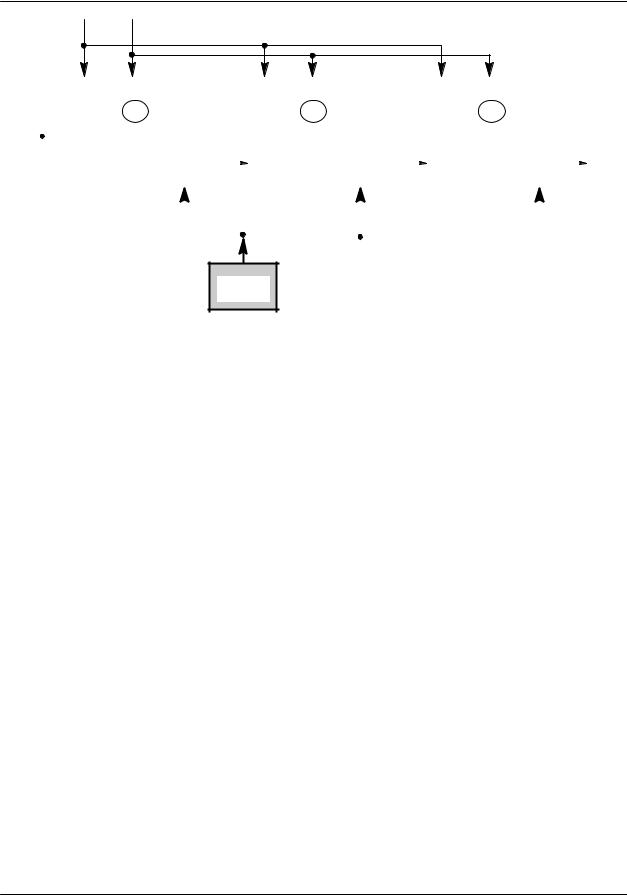
 AMD
AMD
From Serial Media
|
|
SERIN– SERIN+ |
|
|
|
|
|
|
|
|
|
|
SERIN– SERIN+ |
|
|
|
|
|
|
|
|
|
|
SERIN– SERIN+ |
|
|
|
|
|
|
|
|
|
|
||||||||||||||||||||
VCC |
|
RX1 |
|
|
|
|
|
DMS |
|
|
|
|
|
|
|
|
RX2 |
DMS |
|
|
|
|
|
|
|
|
RX3 |
DMS |
|
|
|
|
|
|
|
|
||||||||||||||||||
|
|
|
|
|
|
|
|
|
|
|
|
|
|
|
|
|
|
|
|
|
|
|
|
|
|
|
|
|
||||||||||||||||||||||||||
Am7969 |
|
|
|
|
|
|
|
|
|
|
Am7969 |
|
|
|
|
|
|
|
|
|
|
Am7969 |
|
|
|
|
|
|
|
|
|
|
||||||||||||||||||||||
|
|
|
|
|
|
|
|
|
|
|
|
|
|
|
|
|
|
|
|
|
|
|
|
|
|
|
|
|
|
|||||||||||||||||||||||||
|
|
|
|
|
|
|
|
|
|
|
|
|
|
|
|
|
|
|
|
|
|
|
|
|
|
|
|
|
|
|||||||||||||||||||||||||
|
|
|
|
|
|
|
|
|
|
|
|
|
|
|
|
|
|
|
|
|
|
|
|
|
|
|
|
|
|
|
|
|||||||||||||||||||||||
|
|
Primary RX |
|
|
|
|
|
|
|
|
|
|
|
|
|
|
|
|
|
|
|
|
|
|
|
|
|
|
|
|
|
|
|
|
|
|
|
|
|
|
|
|
|
|
|
|
||||||||
|
|
CNB |
|
|
|
|
|
IGM |
|
|
|
|
|
|
|
|
CNB |
IGM |
|
|
|
|
|
|
|
|
CNB |
IGM |
|
|
|
|
|
|
|
N/C |
||||||||||||||||||
|
|
|
|
|
|
|
|
|
|
|
|
|
|
|
|
|
|
|
|
|
|
|
|
|
|
|
|
|
|
|||||||||||||||||||||||||
|
|
CLK |
X2 |
X1 |
|
|
|
|
|
|
|
|
|
|
|
X2 |
X1 |
|
|
|
|
|
|
|
|
|
|
X2 |
X1 |
|
|
|
|
|
|
|
|
|||||||||||||||||
|
|
|
|
|
|
|
|
|
|
|
|
|
|
|
|
|
|
|
|
|
|
|
|
|
|
|
|
|
|
|
|
|
|
|
|
|
|
|
|
|
|
|
|
|
|
|
|
|
|
|
|
|
|
|
|
|
|
|
|
|
|
|
|
|
|
|
|
|
|
|
|
|
|
|
|
|
|
|
|
|
|
|
|
|
|
|
|
|
|
|
|
|
|
|
|
|
|
|
|
|
|
|
|
|
|
|
|
|
|
|
|
|
|
|
|
|
|
|
|
|
|
|
|
|
|
|
|
|
|
|
|
|
|
|
|
|
|
|
|
|
|
|
|
|
|
|
|
|
|
|
|
|
|
|
|
|
|
|
|
|
|
|
|
|
|
|
|
|
|
|
|
|
|
|
|
|
|
|
|
|
|
|
|
|
|
|
|
|
|
|
|
|
|
|
|
|
|
|
|
|
|
|
|
|
|
|
|
|
|
|
|
|
|
|
|
|
|
|
|
|
|
|
|
|
|
|
|
|
|
|
|
|
|
|
|
|
|
|
|
|
|
|
|
|
|
|
|
|
|
|
|
|
|
|
|
|
|
|
|
|
|
|
|
|
|
|
|
|
|
|
|
|
|
|
07370F-13
Crystal
OSC
Figure 4. Cascaded Receiver Clock Connections (Commercial –125 only)
20 |
Am7968/Am7969 |

AMD 
Am7968/Am7969-125 ABSOLUTE MAXIMUM RATINGS
StorageTemperature . . . . . . . . . . . . –65 °C to +150°C
Ambient Temperature
Under Bias . . . . . . . . . . . . . . . . . . . –55 °C to +125°C
Supply Voltage to Ground
Potential Continuous . . . . . . . . . . . . –0.5 V to +7.0 V
DC Voltage Applied to
Outputs . . . . . . . . . . . . . . . . . . . . . –0.5 V to V CC Max DC Input Voltage . . . . . . . . . . . . . . . –0.5 V to +5.5 V DC Output Current . . . . . . . . . . . . . . . . . . . ±100 mA DC Input Current . . . . . . . . . . . . . –30 mA to +5.0 mA
Stresses above those listed under Absolute Maximum Ratings may cause permanent device failure. Functionality at or above these limits is not implied. Exposure to absolute maximum ratings for extended periods may affect device reliability.
OPERATING RANGES
Commercial (C) Devices
Temperature (TA) . . . . . . . . . . . . . . . . . 0°C to +70°C Supply Voltage (VCC) . . . . . . . . . . . . +4.5 V to +5.5 V
Operating ranges define those limits between which the functionality of the device is guaranteed.
Am7968/Am7969-125 |
21 |

 AMD
AMD
DC CHARACTERISTICS over operating range unless otherwise specified Am7968-125 TAXIchip Transmitter
Parameter |
|
|
|
|
|
|
|
Symbol |
Parameter Description |
Test Conditions (Note 1) |
Min |
Max |
Unit |
||
|
|
|
|
|
|
|
|
Bus Interface Signals: DI0–DI7, DI8/CI3, DI9/CI2, CI0–CI1, STRB, ACK, CLK |
|
|
|
||||
VOH1 |
Output HIGH Voltage |
VCC = Min, IOH = –1 mA |
2.4 |
|
V |
||
|
ACK |
VIN = 0 or 3 V |
|
|
|
|
|
|
|
|
|
|
|
|
|
VOH2 |
Output HIGH Voltage |
VCC = Min, IOH = –3 mA |
2.4 |
|
V |
||
|
CLK |
VIN = 0 or 3 V |
|
|
|
|
|
|
|
|
|
|
|
|
|
VOL |
Output LOW Voltage |
VCC = Min, IOL = 8 mA |
|
0.45 |
V |
||
|
ACK, CLK |
VIN = 0 or 3 V |
|
|
|
|
|
|
|
|
|
|
|
|
|
VIH |
Input HIGH Voltage |
VCC = Max (Note 9) |
2.0 |
|
V |
||
|
|
|
|
|
|
|
|
VIL |
Input LOW Voltage |
VCC = Max (Note 9) |
|
0.8 |
V |
||
|
|
|
|
|
|
|
|
VI |
Input Clamp Voltage |
VCC = Min IIN = –18 mA |
|
–1.5 |
V |
||
|
|
|
|
|
|
|
|
IIL |
Input LOW Current |
VCC = Max, VIN |
= 0.4 V |
|
–400 |
A |
|
|
|
|
|
|
|
|
|
IIH |
Input HIGH Current |
VCC = Max, VIN |
= 2.7 V |
|
50 |
A |
|
|
|
|
|
|
|
|
|
II |
Input Leakage Current |
VCC = Max, |
|
All Inputs |
|
50 |
A |
|
|
VIN = 5.5 V |
|
Except CLK |
|
|
|
|
|
|
|
|
|
|
|
|
|
|
|
CLK Input |
|
150 |
A |
|
|
|
|
|
|
|
|
ISC |
Output Short Circuit |
(Note 4) |
|
|
–15 |
–85 |
mA |
|
Current ACK, CLK |
|
|
|
|
|
|
|
|
|
|
|
|
|
|
Serial Interface Signals: SEROUT+, SEROUT– |
|
|
|
|
|
||
|
|
|
|
|
|
|
|
VOH |
Output HIGH Voltage |
VCC = Min ECL Load |
VCC |
VCC |
V |
||
|
|
|
|
|
–1.025 |
–0.88 |
|
|
|
|
|
|
|
|
|
VOL |
Output LOW Voltage |
VCC = Min ECL Load |
VCC |
VCC |
V |
||
|
|
|
|
|
–1.81 |
–1.62 |
|
|
|
|
|
|
|
|
|
Miscellaneous Signals: X1, VCC1, VCC2, VCC3 |
|
|
|
|
|
||
|
|
|
|
|
|
|
|
VIHX |
Input HIGH Voltage X1 |
|
|
|
2.0 |
|
V |
|
|
|
|
|
|
|
|
VILX |
Input LOW Voltage X1 |
|
|
|
|
0.8 |
V |
|
|
|
|
|
|
|
|
IILX |
Input LOW Current X1 |
VIN = 0.45 V |
|
|
|
–900 |
A |
|
|
|
|
|
|
|
|
IIHX |
Input HIGH Current X1 |
VIN = 2.4 V |
|
|
|
+600 |
A |
|
|
|
|
|
|
|
|
ICC |
Supply Current |
SEROUT = ECL |
|
Pin VCC1 (TTL) |
|
20 |
mA |
|
|
Load, DMS = 0 |
|
|
|
|
|
|
|
|
Pin VCC2 (ECL) |
|
45 |
mA |
|
|
|
VCC1 = VCC2 = |
|
|
|||
|
|
|
|
|
|
|
|
|
|
VCC3 = Max |
|
Pin VCC3 (CML) |
|
200 |
mA |
|
|
|
|
|
|
|
|
*See notes following end of Switching Characteristics tables.
22 |
Am7968/Am7969-125 |

|
|
|
|
|
|
AMD |
|
Am7969-125 TAXIchip Receiver |
|
|
|
|
|
|
|
Parameter |
|
|
|
|
|
|
|
Symbol |
Parameter Description |
Test Conditions (Note 1) |
Min |
Max |
|
Unit |
|
|
|
|
|
|
|
|
|
Bus Interface Signals: DO0–DO7, DO8/CO3, DO9/CO2, CO0–CO1, DSTRB, CSTRB, IGM, CLK, CNB, VLTN |
|
|
|||||
|
|
|
|
|
|
|
|
VOH |
Output HIGH Voltage |
VCC = Min, IOH = –1 mA |
2.4 |
|
|
V |
|
|
|
VIN = 0 or 3 V |
|
|
|
|
|
|
|
|
|
|
|
|
|
VOL |
Output LOW Voltage |
VCC = Min, IOL = 8 mA |
|
0.45 |
|
V |
|
|
|
VIN = 0 or 3 V |
|
|
|
|
|
|
|
|
|
|
|
|
|
VIH |
Input HIGH Voltage |
VCC = Max (Note 9) |
|
2.0 |
|
|
V |
|
|
|
|
|
|
|
|
VIL |
Input LOW Voltage |
VCC = Max (Note 9) |
|
|
0.8 |
|
V |
|
|
|
|
|
|
|
|
VI |
Input Clamp Voltage |
VCC = Min, IIN = –18 mA |
|
–1.5 |
|
V |
|
|
|
|
|
|
|
|
|
IIL |
Input LOW Current |
VCC = Max, VIN = 0.4 V |
|
–400 |
|
A |
|
|
|
|
|
|
|
|
|
IIH |
Input HIGH Current |
VCC = Max, VIN = 2.7 V |
|
50 |
|
A |
|
|
|
|
|
|
|
|
|
II |
Input Leakage Current |
VCC = Max, VIN = 5.5 V |
|
50 |
|
A |
|
|
|
|
|
|
|
|
|
ISC |
Output Short Circuit |
|
|
–15 |
–85 |
|
mA |
|
Current (Note 4) |
|
|
|
|
|
|
|
|
|
|
|
|
|
|
Serial Interface Signals: SERIN+, SERIN– |
|
|
|
|
|
|
|
|
|
|
|
|
|
|
|
VIHS |
Input HIGH Voltage |
(Notes 9, 21) |
|
VCC |
VCC |
|
V |
|
SERIN+ |
|
|
–1.165 |
–0.88 |
|
|
|
|
|
|
|
|
|
|
VILS |
Input LOW Voltage |
(Notes 9, 21) |
|
VCC |
VCC |
|
V |
|
SERIN+ |
|
|
–1.81 |
–1.475 |
|
|
|
|
|
|
|
|
|
|
VTHT |
Test Mode Threshold |
VCC = Max |
|
|
0.25 |
|
V |
|
SERIN– |
|
|
|
|
|
|
|
|
|
|
|
|
|
|
VDIF |
Differential Input Voltage |
|
|
0.3 |
1.1 |
|
V |
|
|
|
|
|
|
|
|
VICM |
Input Common Mode |
(Note 6) |
|
3.05 |
VCC |
|
V |
|
Voltage |
|
|
|
–0.55 |
|
|
|
|
|
|
|
|
|
|
IIL |
Input LOW Current |
VCC = Max, VIN = VCC –1.81 V |
0.5 |
|
|
A |
|
|
|
|
|
|
|
|
|
IIH |
Input HIGH Current |
VCC = Max, |
|
|
220 |
|
A |
|
|
VIN = VCC –0.88 V |
|
|
|
|
|
|
|
|
|
|
|
|
|
Miscellaneous Signals: X1, VCC1, VCC2 |
|
|
|
|
|
|
|
|
|
|
|
|
|
|
|
VIHX |
Input HIGH Threshold X1 |
|
|
2.0 |
|
|
V |
|
|
|
|
|
|
|
|
VILX |
Input LOW Threshold X1 |
|
|
|
0.8 |
|
V |
|
|
|
|
|
|
|
|
IILX |
Input LOW Current X1 |
VIN = 0.45 V |
|
|
–900 |
|
A |
|
|
|
|
|
|
|
|
IIHX |
Input HIGH Current X1 |
VIN = 2.4 V |
|
|
+600 |
|
A |
|
|
|
|
|
|
|
|
ICC |
Supply Current |
VCC1 = VCC2 = Max |
Pin VCC1 (TTL) |
|
50 |
|
mA |
|
|
|
|
|
|
|
|
|
|
DMS = 0 V |
Pin VCC2 (CML) |
|
300 |
|
mA |
|
|
|
|
|
|
|
|
Am7968/Am7969-125 |
23 |

 AMD
AMD
SWITCHING CHARACTERISTICS (Note 20)
Am7968-125 TAXIchip Transmitter (Notes 10, 13, 22)
|
Parameter |
|
|
|
|
|
|
|
|
|
|
|
No. |
Symbol |
Parameter Description |
Test Conditions |
|
|
Min |
|
|
Max |
Units |
||
Bus Interface Signals: DI0–DI7, DI8/CI3, DI9/CI2, CI0–CI1, STRB, ACK, CLK |
|
|
|
|
|
|
|
|
|
|||
|
|
|
|
|
|
|
|
|
|
|
|
|
1 |
tP |
CLK Period |
|
|
|
8n |
|
|
25n |
ns |
||
2 |
tPW |
CLK Pulse Width HIGH |
|
|
|
30 |
|
|
|
|
|
ns |
3 |
tPW |
CLK Pulse Width LOW |
|
|
|
30 |
|
|
|
|
|
ns |
|
|
|
|
|
|
|
|
|
|
|
|
|
4 |
tPW |
STRB Pulse Width HIGH (Note 7) |
|
|
|
15 |
|
|
|
|
|
ns |
5 |
tPW |
STRB Pulse Width LOW |
|
|
|
15 |
|
|
|
|
|
ns |
|
|
|
|
|
|
|
|
|
|
|
|
|
6 |
tBB |
Internal Byte Boundary to CLK↓ |
|
|
–9t 1 |
|
|
|
20 |
ns |
||
|
|
(Note 11) |
|
|
8n +9 |
|
|
|
|
|
|
|
9 |
tS |
Data–STRB Setup Time |
|
|
|
5 |
|
|
|
|
|
ns |
10 |
tH |
Data–STRB Hold Time |
|
|
|
15 |
|
|
|
|
|
ns |
11 |
tH |
ACK↑ to STRB↓ Hold (Note 8) |
TTL Output Load |
|
|
0 |
|
|
|
|
|
ns |
|
|
|
|
|
|
|
|
|
|
|
|
|
12 |
tH |
ACK↓ to STRB↑ Hold |
TTL Output Load |
|
|
0 |
|
|
|
|
|
ns |
13 |
tPD |
STRB↑ to ACK↑ (Note 18) |
TTL Output Load |
|
|
|
|
|
|
40 |
ns |
|
14 |
tPD |
STRB↓ to ACK↓ |
TTL Output Load |
|
|
|
|
|
|
23 |
ns |
|
|
|
|
|
|
|
|
|
|
|
|
|
|
15 |
tPD |
CLK↓ to ACK↑ (Note 18) |
TTL Output Load |
|
|
|
|
|
3t1 |
+ 33 |
ns |
|
|
|
|
|
|
|
|
|
|
n |
|
|
|
Serial Interface Signals: SEROUT+, SEROUT– (Note 2) |
|
|
|
|
|
|
|
|
|
|
||
|
|
|
|
|
|
|
|
|
|
|
|
|
22 |
tSK |
SEROUT± Skew |
ECL Output Load |
|
–200 |
+200 |
ps |
|||||
23 |
tR |
SEROUT± Output Rise Time |
ECL Output Load |
|
|
.45 |
|
|
|
|
2 |
ns |
24 |
tF |
SEROUT± Output Fall Time |
ECL Output Load |
|
|
.45 |
|
|
|
|
2 |
ns |
26 |
tPW |
SEROUT ± Pulse Width LOW |
ECL Output Load |
|
t1 |
– 5% |
|
|
t1 |
|
+ 5% |
ns |
|
|
|
|
|
n |
|
|
n |
|
|
||
27 |
tPW |
SEROUT ± Pulse Width HIGH |
ECL Output Load |
|
t1 |
– 5% |
|
|
t1 |
|
+ 5% |
ns |
|
|
|
|
|
n |
|
|
n |
|
|
||
Miscellaneous Signals: X1 (Note 15) |
|
|
|
|
|
|
|
|
|
|
||
|
|
|
|
|
|
|
|
|
|
|
|
|
29 |
tPW |
X1 Pulse Width HIGH (Note 12) |
TTL Output Load on CLK |
|
|
35 |
|
|
|
|
|
ns |
|
|
|
|
|
|
|
|
|
|
|
|
|
30 |
tPW |
X1 Pulse Width LOW (Note 12) |
TTL Output Load on CLK |
|
|
35 |
|
|
|
|
|
ns |
|
|
|
|
|
|
|
|
|
|
|
|
|
32 |
tPD |
X1 ↑ to CLK↑ |
TTL Load |
|
|
|
|
|
|
32 |
ns |
|
|
|
|
|
|
|
|
|
|
|
|
|
|
33 |
tPD |
X1 ↓ to CLK↓ |
TTL Load |
|
|
|
|
|
|
32 |
ns |
|
|
|
|
|
|
|
|
|
|
|
|
|
|
24 |
Am7968/Am7969-125 |
|
|
|
|
|
|
|
|
|
|
|
|
|
|
|
|
|
|
|
|
|
AMD |
|
Am7969-125 TAXIchip Receiver (Notes 13, 14, 22) |
|
|
|
|
|
|
|
|
|
|
|
|
|
|
|
|
|
|
|
|
||
|
|
|
|
|
|
|
|
|
|
|
|
|
|
|
|
|
|
|
|
|
|
|
|
Parameter |
|
|
|
|
|
|
|
|
|
|
|
|
|
|
|
|
|
|
|
|
|
No. |
Symbol |
Parameter Description |
Test Conditions |
|
|
|
|
Min |
|
|
|
Max |
Unit |
|||||||||
Bus Interface Signals: |
DO0–DO7,DO8/CO3,DO9/CO2,CO0–CO1,DSTRB,CSTRB, IGM,CLK,CNB,VLTN |
|
||||||||||||||||||||
|
|
|
|
|
|
|
|
|
|
|
|
|
|
|
|
|
|
|
|
|
||
35 |
tP |
CLK Period (Note 24) |
|
|
|
|
|
|
8n |
|
|
25n |
ns |
|||||||||
|
|
|
|
|
|
|
|
|
|
|
|
|
|
|
|
|
|
|
|
|
|
|
36 |
tPD |
Data Valid to STRB↑ Delay |
TTL Output Load |
|
|
|
|
2t35 |
|
|
|
|
|
|
|
ns |
||||||
|
|
|
|
|
|
|
|
|
n |
|
|
|
|
|
|
|
|
|
|
|
||
37 |
tPD |
CLK↓ to STRB↑ |
TTL Output Load |
|
|
|
|
|
|
|
|
|
|
|
|
2t35 |
+15 |
ns |
||||
|
|
|
|
|
|
|
|
|
|
|
|
|
|
|
|
|
n |
|
|
|||
38 |
tPD |
CLK↑ to STRB↓ |
TTL Output Load |
|
|
|
t35 |
–7 |
|
|
|
|
|
|
|
ns |
||||||
|
|
|
|
|
|
|
n |
|
|
|
|
|
|
|
|
|
|
|
|
|
||
38a |
tPD |
STRB↑ to CLK↑ (Note 23) |
TTL Output Load |
|
3t35 |
–14 |
|
|
|
|
|
|
|
ns |
||||||||
|
|
|
|
|
|
|
|
|
|
|
||||||||||||
|
|
n |
|
|
|
|
|
|
|
|||||||||||||
39 |
tPD |
CLK↓ to Data Valid Delay |
TTL Output Load |
|
|
|
|
|
|
|
|
|
|
|
- |
|
t35 |
+23 |
ns |
|||
|
|
|
|
|
|
|
|
|
|
|
|
|
|
|||||||||
|
|
|
|
|
|
|
|
|
|
|
|
|
n |
|||||||||
|
|
|
|
|
|
|
|
|
|
|
|
|
|
|
|
|
|
|
|
|
||
40 |
tPW |
STRB Pulse Width HIGH |
TTL Output Load |
|
|
|
|
5t35 |
|
|
|
5t35 |
ns |
|||||||||
|
|
|
|
|
|
|
|
2n |
|
|
|
|
n |
|
|
|
||||||
|
|
|
|
|
|
|
|
|
|
|
|
|
|
|
|
|
|
|
|
|
|
|
41 |
tPW |
CLK Pulse Width HIGH |
TTL Output Load |
|
5t35 |
–15 |
|
|
|
|
|
|
|
ns |
||||||||
|
|
|
|
|
|
n |
|
|
|
|
|
|
|
|
|
|||||||
|
|
|
|
|
|
|
|
|
|
|
|
|
|
|
|
|
||||||
42 |
tPW |
CLK Pulse Width LOW |
TTL Output Load |
|
5t35 |
–15 |
|
|
|
|
|
|
|
ns |
||||||||
|
|
|
|
|
|
n |
|
|
|
|
|
|
|
|
|
|||||||
|
|
|
|
|
|
|
|
|
|
|
|
|
|
|
|
|
||||||
43 |
tPD |
SERIN to CLK↓ Delay |
TTL Output Load |
|
t35 |
+17 |
|
2t35 |
+26 |
ns |
||||||||||||
|
|
|
|
|
2n |
|
|
|
n |
|
|
|||||||||||
44 |
tPD |
CLK↑ to IGM↓ |
TTL Output Load |
|
|
|
|
|
|
|
|
|
|
|
|
2t35 |
|
+7 |
ns |
|||
|
|
|
|
|
|
|
|
|
|
|
|
n |
||||||||||
|
|
|
|
|
|
|
|
|
|
|
|
|
|
|
|
|
|
|
||||
|
|
|
|
|
|
|
|
|
|
|
|
|
|
|
|
|
|
|
|
|
|
|
45 |
tPD |
CLK↑ to IGM↑ |
TTL Output Load |
|
|
|
|
|
|
|
|
|
|
|
|
2t35 |
|
+10 |
ns |
|||
|
|
|
|
|
|
|
|
|
|
|
|
n |
||||||||||
|
|
|
|
|
|
|
|
|
|
|
|
|
|
|
|
|
|
|
||||
|
|
|
|
|
|
|
|
|
|
|
|
|
|
|
|
|
|
|
|
|
|
|
46 |
tPD |
CNB↓ to IGM↓ |
TTL Output Load |
|
|
|
|
|
|
|
|
|
|
|
|
20 |
|
ns |
||||
47 |
tS |
CNB↑ to CLK↑ Setup Time |
|
- |
|
|
2t35 |
–32 |
|
|
|
|
|
|
|
ns |
||||||
|
|
(Note 5) |
|
|
|
|
n |
|
|
|
|
|
|
|
|
|
||||||
|
|
|
|
|
|
|
|
|
|
|
|
|
|
|
||||||||
47A |
tS |
CNB↓ to CLK↑ Setup Time |
|
- |
|
|
t35 |
–31 |
|
|
|
|
|
|
|
ns |
||||||
|
|
(Note 19) |
|
|
|
|
n |
|
|
|
|
|
|
|
|
|
||||||
|
|
|
|
|
|
|
|
|
|
|
|
|
|
|
|
|
|
|||||
48 |
tH |
CNB↓ to CLK↑ Hold |
|
|
|
2t35 |
+5 |
|
|
|
|
|
|
|
ns |
|||||||
|
|
|
|
|
|
|
|
|
|
|
|
|
|
|
|
|||||||
|
|
|
|
n |
|
|
|
|
|
|
|
|||||||||||
|
|
|
|
|
|
|
|
|
|
|
|
|
|
|||||||||
|
|
|
|
|
|
|
|
|
|
|
|
|
|
|
|
|
||||||
49 |
tPW |
CNB Pulse Width LOW |
|
|
|
|
|
2t35 |
|
|
|
|
|
|
|
ns |
||||||
|
|
|
|
|
|
|
|
|
|
|
|
|
|
|
|
|
||||||
|
|
|
|
|
|
n |
|
|
|
|
|
|
|
|
|
|
||||||
|
|
|
|
|
|
|
|
|
|
|
|
|
|
|
|
|
|
|
|
|
|
|
Serial Interface Signals: SERIN+, SERIN– |
|
|
|
|
|
|
|
|
|
|
|
|
|
|
|
|
|
|
|
|
||
|
|
|
|
|
|
|
|
|
|
|
|
|
|
|
|
|
|
|
|
|||
57 |
tJ |
SERIN± Peak to Peak Input Jitter |
|
|
|
|
|
|
|
|
|
|
|
|
|
5 |
|
|
ns |
|||
|
|
Tolerance (Note 16) |
|
|
|
|
|
|
|
|
|
|
|
|
|
|
|
|
|
|
|
|
|
|
|
|
|
|
|
|
|
|
|
|
|
|
|
|
|
|
|
|
|
|
|
Miscellaneous Signals: X1 (Note 15) |
|
|
|
|
|
|
|
|
|
|
|
|
|
|
|
|
|
|
|
|
||
|
|
|
|
|
|
|
|
|
|
|
|
|
|
|
|
|||||||
60 |
tPW |
X1 Pulse Width HIGH |
|
|
35 |
|
|
|
|
|
|
|
|
|
ns |
|||||||
|
|
|
|
|
|
|
|
|
|
|
|
|
|
|
|
|||||||
61 |
tPW |
X1 Pulse Width LOW |
|
|
35 |
|
|
|
|
|
|
|
|
|
ns |
|||||||
|
|
|
|
|
|
|
|
|
|
|
|
|
|
|
|
|
|
|
|
|
|
|
Am7968/Am7969-125 |
25 |

 AMD
AMD
(Page intentionally left blank)
26 |
Am7968/Am7969-175 |
 Loading...