

Page 1

AMD 780E
Databook
Technical Reference Manual
Rev. 3.10
P/N: 45732_rs780e_ds_pub
© 2009 Advanced Micro Devices, Inc.
Page 2

Please note that in this databook, references to "DVI" and "HDMI" refer to the capa bility of the TMDS interface, multiplexed on the PCI-E external graphics interface, to enable
DVI or HDMI through passive enabling circuitries. Any statement in this databook on any DVI or HDMI-related functionality must be understood in that context.
Advanced Micro Devices, Inc., will not provide any indemnity, pay any royalty, nor provide any license/sublicense to any:
(a) Intellectual property rights relating to any of the following: (i) Macrovision for its Analog Protection System ("APS") technologies; (ii) Advanced Television Systems
Committee (ATSC) standard and related technologies; or (iii) the High Definition Multimedia Interface (HDMI) standard and related technologies; or
(b) Audio and/or video codecs or any industry standard technology (e.g., technology or specifications promulgated by any standards development organization, consortium,
trade association, special interest group or like entity).
This device is protected by U.S. patent numbers 5,583,936; 6,516,132; 6,836,5 49; and 7,050,698 and other intellectual property rights. The use of Macrovision's copy protection
technology in the device must be authorized by Macrovision and is intended for home and other limited pay-per-view uses only, unless otherwise authorized in writing by
Macrovision. Reverse engineering or disassembly is prohibited.
This device may only be sold or distributed to: (i) a Macrovision Authorized Buyer, (ii) a customer (PMA Customer) who has executed a Proprietary Materials Agreement
(PMA) with Macrovision that is still in effect, (iii) a contract manufacturer approved by Macrovision to purchase this device on behalf of a Macrovision Authorized Buyer or
a PMA Customer, or (iv) a distributor who has executed a Macrovision-specified distribution agreement with ATI.
Trademarks
AMD, the AMD Arrow logo, AMD Athlon, and combinations thereof, ATI, ATI logo, ATI Radeon, ATI Avivo, PowerPlay, PowerShift, PowerXpress, ATI HyperMemory,
3Dc, Cool'n'Quiet, AMD OverDrive, and AMD PowerNow! are trademarks of Advanced Micro Devices, Inc.
DisplayPort is a trademark of VESA.
HDMI, the HDMI Logo and High-Definition Multimedia Interface are trademarks or registered trademarks of HDMI Licensing LLC.
HyperTransport is a licensed trademark of the HyperTransport Technology Consortium.
2
C is a trademark of Philips.
I
Linux is a registered trademark of Linus Torvalds.
Macrovision is a registered trademark of Macrovision Corporation in the United States and/or other countries.
Microsoft, Windows, Windows Vista, DirectDraw, and DirectX are registered trademarks of Microsoft Corporation.
OpenGL is a registered trademark of SGI.
PCI Express is a registered trademark of PCI-SIG.
WinBench is a registered trademark of Ziff Davis, Inc.
Other product names used in this publication are for identification purposes only and may be trademarks of their respective companies.
Disclaimer
The contents of this document are provided in connection with Advanced Micro Devices, Inc. ("AMD") products. AMD makes no representations or warranties with respect
to the accuracy or completeness of the contents of this publication and reserves the right to make changes to specifications and product descriptions at any time without notice.
No license, whether express, implied, arising by estoppel, or otherwise, to any intellectual property rights are granted by this publication. Except as set forth in AMD's Standard
Terms and Conditions of Sale, AMD assumes no liability whatsoever, and disclaims any express or implied warranty, relating to its products including, but not limited to, the
implied warranty of merchantability, fitness for a particular purpose, or infringement of any intellectual property right.
AMD's products are not designed, intended, authorized or warranted for use as components in systems intended for surgical implant into the body, or in other applications
intended to support or sustain life, or in any other application in which the failure of AMD's product could create a situation where personal injury, death, or severe property or
environmental damage may occur. AMD reserves the right to discontinue or make changes to its products at any time without notice.
© 2009 Advanced Micro Devices, Inc. All rights reserved.
Page 3

Table of Contents
Chapter 1: Overview
1.1 Introducing the AMD 780E ................................................................................................................................................1-1
1.2 RS780E Features.................................................................................................................................................................1-2
1.2.1 CPU HyperTransport™ Interface.........................................................................................................................1-2
1.2.2 Memory Interface .................................................................................................................................................1-2
1.2.3 ATI HyperMemory™...........................................................................................................................................1-2
1.2.4 PCI Express® Interface ........................................................................................................................................1-3
1.2.5 A-Link Express II Interface..................................................................................................................................1-4
1.2.6 2D Acceleration Features .....................................................................................................................................1-4
1.2.7 3D Acceleration Features .....................................................................................................................................1-4
1.2.8 Motion Video Acceleration Features....................................................................................................................1-5
1.2.9 Multiple Display Features ....................................................................................................................................1-5
1.2.10 Integrated LVDS/TMDS (LVTM) Interface ........................................................................................................1-7
1.2.11 DVI/HDMI™ .......................................................................................................................................................1-7
1.2.12 DisplayPort™ Interface........................................................................................................................................1-7
1.2.13 Integrated HD Audio Controller and Codec.........................................................................................................1-8
1.2.14 Clock Generation..................................................................................................................................................1-8
1.2.15 Power Management Features ...............................................................................................................................1-8
1.2.16 PC Design Guide Compliance..............................................................................................................................1-8
1.2.17 Test Capability Features .......................................................................................................................................1-9
1.2.18 Additional Features ..............................................................................................................................................1-9
1.2.19 Packaging .............................................................................................................................................................1-9
1.3 Software Features................................................................................................................................................................1-9
1.4 Branding Diagram.............................................................................................................................................................1-10
1.5 Graphics Device ID and Graphics Engine Clock Speed...................................................................................................1-10
1.6 Conventions and Notations ...............................................................................................................................................1-10
1.6.1 Pin Names...........................................................................................................................................................1-10
1.6.2 Pin Types ............................................................................................................................................................1-10
1.6.3 Numeric Representation .....................................................................................................................................1-11
1.6.4 Register Field......................................................................................................................................................1-11
1.6.5 Hyperlinks ..........................................................................................................................................................1-11
1.6.6 Acronyms and Abbreviations .............................................................................................................................1-11
Chapter 2: Functional Descriptions
2.1 Host Interface......................................................................................................................................................................2-1
2.2 Side-Port Memory Interface................................................................................................................................................2-3
2.2.1 DDR2 Memory Interface......................................................................................................................................2-3
2.2.1.1 Supported DDR2 Components 4
2.2.1.2 Row and Column Addressing 4
2.2.2 DDR3 Memory Interface......................................................................................................................................2-5
2.2.2.1 Supported DDR3 Components 5
2.2.2.2 Row and Column Addressing 5
2.3 LVTM (LVDS/TMDS) Interface........................................................................................................................................2-6
2.4 LVDS ..................................................................................................................................................................................2-7
2.4.1 LVDS Data Mapping............................................................................................................................................2-7
2.4.2 LVDS Spread Spectrum .....................................................................................................................................2-12
2.5 DVI/HDMI™....................................................................................................................................................................2-13
2.5.1 DVI/HDMI™ Data Transmission Order and Signal Mapping ..........................................................................2-13
© 2009 Advanced Micro Devices, Inc. AMD 780E Databook 3.10
Proprietary Table of Contents-1
Page 4

Table of Contents
2.5.2 Support for HDMI™ Packet Types ................................................................................................................... 2-16
2.6 VGA DAC Characteristics ............................................................................................................................................... 2-17
2.7 DVI-I Support .................................................................................................................................................................. 2-18
2.8 Clock Generation.............................................................................................................................................................. 2-18
Chapter 3: Pin Descriptions and Strap Options
3.1 Pin Assignment Top View ................................................................................................................................................. 3-2
3.1.1 RS780E Pin Assignment Top View .................................................................................................................... 3-2
3.2 Interface Block Diagram .................................................................................................................................................... 3-4
3.3 CPU HyperTransport™ Interface ...................................................................................................................................... 3-5
3.4 Side-port Memory Interface............................................................................................................................................... 3-5
3.5 PCI Express® Interfaces .................................................................................................................................................... 3-6
3.5.1 1 x 16 or 2 x 8 Lane Interface for External Graphics .......................................................................................... 3-6
3.5.2 A-Link Express II Interface for Southbridge....................................................................................................... 3-6
3.5.3 6 x 1 Lane Interface for General Purpose External Devices .............................................................................. 3-6
3.5.4 Miscellaneous PCI Express® Signals ................................................................................................................. 3-6
3.6 Clock Interface ................................................................................................................................................................... 3-7
3.7 CRT Interface..................................................................................................................................................................... 3-7
3.8 LVTM Interface ................................................................................................................................................................. 3-8
3.8.1 LVTM Interface in LVDS Mode......................................................................................................................... 3-8
3.8.2 LVTM Interface in TMDS Mode ........................................................................................................................ 3-9
3.9 TMDS Interface Multiplexed on the PCI Express® Graphics Lanes .............................................................................. 3-10
3.10 DisplayPort™ Interface.................................................................................................................................................. 3-10
3.11 Power Management Pins................................................................................................................................................3-11
3.12 Miscellaneous Pins......................................................................................................................................................... 3-12
3.13 Power Pins...................................................................................................................................................................... 3-12
3.14 Ground Pins.................................................................................................................................................................... 3-13
3.15 Strapping Options........................................................................................................................................................... 3-14
Chapter 4: Timing Specifications
4.1 HyperTransportTM Bus Timing ........................................................................................................................................ 4-1
4.2 HyperTransportTM Reference Clock Timing Parameters ................................................................................................. 4-1
4.3 PCI Express® Differential Clock AC Specifications......................................................................................................... 4-2
4.4 Timing Requirements for REFCLK_P Used as OSCIN (14.3181818MHz) ..................................................................... 4-2
4.5 Side-port Memory Timing for DDR2 Mode...................................................................................................................... 4-2
4.5.1 Read Cycle DQ/DQS Delay ................................................................................................................................4-2
4.5.2 Write Cycle DQ/DQS Delay ............................................................................................................................... 4-3
4.6 LVDS Timing..................................................................................................................................................................... 4-3
4.7 Power Rail Power-up Sequence ......................................................................................................................................... 4-4
4.8 LCD Panel Power Up/Down Timing ................................................................................................................................. 4-5
Chapter 5: Electrical Characteristics and Physical Data
5.1 Electrical Characteristics.................................................................................................................................................... 5-1
5.1.1 Maximum and Minimum Ratings........................................................................................................................ 5-1
5.1.2 DC Characteristics............................................................................................................................................... 5-2
5.2 RS780E Thermal Characteristics ....................................................................................................................................... 5-7
5.2.1 RS780E Thermal Limits ...................................................................................................................................... 5-7
5.2.2 Thermal Diode Characteristics ............................................................................................................................ 5-8
AMD 780E Databook 3.10 © 2009 Advanced Micro Devices, Inc.
Table of Contents-2 Proprietary
Page 5

Table of Contents
5.3 Package Information ...........................................................................................................................................................5-9
5.3.1 Physical Dimensions ............................................................................................................................................5-9
5.3.2 Pressure Specification ........................................................................................................................................5-10
5.3.3 Board Solder Reflow Process Recommendations ..............................................................................................5-11
5.3.3.1 Stencil Opening Size for Solder Paste Pads on PCB 11
5.3.3.2 Reflow Profile 11
Chapter 6: Power Management and ACPI
6.1 ACPI Power Management Implementation ........................................................................................................................6-1
6.2 Power Management for the Graphics Controller ................................................................................................................6-2
6.2.1 PCI Function Power States...................................................................................................................................6-2
6.2.2 PCI Power Management Interface........................................................................................................................6-2
6.2.3 Capabilities List Data Structure in PCI Configuration Space ..............................................................................6-2
6.2.4 Register Block Definition.....................................................................................................................................6-3
6.2.5 Capability Identifier: CAP_ID (Offset = 0) .........................................................................................................6-4
6.2.6 Next Item Pointer (Offset = 1) .............................................................................................................................6-5
6.2.7 PMC - Power Management Capabilities (Offset = 2) ..........................................................................................6-6
Chapter 7: Testability
7.1 Test Capability Features......................................................................................................................................................7-1
7.2 Test Interface.......................................................................................................................................................................7-1
7.3 XOR Test ............................................................................................................................................................................7-1
7.3.1 Description of a Generic XOR Tree.....................................................................................................................7-1
7.3.2 Description of the RS780E XOR Tree .................................................................................................................7-2
7.3.3 XOR Tree Activation ...........................................................................................................................................7-2
7.3.4 XOR Tree for the RS780E ...................................................................................................................................7-2
7.4 VOH/VOL Test...................................................................................................................................................................7-4
7.4.1 Description of a Generic VOH/VOL Tree ...........................................................................................................7-4
7.4.2 VOH/VOL Tree Activation..................................................................................................................................7-5
7.4.3 VOH/VOL Pin List...............................................................................................................................................7-6
Appendix A: Pin Listings
A.1 RS780E Pin List Sorted by Ball Reference........................................................................................................................1-2
A.2 RS780E Pin List Sorted by Pin Name................................................................................................................................1-7
Appendix B: Revision History
© 2009 Advanced Micro Devices, Inc. AMD 780E Databook 3.10
Proprietary Table of Contents-3
Page 6

Table of Contents
This page is left blank intentionally.
AMD 780E Databook 3.10 © 2009 Advanced Micro Devices, Inc.
Table of Contents-4 Proprietary
Page 7

List of Figures
Figure 1-1: Possible Configurations for the x16 PCI-E Graphics Interface .................................................................................. 1-3
Figure 1-2: RS780E Multiple Display Options .............................................................................................................................. 1-6
Figure 1-3: RS780E ASIC A13 Production Branding ................................................................................................................. 1-10
Figure 2-1: RS780E Internal Block Diagram ................................................................................................................................. 2-1
Figure 2-2: Host Interface Block Diagram ..................................................................................................................................... 2-2
Figure 2-3: RS780E Host Bus Interface Signals ............................................................................................................................ 2-3
Figure 2-4: RS780E Side-Port Memory Interface .......................................................................................................................... 2-4
Figure 2-5: LVTM Interface of the RS780E ................................................................................................................................. 2-6
Figure 2-6: Single/Dual Channel 18-bit LVDS Data Transmission Ordering ............................................................................... 2-7
Figure 2-7: Single/Dual Channel 24-bit LVDS Data Transmission Ordering ............................................................................. 2-10
Figure 2-8: Data Transmission Ordering for the TMDS Interfaces ............................................................................................. 2-13
Figure 2-9: Pins for Analog Output on the DVI-I Connector ...................................................................................................... 2-18
Figure 3-1: RS780E Pin Assignment Top View (Left) .................................................................................................................. 3-2
Figure 3-2: RS780E Pin Assignment Top View (Right) ................................................................................................................ 3-3
Figure 3-3: RS780E Interface Block Diagram ............................................................................................................................... 3-4
Figure 4-1: RS780E Power Rail Power-up Sequence .................................................................................................................... 4-4
Figure 4-2.: LCD Panel Power Up/Down Timing ......................................................................................................................... 4-5
Figure 5-1: DC Characteristics of the TMDS Interfaces ................................................................................................................ 5-5
Figure 5-2: DC Characteristics of the LVDS Interface .................................................................................................................. 5-6
Figure 5-1: RS780E 528-Pin FCBGA Package Outline ................................................................................................................ 5-9
Figure 5-2: RS780E Ball Arrangement (Bottom View) ............................................................................................................... 5-10
Figure 5-3: Recommended Stencil Opening Sizes for Solder Paste Pads on PCB ...................................................................... 5-11
Figure 5-4: RoHS/Lead-Free Solder (SAC305/405 Tin-Silver-Copper) Reflow Profile ............................................................ 5-12
Figure 6-1: Linked List for Capabilities ......................................................................................................................................... 6-5
Figure 7-1: Example of a Generic XOR Tree ................................................................................................................................7-2
Figure 7-2: Sample of a Generic VOH/VOL Tree ......................................................................................................................... 7-5
© 2009 Advanced Micro Devices, Inc. AMD 780E Databook 3.10
Proprietary List of Figures-1
Page 8

List of Figures
This page is left blank intentionally.
AMD 780E Databook 3.10 © 2009 Advanced Micro Devices, Inc.
List of Figures-2 Proprietary
Page 9

List of Tables
Table 1-1: Possible Configurations for the PCI-E General Purpose Links .....................................................................................1-3
Table 1-2: Graphics Device ID and Graphics Engine Clock Speed .............................................................................................1-10
Table 1-3: Pin Type Codes ............................................................................................................................................................1-10
Table 1-4: Acronyms and Abbreviations ......................................................................................................................................1-11
Table 2-1: Supported DDR2 Components ......................................................................................................................................2-4
Table 2-2: DDR2 Memory Row and Column Addressing ..............................................................................................................2-4
Table 2-3: Supported DDR3 Components ......................................................................................................................................2-5
Table 2-4: DDR3 Memory Row and Column Addressing ..............................................................................................................2-5
Table 2-5: LVDS 18-bit TFT Single Pixel per Clock (Single Channel) Signal Mapping ..............................................................2-8
Table 2-6: LVDS 18-bit TFT Dual Pixel per Clock (Dual Channel) Signal Mapping ...................................................................2-9
Table 2-7: LVDS 24-bit TFT Single Pixel per Clock (Single Channel) Signal Mapping ............................................................2-11
Table 2-8: LVDS 24-bit TFT Dual Pixel per Clock (Dual Channel) Signal Mapping .................................................................2-12
Table 2-9: Single Link Signal Mapping for DVI/HDMI™ .........................................................................................................2-14
Table 2-10: Dual-Link Signal Mapping for DVI ..........................................................................................................................2-15
Table 2-11: Support for HDMI™ Packet Type .............................................................................................................................2-16
Table 2-12: VGA DAC Characteristics ........................................................................................................................................2-17
Table 3-1: CPU HyperTransport™ Interface ..................................................................................................................................3-5
Table 3-2: Side-Port Memory Interface ..........................................................................................................................................3-5
Table 3-3: 1 x 16 or 2 x 8 Lane PCI Express® Interface for External Graphics ............................................................................3-6
Table 3-4: 1 x 4 Lane A-Link Express II Interface for Southbridge ...............................................................................................3-6
Table 3-5: 6 x 1 Lane PCI Express® Interface for General Purpose External Devices ..................................................................3-6
Table 3-6: PCI Express® Interface for Miscellaneous PCI Express® Signals ...............................................................................3-6
Table 3-7: Clock Interface ...............................................................................................................................................................3-7
Table 3-8: CRT Interface ................................................................................................................................................................3-7
Table 3-9: .......................................................................................................................................................................................3-8
Table 3-10: LVTM Interface in TMDS Mode ................................................................................................................................3-9
Table 3-11: TMDS Interface Multiplexed on the PCI Express® Graphics Interface ...................................................................3-10
Table 3-12: DisplayPort™ Interface Multiplexed on the PCI Express® Graphics Interface .......................................................3-11
Table 3-13: Power Management Pins ...........................................................................................................................................3-11
Table 3-14: Miscellaneous Pins ....................................................................................................................................................3-12
Table 3-15: Power Pins .................................................................................................................................................................3-12
Table 3-16: Ground Pins ...............................................................................................................................................................3-13
Table 3-17: Strap Definitions for the RS780E ..............................................................................................................................3-15
Table 4-1: Timing Requirements for HyperTransport Reference Clock (100MHz) Output by the Clock Generator ....................4-1
Table 4-2: PCI-E Differential Clock (GFX_REFCLK, GPPSB_REFCLK, 100MHz) AC Characteristics ...................................4-2
Table 4-3: Timing Requirements for REF_CLKP Used as OSCIN (14.3181818MHz) .................................................................4-2
Table 4-4: Timing Requirements for the LVTM Interface in LVDS Mode ...................................................................................4-3
Table 4-5: RS780E Power Rail Power-up Sequence ......................................................................................................................4-4
Table 4-6: LCD Power Up/Down Timing .......................................................................................................................................4-5
Table 5-1: Maximum and Minimum Ratings ..................................................................................................................................5-1
Table 5-2: DC Characteristics for 3.3V TTL Signals .....................................................................................................................5-2
Table 5-3: DC Characteristics for DDC Signals (DDC Mode) .......................................................................................................5-2
Table 5-4: DC Characteristics for AUX Signals (AUX Mode) ......................................................................................................5-2
Table 5-5: DC Characteristics for POWERGOOD .........................................................................................................................5-3
Table 5-6: DC Characteristics for HyperTransport™ and PCI-E Differential Clock (HT_REFCLK, GFX_REFCLK,
GPPSB_REFCLK, 100MHz) ..........................................................................................................................................................5-3
Table 5-7: DC Characteristics for REFCLK_P Input for OSCIN (14.3181818MHz) ....................................................................5-3
Table 5-8: DC Characteristics for the Memory Interface when Supporting DDR2 ........................................................................5-3
Table 5-9: DC Characteristics for the Memory Interface when Supporting DDR3 ........................................................................5-4
Table 5-10: DC Characteristics for the LVTM Interface in TMDS Mode .....................................................................................5-4
Table 5-11: DC Characteristics for the TMDS Interface Multiplexed on the PCI-E Gfx Lanes ....................................................5-5
Table 5-12: Electrical Requirements for the LVTM Interface in LVDS Mode ..............................................................................5-6
© 2009 Advanced Micro Devices, Inc. AMD 780E Databook 3.10
Proprietary List of Tables-1
Page 10

List of Tables
Table 5-13: Electrical Specifications for the DisplayPort™ Interface ...........................................................................................5-7
Table 5-14: RS780E Thermal Limits ..............................................................................................................................................5-7
Table 5-15: RS780E 528-Pin FCBGA Package Physical Dimensions ...........................................................................................5-9
Table 5-16: Recommended Board Solder Reflow Profile - RoHS/Lead-Free Solder ..................................................................5-12
Table 6-1: ACPI States Supported by the RS780E .........................................................................................................................6-1
Table 6-2: ACPI Signal Definitions ................................................................................................................................................6-1
Table 6-3: Standard PCI Configuration Space Header Type 0 .......................................................................................................6-2
Table 6-4: PCI Status Register ........................................................................................................................................................6-3
Table 6-5: Capabilities Pointer (CAP_PTR) ...................................................................................................................................6-3
Table 6-6: Power Management Register Block ..............................................................................................................................6-3
Table 6-7: Power Management Control/Status Register (PMCSR) ................................................................................................6-4
Table 6-8: Capability Identifier (CAP_ID) .....................................................................................................................................6-4
Table 6-9: Next Item Pointer (NEXT_ITEM_PTR) .......................................................................................................................6-5
Table 6-10: Power Management Capabilities – PMC .....................................................................................................................6-6
Table 7-1: Pins on the Test Interface ..............................................................................................................................................7-1
Table 7-2: Example of an XOR Tree ..............................................................................................................................................7-2
Table 7-3: RS780E XOR Tree ........................................................................................................................................................7-3
Table 7-4: Truth Table for the VOH/VOL Tree Outputs ................................................................................................................7-5
Table 7-5: RS780E VOH/VOL Tree ...............................................................................................................................................7-7
AMD 780E Databook 3.10 © 2009 Advanced Micro Devices, Inc.
List of Tables-2 Proprietary
Page 11

1.1 Introducing the AMD 780E
Chapter 1
Overview
The AMD 780E (referred to in this document by its codenmae “RS780E”) is an eighth generation Integrated Graphics
Processor (IGP) that integrates a DirectX
single chip. It supports AMD Athlon™ single-core and AMD Athlon X2 dual-core processors, AMD Sempron™
processors, and AMD Turion™ 64 X2 dual-core mobile technology. The RS780E integrates an ATI M72-based graphics
engine, dual display, an LVDS interface, internal or external TMDS, DisplayPort™ capability, and Northbridge
functionality in a single BGA package. This high level of integration and scalability enables manufacturers to offer
enthusiast level capabilities and performance while minimizing board space and system cost.
Robust and Flexible Core Logic Features
The RS780E combines graphics and system logic functions in a single chip using a 21mm body BGA package, reducing
overall solution area. For optimal system and graphics performance, the RS780E supports a high speed HyperTransport™
interface to the AMD processor, running at a data rate of up to 4.4GT/s and supporting both HT 1.0 and HT 3.0 protocols.
The RS780E is ideally suited for 64-bit operating systems, and supports platform configurations with greater than 4GB of
system memory. The rich PCI Express
Express external graphics controllers and up to six other PCI Express peripherals (up to seven when using only 8 lanes for
external graphics, or up to eight when not using external graphics), all supporting the PCI Express 2.0 standard with data
rates of up to 5.0GT/s. These capabilities are complemented by the advanced I/O features of AMD’s SB710 Southbridge.
Best for Windows Vista
The RS780E delivers an unmatched Windows Vista® experience. It harnesses the increased bandwidth of HyperTransport
3.0 to a DirectX 10 graphics core, which provides the 3D rendering power needed to generate the Windows Vista desktop
even under the most demanding circumstances. The ATI M72-based graphics core employs a unified shader architecture
to deliver optimal 3D performance across the whole spectrum of 3D applications. This future-proof core ensures
compatibility with both current and upcoming 3D applications, and meets Windows Vista Premium Logo requirements
through 2008 and beyond.
®
®
10 compliant Shader Model 4.0 graphics core and a system controller in a
®
expansion capabilities of RS780E include support for one x16 or two x8 PCI
Leading Multimedia Capabilities
The RS780E incorporates AMD’s Unified Video Decoder (UVD) technology, which provides dedicated hardware decode
of the H.264, VC-1, and MPEG-2 video formats used in HD DVD and for Blu-ray disks. The RS780E also incorporates
the innovative ATI Avivo™* display architecture, providing users with visual quality which is second to none. Advanced
scaling and color correction capabilities, along with increased precision through the entire display pipeline, ensure an
optimal image on CRT monitors, LCD panels, and any other display device. Dual DisplayPort output capability provides
the ability to interface to the next generation of digital display devices. That is complemented by two integrated TMDS
interfaces, configurable to enable DVI/HDMI™ and support HDCP, allowing compatibility with even the most modern
high definition televisions without the additional cost of external components.
*Note: ATI Avivo™ is a technology platform that includes a broad set of capabilities offered by certain ATI Radeon™
products. Full enablement of some ATI Avivo™ capabilities may require complementary products.
Low Power Consumption and Industry Leading Power Management
The RS780E is manufactured using the power efficient nm technology, and it supports a whole range of industry
standards and new proprietary power management features. In addition to comprehensive support for the ACPI
specification, the exclusive ATI PowerPlay™ technology (enhanced with new adaptive frame buffer compression and ATI
PowerShift™ features) minimizes the RS780E's power consumption by adjusting graphics core performance and core
voltage to the task and usage environment. System power can be further reduced through the dedicated local frame buffer
interface supported by the RS780E. The integrated UVD dramatically reduces CPU loading and hence overall power
consumption during HD video playback.
© 2009 Advanced Micro Devices, Inc. 45732 AMD 780E Databook 3.10
Proprietary 1-1
Page 12

Software Compatibility
The graphics driver for the RS780E is fully compatible with all other Radeon class graphics controllers from AMD. A
single driver can support multiple graphics configurations across AMD’s product lines, including the Radeon family and
the AMD chipset family. In addition, this driver compatibility allows the RS780E to benefit immediately from AMD's
software optimization and from the advanced Windows
Radeon family drivers.
1.2 RS780E Features
1.2.1 CPU HyperTransport™ Interface
•
Supports 16-bit up/down HyperTransport (HT) 3.0 interface up to 4.4GT/s.
• Supports 200, 400, 600, 800, and 1000MHz HT1 frequencies.
• Supports 1.8, 2.0, and 2.2 GHz HT3 frequencies.
• Supports AMD Athlon single-core and AMD Athlon X2 dual-core processors, AMD Sempron processors, and AMD
Turion 64 X2 dual-core mobile technology.
• Supports power saving features as specified in section 8.6.1 of the HyperTransport I/O Link Specification Rev 3.00a,
including:
• Dynamic link configuration
• Dynamic link disconnection
RS780E Features
®
XP, Windows Vista®, and Linux® support available in the
• Dynamic link width
• Dynamic link frequency
• Disconnected link refresh (HT3 only)
• Inactive link refresh (HT3 only)
• Supports LDTSTOP interface and CPU link frequency throttling and stutter mode.
1.2.2 Memory Interface
•
Supports an optional dedicated local frame buffer (side-port) of up to 128MB through a 16-bit interface. Note,
however, that the memory interface is optimized for a 64MB local frame buffer.
• New highly flexible memory architecture allows asymmetric side-port and shared system memory frame buffer sizes.
Supported configurations include UMA only and UMA+side-port (interleave mode).
• New dynamic memory allocation scheme improves performance and reduces power simultaneously.
• Support for DDR2 memories up to DDR2-800, with a maximum memory clock speed of 400MHz. Memory clock is
independent of any other clock source and can therefore be set to any frequency equal to or less than 400MHz
(DDR2-800), allowing the use of lower speed side-port memories.
• Support for DDR3 memories up to DDR3-800, with a maximum memory clock speed of 400MHz (up to
DDR3-1200, with a maximum memory clock speed of 600MHz, when the core voltage is fixed at 1.1V). Memory
clock is independent of any other clock source and can therefore be set to any frequency equal to or less than the
maximum limit, allowing the use of lower speed side-port memories.
• Support one memory device of x16 width (see section 2.2.1.1, “Supported DDR2 Components,” on page 2-4.and
section 2.2.2.1, “Supported DDR3 Components,” on page 2-5, for details).
• Asynchronous HyperTransport and memory controller interface speeds.
• Supports DDR SDRAM self refresh mechanism.
• Supports dynamic CKE and ODT for power conservation.
1.2.3 ATI HyperMemory™
• Supports ATI HyperMemory™*.
45732 AMD 780E Databook 3.10 © 2009 Advanced Micro Devices, Inc.
1-2 Proprietary
Page 13
RS780E Features
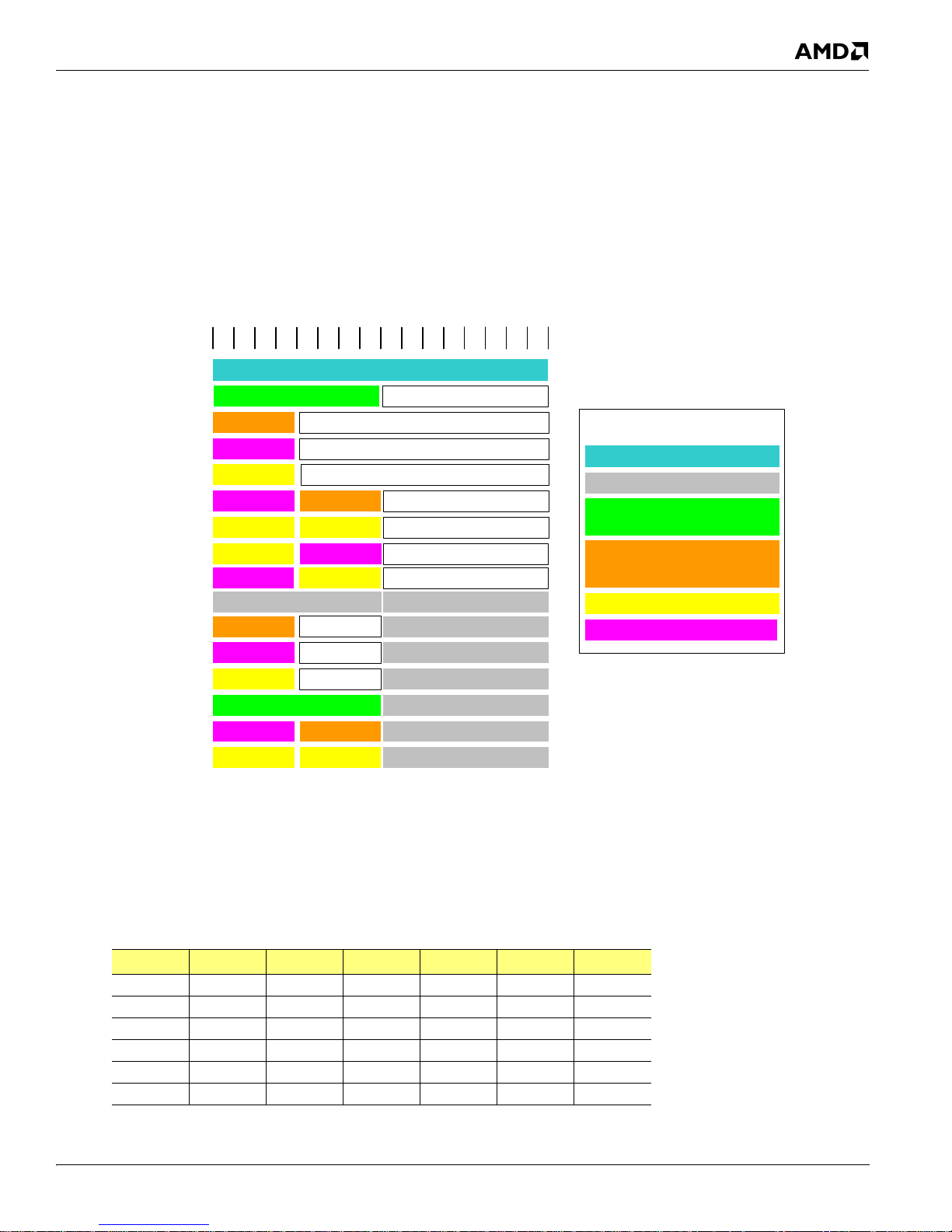
01 32 456789101112131415
PCI-E x16
PCI-E x 8 External Graphics
DL-DVI
PCI-E x 16 External Graphics
TMDS enabling Dual- Link
DVI(DL-DVI)
LEGEND
Not Used
TMDS enabling Single- Link
DVI(SL-DVI)
DisplayPort (DP)
TMDS enabling HDMI
PCI-E x 16 Interface
HDMI
SL-DVI
Not Used
DP
DP
Not Used
SL-DVI Not Used
HDMI Not Used
DP Not Used
DL-DVI
PCI-E x 8
SL-DVIHDMI
PCI-E x 8
PCI-E x 8
DPDP
HDMI Not Used
DP Not Used
SL-DVI Not Used
PCI-E x 8
PCI-E x 8
PCI-E x 8
DP Not Used
DP Not Used
HDMI
HDMI
PCI-E x 8 PCI-E x 8
* Note: Includes dedicated and shared memory. The amount of HyperMemory available is determined by various factors.
For details, please consult your AMD CSS representative.
1.2.4 PCI Express® Interface
Supports PCI-E Gen2 (version 2.0).
•
• Optimized peer-to-peer and general purpose link performance.
• Highly flexible PCI Express implementation to suit a variety of platform needs.
• A dual-port, x16 graphics interface, configurable to any one of the modes illustrated in Figure 1-1:
• Supports programmable lane reversal for the graphics link to ease motherboard layout when the end device does not
© 2009 Advanced Micro Devices, Inc. 45732 AMD 780E Databook 3.10
Proprietary 1-3
support lane reversal.
• Supports six general purpose lanes, for up to six devices on specific ports. Possible configurations are listed in
Table 1-1.
Table 1-1 Possible Configurations for the PCI-E General Purpose Links
GPP1 x4 x4 x2 x2 x2 x1
GPP2-----x1
GPP3 - - x2 x1 x2 x1
GPP4---x1-x1
GPP5 x2 x1 x2 x1 x1 x1
GPP6 - x1 - x1 x1 x1
Figure 1-1 Possible Configurations for the x16 PCI-E Graphics Interface
Config. B Config. C Config. C2 Config. E Config. K Config. L
Page 14

• Supports x1, x2, x4, x8, x12 and x16 polarity inversion.
1.2.5 A-Link Express II Interface
One x4 A-Link Express II interface for connection to an AMD Southbridge. The A-Link Express II is a proprietary
•
interface developed by AMD basing on the PCI Express Gen2 version 2.0 technology, with additional
Northbridge-Southbridge messaging functionalities.
• Supports programmable lane reversal to ease motherboard layout.
1.2.6 2D Acceleration Features
•
Highly-optimized 128-bit engine, capable of processing multiple pixels per clock.
• Hardware acceleration of Bitblt, line drawing, polygon and rectangle fills, bit masking, monochrome expansion,
panning and scrolling, scissoring, and full ROP support (including ROP3).
• Optimized handling of fonts and text using AMD proprietary techniques.
• Game acceleration including support for Microsoft's DirectDraw
Blit, and Masked Blit.
• Acceleration in 1/8/15/16/32-bpp modes:
• Pseudocolor mode for 8bpp
• ARGB1555 and RGB565 modes for 16bpp
• ARGB8888 mode for 32bpp
• Significant increase in the High-End Graphics WinBench
• Setup of 2D polygons and lines.
• Support for GDI extensions:
• In Windows XP and Windows Vista: Alpha BLT, Transparent BLT, and Gradient Fill.
RS780E Features
®
: Double Buffering, Virtual Sprites, Transparent
®
score due to capability for C18 color expansion.
• In Windows 7: Alpha BLT, Transparent BLT, Color Fill BLT, Stretch BLT, and Clear Type BLT.
• Hardware cursor (up to 64x64x32bpp), with alpha channel for direct support of Windows XP, Windows Vista
and Windows 7 alpha cursor.
1.2.7 3D Acceleration Features
•
Fully DirectX 10.0 compliant, including full speed 32-bit floating point per component operations
• Shader Model 4.0 geometry and pixel support in a unified shader architecture:
• Full speed 32-bit floating point processing per component.
• High dynamic range rendering with floating point blending, texture filtering and anti-aliasing support.
• High performance dynamic branching and flow control.
• Nearly unlimited shader instruction store, using an advance caching system.
• Advanced shader design, with ultra-threading sequencer for high efficiency operations.
• Advanced, high performance branching support, including static and dynamic branching.
• 32-bit floating point components for high dynamic range computations.
• Full anti-aliasing on render surfaces up to and including 128-bit floating point formats.
• Support for OpenGL
®
2.0
• Anti-Aliasing Filtering:
• 2x/4x/8x modes.
• Sparse multi-sample algorithm with gamma correction, programmable sample patterns, and centroid sampling.
• Temporal anti-aliasing.
• Adaptive anti-aliasing mode.
• Lossless color compression (up to 8:1) at all resolutions, up to and including widescreen HDTV.
• Anisotropic Filtering:
45732 AMD 780E Databook 3.10 © 2009 Advanced Micro Devices, Inc.
1-4 Proprietary
Page 15

RS780E Features
• 2x/4x/8x/16x modes
• Up to 128-tap texture filtering.
• Adaptive algorithm with performance (bi-linear) and quality (tri-linear) options.
• Improved quality mode due to improved subpixel precision, higher precision LOD computations, and
• Advanced Texture Compression (3Dc+™ ):
• High quality 4:1 compression for normal maps and luminance maps.
• Works with any single-channel or two-channel data format.
• HW support to overcome "Small batch" issues in CPU limited applications.
• 3D resources virtualized to a 32-bit addressing space, for support of large numbers of render targets and textures.
• New vertex cache and vertex fetch design, to increase vertex throughput from previous generations.
• Full support of 64-bit and 128-bit textures and surfaces, which can be 4x to 8x faster than previous generation of HW.
• Up to 8K x 8K textures, including 128 bpp texture are supported.
• New multi-level texture cache to give optimal performance, greater than 8x the previous designs.
• High efficiency ring bus memory controller:
• Programmable arbitration logic maximizes memory efficiency, software upgradeable.
• Fully associative texture, color, and Z cache design.
• New hierarchical Z and stencil buffers with early Z Test.
• New lossless Z-buffer compression for both Z and stencil.
• Fast Z-Buffer Clear.
• Z cache optimized for real-time shadow rendering.
• Z and color compression resources virtualized to a 32-bit addressing space, for support of multiple render targets
rotationally invariant LOD computations.
and textures simultaneously.
1.2.8 Motion Video Acceleration Features
Video scaling and fully programmable YCrCb to RGB color space conversion for full-speed video playback and fully
•
adjustable color controls.
• Adaptive de-interlacing eliminates video artifacts caused by displaying interlaced video on non-interlaced displays,
and by analyzing image and using optimal de-interlacing function on a per-pixel basis.
• Motion video acceleration for HD DVD/Blu-ray technology.
• Dedicated UVD (Unified Video Decoder) hardware for H.264,VC-1, and MPEG-2 decode:
• H.264 implementation is based on the ISO/IEC 14496-10 spec.
• VC-1 implementation is based on the SMPTE 421M spec.
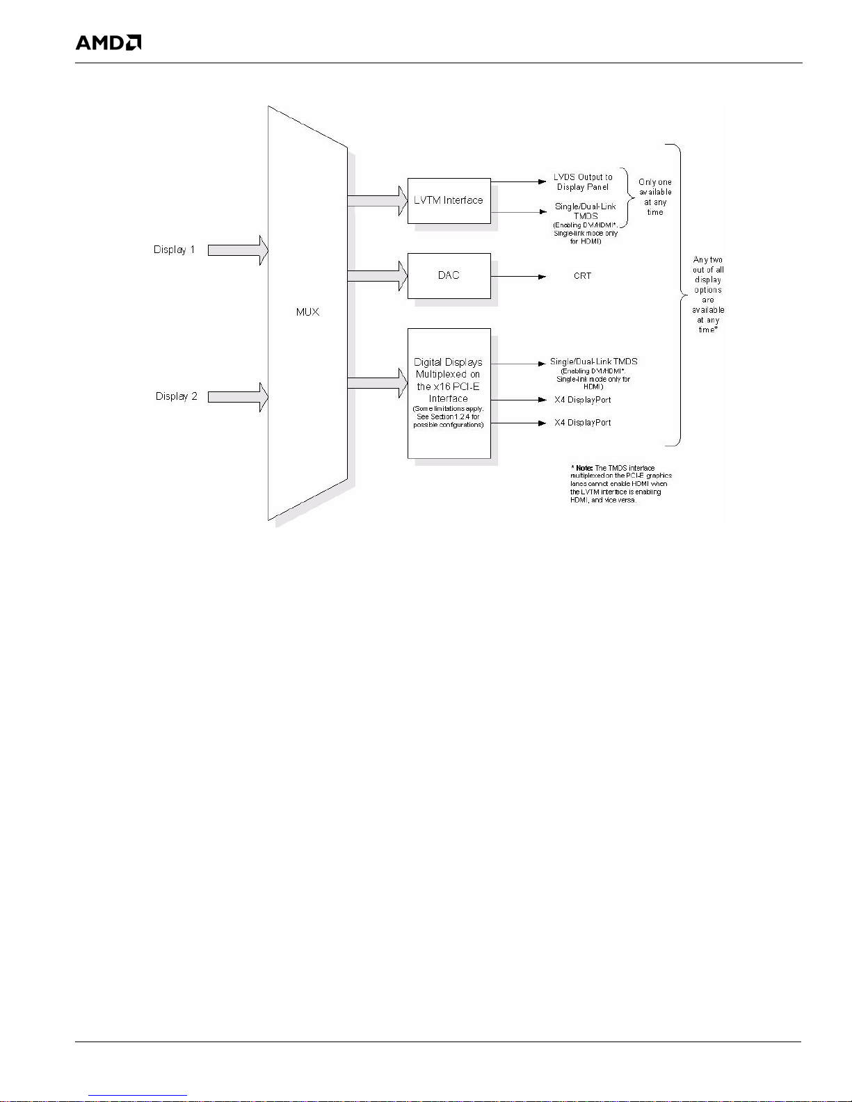
1.2.9 Multiple Display Features
General
• Dual independent displays. Possible configurations are illustrated in Figure 1-2.
© 2009 Advanced Micro Devices, Inc. 45732 AMD 780E Databook 3.10
Proprietary 1-5
Page 16
RS780E Features
Figure 1-2 RS780E Multiple Display Options
• Resolution, refresh rates, and display data can be completely independent for the two display paths.
• Each display controller supports true 30 bits per pixel throughout the display pipe.
• Each display path supports VGA and accelerated modes, video overlay, hardware cursor, hardware icon, and palette
gamma correction.
• Supports both interlaced and non-interlaced displays.
• Full ratiometric expansion ability is supported for source desktop modes up to 1920 pixels/line.
• Maximum DAC frequency of 400 MHz.
• Supports 8, 16, 32, and 64-bpp depths for the main graphics layer:
• For 32-bpp depth, supports xRGB 8:8:8:8, xRGB 2:10:10:10, sCrYCb 8:8:8:8, and xCrYCb 2:10:10:10 data
formats.
• For 64-bpp depth, supports xRGB 16:16:16:16 data format.
• Independent gamma, color conversion and correction controls for main graphics layer.
• Support for DDC1 and DDC2B+ for plug and play monitors.
• 8-bit alpha blending of graphics and video overlay.
• Hardware cursor up to 64x64 pixels in 2 bpp, full color AND/XOR mix, and full color 8-bit alpha blend.
• Hardware icon up to 128x128 pixels in 2 bpp, with two colors, transparent, and inverse transparent. AND/XOR
mixing. Supports 2x2 icon magnification.
• Virtual desktop support.
• Support for flat panel displays via VGA.
• Configurable to support flat panel displays or TVs via DVI/HDMI.
• Integrated HD audio controller for HDMI audio data.
45732 AMD 780E Databook 3.10 © 2009 Advanced Micro Devices, Inc.
1-6 Proprietary
Page 17

RS780E Features
VGA Output
• Maximum resolutions supported by the VGA output for different refresh rates are:
• 2048x1536 @85Hz (pixel clock at 388.5MHz) for 4:3 format
• 2560x1440 @75Hz (pixel clock at 397.25MHz) for 16:9 format
• 2456x1536 @60Hz (pixel clock at 320MHz) for 16:10 format
1.2.10 Integrated LVDS/TMDS (LVTM) Interface
Configurable to output either LVDS or TMDS signals.
•
• LVDS mode:
• Integrated dual-link 18-/24-bit LVDS interface.
• 805 Mbps/channel with 115 MHz pixel clock rate per link (230 MHz maximum pixel clock).
• FPDI-2 compliant; compatible with receivers from National Semiconductor, Texas Instruments, and THine.
• OpenLDI compliant excluding DC balancing.
• Programmable internal spread spectrum controller for the signals.
• TMDS Mode, enabling DVI or HDMI™:
• See Section 1.2.11, “DVI/HDMI™,” for details.
1.2.11 DVI/HDMI™
• Supports two TMDS interfaces, one multiplexed on the PCI-E graphics interface and the other on the LVTM
interface, enabling DVI or HDMI™*
• 1620 Mbps/channel with 162 MHz pixel clock rate per link.
• Supports industry standard EIA-861B video modes including 480p, 720p, 1080i, and 1080p (for a full list of currently
supported modes, contact you AMD CSS representative). Maximum resolutions supported by various modes are:
• Single-link DVI: 1600x1200 @60Hz with standard timings, and 1920x1200 @60Hz with reduced blanking
timings.
• Dual-link DVI: 2560x1600 @60Hz.
• HDMI: 1080p.
• Supports YCbCr 4:4:4 and 4:2:2 modes with HDMI.
• HDMI basic audio support at 32, 44.1 or 48 kHz. Supports two-channel uncompressed audio data, and, for Windows
Vista platforms only, 5.1-channel audio data and DTS. HD audio device compatible with the Microsoft HD audio
driver.
• HDCP support for two independent display streams with on-chip key storage. Also available when the TMDS
interfaces run in dual-link mode.**
Notes: * HDMI must only be enabled on systems that are legally entitled. It is the responsibility of the system designer to
ensure that the system is entitled to support this feature.
§
CEC is not supported.
‡ The TMDS interface multiplexed on the PCI-E graphics lanes cannot enable HDMI when the LVTM interface is
enabling HDMI, and vice versa.
§
(passing HDMI CTS v1.3b). ‡
** HDCP content protection is only available to licensed buyers of the technology and can only be enabled when
connected to an HDCP-capable receiver.
1.2.12 DisplayPort™ Interface
•
Supports all mandatory features of DisplayPort™ Standard, Version 1.1, plus the following optional features:
• 10-bit support.
© 2009 Advanced Micro Devices, Inc. 45732 AMD 780E Databook 3.10
Proprietary 1-7
Page 18

• YCbCr 4:4:4 and 4:2:2 support.
• HDCP support
• Optional test pattern support.
• Supports two independent displays over the PCI-E interface for external graphics (see Figure 1-1,“Possible
Configurations for the x16 PCI-E Graphics Interface,” on page 1-3 for details).
• Supports 4, 2, or 1-lane transmission.
• Supports both the 2.7Gbps and 1.62Gbps link symbol rates.
• Supports the Auxiliary Channel (AUX CH).
• Supports a maximum resolution of 2560x1600 @60Hz with 4 lanes.
1.2.13 Integrated HD Audio Controller and Codec
•
Integrated HD Audio codec supports linear PCM and AC3 (5.1) audio formats for HDMI output.
• Separate logical chip function.
• Can encrypt data onto one associated HDMI output.
• Uses Microsoft UAA driver.
• Internally connected to the integrated HDMI, or HDMI-enabled interface, hence no external cable required.
• Support for basic audio (32, 44.1 or 48 KHz stereo) and AC3 or DTS at the same sample rates.
RS780E Features
1.2.14 Clock Generation
Support for an external clock chip to generate side-port memory, PCI-E, and A-Link Express II clocks.
•
1.2.15 Power Management Features
•
Single chip solution in 55nm, 1.1V CMOS technology.
• Supports ACPI 2.0 for S0, S3, S4, and S5 states.
• Full IAPC (Instantly Available PC) power management support.
• Static and dynamic power management support (APM as well as ACPI) with full VESA DPM and Energy Star
compliance.
• The Chip Power Management Support logic supports four device power states defined for the OnNow Architecture—
On, Standby, Suspend, and Off. Each power state can be achieved by software control bits.
• Hardware controlled intelligent clock gating enables clocks only to active functional blocks, and is completely
transparent to software.
• Dynamic self-refresh for the side-port memory.
• Support for Cool'n'Quiet™ via FID/VID change.
• Support for AMD PowerNow!™.
• Clocks to every major functional block are controlled by a unique dynamic clock switching technique that is
completely transparent to the software. By turning off the clock to the block that is idle or not used at that point, the
power consumption is significantly reduced during normal operation.
• Supports PowerExpress™ and PowerPlay™ (enhanced with the PowerShift™ feature).
• Supports dynamic lane reduction for the PCI-E graphics interface when coupled with an AMD-based graphics
device, adjusting lane width according to required bandwidth.
1.2.16 PC Design Guide Compliance
The RS780E complies with all relevant Windows Logo Program (WLP) requirements from Microsoft for WHQL
certification.
45732 AMD 780E Databook 3.10 © 2009 Advanced Micro Devices, Inc.
1-8 Proprietary
Page 19

Software Features
1.2.17 Test Capability Features
The RS780E has a variety of test modes and capabilities that provide a very high fault coverage and low DPM (Defect Per
Million) ratio:
• Full scan implementation on the digital core logic through ATPG (Automatic Test Pattern Generation Vectors).
• Dedicated test logic for the on-chip custom memory macros to provide complete coverage on these modules.
• A JTAG test mode to allow board level testing of neighboring devices.
• An EXOR tree test mode on all the digital I/O's to allow for proper soldering verification at the board level.
• A VOH/VOL test mode on all digital I/O’s to allow for proper verification of output high and output low values at the
board level.
• Access to the analog modules to allow full evaluation and characterization.
• IDDQ mode support to allow chip evaluation through current leakage measurements.
These test modes can be accessed through the settings on the instruction register of the JTAG circuitry.
1.2.18 Additional Features
•
Integrated spread spectrum PLLs on the memory and LVDS interface.
1.2.19 Packaging
Single chip solution in 55nm, 1.1V low power CMOS technology.
•
• 528-FCBGA package, 21mmx21mm.
1.3 Software Features
• BIOS ability to read EDID 1.1, 1.2, and 1.3.
• Ability to selectively enable and disable several devices including CRT, LCD, and DFP.
• Register-compatible with VGA standards, BIOS-compatible with VESA VBE2.0.
• Supports corporate manageability requirements such as DMI.
• ACPI support.
• Full Write Combining support for maximum performance of the CPU.
• Full-featured, yet simple Windows utilities:
• Calibration utility for WYSIWYG color
• Independent brightness control of desktop and overlay
• End user diagnostics
• Drivers meet Microsoft's rigorous WHQL criteria and are suitable for systems with the "Designed for Windows"
logos.
• Comprehensive OS and API support.
• Hot-key support (Windows ACPI 2.0 or AMD Event Handler Utility where appropriate).
• Extensive power management support.
• Rotation mode support in software.
• Dual CRTC, simultaneous view, extended desktop support (Windows XP and Windows Vista)
• DirectX 10.0 support.
• Switchable overlay support.
• H.264 playback support.
© 2009 Advanced Micro Devices, Inc. 45732 AMD 780E Databook 3.10
Proprietary 1-9
Page 20
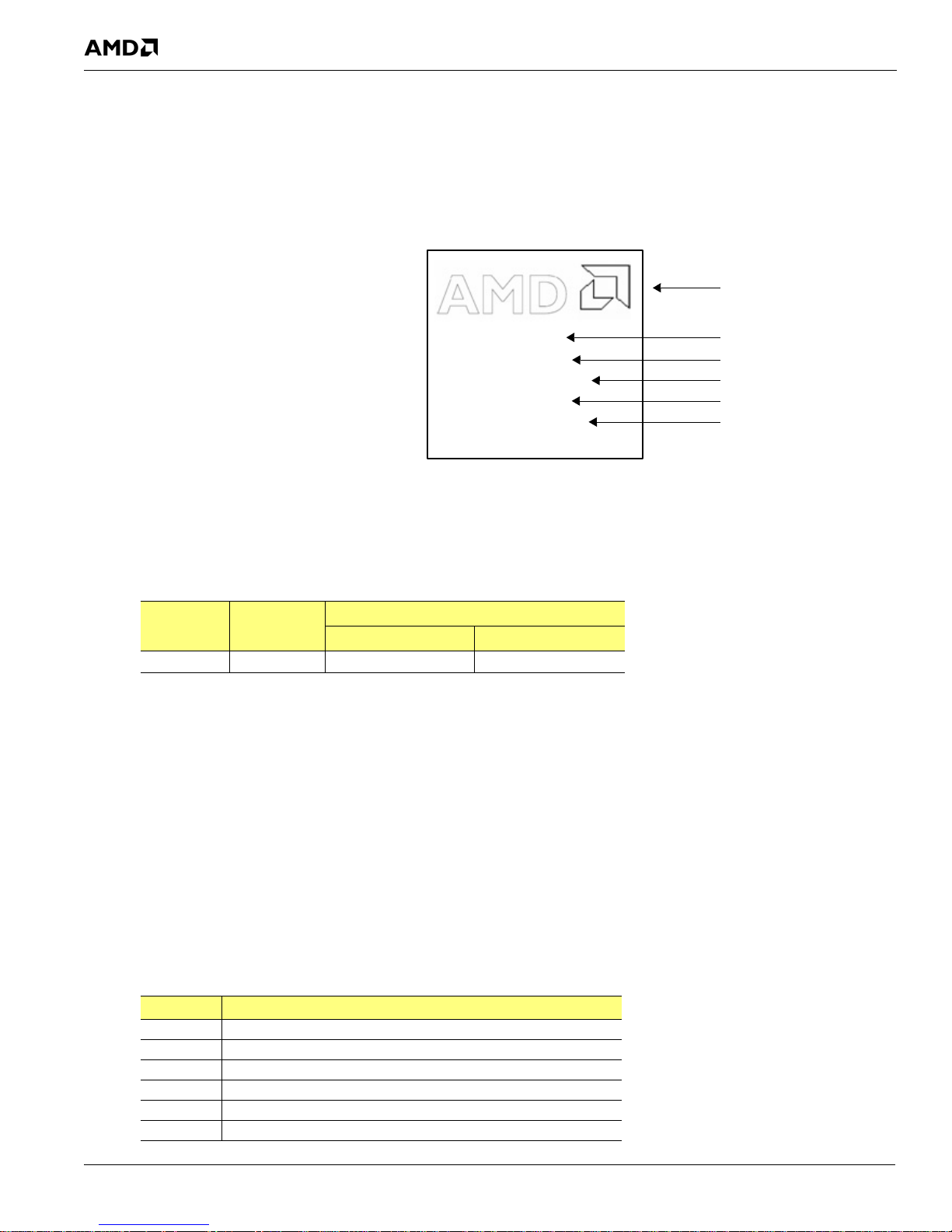
• Supports AMD OverDrive™ utility*.
RADEON IGP
YYWW
MADE IN TAIWAN
WXXXXX
216-0674040
* YY - Assembly Start Year
WW - Assembly Start Week
Part Number
Date Code*
AMD Product Type
AMD Logo
Wafer Lot Number
Country of Origin
*Note: AMD’s product warranty does not cover damages caused by overclocking, even when overclocking is enabled via
the AMD OverDrive utility.
1.4 Branding Diagram
Branding Diagram
Figure 1-3 RS780E ASIC A13 Production Branding
1.5 Graphics Device ID and Graphics Engine Clock Speed
Table 1-2 Graphics Device ID and Graphics Engine Clock Speed
Variant
RS780E 0x9615 200 500
Graphics
Device ID
Graphics Engine Clock Speed (MHz)
Min. Max.
1.6 Conventions and Notations
The following conventions are used throughout this manual.
1.6.1 Pin Names
Pins are identified by their pin names or ball references. Multiplexed pins sometimes assume alternate “functional names”
when they perform their alternate functions, and these “functional names” are given in Chapter 3, “Pin Descriptions and
Strap Options.”
All active-low signals are identified by the suffix ‘#’ in their names (e.g., MEM_RAS#).
1.6.2 Pin Types
The pins are assigned different codes according to their operational characteristics. These codes are listed in Table 1-3.
Table 1-3 Pin Type Codes
Code Pin Type
I Digital Input
O Digital Output
OD Open Drain
I/O Bi-Directional Digital Input or Output
I/OD Digital Input or Open Drain
M Multifunctional
45732 AMD 780E Databook 3.10 © 2009 Advanced Micro Devices, Inc.
1-10 Proprietary
Page 21
Conventions and Notations
Table 1-3 Pin Type Codes (Continued)
Code Pin Type
Pwr Power
Gnd Ground
A-O Analog Output
A-I Analog Input
A-I/O Analog Bi-Directional Input/Output
A-Pwr Analog Power
A-Gnd Analog Ground
Other Pin types not included in any of the categories above
1.6.3 Numeric Representation
Hexadecimal numbers are appended with “h” (Intel assembly-style notation) whenever there is a risk of ambiguity. Other
numbers are in decimal.
Pins of identical functions but different running integers (e.g., “GFX_TX7P, GFX_TX6P,... GFX_TX0P”) are referred to
collectively by specifying their integers in square brackets and with colons (i.e., “GFX_TX[7:0]P”). A similar short-hand
notation is used to indicate bit occupation in a register. For example, NB_COMMAND[15:10] refers to the bit positions
10 through 15 of the NB_COMMAND register.
1.6.4 Register Field
A field of a register is referred to by the format of [Register Name].[Register.Field]. For example,
“NB_MC_CNTL.DISABLE_BYPASS” is the “DISABLE_BYPASS” field of the register “NB_MC_CNTL.”
1.6.5 Hyperlinks
Phrases or sentences in blue italic font are hyperlinks to other parts of the manual. Users of the PDF version of this manual
can click on the links to go directly to the referenced sections, tables, or figures.
1.6.6 Acronyms and Abbreviations
The following is a list of the acronyms and abbreviations used in this manual.
Table 1-4 Acronyms and Abbreviations
Acronym Full Expression
ACPI Advanced Configuration and Power Interface
A-Link-E II A-Link Express II interface between the IGP and the Southbridge.
BGA Ball Grid Array
BIOS
BIST Built In Self Test.
BLT Blit
bpp bits per pixel
CEC Consumer Electronic Control
CPIS Common Panel Interface Specification
CRT Cathode Ray Tube
CSP Chip Scale Package
DAC Digital to Analog Converter
DBI Dynamic Bus Inversion
DDC
DDR Double Data Rate
Basic Input Output System. Initialization code stored in a ROM or Flash RAM used to start up a
system or expansion card.
Display Data Channel. A VESA standard for communicating between a computer system and
attached display devices.
© 2009 Advanced Micro Devices, Inc. 45732 AMD 780E Databook 3.10
Proprietary 1-11
Page 22
Table 1-4 Acronyms and Abbreviations (Continued)
Acronym Full Expression
DFP Digital Flat Panel. Monitor connection standard from VESA.
DPM Defects per Million
DTV Digital TV
DVD Digital Video Disc
DVI
DVS Digital Video Stream
EPROM Erasable Programmable Read Only Memory
FIFO First In, First Out
FPDI Flat Panel Display Interface
GDI Graphics Device Interface
GND Ground
GPIO General Purpose Input/Output
HDCP High-Bandwidth Digital Content Protection
HDMI High Definition Multimedia Interface
HDTV High Definition TV. The 1920x1080 and the 1280x720 modes defined by ATSC.
HPD Hot Plug Detect
iDCT inverse Discrete Cosine Transform
IDDQ Direct Drain Quiescent Current
IGP
JTAG Joint Test Access Group. An IEEE standard.
LVDS Low Voltage Differential Signaling
MB Mega Byte
MPEG
NTSC
PAL Phase Alternate Line. The standard definition TV system used in Europe and other areas.
PCI Peripheral Component Interface
PCI-E PCI Express
PCMCIA
PLL Phase Locked Loop
POST Power On Self Test
PD Pull-down Resistor
PU Pull-up Resistor
ROP Raster Operation
SDRAM Synchronous Dynamic RAM
TMDS Transition Minimized Differential Signaling
UMA Unified Memory Architecture
UV Chrominance (also CrCb). Corresponds to the color of a pixel.
UVD Unified Video Decoder
UXGA Ultra Extended Graphics Array
VBI Vertical Blank Interval
VESA Video Electronics Standards Association
VGA Video Graphics Adapter
VRM Voltage Regulation Module
Digital Video Interface. Monitor connection standard from the DDWG (Digital Display Work
Group).
Integrated Graphics Processor. A single device that integrates a graphics processor and a
system controller.
Motion Pictures Experts Group. Refers to compressed video image streams in either MPEG-1
or MPEG-2 formats.
National Television Standards Committee. The standard definition TV system used in North
America and other areas.
Personal Computer Memory Card International Association. It is also the name of a standard
for PC peripherals promoted by the Association.
Conventions and Notations
45732 AMD 780E Databook 3.10 © 2009 Advanced Micro Devices, Inc.
1-12 Proprietary
Page 23
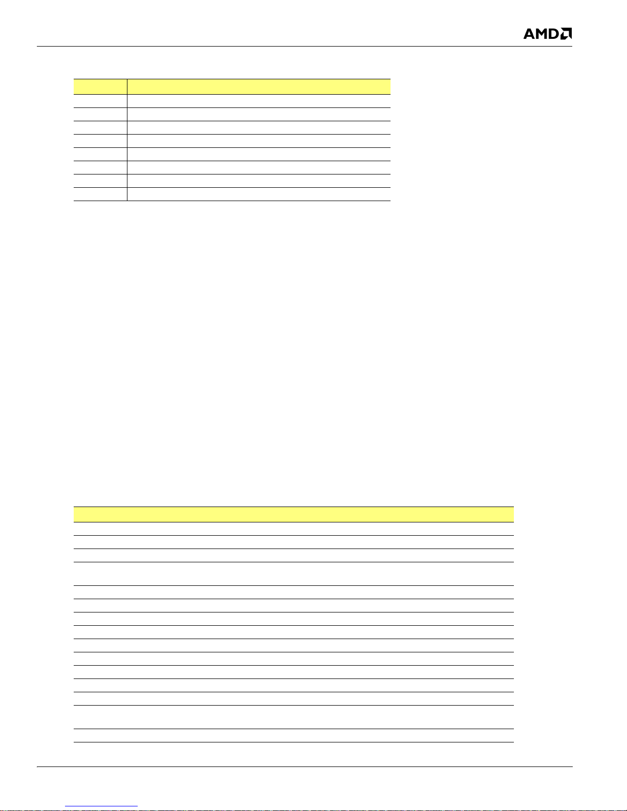
Chapter 2
HyperTransport™
Unit
CPU
Interface
Register Interface
UVD
Setup
Engine2DEngine
3D
Engine
Overlay
Root
MUX
Display 1& 2
CRT
Memory Controller
AMD CPU
Bus Interface
Complex
Optional 16-bit
DDR2/DDR3
Memory Channel
TMDS, enabling DVI/HDMI™
SB
External
Graphics
A-Link-E II
Gfx Interface*
PCI-E
Interface
(1x16 or 2x8
GPP Interface
PCI-E
(6 x 1 Lanes)
Expansion
Slots or
On-board
Devices
(1 x 4 Lanes)
DisplayPort™
(Multiplexed on PCI-E Gfx Lanes)
(Multiplexed on PCI-E Gfx Lanes)
LVDS
TMDS, supporting DVI/HDMI
(Multiplexed on the LVTM interface)
Lanes)
Functional Descriptions
This chapter describes the functional operation of the major interfaces of the RS780E system logic. Figure 2-1, “RS780E
Internal Block Diagram,” illustrates the RS780E internal blocks and interfaces.
2.1 Host Interface
The RS780E is optimized to interface with AMD processors through the HyperTransport
presents an overview of the HyperTransport
Figure 2-1 RS780E Internal Block Diagram
interface. For a detailed description of the interface, please refer to the
TM
interface. This section
© 2009 Advanced Micro Devices, Inc. 45732 AMD 780E Databook 3.10
Proprietary 2-1
Page 24
Host Interface
HT Interface to CPU (PHY)
Configuration
Registers
Root Complex
Memory Controller
LTA
LRA
SCH
Data Link Layer
Protocol/Transaction Layer
HyperTransport I/O Link Specification from the HyperTransport Consortium. Figure 2-2, “Host Interface Block
Diagram,” illustrates the basic blocks of the host bus interface of the RS780E.
Figure 2-2 Host Interface Block Diagram
The HyperTransport (HT) Interface, formerly known as the LDT (Lightning Data Transport) interface, is a high speed,
packet-based link implemented on two unidirectional buses. It is a point-to-point interface where data can flow both
upstream and downstream at the same time. The commands, addresses, and data travel in packets on the HyperTransport
link. Lengths of packets are in multiples of four bytes. The HT link consists of three parts: the physical layer (PHY), the
data link layer, and the protocol/transaction layer. The PHY is the physical interface between the RS780E and the CPU.
The data link layer includes the initialization and configuration sequences, periodic redundancy checks,
connect/disconnect sequences, and information packet flow controls. The protocol layer is responsible for maintaining
strict ordering rules defined by the HT protocol.
The RS780E HyperTransport bus interface consists of eighteen unidirectional differential data/control pairs and two
differential clock pairs in each of the upstream and downstream direction. On power up, the HT link is 8-bit wide and runs
at a default speed of 400MT/s. After negotiation, carried out by the HW and SW together, the link width can be brought
up to 16-bit and the interface can run up to 4.4GT/s. The interface is illustrated in Figure 2-3, “RS780E Host Bus
Interface Signals.” The signal name and direction for each signal is shown with respect to the processor. Note that the
signal names may be different from those used in the pin listing of the RS780E. Detailed descriptions of the signals are
given in section 3.3, “CPU HyperTransport™ Interface‚’ on page 3-5.
45732 AMD 780E Databook 3.10 © 2009 Advanced Micro Devices, Inc.
2-2 Proprietary
Page 25

Side-Port Memory Interface
HT_RXCADN
2
2
RS780E
CPU
HT_TXCALP
HT_RXCALN
HT_RXCALP
HT_TXCALN
HT_RXCADP
HT_RXCTLN
HT_RXCTLP
HT_RXCLKN
HT_RXCLKP
16
16
HT_TXCADN
2
2
HT_TXCADP
HT_TXCTLN
HT_TXCTLP
HT_TXCLKN
HT_TXCLKP
16
16
2
2
2
2
Figure 2-3 RS780E Host Bus Interface Signals
2.2 Side-Port Memory Interface
In order to significantly decrease system power and increase graphics performance, the RS780E provides an optional
side-port memory interface for dedicated frame buffer memory, to be used exclusively for the integrated graphics core.
The side-port memory interface can significantly reduce system power by allowing the CPU to stay in its lowest power
state during periods of inactivity. Screen refreshes are fetched from the side-port memory, and there is no need to "wake
up" the CPU to fetch screen refresh data.
The RS780E memory controller is unique and highly optimized. It operates in 16-bit mode at very high speed (up to
DDR2-800 and DDR3-800, and up to DDR3-1200 when the core voltage is fixed at 1.1V), and has a programmable
interleaved mode that significantly increases the memory bandwidth and reduces data latency to the integrated graphics
core. The additional bandwidth provided to the internal graphics core will also aid the RS780E in reaching and exceeding
Microsoft's Windows Vista
2.2.1 DDR2 Memory Interface
Figure 2-4, “RS780E Side-Port Memory Interface,” on page 2-4 illustrates the side-port memory interface of the
RS780E.
The RS780E memory controller supports up to 128MB of dedicated side-port frame buffer DDR2 memory. It controls a
single rank of DDR2 devices in 16-bit memory configuration. It supports device sizes of 256, 512, and 1024 Mbits, and a
device width of x16. Because the memory controller supplies only one chip select signal, only devices with one chip
select are supported. A wide range of DDR2 timing parameters, configurations, and loadings are programmable via the
RS780E memory controller configuration registers
®
Premium logo requirements.
© 2009 Advanced Micro Devices, Inc. 45732 AMD 780E Databook 3.10
Proprietary 2-3
Page 26
Data Mask MEM_DM[1:0]
Data MEM_DQ[15:0]
2
4
16
RS780E Side-Port Memory
Interface
Data Strobes MEM_DQS[1:0]P/N
Un-buffered DDR2 SDRAM
MEM_CKE, MEM_RAS#,
Differential Clocks MEM_CKP/MEM_CKN
4
2
MEM_CAS#, MEM_WE#
14
Address MEM_A[13:0]
1
Chip Select MEM_CS#
1
On-Die Termination MEM_ODT
3
Bank Address MEM_BA[2:0]
MEM_CALN
MEM_CALP
VDD_MEM
Side-Port Memory Interface
Figure 2-4 RS780E Side-Port Memory Interface
2.2.1.1 Supported DDR2 Components
The memory controller supports DDR2 SDRAM chips in several configurations. These chips are organized in banks,
rows (or pages), and columns. The supported DDR2 components have four or eight banks. Table 2-1 lists the supported
memory components.
Table 2-1 Supported DDR2 Components
DDR2 SDRAM
Config Mbits CS Mode Bank Bits Row Bits Col Bits
16Mbx16 256 4 2 13 9 32
32Mbx16 512 10 2 13 10 64
64Mbx16 1024 11 3 13 10 128
Mbytes
2.2.1.2 Row and Column Addressing
Table 2-2 shows how the physical address P (after taking out the bank bit) is used to provide the row and column
addressing for each size of DDR2 memories.
Table 2-2 DDR2 Memory Row and Column Addressing
Row P10 P14 P13 P12 P11 P22 P21 P20 P19 P18 P17 P16 P15
Column - - PC - P9P8P7P6P5P4P3 P2 P1
Row P23 P14 P13 P12 P11 P22 P21 P20 P19 P18 P17 P16 P15
Column - - PCP10P9P8P7P6P5P4P3 P2 P1
A13 A12 A11 A10 A9 A8 A7 A6 A5 A4 A3 A2 A1 A0
16Mbx16 devices
32Mbx16 devices
Address
45732 AMD 780E Databook 3.10 © 2009 Advanced Micro Devices, Inc.
2-4 Proprietary
Page 27
Side-Port Memory Interface
A13 A12 A11 A10 A9 A8 A7 A6 A5 A4 A3 A2 A1 A0
Row
Column
Row
Column
Note: PC = precharge flag
P23 P14 P13 P12 P11 P22 P21 P20 P19 P18 P17 P16 P15
- - PC P10 P9 P8 P7 P6 P5 P4 P3 P2 P1
P24 P23 P14 P13 P12 P11 P22 P21 P20 P19 P18 P17 P16 P15
- - PC P10 P9 P8 P7 P6 P5 P4 P3 P2 P1
2.2.2 DDR3 Memory Interface
The RS780E memory controller supports up to 128MB of dedicated side-port frame buffer DDR3 memory. It supports a
single rank of DDR3 device in 16-bit memory configuration. It supports device sizes of 512 and 1024 Mbits, and a device
width of x16. A wide range of DDR3 timing parameters, configurations, and loadings are programmable via the RS780E
memory controller configuration registers.
2.2.2.1 Supported DDR3 Components
The memory controller supports DDR3 SDRAM chips in several configurations. These chips are organized in banks,
rows (or pages), and columns. Table 2-3 lists the supported memory components.
Address
64Mbx16 devices
128Mbx16 devices
Table 2-3 Supported DDR3 Components
DDR3 SDRAM
Config Mbits CS Mode Bank Bits Row Bits Col Bits
32Mbx16 512 9 3 12 10 64
64Mbx16 1024 11 3 13 10 128
Mbytes
2.2.2.2 Row and Column Addressing
Table 2-4 shows how the physical address P (after taking out the bank bit) is used to provide the row and column
addressing for each size of DDR3 memories.
Table 2-4 DDR3 Memory Row and Column Addressing
Address
A13 A12 A11 A10 A9 A8 A7 A6 A5 A4 A3 A2 A1 A0
32Mbx16 devices
Row P23 P14 P13 P12 P11 P22 P21 P20 P19 P18 P17 P16 P15
Column - - PCP10P9P8P7P6P5P4P3 P2 P1
64Mbx16 devices
Row P23 P14 P13 P12 P11 P22 P21 P20 P19 P18 P17 P16 P15
Column - - PC P10 P9 P8 P7 P6 P5 P4 P3 P2 P1
Note: PC = precharge flag
© 2009 Advanced Micro Devices, Inc. 45732 AMD 780E Databook 3.10
Proprietary 2-5
Page 28
2.3 LVTM (LVDS/TMDS) Interface
TXOUT_U0N/P
TXOUT_U1N/P
TXOUT_U2N/P
TXCLK_LN/P
TXOUT_L0N/P
TXCLK_UN/P
TXOUT_L1N/P
TXOUT_L2N/P
LVDS_DIGON
LVDS_BLON
LVDS_BLEN
LVDS upper data channel 0
LVDS upper data channel 2
LVDS lower clock channel
LVDS lower data channel 0
LVDS upper clock channel
LVDS lower data channel 1
LVDS lower data channel 2
LVDS_DIGON
LVDS_BLON
LVDS_BLEN
LVDS upper data channel 3
TXOUT_U3N/P
LVDS upper data channel 1
TXOUT_U0N/P
TXOUT_U1N/P
TXOUT_U2N/P
TXCLK_LN/P
TXOUT_L0N/P
TXCLK_UN/P
TXOUT_L1N/P
TXOUT_L2N/P
LVDS_DIGON
LVDS_BLON
LVDS_BLEN
TMDS data channel 0
TMDS data channel 2
NC
TMDS data channel 4
TMDS clock channel
TMDS data channel 5
NC
GPIO3
GPIO2
GPIO4
TMDS data channel 3
TXOUT_U3N/P
TMDS data channel 1
TXOUT_L3N/P
LVDS lower data channel 3
TXOUT_L3N/P
NC
LVTM Interface in LVDS Mode
LVTM Interface in TMDS Mode
The RS780E’s LVTM (LVDS/TMDS) interface supports either an LVDS or a TMDS output. A custom video BIOS from
AMD will configure the LVTM interface to drive out either LVDS or a TMDS signals as desired.
A custom video BIOS and proper signal routing from the LVTM interface to a connector are the only requirements for the
RS780E to support either an LVDS or a TMDS output on the LVTM interface. No other register programming is needed
for selecting one option over the other, and customers should not attempt to configure the LVTM port by programming
the RS780E’s registers directly. Figure 2-5, “LVTM Interface of the RS780E,” compares the functions of the pins in
LVDS and TMDS mode. Operations in the LVDS and TMDS mode are explained in section 2.4, “LVDS‚’ on page 2-7,
and section 2.5, “DVI/HDMI™‚’ on page 2-13, respectively.
LVTM (LVDS/TMDS) Interface
Notice that the RS780E can also provide a TMDS output via its TMDS interface that is multiplexed with its PCI Express
graphics link. As a result, the RS780E can provide two digital display outputs using its two on-chip integrated TMDS
transmitters—one through the LVTM interface, and the other through the TMDS interface multiplexed with the PCI-E
graphics interface.
45732 AMD 780E Databook 3.10 © 2009 Advanced Micro Devices, Inc.
2-6 Proprietary
Figure 2-5 LVTM Interface of the RS780E
Page 29
LVDS
LP1C1LP1C2LP1C3
T Cycle
LP1C4LP1C5LP1C6LP1C7
TXOUT_L0-/+
LP2C1LP2C2LP2C3LP2C4LP2C5LP2C6LP2C7
TXOUT_L1-/+
LP3C1LP3C2LP3C3LP3C4LP3C5LP3C6LP3C7
TXOUT_L2-/+
TXCLK_L-/+
UP1C1UP1C2UP1C3
T Cycle
UP1C4UP1C5UP1C6UP1C7
TXOUT_U0-/+
UP2C1UP2C2UP2C3UP2C4UP2C5UP2C6UP2C7
TXOUT_U1-/+
UP3C1UP3C2UP3C3UP3C4UP3C5UP3C6UP3C7
TXOUT_U2-/+
TXCLK_U-/+
2.4 LVDS
The RS780E’s LVTM interface can operate as a dual-channel 18-/24-bit LVDS interface. Notice that for designs
implementing only a single LVDS channel, the LOWER channel of the interface should be used.
2.4.1 LVDS Data Mapping
Figure 2-6 shows the transmission ordering of the LVDS signals for 18-bit transmission on the lower and the upper data
channels. The signal mappings for single and dual channel transmission are shown in Table 2-5 and Table 2-6
respectively.
Figure 2-7 shows the transmission ordering of the LVDS signals for 24-bit transmission on the lower and the upper data
channels. The signal mappings for single and dual channel transmission are shown in Table 2-9 and Table 2-10
respectively.
Figure 2-6 Single/Dual Channel 18-bit LVDS Data Transmission Ordering
© 2009 Advanced Micro Devices, Inc. 45732 AMD 780E Databook 3.10
Proprietary 2-7
Page 30
Table 2-5 LVDS 18-bit TFT Single Pixel per Clock (Single Channel) Signal Mapping
TX Signal 18-bit
LP1C1 R0
LP1C2 R1
LP1C3 R2
LP1C4 R3
LP1C5 R4
LP1C6 R5
LP1C7 G0
LP2C1 G1
LP2C2 G2
LP2C3 G3
LP2C4 G4
LP2C5 G5
LP2C6 B0
LP2C7 B1
LP3C1 B2
LP3C2 B3
LP3C3 B4
LP3C4 B5
LP3C5 HSYNC
LP3C6 VSYNC
LP3C7 ENABLE
LVDS
45732 AMD 780E Databook 3.10 © 2009 Advanced Micro Devices, Inc.
2-8 Proprietary
Page 31
LVDS
LP1C1LP1C2LP1C3
T Cycle
LP1C4LP1C5LP1C6LP1C7
TXOUT_L0-/+
LP2C1LP2C2LP2C3LP2C4LP2C5LP2C6LP2C7
TXOUT_L1-/+
LP3C1LP3C2LP3C3LP3C4LP3C5LP3C6LP3C7
TXOUT_L2-/+
TXCLK_L-/+
LP4C1LP4C2LP4C3LP4C4LP4C5LP4C6LP4C7
TXOUT_L3-/+
Table 2-6 LVDS 18-bit TFT Dual Pixel per Clock (Dual Channel) Signal Mapping
TX Signal 18-bit TX Signal 18-bit
LP1C1 Ro0 UP1C1 Re0
LP1C2 Ro1 UP1C2 Re1
LP1C3 Ro2 UP1C3 Re2
LP1C4 Ro3 UP1C4 Re3
LP1C5 Ro4 UP1C5 Re4
LP1C6 Ro5 UP1C6 Re5
LP1C7 Go0 UP1C7 Ge0
LP2C1 Go1 UP2C1 Ge1
LP2C2 Go2 UP2C2 Ge2
LP2C3 Go3 UP2C3 Ge3
LP2C4 Go4 UP2C4 Ge4
LP2C5 Go5 UP2C5 Ge5
LP2C6 Bo0 UP2C6 Be0
LP2C7 Bo1 UP2C7 Be1
LP3C1 Bo2 UP3C1 Be2
LP3C2 Bo3 UP3C2 Be3
LP3C3 Bo4 UP3C3 Be4
LP3C4 Bo5 UP3C4 Be5
LP3C5 HSYNC UP3C5 (from the register)
LP3C6 VSYNC UP3C6 (from the register)
LP3C7 ENABLE UP3C7 (from the register)
Note: Signal names with letter 'o' mean 'odd' pixel or the first pixel on the panel, and signal names with letter 'e' mean
'even' pixel or the second pixel on the panel.
© 2009 Advanced Micro Devices, Inc. 45732 AMD 780E Databook 3.10
Proprietary 2-9
Page 32
LVDS
UP1C1
UP1C2UP1C3
T Cycle
UP1C4UP1C5UP1C6UP1C7TXOUT_U0-/+
UP2C1
UP2C2UP2C3UP2C4UP2C5UP2C6UP2C7
TXOUT_U1-/+
UP3C1
UP3C2UP3C3UP3C4UP3C5UP3C6UP3C7
TXOUT_U2-/+
TXCLK_U-/+
UP4C1
UP4C2UP4C3UP4C4UP4C5UP4C6UP4C7
TXOUT_U3-/+
Figure 2-7 Single/Dual Channel 24-bit LVDS Data Transmission Ordering
45732 AMD 780E Databook 3.10 © 2009 Advanced Micro Devices, Inc.
2-10 Proprietary
Page 33
LVDS
Table 2-7 LVDS 24-bit TFT Single Pixel per Clock (Single Channel) Signal Mapping
TX Signal 24-bit
LP1C1 R0
LP1C2 R1
LP1C3 R2
LP1C4 R3
LP1C5 R4
LP1C6 R5
LP1C7 G0
LP2C1 G1
LP2C2 G2
LP2C3 G3
LP2C4 G4
LP2C5 G5
LP2C6 B0
LP2C7 B1
LP3C1 B2
LP3C2 B3
LP3C3 B4
LP3C4 B5
LP3C5 HSYNC
LP3C6 VSYNC
LP3C7 ENABLE
LP4C1 R6
LP4C2 R7
LP4C3 G6
LP4C4 G7
LP4C5 B6
LP4C6 B7
LP4C7 Reserved
© 2009 Advanced Micro Devices, Inc. 45732 AMD 780E Databook 3.10
Proprietary 2-11
Page 34
Table 2-8 LVDS 24-bit TFT Dual Pixel per Clock (Dual Channel) Signal Mapping
TX Signal 24-bit TX Signal 24-bit
LP1C1 Ro0 UP1C1 Re0
LP1C2 Ro1 UP1C2 Re1
LP1C3 Ro2 UP1C3 Re2
LP1C4 Ro3 UP1C4 Re3
LP1C5 Ro4 UP1C5 Re4
LP1C6 Ro5 UP1C6 Re5
LP1C7 Go0 UP1C7 Ge0
LP2C1 Go1 UP2C1 Ge1
LP2C2 Go2 UP2C2 Ge2
LP2C3 Go3 UP2C3 Ge3
LP2C4 Go4 UP2C4 Ge4
LP2C5 Go5 UP2C5 Ge5
LP2C6 Bo0 UP2C6 Be0
LP2C7 Bo1 UP2C7 Be1
LP3C1 Bo2 UP3C1 Be2
LP3C2 Bo3 UP3C2 Be3
LP3C3 Bo4 UP3C3 Be4
LP3C4 Bo5 UP3C4 Be5
LP3C5 HSYNC UP3C5 (from the register)
LP3C6 VSYNC UP3C6 (from the register)
LP3C7 ENABLE UP3C7 (from the register)
LP4C1 Ro6 UP4C1 Re6
LP4C2 Ro7 UP4C2 Re7
LP4C3 Go6 UP4C3 Ge6
LP4C4 Go7 UP4C4 Ge7
LP4C5 Bo6 UP4C5 Be6
LP4C6 Bo7 UP4C6 Be7
LP4C7 Reserved UP4C7 Reserved
LVDS
Note: Signal names with letter 'o' mean 'odd' pixel or the first pixel on the panel, and signal names with letter 'e' mean
'even' pixel or the second pixel on the panel.
2.4.2 LVDS Spread Spectrum
The RS780E has an internal LVDS spread spectrum controller capable of generating a frequency modulated profile for
the LVDS signals. The amount of spread (center spread of up to +/-2.5% and down spread of up to 5%) and the
modulation frequency (in the range of 20-50kHz) are programmable through the LVDS registers.
45732 AMD 780E Databook 3.10 © 2009 Advanced Micro Devices, Inc.
2-12 Proprietary
Page 35
DVI/HDMI™
TX0P
TX0M
TX1P
TX1M
TX2P
TX2M
TXCP
TXCM
TG9TG8TG7TG6TG5TG4TG3TG2TG1TG0
Depending upon state of HSYNC and VSYNC
Depending upon encoded Green channel pixel dataDepending upon state of PLL_SYNC and CTL1
Depending upon state of CTL2 and CTL3
TR1TR0 TR2 TR3 TR4 TR5 TR6 TR7 TR8 TR9
Depending upon encoded Red channel pixel data
TB0 TB1 TB2 TB3 TB4 TB5 TB6 TB7 TB8 TB9
Depending upon encoded Blue channel pixel data
Various control and audio (for HDMI only) signals
Various control and audio (for HDMI only) signals
Various control and audio (for HDMI™ only) signals
Encoded Red Channel Pixel Data
Encoded Green Channel Pixel Data
Encoded Blue Channel Pixel Data
2.5 DVI/HDMI™
2.5.1 DVI/HDMI™ Data Transmission Order and Signal Mapping
The RS780E contains two dual-link TMDS interfaces, multiplexed on the PCI Express® graphics lanes (see section 3.9,
“TMDS Interface Multiplexed on the PCI Express® Graphics Lanes‚’ on page 3-10
section 3.8, “LVTM Interface in TMDS Mode‚’ on page 3-9), which support clock frequencies of up to 162 MHz on each
link.
Figure 2-8 shows the transmission ordering of the signals on the interfaces.
) and on the LVTM interface (see
Figure 2-8 Data Transmission Ordering for the TMDS Interfaces
For dual-link mode, which is for DVI only, the same transmission order applies to data channels on the second link, with
the first link transmitting data for even pixels and the second link for odd pixels. See
The signal mapping for the transmission is shown in
Table 2-9 (single link) and Table 2-10 (dual-link DVI) below.
Table 2-10 below for details.
© 2009 Advanced Micro Devices, Inc. 45732 AMD 780E Databook 3.10
Proprietary 2-13
Page 36

Table 2-9 Single Link Signal Mapping for DVI/HDMI™
DVI/HDMI™
DVI/HDMI™
Functional Name
TX0M/P Phase 1 B0
TX1M/P Phase 1 G0
TX2M/P Phase 1 R0
Note: H/VSYNC are transmitted on TX0M/P (Blue) channel during blank.
Data Phase Signal
Phase 2 B1
Phase 3 B2
Phase 4 B3
Phase 5 B4
Phase 6 B5
Phase 7 B6
Phase 8 B7
Phase 9 B8
Phase 10 B9
Phase 2 G1
Phase 3 G2
Phase 4 G3
Phase 5 G4
Phase 6 G5
Phase 7 G6
Phase 8 G7
Phase 9 G8
Phase 10 G9
Phase 2 R1
Phase 3 R2
Phase 4 R3
Phase 5 R4
Phase 6 R5
Phase 7 R6
Phase 8 R7
Phase 9 R8
Phase 10 R9
45732 AMD 780E Databook 3.10 © 2009 Advanced Micro Devices, Inc.
2-14 Proprietary
Page 37

DVI/HDMI™
Table 2-10 Dual-Link Signal Mapping for DVI
DVI Functional
Notes:
- H/VSYNC are transmitted on TX0M/P (Blue) channel during blank.
- For DVI dual-link mode, the first active data pixel is defined as pixel#0 (an even pixel), as opposed to the DVI specifications.
Link 1 Link 2
Name
TX0M/P Phase 1 EVEN_B0 TX3M/P Phase 1 ODD_B0
TX1M/P Phase 1 EVEN_G0 TX4M/P Phase 1 ODD_G0
TX2M/P Phase 1 EVEN_R0 TX5M/P Phase 1 ODD_R0
Data Phase Signal
Phase 2 EVEN_B1 Phase 2 ODD_B1
Phase 3 EVEN_B2 Phase 3 ODD_B2
Phase 4 EVEN_B3 Phase 4 ODD_B3
Phase 5 EVEN_B4 Phase 5 ODD_B4
Phase 6 EVEN_B5 Phase 6 ODD_B5
Phase 7 EVEN_B6 Phase 7 ODD_B6
Phase 8 EVEN_B7 Phase 8 ODD_B7
Phase 9 EVEN_B8 Phase 9 ODD_B8
Phase 10 EVEN_B9 Phase 10 ODD_B9
Phase 2 EVEN_G1 Phase 2 ODD_G1
Phase 3 EVEN_G2 Phase 3 ODD_G2
Phase 4 EVEN_G3 Phase 4 ODD_G3
Phase 5 EVEN_G4 Phase 5 ODD_G4
Phase 6 EVEN_G5 Phase 6 ODD_G5
Phase 7 EVEN_G6 Phase 7 ODD_G6
Phase 8 EVEN_G7 Phase 8 ODD_G7
Phase 9 EVEN_G8 Phase 9 ODD_G8
Phase 10 EVEN_G9 Phase 10 ODD_G9
Phase 2 EVEN_R1 Phase 2 ODD_R1
Phase 3 EVEN_R2 Phase 3 ODD_R2
Phase 4 EVEN_R3 Phase 4 ODD_R3
Phase 5 EVEN_R4 Phase 5 ODD_R4
Phase 6 EVEN_R5 Phase 6 ODD_R5
Phase 7 EVEN_R6 Phase 7 ODD_R6
Phase 8 EVEN_R7 Phase 8 ODD_R7
Phase 9 EVEN_R8 Phase 9 ODD_R8
Phase 10 EVEN_R9 Phase 10 ODD_R9
DVI Functional
Name
Data Phase Signal
© 2009 Advanced Micro Devices, Inc. 45732 AMD 780E Databook 3.10
Proprietary 2-15
Page 38

2.5.2 Support for HDMI™ Packet Types
Table 2-11 Support for HDMI™ Packet Type
DVI/HDMI™
Packet
Value
0x00 Null Yes Inserted by hardware when needed.
0x01
0x02 Audio Sample Yes
0x03 General Control No
0x04 ACP Packet No — —
0x05 ISRC1 Packet No — —
0x06 ISRC2 Packet No — —
0x07 Reserved N/A N/A N/A
InfoFrame Packet Type
HDMI™ IDEIA-861B
0x80 0x00 Vendor-Specific Yes* — —
0x81 0x01 AVI Yes Inserted on line selected by software.
0x82 0x02
0x83 0x03 Audio Yes
0x84 0x04 MPEG Source No —
* Note: These packet types are supported using generic packet types. A maximum of two of them can be supported simultaneously.
Packet Type
Audio Clock
Regeneration
ID
Source Product
Descriptor
Supported
or Not
Yes Inserted by hardware as required. —
Yes * — —
Source Comment
Sent when required to meet
maximum time between data island
specification.
Audio samples come from HD audio DMA.
Channel status from HD audio and video
registers.
Inserted in horizontal blank whenever audio
FIFO contains data.
Sending and contents controlled by video
driver.
For colorimetry, repetition count,
video format, picture formatting.
Inserted on line selected by software.
Contents from registers written by video
and HD audio drivers.
For channel counts, sampling
frequency, etc.
According to the CEA-861
specification, MPEG Source
InfoFrames should not be used.
—
—
45732 AMD 780E Databook 3.10 © 2009 Advanced Micro Devices, Inc.
2-16 Proprietary
Page 39
VGA DAC Characteristics
2.6 VGA DAC Characteristics
Table 2-12 VGA DAC Characteristics
Parameter Min Typ Max Notes
Resolution 10 bits - - 1
Maximum PS/2 setting Output Voltage - 0.7V - 1
Maximum PS/2 setting Output Current - 18.7mA - 1
Full Scale Error +8% / -3% - +10% 2, 3
DAC to DAC Correlation -2% - +2% 1, 4
Differential Linearity -2 LSB - +2 LSB 1, 5
Integral Linearity -2 LSB - +2 LSB 1, 5
Rise Time (10% to 90%) 0.58ns - 1.7ns 1, 6
Full Scale Settling Time - TBA - 1, 7, 8
Glitch Energy - TBA - 1, 8
Monotonicity - - - 9
Notes:
1 - Tested over the operating temperature range at nominal supply voltage, with an Iref of -1.50mA (Iref is the level of the current flowing
out of the RSET resistor).
2 - Tested over the operating temperature range at reduced supply voltage, with an Iref of -1.50mA (Iref is the level of the current flowing
out of the Rset resistor).
3 - Full scale error from the value predicted by the design equations.
4 - About the mid-point of the distribution of the three DACs measured at full scale deflection.
5 - Linearity measured from the best fit line through the DAC characteristics. Monotonicity guaranteed.
6 - Load = 37.5 + 20 pF with Iref = -1.50 mA (Iref is the current flowing out of the Rset resistor).
7 - Measured from the end of the overshoot to the point where the amplitude of the video ringing is down to +/-5% of the final steady state
value.
8 - This parameter is sampled, not 100% tested.
9 - Monotonicity is guaranteed.
© 2009 Advanced Micro Devices, Inc. 45732 AMD 780E Databook 3.10
Proprietary 2-17
Page 40
2.7 DVI-I Support
VGA Signals
The RS780E has the capability of driving both digital and analog outputs simultaneously to a DVI-I connector. This is
accomplished by routing the RED, GREEN, BLUE, DACHSYNC, DACVSYNC, and AVSSN signals from the
RS780E’s CRT output (see
C4(HS), C5(GND), and Pin 8 (VS) signals (see
For the DVI output portion of the DVI-I connector, AMD recommends using the RS780E’s LVTM interface to provide
the DVI output and routing these digital signals (see
appropriate inputs on the DVI-I connector. The video BIOS must be configured so that the RS780E drives out DVI
signals from its LVTM interface. Display modes supported include desktop resolutions such as 800x600, 1024x768,
1152x864, 1280x1024, and 1600x1200 at 16bpp or 32bpp, with 60Hz or 75Hz screen refresh rate.
DVI-I Support
section 3.7, “CRT Interface‚’ on page 3-7) to the DVI-I connector’s C1(R), C2(G), C3(B),
Figure 2-9, “Pins for Analog Output on the DVI-I Connector,” below).
Figure 2-9 Pins for Analog Output on the DVI-I Connector
section 2.3, “LVTM (LVDS/TMDS) Interface‚’ on page 2-6) to the
2.8 Clock Generation
The RS780E provides support for an external clock chip to generate side-port memory, PCI-E, and A-Link II clocks. For
information on the supported external clock chips, please consult your AMD CSS representative.
45732 AMD 780E Databook 3.10 © 2009 Advanced Micro Devices, Inc.
2-18 Proprietary
Page 41

Chapter 3
Pin Descriptions and Strap Options
This chapter gives the pin descriptions and the strap options for the RS780E. To jump to a topic of interest, use the
following list of hyperlinked cross references:
“Pin Assignment Top View” on page 3-2
“Interface Block Diagram” on page 3-4
“CPU HyperTransport™ Interface” on page 3-5
“Side-port Memory Interface” on page 3-5
“PCI Express® Interfaces” on page 3-6:
“1 x 16 or 2 x 8 Lane Interface for External Graphics” on page 3-6
“A-Link Express II Interface for Southbridge” on page 3-6
“6 x 1 Lane Interface for General Purpose External Devices” on page 3-6
“Miscellaneous PCI Express® Signals” on page 3-6
“Clock Interface” on page 3-7
“CRT Interface” on page 3-7
“LVTM Interface” on page 3-8
“TMDS Interface Multiplexed on the PCI Express® Graphics Lanes” on page 3-10
“DisplayPort™ Interface” on page 3-10
“Power Management Pins” on page 3-11
“Miscellaneous Pins” on page 3-12
“Power Pins” on page 3-12
“Ground Pins” on page 3-13
“Strapping Options” on page 3-14
© 2009 Advanced Micro Devices, Inc. 45732 AMD 780E Databook 3.10
Proprietary 3-1
Page 42

3.1 Pin Assignment Top View
3.1.1 RS780E Pin Assignment Top View
The figures below only represent the relative ball positions. For the actual physical layout of the balls, please refer to
Figure 5-2, “RS780E Ball Arrangement (Bottom View),” on page 5- 10.
Pin Assignment Top View
12345678910111213
A
VSSAPCIE GFX_TX 2N GFX_RX1N GFX_TX1N GFX_TX0N VDDPCIE
B
GFX_RX2N GFX_RX2P GFX_TX2P GFX_RX0N VDDPCIE AUX_CAL LDTSTOP#
C
D GFX_TX3P GFX_TX3N VSSAPCIE GFX_RX0P VSSAPCIE VDDPCIE
E
GFX_TX4N GFX_TX4P VSSAPCIE GFX_RX3P VDDPCIE
GFX_TX6P GFX _TX6N GFX_TX 5N GFX_TX5P GFX_RX3N VDDPCIE LV DS_ BLO N DAC_SCL VDD18 REFCLK_N AVDD
F
VSSAPCIE VSSAPCIE VSSAPCIE GFX_RX4P GFX_RX4N VDDPCIE VSS VDD18 RESERVED LVDS_ENA_BL
G
H
GFX_TX8P GFX _TX8N GFX_TX 7N GFX_TX7P GFX_RX5P GFX_RX5N VSSAPCIE VDDPCIE VDDA18PCIE VDD33 VDD33
J
GFX_TX9N GFX_TX9P VSSAPCIE GFX_RX6N GFX_RX6P GFX_RX7P GFX_RX7N VDDPCIE VDDA18PCIE VDDC VSS
GFX_TX11P GFX_TX11N GFX_TX10N GFX_TX10P VDDPCIE VDDA18PCIE VSS VDDC
K
L
VSSAPCIE VSSAPCIE VSSAPCIE GFX_RX8P GFX_RX8N VSSAPCIE GFX_RX9N VDDPCIE VDDA18PCIE VDDC VSS
M
GFX_TX13P GFX_TX13N GFX_TX12N GFX_TX12P GFX_RX11N VSSAPCIE GFX_RX10N GFX_RX9P VDD PCIE VDDA18PCIE VSS VDDC VDDC
GFX_TX14N GFX_TX14P VSSAPCIE VDDC VSS
N
GFX_TX15P GFX_TX15N GFX_RX14N GFX_RX14P GFX_RX11P VSSAPCIE GFX_RX10P GFX_RX12N VDDPCI E VDDA18PCIE VDDC VSS VDDC
P
R
VSSAPCIE VSSAPCIE VSSAPCIE GFX_RX13N GFX_RX13P VSSAPCIE GFX_RX12P VDDPCIE VDDA18PCIE VSS VDDC
GFX_REFCLKNGFX_REFCLK
T
GPP_REFCLKPGPP_REFCLK
U
GPP_TX5P GPP_TX5N
V
VSSAPCIE VSSAPCIE VSSAPCIE SB_RX3P GPP_RX3N VSSAPCIE VSSAPCIE VDDA18PCIE VSS MEM_RAS#
W
GPP_TX3P GPP_TX3N GPP_TX4N GPP_T X4P SB_RX3N VSSAPCIE SB_RX1N SB_RX0N VDDA18PCIE VDD_MEM MEM_CAS#
Y
GPP_TX2N GPP_TX2P VSSAPCIE SB_RX2P SB_RX2N SB_RX1P SB_RX0P VDDA18PCIE VDD_MEM MEM_A4
AA
AB
VSSAPCIE VSSAPCIE GPP_TX1N GPP_ TX1P VSSAPCIE SB_TX2P VSSAPCIE PCE_CALRN VDDA18PCIE VDD_MEM VSS MEM_A0 MEM_CS#
GPP_TX0P GPP_TX0N VSSAPCIE VSSAPCIE SB_TX2N PCE_CALRP VDD_MEM VSS
AC
GPP_RX2P GPP_RX2N GPP_RX1N GPP_RX0N SB_TX 3P SB_TX1N SB_TX0P
AD
VSSAPCIE GPP_RX1P GPP_RX0P VSSAPCIE SB_TX3N SB_TX1P SB_TX0N
AE
VSSAPCIE GFX_RX1P GFX_TX1P GFX_TX0P VDDPCIE
GFX_RX15N GFX_RX 15P VDDPCIE VDDA18PCIE VDDC VSS
P
N
GPPSB_REFC
12345678910111213
VSSAPCIE GPP_RX4P GPP_RX4N GPP_RX5N GPP_RX5P VDDPCIE VDDA18PCIE VSS VDDC
GPPSB_REFC
LKN
GPP_RX3P VSSAPCIE VSSAPCIE VSSAPCIE VDDPCIE MEM_A2 VSS
LKP
DDC_DATA1/
AUX1N
DDC_CLK1/
AUX1P
VDDA18PCIEP
LL
VDDA18PCIEP
LL
DDC_CLK0/
AUX0P
DDC_DATA0/
AUX0N
SYSRESET# TMDS_HPD HPD VSS SUS_STAT# TESTMODE
DAC_SDA LVDS_DIGON REFCLK_P AVD D
THERMALDIO
DE_N
THERMALDIO
DE_P
I2C_DATA
POWERGOOD DAC_HSYNC PLLVDD VDDLTP18
I2C_CLK STRP_DATA DAC_VSYNC PLLVSS VSSLTP18
VDDA18PCIE VDD_MEM VDD18_MEM MEM_COM PN MEM_A8
VDDA18PCIE VDD_MEM VDD18_MEM MEM_COMPP MEM_A11
ALLOW_LDTSTO
P
CPU Interface
A-Link Express II Interface
Clock Interface
Side-port Memory Interface
CRT Interface
External graphics Interface
LVDS Interface
General Purpose External Device Interface
Power Management Interface
Powers
Grounds
Others
Figure 3-1 RS780E Pin Assignment Top View (Left)
45732 AMD 780E Databook 3.10 © 2009 Advanced Micro Devices, Inc.
3-2 Proprietary
Page 43
Pin Assignment Top View
14 15 16 17 18 19 20 21 22 23 24 25
VDDLT33 VDDLT18 TXCLK_LN TXOUT_U1P TXOUT_ U0N TXOUT_L3P TXOUT_L2N TXOUT_L 1P TXOUT_ L0P VDDHTRX HT_RXCALN VSSAHT A
VDDLT33 VDDLT18 TXCLK_LP TXOUT_U1N TXOUT_U0P TXOUT_L3N TXOUT_L2P TX OUT_L1N TXOUT_L0N VDDHTRX HT_TXCALP HT_TX CALN B
VSSLT VS SLT VSSLT VSS LT VSSLT HT_RXCALP HT _REFCLKN HT_RE FCLKP C
PLLVDD18 VSSLT TXCLK_UP TX CLK_UN TXOU T_U3P TXOUT_U3N TXOUT_U2P TXOUT_U2N VDDHTRX VSSAHT HT_TXCAD0P HT_TXCAD0N D
VSS VSS RESERVED GREEN BLUE VSSLT VDDHTRX VSSAHT HT_TXCAD1P HT_TXCAD1N E
AVDDDI RESERVED RESERVED GREEN# BLUE# VDDHTRX HT_TXCAD8P HT_TXCAD3N HT_TXCAD3P HT_TXCAD2P HT_TXCAD2N F
DAC_RSET AVSSDI RED# RED VDDHTRX HT_TXCAD9P HT_TXCAD8N VSSAHT VSSAHT VS SAHT G
AVSS Q AVDDQ VDDA18HTPLL VDDHTRX VS SAHT VSSAHT HT_TXCAD 9N HT_TXCAD4N HT_TXCA D4P HT_TXCLK0P HT_TXCLK 0N H
VDDC VSS VDDC VDDHT HT_TXCAD11P HT_TXCAD12N HT_TXCAD10P HT_TXCAD10N VSSAHT HT_TXCAD5N HT_TXCAD5P J
VSS VDDC VDDHT HT_TXCAD11N HT_TXCAD7N HT_TXCAD7P HT_TXCAD6P HT_TXCAD6N K
VDDC VSS VDDHT VSSAHT HT_TXCAD13N HT_TXCAD12P HT_TXCLK1N HT_TXCLK1P VSSAHT VSSAHT VSSAHT L
VSS VDDC VDDHT VDDHTTX HT_TXCAD 15N HT_TXCAD13P VSSAHT HT_TXCAD14P HT_RXCTL0P HT_RXCTL0N HT_TXCTL0P HT_TXCTL0N M
VDDC VSSAHT HT_RXCAD7P HT_RXCAD7N N
VDDC VSS VDDHT VDDHTTX HT_TXCAD15P HT_TXCTL1P VSSAHT HT_T XCAD14N HT_RXCAD5P HT_RXCAD5N HT_RXCAD6N HT_RXCAD6P P
VSS VDDC VDDHT VDDHTTX HT_TXCTL1N VSSAHT HT_RXCTL1N HT_RXCTL1P VSSAHT VSSAHT VSSAHT R
VDDC VDD C VDDHT VDDHTTX HT_RXCLK0P HT_RXCLK0N HT_RXCAD4N HT_RXCAD4P T
VSS VSS VDDC VDDHTTX
MEM_ODT MEM_CKP MEM_DQ4 VDDHTTX VSSAHT
MEM_CKN VSS MEM_DM0 MEM_DQS0N VDDHTTX
MEM_A13 MEM_DQ7 MEM_DQS0P VSS MEM_DQ3 VDDHTTX VSSAHT HT_RXCAD11P
VSS MEM_DQ 6 ME M_DQ5 MEM_DQ0 MEM_DQ2 MEM_DQ1 VDDHTTX HT_RXCLK1N
MEM_A6 VSS MEM_A5 VSS MEM_CKE VSS MEM_DQ12 VSS VDDHTTX HT_RXCLK1P HT_RXCAD9N HT_RXCAD9P AB
MEM_A12 MEM_A10 MEM_DQ11 MEM_DQ8 MEM_DQ14 VDDHTTX HT_RXCAD8P HT_RXCAD8N AC
MEM_A7 MEM_A9 MEM_BA0 MEM_BA2 MEM_WE# MEM_DQ9 MEM_DQS1P MEM_DQ15 MEM_DQ13 IOPLLVSS VDDHTTX VSSAHT AD
VSS MEM_A3 MEM_A1 MEM_BA1 MEM_VREF MEM_DM1 VSS MEM_DQS1N MEM_DQ10 IOPLLVDD18 IOPLLVDD VDDHTTX AE
14 15 16 17 18 19 20 21 22 23 24 25
HT_RXCAD15 HT_RXCAD15 HT_RXCAD14 HT_RXCAD14
HT_RXCAD13 HT_RXCAD13
HT_RXCAD12 HT_RXCAD12
VSSAHT HT_RXCAD3P HT_RXCAD3N U
HT_RXCAD1P HT_RXCAD1N HT_RXCAD2N HT_RXCAD2P V
VSSAHT VSSAHT VSSAHT W
HT_RXCAD11
HT_RXCAD0N HT_RXCAD0P Y
HT_RXCAD10 HT_RXCAD10
AA
CPU Interface
A-Link Express II Interface
Clock Interface
Side-port Memory Interface
CRT Interface
External graphics Interface
LVDS Interface
General Purpose External Device Interface
Power Management Interface
Powers
Grounds
Others
Figure 3-2 RS780E Pin Assignment Top View (Right)
© 2009 Advanced Micro Devices, Inc. 45732 AMD 780E Databook 3.10
Proprietary 3-3
Page 44

3.2 Interface Block Diagram
HT_RXCAD[15:0]P, HT_RXCAD[15:0]N
HT_RXCLK[1:0]P, HT_RXCLK[1:0]N
HT_RXCTL[1:0]P, HT_RXCTL[1:0]N
HT_TXCTL[1:0]P, HT_TXCTL[1:0]N
HT_RXCALP, HT_RXCALN
HT_TXCALP, HT_TXCALN
HT_TXCLK[1:0]P, HT_TXCLK[1:0]N
HT_TXCAD[15:0]P, HT_TXCAD[15:0]N
SB_TX[3:0]P, SB_TX[3:0]N
SB_RX[3:0]P, SB_RX[3:0]N
TXOUT_U0N, TXOUT_U0P
TXOUT_U1N, TXOUT_U1P
TXOUT_U2N, TXOUT_U2P
TXCLK_LN, TXCLK_LP
TXOUT_L0N, TXOUT_L0P
TXCLK_UN, TXCLK_UP
TXOUT_L1N, TXOUT_L1P
TXOUT_L2N, TXOUT_L2P
GFX_TX[15:0]P, GFX_TX[15:0]N
GFX_RX[15:0]P, GFX_RX[15:0]N
GPPSB_REFCLKP, GPPSB_REFCLKN
AVSSQ
TESTMODE
THERMALDIDOE_N,
SYSRESET#
POWERGOOD
VDDC
PLLVSS
DAC_RSET
RED, RED#
GREEN, GREEN#
DAC_SCL
DAC_SDA
DAC_HSYNC
DAC_VSYNC
BLUE, BLUE#
THERMALDIODE_P
HT
Interface
LVTM
Interface
A-Link Express
II Interface
Power
Management
Interface
Misc. Signals
PCI-E
External
Graphics or
TMDS
Interface
CRT
Interface
Clock
Interface
Power
Grounds
VDDHTRX
AVSSDI
LVDS_DIGON
LVDS_BLON
PCI-E
Interface
for General
Purpose
External
Devices
GPP_TX[5:0]P, GPP_TX[5:0]N
GPP_RX[5:0]P, GPP_RX[5:0]N
PCE_CALRP
Misc. PCI-E
Signals
PCE_CALRN
VSS
HT_REFCLKP, HT_REFCLKN
LDTSTOP#
ALLOW_LDTSTOP
I2C_CLK
DDC_DATA0/AUX0N
I2C_DATA
STRP_DATA
TMDS_HPD
IOPLLVDD
AVDD
AVDDDI
VDDLTP18
VDDLT18
AVDDQ
LVDS_EN_BL
DDC_CLK0/AUX0P
VSSLT
IOPLLVSS
VSSAPCIE
VSSAHT
VDD_MEM
IOPLLVDD18
PLLVDD
PLLVDD18
VDDA18HTPLL
VDD33
VDDHT
VDDA18PCIEPLL
VDDA18PCIE
GFX_REFCLKP, GFX_REFCLKN
VDD18_MEM
VDD18
VDDHTTX
AUX_CAL
DDC_CLK1/AUX1P
HPD
REFCLK_N, REFCLK_P
DDC_DATA1/AUX1N
MEM_DM[1:0]
MEM_A[13:0]
MEM_CKE
MEM_CKP, MEM_CKN
MEM_RAS#
MEM_CS#
Side-port
Memory
Interface
MEM_CAS#
MEM_DQ[15:0]
MEM_DQS[1:0]P, MEM_DQS[1:0]N
MEM_WE#
MEM_ODT
MEM_COMPP, MEM_COMPN
MEM_VREF
MEM_BA[2:0]
SUS_STAT#
GPP_REFCLKP, GPP_REFCLKN
VDDLT33
VSSLTP18
RED#, GREEN#, BLUE#
Figure 3-3 shows the different interfaces on the RS780E. Interface names in blue are hyperlinks to the corresponding
sections in this chapter.
Interface Block Diagram
45732 AMD 780E Databook 3.10 © 2009 Advanced Micro Devices, Inc.
3-4 Proprietary
Figure 3-3 RS780E Interface Block Diagram
Page 45

CPU HyperTransport™ Interface
3.3 CPU HyperTransport™ Interface
Table 3-1 CPU HyperTransport™ Interface
Pin Name Type
HT_RXCAD[15:0]P,
HT_RXCAD[15:0]N
HT_RXCLK[1:0]P,
HT_RXCLK[1:0]N
HT_RXCTL[1:0]P,
HT_RXCTL[1:0]N
HT_TXCAD[15:0]P,
HT_TXCAD[15:0]N
HT_TXCLK[1:0]P,
HT_TXCLK[1:0]N
HT_TXCTL[1:0]P,
HT_TXCTL[1:0]N
HT_RXCALN Other VDDHTRX VSS Receiver Calibration Resistor to VDD_HT power rail.
HT_RXCALP Other VDDHTRX VSS Receiver Calibration Resistor to Ground
HT_TXCALP Other VDDHTTX VSS Transmitter Calibration Resistor to HTTX_CALN
HT_TXCALN Other VDDHTTX VSS Transmitter Calibration Resistor to HTTX_CALP
I VDDHTRX VSS Receiver Command, Address, and Data Differential Pairs
I VDDHTRX VSS
I VDDHTRX VSS
O VDDHTTX VSS Transmitter Command, Address, and Data Differential Pairs
O VDDHTTX VSS
O VDDHTTX VSS
Power
Domain
3.4 Side-port Memory Interface
Table 3-2 Side-Port Memory Interface
Ground
Domain
Functional Description
Receiver Clock Signal Differential Pairs. Forwarded clock signal. Each byte of
RXCAD uses a different clock signal. Data is transferred on each clock edge.
Receiver Control Differential Pairs. For distinguishing control packets from
data packets.
Transmitter Clock Signal Differential Pairs. Each byte of TXCAD uses a
different clock signal. Data is transferred on each clock edge.
Transmitter Control Differential Pairs. Forwarded clock signal. For
distinguishing control packets from data packets.
Pin Name Type
MEM_A[13:0] O VDD_MEM VSS None
MEM_BA[2:0] O VDD_MEM VSS None Memory Bank Address
MEM_RAS# O VDD_MEM VSS None Row Address Strobe
MEM_CAS# O VDD_MEM VSS None Column Address Strobe
MEM_WE# O VDD_MEM VSS None Write Enable Strobe
MEM_CKE O VDD_MEM VSS None Clock Enable
MEM_CKP O VDD_MEM VSS None Memory Differential Positive Clock
MEM_CKN O VDD_MEM VSS None Memory Differential Negative Clock
MEM_CS# O VDD_MEM VSS None Chip Select
MEM_ODT O VDD_MEM VSS None On-die Termination
MEM_DQ[15:0] I/O VDD_MEM VSS None Memory Data Bus. Supports SSTL2 and SSTL3.
MEM_DM[1:0] I/O VDD_MEM VSS None Data masks for each byte during memory write cycles
MEM_DQS[1:0]P I/O VDD_MEM VSS None
MEM_DQS[1:0]N I/O VDD_MEM VSS None Do not connect.
MEM_COMPP,
MEM_COMPN
MEM_VREF Other – VSS None
Other VDD_MEM VSS None
Power
Domain
Ground
Domain
Integrated
Termination
Functional Description
Memory Address Bus. Provides the multiplexed row and column
addresses to the memory.
Memory Data Strobes. These are bi-directional data strobes for
latching read/write data.
Memory interface compensation pins for N and P channel
devices. Connect through resistors to VDD_MEM and ground
respectively (refer to the reference schematics for the proper
resistor values).
Reference voltage. It supplies the threshold value for
distinguishing between “1” and “0” on a memory signal. Typical
value is 0.5*VDD_MEM.
© 2009 Advanced Micro Devices, Inc. 45732 AMD 780E Databook 3.10
Proprietary 3-5
Page 46

3.5 PCI Express® Interfaces
3.5.1 1 x 16 or 2 x 8 Lane Interface for External Graphics
Table 3-3 1 x 16 or 2 x 8 Lane PCI Express® Interface for External Graphics
PCI Express® Interfaces
Pin Name Type
GFX_TX[15:0]P,
GFX_TX[15:0]N
GFX_RX[15:0]P,
GFX_RX[15:0]N
O VDDPCIE VSSAPCIE
Power
Domain
I VDDPCIE VSSAPCIE
Ground
Domain
Integrated
Termination
50 between
complements
50 between
complements
3.5.2 A-Link Express II Interface for Southbridge
Note: The widths of the A-Link Express II interface and the general purpose links for external devices are configured
through the programmable strap GPPSB_LINK_CONFIG, which is programmed through RS780E’s registers. See the
RS780 ASIC Family Register Reference Guide, order# 43451, and the RS780 ASIC Family Register Programming
Requirements,
Table 3-4 1 x 4 Lane A-Link Express II Interface for Southbridge
Pin Name Type
SB_TX[3:0]P,
SB_TX[3:0]N
SB_RX[3:0]P,
SB_RX[3:0]N
order# 43291, for details.
Power
Domain
O VDDPCIE VSSAPCIE
I VDDPCIE VSSAPCIE
Ground
Domain
Integrated
Termination
50 between
complements
50 between
complements
Functional Description
Transmit Data Differential Pairs. Connect to external connector for
an external graphics card on the motherboard (if implemented).
Receive Data Differential Pairs. Connect to external connector for an
external graphics card on the motherboard (if implemented).
Functional Description
Transmit Data Differential Pairs. Connect to the corresponding
Receive Data Differential pairs on the Southbridge.
Receive Data Differential Pairs. Connect to the corresponding
Transmit Data Differential pairs on the Southbridge.
3.5.3 6 x 1 Lane Interface for General Purpose External Devices
Note: The widths of the A-Link Express II interface and the general purpose links for external devices are configured
through the programmable strap GPPSB_LINK_CONFIG, which is programmed through RS780E’s registers. See the
RS780 ASIC Family Register Reference Guide, order# 43451, and the RS780 ASIC Family Register Programming
Requirements,
Table 3-5 6 x 1 Lane PCI Express® Interface for General Purpose External Devices
Pin Name Type
GPP_TX[5:0]P,
GPP_TX[5:0]N
GPP_RX[5:0]P,
GPP_RX[5:0]N
order# 43291, for details.
Power
Domain
O VDDPCIE VSSAPCIE
I VDDPCIE VSSAPCIE
Ground
Domain
Integrated
Termination
50 between
complements
50 between
complements
Functional Description
Transmit Data Differential Pairs. Connect to external connectors on
the motherboard for add-in card or ExpressCard support.
Receive Data Differential Pairs. Connect to external connectors on
the motherboard for add-in card or ExpressCard support.
3.5.4 Miscellaneous PCI Express® Signals
Table 3-6 PCI Express® Interface for Miscellaneous PCI Express® Signals
Pin Name Type
PCE_CALRN Other VDDPCIE VSSAPCIE
PCE_CALRP Other VDDPCIE VSSAPCIE
Power
Domain
Ground
Domain
Functional Description
RX Impedance Calibration. Connect to VDDPCIE on the motherboard with an
external resistor of an appropriate value.
TX Impedance Calibration. Connect to GND on the motherboard with an external
resistor of an appropriate value.
45732 AMD 780E Databook 3.10 © 2009 Advanced Micro Devices, Inc.
3-6 Proprietary
Page 47

Clock Interface
3.6 Clock Interface
Table 3-7 Clock Interface
Pin Name Type
HT_REFCLKP,
HT_REFCLKN
GFX_REFCLKP,
GFX_REFCLKN
GPPSB_REFCLKP,
GPPSB_REFCLKN
GPP_REFCLKP,
GPP_REFCLKN
REFCLK_P,
REFCLK_N
3.7 CRT Interface
Table 3-8 CRT Interface
Pin Name Type
RED A-O AVDD – – Red for CRT monitor output
GREEN A-O AVDD – – Green for CRT monitor output
BLUE A-O AVDD – – Blue for CRT monitor output
DAC_HSYNC A-O VDD33 VSS
DAC_VSYNC A-O VDD33 VSS
DAC_RSET Other N/A AVSSQ –
DAC_SDA I/O VDD33 VSS
DAC_SCL I/O VDD33 VSS
Power
Domain
VDDA18H
I
TPLL
I/O VDDPCIE VSSAPCIE
I VDDPCIE VSSAPCIE
O VDDPCIE VSSAPCIE
I VDD33 VSS –
Power
Domain
Ground
Domain
VSSAHT –
Ground
Domain
Integrated
Termination
50 between
complements
50 between
complements
50 between
complements
Integrated
Termination
programmable:
PU/PD/none
programmable:
PU/PD/none
programmable:
PU/PD/none
programmable:
PU/PD/none
50k
50k
50k
50k
Functional Description
HyperTransport™ 100MHz reference clock differential pair input from
external clock source
Clock Differential Pair for external graphics. Input from the external
clock generator, as a reference clock for external graphics.
Clock Differential Pair for Southbridge and general purpose PCI-E
devices. Input from the external clock generator, as a reference clock
for A-Link II and general purpose PCI-E.
Clock Differential Pair for general purpose PCI-E devices. Not used.
Can be left unconnected, or connected to the external clock generator
for maintaining system compatibility with the RX780 or RD780.
Reference clock input for the RS780E. REFCLK_P is a single-ended,
14.31818MHz input from the external clock generator; input swing
should be 1.1V. Connect REFCLK_N to VREF (0.55V) on the
motherboard.
Functional Description
Display Horizontal Sync
Display Vertical Sync
DAC internal reference to set full scale DAC current through 1%
resistor to AVSSQ
2
I
C™ data for display (to video monitor). The signal is 5V-tolerant.
2
I
C clock for display (to video monitor). The signal is 5V-tolerant.
© 2009 Advanced Micro Devices, Inc. 45732 AMD 780E Databook 3.10
Proprietary 3-7
Page 48
3.8 LVTM Interface
3.8.1 LVTM Interface in LVDS Mode
Note: For designs implementing only a single LVDS channel, the LOWER channel of the interface should be used.
Table 3-9
LVTM Interface
Pin Name Type
TXOUT_U0N O VDDLT18 LVSSR None
TXOUT_U0P O VDDLT18 LVSSR None
TXOUT_U1N O VDDLT18 LVSSR None
TXOUT_U1P O VDDLT18 LVSSR None
TXOUT_U2N O VDDLT18 LVSSR None
TXOUT_U2P O VDDLT18 LVSSR None
TXOUT_U3N O VDDLT18 LVSSR None
TXOUT_U3P O VDDLT18 LVSSR None
TXCLK_UN O VDDLT18 LVSSR None
TXCLK_UP O VDDLT18 LVSSR None
TXOUT_L0N O VDDLT18 LVSSR None
TXOUT_L0P O VDDLT18 LVSSR None
TXOUT_L1N O VDDLT18 LVSSR None
TXOUT_L1P O VDDLT18 LVSSR None
TXOUT_L2N O VDDLT18 LVSSR None
TXOUT_L2P O VDDLT18 LVSSR None
TXOUT_L3N O VDDLT18 LVSSR None
TXOUT_L3P O VDDLT18 LVSSR None
TXCLK_LN O VDDLT18 LVSSR None
TXCLK_LP O VDDLT18 LVSSR None
Power
Domain
Ground
Domain
Integrated
Termination
Functional Description
LVDS upper data channel 0 (-). Only used in dual-channel LVDS
mode.
LVDS upper data channel 0 (+). Only used in dual-channel LVDS
mode.
LVDS upper data channel 1 (-). Only used in dual-channel LVDS
mode.
LVDS upper data channel 1 (+). Only used in dual-channel LVDS
mode.
LVDS upper data channel 2 (-). Only used in dual-channel LVDS
mode.
LVDS upper data channel 2 (+). Only used in dual-channel LVDS
mode.
LVDS upper data channel 3 (-). Only used in dual-channel LVDS
mode.
LVDS upper data channel 3 (+). Only used in dual-channel LVDS
mode.
LVDS upper clock channel (-). Only used in dual-channel LVDS
mode.
LVDS upper clock channel (+). Only used in dual-channel LVDS
mode.
LVDS lower data channel 0 (-). This channel is used as the
transmitting channel in single channel LVDS mode.
LVDS lower data channel 0 (+). This channel is used as the
transmitting channel in single channel LVDS mode.
LVDS lower data channel 1 (-) This channel is used as the
transmitting channel in single channel LVDS mode.
LVDS lower data channel 1 (+). This channel is used as the
transmitting channel in single channel LVDS mode.
LVDS lower data channel 2 (-). This channel is used as the
transmitting channel in single channel LVDS mode.
LVDS lower data channel 2 (+). This channel is used as the
transmitting channel in single channel LVDS mode.
LVDS lower data channel 3 (-). This channel is used as the
transmitting channel in single channel LVDS mode.
LVDS lower data channel 3 (+). This channel is used as the
transmitting channel in single channel LVDS mode.
LVDS lower clock channel (-). This channel is used as the
transmitting channel in single channel LVDS mode.
LVDS lower clock channel (+). This channel is used as the
transmitting channel in single channel LVDS mode.
45732 AMD 780E Databook 3.10 © 2009 Advanced Micro Devices, Inc.
3-8 Proprietary
Page 49

LVTM Interface
Table 3-9 (Continued)
Pin Name Type
LVDS_BLON I/O VDD33 VSS
LVDS_DIGON I/O VDD33 VSS
LVDS_EN_BL I/O VDD33 VSS
Power
Domain
Ground
Domain
Integrated
Termination
50k
programmable:
PU/PD/none
50k
programmable:
PU/PD/none
50k
programmable:
PU/PD/none
Functional Description
Digital panel backlight brightness control. Active high. It controls
backlight on/off or acts as PWM output to adjust brightness.
If LVTMA_BL_MOD_CNTL.LVTMA_BL_MOD_EN = 0, the pin
controls backlight on/off. Otherwise, it is the PWM output to adjust
the brightness.
LVTMA_BL_MOD_CNTL.LVTMA_BL_MOD_LEVEL can be used
to control the backlight level (256 steps) by means of pulse width
modulation. The duty cycle of the backlight signal can be set
through the LVTMA_BL_MOD_CNTL.LVTMA_BL_MOD_LEVEL
bits. For example, setting these bits to a value of 32 will set the
on-time to 32/256*(1/REF) and the off-time to
(256-32)/256*(1/REF), where REF is the XTALIN frequency and is
typically 14.318MHz or 100MHz.
Note that the PWM frequency is set by
LVTMA_BL_MOD_CNTL.LVTMA_BL_MOD_RES and
LVTMA_PWRSEQ_REF_DIV.LVTMA_BL_MOD_REF_DIV. The
PWM frequency =
REF/((BL_MOD_REF_DIV+1)*(BL_MOD_RES+1)).
For more information, refer to the RS780 Register Reference
Guide, order# 43451.
In CPIS mode, LVDS_BLON is VARY_BL as defined in CPIS.
PWM mode should be enabled. LVDS_EN_BL should be
connected to ENA_BL, which turns the backlight AC inverter
on/off.
Control Panel Digital Power On/Off. Active high.
Enables Backlight for CPIS compliant LCD panels. Active high.
Controlled by the hardware power up/down sequencer. For more
details, refer to
Figure 4-2, “LCD Panel Power Up/Down
Timing,” on page 4- 5.
3.8.2 LVTM Interface in TMDS Mode
Table 3-10 LVTM Interface in TMDS Mode
Pin Name
TXOUT_L0N TX0M O VDDLT18 VSSLT None TMDS data channel 0 (-)
TXOUT_L0P TX0P O VDDLT18 VSSLT None TMDS data channel 0 (+)
TXOUT_L1N TX1M O VDDLT18 VSSLT None TMDS data channel 1 (-)
TXOUT_L1P TX1P O VDDLT18 VSSLT None TMDS data channel 1 (+)
TXOUT_L2N TX2M O VDDLT18 VSSLT None TMDS data channel 2 (-)
TXOUT_L2P TX2P O VDDLT18 VSSLT None TMDS data channel 2 (+)
TXOUT_L3N TX3M O VDDLT18 VSSLT None
TXOUT_L3P TX3P O VDDLT18 VSSLT None
TXOUT_U0N TX4M O VDDLT18 VSSLT None
TXOUT_U0P TX4P O VDDLT18 VSSLT None
TMDS
Functional
Name
Type
Power
Domain
Ground
Domain
Integrated
Termination
Functional Description
TMDS data channel 3 (-). The channel is only used
in DVI dual-link mode and is not used for HDMI™
support.
TMDS data channel 3 (+). The channel is only used
in DVI dual-link mode and is not used for HDMI
support.
TMDS data channel 4 (-). The channel is only used
in DVI dual-link mode and is not used for HDMI
support.
TMDS data channel 4 (+) The channel is only used
in DVI dual-link mode and is not used for HDMI
support.
© 2009 Advanced Micro Devices, Inc. 45732 AMD 780E Databook 3.10
Proprietary 3-9
Page 50
TMDS Interface Multiplexed on the PCI Express® Graphics Lanes
Table 3-10 LVTM Interface in TMDS Mode (Continued)
Pin Name
Functional
Type
Name
TXOUT_U1N TX5M O VDDLT18 VSSLT None
TXOUT_U1P TX5P O VDDLT18 VSSLT None
TXOUT_U2N – O VDDLT18 VSSLT None Unused. NC.
TXOUT_U2P – O VDDLT18 VSSLT None Unused. NC.
TXOUT_U3N – O VDDLT18 VSSLT None Unused. NC.
TXOUT_U3P – O VDDLT18 VSSLT None Unused. NC.
TXCLK_LN TXCM O VDDLT18 VSSLT None TMDS clock channel (-)
TXCLK_LP TXCP O VDDLT18 VSSLT None TMDS clock channel (+)
TXCLK_UN – O VDDLT18 VSSLT None Unused. NC.
TXCLK_UP – O VDDLT18 VSSLT None Unused. NC.
TMDS
Power
Domain
Ground
Domain
Integrated
Termination
Functional Description
TMDS data channel 5 (-). The channel is only used
in DVI dual-link mode and is not used for HDMI
support.
TMDS data channel 5 (+). The channel is only used
in DVI dual-link mode and is not used for HDMI
support.
3.9 TMDS Interface Multiplexed on the PCI Express® Graphics Lanes
The RS780E supports a dual-link TMDS interface, enabling DVI/HDMI™, which is multiplexed on the PCI-E external
graphics lanes.
HDMI is enabled only through the single-link mode.
Graphics Interface,”
shows the multiplexing relationships between the PCI-E external graphics signals and the TMDS
signals.
Table 3-11 TMDS Interface Multiplexed on the PCI Express® Graphics Interface
Table 3-11, “TMDS Interface Multiplexed on the PCI Express®
Pin Name
GFX_TX0P A5 TX2P - 1st Link Red+
GFX_TX0N B5 TX2M - 1st Link Red-
GFX_TX1P A4 TX1P - 1st Link Green+
GFX_TX1N B4 TX1M - 1st Link Green-
GFX_TX2P C3 TX0P - 1st Link Blue+
GFX_TX2N B2 TX0M- 1st Link Blue -
GFX_TX3P D1 TXCP - Clock+
GFX_TX3N D2 TXCM - Clock-
GFX_TX4P E2 TX5P- 2nd Link Red+
GFX_TX4N E1 TX5M - 2nd Link Red-
GFX_TX5P F4 TX4P- 2nd Link Green+
GFX_TX5N F3 TX4M - 2nd Link Green-
GFX_TX6P F1 TX3P - 2nd Link Blue+
GFX_TX6N F2 TX3M - 2nd Link Blue-
Ball
Reference
3.10 DisplayPort™ Interface
The RS780E supports a maximum two DisplayPort™ channels through signals multiplexed on the PCI-E graphics
interface. Different implementations are possible, depending on the system configuration.
possibility, which uses the lower eight lanes of the interface for two DisplayPort outputs. For more explanations, please
refer to
RS780 DisplayPort Implementation Details (AN_RS780A5).
TMDS Function
Table 3-11 shows only one
45732 AMD 780E Databook 3.10 © 2009 Advanced Micro Devices, Inc.
3-10 Proprietary
Page 51

Power Management Pins
Table 3-12 DisplayPort™ Interface Multiplexed on the PCI Express® Graphics Interface
Pin Name
GFX_TX0P,
GFX_TX0N
GFX_TX1P,
GFX_TX1N
GFX_TX2P,
GFX_TX2N
GFX_TX3P,
GFX_TX3N
DDC_CLK0/AUX0P,
DDC_DATA0/AUX0N
GFX_TX4P,
GFX_TX4N
GFX_TX5P,
GFX_TX5N
GFX_TX6P,
GFX_TX6N
GFX_TX7P,
GFX_TX7N
DDC_CLK1/AUX1P,
DDC_DATA1/AUX1N
AUX_CAL C8 Calibration for auxiliary pads.
Ball
Reference
A5/B5 Main Link Channel Pair 0 on the first DisplayPort™ connector
A4/B4 Main Link Channel Pair 1 on the first DisplayPort connector
C3/B2 Main Link Channel Pair 2 on the first DisplayPort connector
D1/D2 Main Link Channel Pair 3 on the first DisplayPort connector
A8/B8 Auxiliary Channel Pair 0 on the first DisplayPort connector
E2/E1 Main Link Channel Pair 0 on the second DisplayPort connector
F4/F3 Main Link Channel Pair 1 on the second DisplayPort connector
F1/F2 Main Link Channel Pair 2 on the second DisplayPort connector
H4/H3 Main Link Channel Pair 3 on the second DisplayPort connector
B7/A7 Auxiliary Channel Pair 1 on the second DisplayPort connector
DisplayPort™ Function
3.11 Power Management Pins
Table 3-13 Power Management Pins
Pin Name Type
ALLOW_LDTSTOP I/OD VDD33 VSS Allow LDTSTOP. The signal is used for controlling LDTSTOP assertions. When
SYSRESET# I VDD33 VSS Global Hardware Reset. This signal comes from the Southbridge.
SUS_STAT# I VDD33 VSS
POWERGOOD I VDD18 VSS Input from the motherboard signifying that the power to the RS780E is up and
Power
Domain
Ground
Domain
Functional Description
running in CLMC mode it is an input from the CPU (LDTREQ#) or SB; when
running in legacy C3 and GSM modes, it is an output to the SB
1 = LDTSTOP# can be asserted
0 = LDTSTOP# has to be de-asserted
Note: 1.8V signalling can be used on the signal.
Suspend Status. SUS_STAT# from the Southbridge is connected to the pin to gate
the sideport memory I/Os while power is ramping up and the POWERGOOD
signal to the RS780E is still low.
ready. Signal High means all power planes are valid. It is not observed internally
until it has been high for more than six consecutive REFCLK cycles. The rising
edge of this signal is deglitched.
© 2009 Advanced Micro Devices, Inc. 45732 AMD 780E Databook 3.10
Proprietary 3-11
Page 52
3.12 Miscellaneous Pins
Table 3-14 Miscellaneous Pins
Miscellaneous Pins
Pin Name Type
AUX_CAL I VDD33 VSS
DDC_CLK0/AUX0P I/O VDD33 VSS
DDC_DATA0/AUX0N I/O VDD33 VSS
DDC_CLK1/AUX1P I/O VDD33 VSS
DDC_DATA1/AUX1N I/O VDD33 VSS
HPD I VDD33 VSS
I2C_CLK I/O VDD33 VSS
I2C_DATA I/O VDD33 VSS
NC – – – – No connect. These pins should be left unconnected to anything.
STRP_DATA I/O VDD33 VSS
TESTMODE I VDD33 VSS –
THERMALDIODE_P,
THERMALDIODE_N
TMDS_HPD I/O VDD33 VSS
VDDLT33 Other – – –
A-O – – –
Power
Domain
Ground
Domain
Integrated
Termination
50k
programmable:
PU/PD/non
50k
programmable:
PU/PD/none
50k
programmable:
PU/PD/none
50k
programmable:
PU/PD/none
50k
programmable:
PU/PD/none
50k
programmable:
PU/PD/none
50k
programmable:
PU/PD/none
50k
programmable:
PU/PD/none
50k
programmable:
PU/PD/none
50k
programmable:
PU/PD/none
Functional Description
Calibration for auxiliary pads.
DDC Clock 0 for displays, or AUX0P of the auxiliary pair for the
DisplayPort™ connected onto lane 0 to 3 of the PCI-E external
graphics interface. Can also be used as a GPIO.
DDC Data Channel 0 for displays, or AUX0N of the auxiliary pair for
the DisplayPort connected onto lane 0 to 3 on the PCI-E external
graphics interface. Can also be used as a GPIO.
DDC Clock 1 for displays, or AUX1P of the auxiliary pair for the
DisplayPort connected onto lane 4 to 7 of the PCI-E external
graphics interface. Can also be used as a GPIO.
DDC Data Channel 1 for displays, or AUX1N of the auxiliary pair for
the DisplayPort connected onto lane 4 to 7 on the PCI-E external
graphics interface. Can also be used as a GPIO.
Hot plug detect for DisplayPort. Can also be used as GPIO.
2
I
C™ interface clock signal.It can also be used as GPIO. The signal
is 5V-tolerant.
2
I
C interface data signal. It can also be used as GPIO. The signal
is 5V-tolerant.
2
I
C interface data signal for external EEPROM based strap loading.
Can also be used as GPIO, or as output to the voltage regulator for
pulse-width modulation of RS780E’s core voltage.
When High, puts the RS780E in test mode and disables the
RS780E from operating normally.
Diode connections to external SMBus microcontroller for
monitoring IC thermal characteristics.
TMDS Hot Plug Detect. It monitors the hot-plug line for panel
detection. It is a 3.3V CMOS compatible input. When not used for
hot plug detection, it can also be used as output to the voltage
regulator for pulse-width modulation of various voltages on the
motherboard.
These balls are only for maintaining pin-compatibility with the
RS740-series IGPs AMD chipsets. They can either be connected to
a 3.3V rail or left unconnected on RS780E systems.
3.13 Power Pins
Table 3-15 Power Pins
Pin Name Voltage
AVDD 3.3V 2 E12, F12 Dedicated power for the DAC. Effort should be made at the board
AVDDDI 1.8V 1 F14 Dedicated digital power for the DAC
45732 AMD 780E Databook 3.10 © 2009 Advanced Micro Devices, Inc.
3-12 Proprietary
Pin
Count
Ball Reference Pin Description
level to provide as clean a power as possible to this pin to avoid
noise injection, which can affect display quality. Adequate
decoupling should be provided between this pin and AVSS.
Page 53

Ground Pins
Table 3-15 Power Pins (Continued)
Pin Name Voltage
AVDDQ 1.8V 1 H15 DAC Bandgap Reference Voltage
IOPLLVDD 1.1V 1 AE24 1.1V power for memory I/O PLLs
IOPLLVDD18 1.8V 1 AE23 1.8V power for memory I/O PLLs
PLLVDD 1.V 1 A12 1.1V Power for system PLLs
PLLVDD18 1.8V 1 D14 1.8V power for system PLLs
VDD_MEM 1.5/1.8V 6 AA11, AB10, AC10, AD10,
VDD18_MEM 1.8V 2 AD11, AE11 1.8V power for side-port memory interface
VDDA18HTPLL 1.8V 1 H17 I/O power for HyperTransport PLL
VDDA18PCIE 1.8V 15 AA9, AB9, AD9, AE9, H9,
VDDA18PCIEPLL 1.8V 2 D7, E7 1.8V I/O power for PCI-E PLLs
VDDC 1.0-1.1V 22 J11, J14, J16, K12, K15,
VDD18 1.8V 2 F9, G9 1.8V I/O transform power
VDD33 3.3V 2 H11, H12 3.3V I/O power
VDDHT 1.1V 7 J17, K16, L16, M16, P16,
VDDHTRX 1.1V 7 A23, B23, D22, E21, F20,
VDDHTTX 1.2V 13 AA21, AB22, AC23, AD24,
VDDLT18 1.8V 2 A15, B15 1.8V I/O power for the interface
VDDLTP18 1.8V 1 A13 Power for PLL macro.
VDDPCIE 1.1V 17 A6, B6, C6, D6, E6, F6, G7,
Total Power Pin Count 107
Pin
Count
Ball Reference Pin Description
Isolated power for side-port memory interface.
AE10, Y11
1.8V I/O power for PCI-E graphics, SB, and GPP interfaces
J10, K10, L10, M10, P10,
R10, T10, U10, W9, Y9
Core power
L11, L14, M12, M13, M15,
N12, N14, P11, P13, P14,
R12, R15, T11, T14, T15,
U12, U16
R16, T16
G19, H18
AE25, M17, P17, R17, T17,
U17, V18, W19, Y20
H8, J9, K9, L9, M9, P9, R9,
T9, U9, V9
Note: Variable core voltage is not supported on platforms that
support either (a) PCI-E Gen2, or (b) DDR3-1200 side-port frame
buffer memory, as these features require a fixed core voltage of
1.1V.
Digital I/O power for HyperTransport™ interface
I/O power for HyperTransport receive interface
I/O power for HyperTransport transmit interface
Main I/O power for PCI-E graphics, SB, and GPP interfaces
3.14 Ground Pins
Table 3-16 Ground Pins
Pin Name Pin Count Ball Reference Comments
AVSSDI 1 G15 Dedicated digital ground for the DAC (1.8V)
AVSSQ 1 H14 Dedicated ground for the Band Gap Reference. Effort should be
IOPLLVSS 1 AD23 Ground for system PLLs
PLLVSS 1 B12 Ground pin for graphics core PLL
RED#, GREEN#,
BLUE#
© 2009 Advanced Micro Devices, Inc. 45732 AMD 780E Databook 3.10
Proprietary 3-13
3 G17, F18, F19 Grounds for the DAC. These pins must be connected directly to
made at the board level to provide as clean a ground as possible
to this pin to avoid noise injection, which can affect display quality.
Adequate decoupling should be provided between this pin and
AVDD.
ground.
Page 54

Table 3-16 Ground Pins (Continued)
Pin Name Pin Count Ball Reference Comments
VSS 34 AA14, AB11, AB15, AB17,
AB19, AB21, AC12, AE14,
AE20, D11, E14, E15, G8, J12,
J15, K11, K14, L12, L15, M11,
M14, N13, P12, P15, R11,
R14, T12, U11, U14, U15, V12,
W11, W15, Y18
VSSAHT 27 A25, AD25, D23, E22, G22,
G24, G25, H19, H20, J22,
L17, L22, L24, L25, M20, N22,
P20, R19, R22, R24, R25,
U22, V19, W22, W24, W25,
Y21
VSSAPCIE 40 A2, AA4, AB1, AB2, AB5, AB7,
AC3, AC4, AE1, AE4, B1, D3,
D5, E4, G1, G2, G4, H7, J4,
L1, L2, L4, L7, M6, N4, P6, R1,
R2, R4, R7, U4, V6, V7, V8,
W1, W2, W4, W7, W8, Y6
VSSLT 7 C14, C16, C18, C20, C22,
D15, E20
VSSLTP18 1 B13 Ground for LVDS interface PLL macro
Total Ground Pin Count 116
Common Ground
Ground pin for HyperTransport interface PLL
Ground for PCI Express
Ground for LVDS interface
®
Interface
Strapping Options
3.15 Strapping Options
The RS780E provides strapping options to define specific operating parameters. The strap values are latched into internal
registers after the assertion of the POWERGOOD signal to the RS780E.
shows the definitions of all the strap functions. These straps are set by one of the following four methods:
• Attaching pull-up resistors to specific strap pins listed in Table 3-17 to set their values to “1”.
• Attaching pull-down resistors to specific strap pins listed in Table 3-17 to set their values to “0”.
• Downloading the strap values from an I
representative for details).
• Setting through an external debug port, if implemented (contact your AMD CSS representative for details).
All of the straps listed in
through resistors. To select “0”, the strap pins must be pulled down to VSS through resistors. During reset, the strap pins
are undriven, allowing the external pull-up or pull-down to pull a pin to “0” or “1.” The values on the strap pins are then
latched into the device and used as operational parameters. However, for debug purposes, those latched values may be
overridden through an external debug strap port or by a bit-stream downloaded from a serial EEPROM.
Table 3-17, “Strap Definitions for the RS780E,”
2
C™ serial EEPROM (for debug purpose only; contact your AMD CSS
Table 3-17 are defined active low. To select “1”, the strap pins must be pulled up to VDD33
45732 AMD 780E Databook 3.10 © 2009 Advanced Micro Devices, Inc.
3-14 Proprietary
Page 55
Strapping Options
Table 3-17 Strap Definitions for the RS780E
Strap Function Strap Pin Description
STRAP_DEBUG_BUS_GPIO
_ENABLE#
SIDE_PORT_EN# DAC_HSYNC Indicates if memory side-port is available or not.
LOAD_EEPROM_STRAPS# SUS_STAT# Selects loading of strap values from EEPROM.
Note: On the RS780E, the widths of the A-Link Express II interface and the general purpose PCI-E links are configured through the
programmable strap GPPSB_LINK_CONFIG, which is programmed through RS780E’s registers. See the RS780 ASIC Family Register
Reference Guide, order# 43451, and the RS780 ASIC Family Register Programming Requirements, order# 43291, for details.SR5580
Register Reference Guide [forthcoming] and the SR5580 Register Programming Requirements [forthcoming] for details.
DAC_VSYNC Enables debug bus access through memory I/O pads and GPIOs.
0: Enable
1: Disable
(See debug bus specification documents for more details.)
0: Available
1: Not available.
2
0: I
C™ master can load strap values from EEPROM if connected, or use default
values if EEPROM is not connected. Please refer to RS780E's reference schematics
for system level implementation details.
1: Use default values
© 2009 Advanced Micro Devices, Inc. 45732 AMD 780E Databook 3.10
Proprietary 3-15
Page 56

This page intentionally left blank.
Strapping Options
45732 AMD 780E Databook 3.10 © 2009 Advanced Micro Devices, Inc.
3-16 Proprietary
Page 57

4.1 HyperTransportTM Bus Timing
For HyperTransport bus timing information, please refer to CPU specifications.
4.2 HyperTransportTM Reference Clock Timing Parameters
Table 4-1 Timing Requirements for HyperTransport Reference Clock (100MHz) Output by the Clock Generator
Symbol Parameter Minimum Maximum Unit Note
V
CROSS
F Frequency 99.9 100 MHz 2
ppm Long Term Accuracy -300 +300 Ppm 3
S
FALL
S
RISE
T
jc max
T
j-accumulated
V
D(PK-PK)
V
D
V
D
DC Duty Cycle 45 55 % 11
Notes:
More details are available in AMD HyperTransport 3.0 Reference Clock Specification and AMD Family 10h Processor Reference Clock
Parameters, order # 34864.
1 Single-ended measurement at crossing point. Value is maximum-minimum over all time. DC value of common mode is not important
due to blocking cap.
2 Minimum frequency is a consequence of 0.5% down spread spectrum.
3 Measured with spread spectrum turned off.
4 Only simulated at the receive die pad. This parameter is intended to give guidance for simulation. It cannot be tested on a tester but
is guaranteed by design.
5 Differential measurement through the range of ±100mV, differential signal must remain monotonic and within slew rate specification
when crossing through this region.
6 T
7 Accumulated T
8 V
9 V
V
10 The difference in magnitude of two adjacent V
signal.
11 Defined as t
is the maximum difference of t
jc max
D(PK-PK)
is the amplitude of the ring-back differential measurement, guaranteed by design that the ring-back will not cross 0V VD.
D(min)
is the largest amplitude allowed.
D(max)
Change in Crossing point voltage over all edges - 140 mV 1
Output falling edge slew rate -10 -0.5 V/ns 4, 5
Output rising edge slew rate 0.5 10 V/ns 4, 5
Jitter, cycle to cycle - 150 ps 6
Accumulated jitter over a 10 s period -1 1 ns 7
Peak to Peak Differential Voltage 400 2400 mV 8
Differential Voltage 200 1200 mV 9
Change in V
over a 10s time period, measured with JIT2 TIE at 50ps interval.
jc
is the overall magnitude of the differential signal.
HIGH/tCYCLE
cycle to cycle -75 75 mV 10
DDC
between any two adjacent cycles.
CYCLE
measurements. V
DDC
.
DDC
Chapter 4
Timing Specifications
is the stable post overshoot and ring-back part of the
© 2009 Advanced Micro Devices, Inc. 45732 AMD 780E Databook 3.10
Proprietary 4-1
Page 58
PCI Express® Differential Clock AC Specifications
4.3 PCI Express® Differential Clock AC Specifications
Table 4-2 PCI-E Differential Clock (GFX_REFCLK, GPPSB_REFCLK, 100MHz) AC Characteristics
Symbol Description Minimum Maximum Unit
Rising Edge Rate Rising Edge Rate 0.6 4.0 V/ns
Falling Edge Rate Falling Edge Rate 0.6 4.0 V/ns
T
PERIOD AVG
T
PERIOD ABS
T
CCJITTER
Duty Cycle Duty Cycle 40 60 %
Rise-Fall Matching Rising edge rate (REFCLK+) to falling edge rate
Average Clock Period Aquaria -300 +2800 ppm
Absolute Period (including jitter and spread spectrum
modulation)
Cycle to Cycle Jitter - 150 Ps
(REFCLK-) matching
9.847 10.203 ns
-20%
4.4 Timing Requirements for REFCLK_P Used as OSCIN (14.3181818MHz)
Table 4-3 Timing Requirements for REF_CLKP Used as OSCIN (14.3181818MHz)
Symbol Parameter Min Max Unit Note
TIP REFCLK Period 69.82033 69.86224 ns
TIH REFCLK High Time 2.0 – ns
TIL REFCLK Low Time 2.0 – ns
TIR REFCLK Rise Time – 1.5 ns 1
TIF REFCLK Fall Time – 1.5 ns 1
TIRR REFCLK Rising Edge Rate 0.09 4.0 V/ns
TIFR REFCLK Falling Edge Rate 0.09 4.0 V/ns
TIDC Duty Cycle 45 55 % 2
TIJCC REFCLK Cycle-to-Cycle Jitter Requirement – 300 ps 3
TIJPP REFCLK Peak-to-Peak Jitter Requirement – 200 ps 2, 3
TIJLT
Notes:
1. Measured from -150mV to + 150mV from VREF, which is 0.55V.
2. Measured at VREF, which is 0.55V.
3. Measured with spread spectrum disabled.
REFCLK Long Term Jitter Requirement (1s after
scope trigger)
– 500 ps
4.5 Side-port Memory Timing for DDR2 Mode
The RS780E’s side-port memory DDR2 interface complies with all the timing requirements given in the JESD79-2B
specification. Please refer to the JEDEC standard for any timing details.
4.5.1 Read Cycle DQ/DQS Delay
During a memory read cycle, there is a DLL inside the RS780E that can delay each DQS signal with respect to its byte of
the DQ valid window. This delay ensures adequate setup and hold time to capture the memory data. This DLL delay is
programmable through the following registers:
MCA_DLL_SLAVE_RD_0. MCA_DLL_ADJ_DQSR_0 <NBMCIND : 0xE0[7:0]>
MCA_DLL_SLAVE_RD_1. MCA_DLL_ADJ_DQSR_1 <NBMCIND : 0xE1[7:0]>
The fraction of strobe delay, in terms of a memory clock period is (24+MCA_DLL_ADJ_DQSR) / 240. For example: if
MCA_DLL_ADJ_DQSR_1 = 36, then DQS1 is delayed by 0.25 x memory_clock_period. So, if the memory clock period
is 5ns, then DQS1 is delayed internally by 1.25ns with respect to DQ[15:8].
45732 AMD 780E Databook 3.10 © 2009 Advanced Micro Devices, Inc.
4-2 Proprietary
Page 59
LVDS Timing
4.5.2 Write Cycle DQ/DQS Delay
Similar to a read cycle, during memory write cycle there is a DLL inside the RS780E that can delay each DQS signal with
respect to its byte of the DQ valid window. This delay ensures adequate setup and hold time for DQ and DQS to the
memory. This DLL delay is programmable by the following registers in the same manner as with the read cycle:
MCA_DLL_SLAVE_WR_0.MCA_DLL_ADJ_DQ_B0 <NBMCIND : 0xE8[7:0]>
MCA_DLL_SLAVE_WR_1.MCA_DLL_ADJ_DQ_B1 <NBMCIND : 0xE9[7:0]>
Again, the fraction of strobe delay, in terms of a memory clock period is (24+MCA_DLL_ADJ_DQSR) / 240. For
example: if MCA_DLL_ADJ_DQ_B0 = 96, then DQS0 is delayed by 0.5 x memory_clock_period. So, if the memory
clock period is 5ns, then DQS0 is delayed internally by 2.5ns with respect to DQ[7:0].
Depending on the board layout of DQS and DQ signals, it may be necessary to have different delays for each DQS signal.
Layouts of the DQS and DQ signals should follow the rules given in the AMD
Design Guide,
order# 42336.
4.6 LVDS Timing
Table 4-4 Timing Requirements for the LVTM Interface in LVDS Mode
Parameter Min Ty p Max Unit Notes
Differential Clock Period 11.7 – 40 ns 1
Differential Clock Frequency 25 – 85 MHz
Frequency of the LVDS PLL VOC 175 – 595 MHz
Differential Clock Cycle-to-Cycle Jitter – – 420 ps 1
Transmitter PLL Reset Time
Transmitter PLL Lock Time
Differential Low-to-High Transition Time
Differential High-to-Low Transition Time
Data Channel to Channel Skew – 100 – ps
Notes: 1 Time intervals measured at 50% LTPVDD18 threshold point.
2 Minimum time to keep LVDS_PLL_RESET asserted.
3 Measured after LVDS_PLL_RESET is de-asserted.
is the bit-time, which is 1/7 of the differential clock period
4 T
b
RS740/RS780-Series IGP Motherboard
10 – –
––750
0.26 –
0.26 –
0.3T
0.3T
b
b
s
s
ns 4
ns 4
1,2
1,3
© 2009 Advanced Micro Devices, Inc. 45732 AMD 780E Databook 3.10
Proprietary 4-3
Page 60

4.7 Power Rail Power-up Sequence
T11
T12
T13
3.3V Rails
(AVDD, VDD33)
1.8V Display, PLL, and IO
Transform Rails
(PLLVDD18, IOPLLVDD18, VDDLT18,
VDDLTP18, VDDA18HTPLL, VDDA18PCIEPLL,
AVDDDI, AVDDQ, VDD18)
1.1V PLL Rails
(PLLVDD, IOPLLVDD)
1.1V VDDC
Note: There are no specific requirements for the following 1.1V or 1.2V rails: VDDHT, VDDHTRX, VDDHTTX, VDDPCIE
Power Rail Power-up Sequence
Table 4-5 RS780E Power Rail Power-up Sequence
Symbol Parameter
T11
T12
T13 1.1V PLL rails ramp high relative to VDDC (1.1V) 0 No restrictions
Figure 4-1 RS780E Power Rail Power-up Sequence
3.3V rails ramp high relative to 1.8V Display, PLL,
and I/O Transform rails
1.8V Display, PLL, and I/O Transform rails ramp
high relative to 1.1V PLL rails
Voltage Difference During Ramping
Minimum (V) Maximum (V)
02.1
0 No restrictions
45732 AMD 780E Databook 3.10 © 2009 Advanced Micro Devices, Inc.
4-4 Proprietary
Page 61

LCD Panel Power Up/Down Timing
LVDS_DIGON
LVDS DATA/CLOCK
LVDS_BLON
T1 T2 T3 T4
LVDS_EN_BL
(CPIS)
PWM
4.8 LCD Panel Power Up/Down Timing
Table 4-6 LCD Power Up/Down Timing
*Note: Values for M, N1 and N2 are programmable through the following registers:
Figure 4-2. LCD Panel Power Up/Down Timing
Parameter Description Time (s)*
T1 Delay from LVDS_DIGON active to LVDS data/clock M*N1
T2 Delay from LVDS data/clock to LVDS_BLON active M*N2
T3 Delay from LVDS_BLON inactive to LVDS inactive M*N2
T4 Delay from LVDS inactive to LVDS_DIGON inactive M*N1
M = LVTMA_PWRSEQ_REF_DIV.LVTMA_PWRSEQ_REF_DIV (1- 255)
N1 = LVTMA_PWRSEQ_DELAY1.LVTMA_PWRUP_DELAY1 (0 - 15)
N2 = LVTMA_PWRSEQ_DELAY1.LVTMA_PWRUP_DELAY2 (0 - 15)
© 2009 Advanced Micro Devices, Inc. 45732 AMD 780E Databook 3.10
Proprietary 4-5
Page 62

This page is left blank intentionally.
LCD Panel Power Up/Down Timing
45732 AMD 780E Databook 3.10 © 2009 Advanced Micro Devices, Inc.
4-6 Proprietary
Page 63

Electrical Characteristics and Physical Data
5.1 Electrical Characteristics
5.1.1 Maximum and Minimum Ratings
Table 5-1 Maximum and Minimum Ratings
Pin Minimum Typical Maximum Unit Comments
AVDD 3.135 3.3 3.465 V Dedicated power for the DAC
AVDDDI 1.71 1.8 1.89 V Dedicated digital power for the DAC
AVDDQ 1.71 1.8 1.89 V DAC Bandgap Reference Voltage
IOPLLVDD 1.045 1.1 1.155 V 1.1V power for memory I/O PLLs
IOPLLVDD18 1.71 1.8 1.89 V 1.8V power for memory I/O PLLs
PLLVDD 1.045 1.1 1.155 V 1.1V power for system PLLs
PLLVDD18 1.71 1.8 1.89 V 1.8V power for system PLLs
VDD_MEM 1.425/1.71 1.5/1.8V 1.575/1.89 V Isolated power for side-port memory
VDD18_MEM 1.71 1.8 1.89 V 1.8V power for side-port memory
VDDA18HTPLL 1.71 1.8 1.89 V I/O power for HyperTransport PLL
VDDA18PCIE 1.71 1.8 1.89 V 1.8V I/O power for PCI-E graphics,
VDDA18PCIEPLL 1.71 1.8 1.89 V 1.8V I/O power for PCI-E PLLs
VDDC 0.95 1.0-1.1 1.155 V Core power
VDD18 1.71 1.8 1.89 V 1.8V I/O transform power
VDD33 3.135 3.3 3.465 V 3.3V I/O power
VDDHT 1.045 1.1 1.155 V I/O power for HyperTransport interface
VDDHTRX
VDDHTTX
VDDLT18 1.71 1.8 1.89 V 1.8V I/O power for the LVTM interface
VDDLTP18 1.71 1.8 1.89 V Power for LVTM PLL macro
VDDPCIE 1.045 1.1 1.155 V Main I/O power for PCI-E graphics,
Note: Numbers in this table are to be qualified.
1.045
1.14 1.2 1.26 V
1.1
1.155 V
Chapter 5
interface
interface
SB, and GPP interfaces
Note: Variable core voltage is not
supported on platforms that support
either (a) PCI-E Gen2, or (b)
DDR3-1200 side-port frame buffer
memory, as these features require a
fixed core voltage of 1.1V.
I/O power for HyperTransport receive
interface
I/O power for HyperTransport transmit
interface
SB, and GPP interfaces
© 2009 Advanced Micro Devices, Inc. 45732 AMD 780E Databook 3.10
Proprietary 5-1
Page 64
Electrical Characteristics
5.1.2 DC Characteristics
Table 5-2 DC Characteristics for 3.3V TTL Signals
Pins Symbol Description Minimum Maximum Unit
All pins belonging to
the VDD33 domain
(refer to pin
description tables in
this chapter).
Note: * Measured with edge rate of 1s at PAD pin.
** For detailed current/voltage characteristics, please refer to the IBIS model.
Table 5-3 DC Characteristics for DDC Signals (DDC Mode)
Pins Symbol Description Minimum Maximum Unit Note
DDC_DATA0/AUX0N
DDC_CLK0/AUX0P
DDC_DATA1/AUX1N
DDC_CLK1/AUX1P
Notes:
1. Measured with edge rate of 1s at PAD pin.
2. For detailed current/voltage characteristics, please refer to the IBIS model.
3. Measurement taken with PMOS/NMOS strength set to default values, PVT=Nominal Case.
4. Interface circuit is open drain. Pulled high by external power.
VILdc
VIHdc
VILac AC input low voltage – 0.15 V
VIHac AC input high voltage 2.5 – V
VOLdc Output low voltage** – 0.53 V
VOHdc Output high voltage** 2.46 – V
IOLdc Output low current at V=0.1V** 2.8 – mA
IOHdc Output high current at V=VDD33-0.1V** 2.6 – mA
VILdc
VIHdc
VILac AC input low voltage – TBD V
VIHac AC input high voltage 2.3 – V
VOL Output low voltage –
VOH Output high voltage
IOL Output low current at V=0.1V 0.55 6.25 mA 2, 3, 4
DC voltage at PAD pin that will produce
a stable low at the Y pin of macro*
DC voltage at PAD pin that will produce
a stable high at the Y pin of macro*
DC voltage at PAD pin that will produce a
stable low at the Y pin of macro
DC voltage at PAD pin that will produce a
stable high at the Y pin of macro
–0.7V
1.4 – V
–TBDV1
1.8 – V 1
VDD5-0.25
(VDD5 is external
5V DDC pull-up
supply)
86mV @ I=3mA,
230mV@I=8mA
– V 2, 3, 4
V 2, 3, 4
Table 5-4 DC Characteristics for AUX Signals (AUX Mode)
Pins Symbol Description Minimum Maximum Unit
DDC_DATA0/AUX0N
DDC_CLK0/AUX0P
DDC_DATA1/AUX1N
DDC_CLK1/AUX1P
Note: The AUX signals comply with VESA’s DisplayPort™ Standard. Please refer to the document for other electrical characteristics
of the signals.
Vcm Input/output common mode voltage 569 610 mV
Vdiff Pad differential output swing 525 622 mV
45732 AMD 780E Databook 3.10 © 2009 Advanced Micro Devices, Inc.
5-2 Proprietary
Page 65

Electrical Characteristics
Table 5-5 DC Characteristics for POWERGOOD
Symbol Description Minimum Typical Maximum
VIL Input Low Voltage 0 0V 300mV
VIH Input High Voltage 1.62V 1.8V 1.98V
Table 5-6 DC Characteristics for HyperTransport™ and PCI-E Differential Clock (HT_REFCLK, GFX_REFCLK,
GPPSB_REFCLK, 100MHz)
Symbol Description Minimum Maximum Unit
V
IL
V
IH
V
CROSS
V
CROSS DELTA
V
RB
V
IMAX
V
IMIN
Table 5-7 DC Characteristics for REFCLK_P Input for OSCIN (14.3181818MHz)
Differential Input Low Voltage - -150 mV
Differential Input High Voltage +150 - mV
Absolute Crossing Point Voltage +250 +550 mV
Variation of V
clock edges
Ring-back Voltage Margin -100 +100 mV
Absolute Max Input Voltage - +1.15 V
Absolute Min Input Voltage - -0.15 V
CROSS
over all rising
- +140 mV
Symbol Description Minimum Maximum Unit Note
V
IL
V
IH
V
IMAX
V
IMIN
Z
C-DC
Notes:
1. V
ILmax =
2. V
IHmin =
Single Input Low Voltage - 0.40 V 1
Single Input High Voltage 0.70 - V 2
Absolute Max Input Voltage - +1.15 V
Absolute Min Input Voltage - -0.15 V
Clock source DC impedance 40 60
VREF - 0.15V, where VREF = 0.55V
VREF + 0.15V, where VREF = 0.55V
Table 5-8 DC Characteristics for the Memory Interface when Supporting DDR2
Symbol Description Minimum Maximum Comments
VIL(dc) DC Input Low Voltage -0.3V VREF-0.15V For DQ and DQS
VIH(dc) DC Input High Voltage VREF + 0.15V VDDQ + 0.3V
VIL(ac) AC Input Low Voltage – VREF - 0.31V For DQ and DQS
VIH(ac) AC Input High Voltage VREF + 0.31V – For DQ and DQS
VUSH
VOSH
Minimum Voltage Allowed for
Undershoot
Maximum Voltage Allowed for
Overshoot
- 0.3V – For DQ and DQS
– VDDQ + 0.3V
VOI Output Low Voltage 0.186V 0.305V I_out = 16.5mA
VOH Output High Voltage 1.7V 1.9V I_out = -16.5mA
VREF DC Input Reference Voltage 0.882V 0.918V
ILI Input Leakage Current 10A15A
ILO Tri-state Leakage Current 10A15A
IOL Output Low Current 19mA 28mA
IOH Output High Current -19mA -29.5mA
CIN Input Capacitance 3pF 5pF
For DQ and DQS. (VDDQ is I/O voltage
of memory device.)
For DQ and DQS. (VDDQ is I/O voltage
of memory device.)
© 2009 Advanced Micro Devices, Inc. 45732 AMD 780E Databook 3.10
Proprietary 5-3
Page 66
Electrical Characteristics
Table 5-9 DC Characteristics for the Memory Interface when Supporting DDR3
Symbol Description Minimum Maximum Comments
VIL(dc) DC Input Low Voltage -0.3V VREF - 0.1V For DQ and DQS
VIH(dc) DC Input High Voltage VREF + 0.1V VDDQ + 0.3V
VIL(ac) AC Input Low Voltage – VREF - 0.15V For DQ and DQS
VIH(ac) AC Input High Voltage VREF + 0.15V – For DQ and DQS
VUSH
VOSH
VOI Output Low Voltage 0.186V 0.305V I_out = 16.5mA
VOH Output High Voltage 1.4V 1.6V I_out = -16.5mA
VREF DC Input Reference Voltage 0.735V 0.765V
ILI Input Leakage Current 10A15A
ILO Tri-state Leakage Current 10A15A
IOL Output Low Current 16.5mA 24.3mA
IOH Output High Current -15.8mA -24.6mA
CIN Input Capacitance 3pF 5pF
Table 5-10 DC Characteristics for the LVTM Interface in TMDS Mode
Minimum Voltage Allowed for
Undershoot
Maximum Voltage Allowed for
Overshoot
- 0.3V – For DQ and DQS
– VDDQ + 0.3V
For DQ and DQS. (VDDQ is IO voltage of
memory device.)
For DQ and DQS. (VDDQ is IO voltage of
memory device.)
Symbol Parameter Min Typical Max Unit Note
VH Single-ended High Level Output Voltage AVCC - 10 – AVCC + 10 mV 1
VL Single-ended Low Level Output Voltage AVCC - 600 – AVCC - 400 mV 1
VSW Single-ended Output Swing 400 – 600 mV
VOS Differential Output Overshoot (Ringing) – – 15%*2VSW –
VUS Differential Output Undershoot (Ringing) – – 25%*2VSW –
IDDLP Average Supply Current at LPVDD – 20.0 – mA 2
IDDLV
IOL Output Low Current – 8 – mA
IOH Output High Current – 12 – mA
IPDLP Power Down Current at LPVDD – 10.0 – A3
IPDLV
Notes:
1 AVCC stands for the termination supply voltage of the receiver, which is 3.3V +/- 5%.
2 Measured under typical conditions, at minimum differential clock frequency and maximum DVI/HDMI™ PLL VOC frequency.
3 Measured under typical conditions, based on typical leakage values.
4 Figure 5-1 below illustrates some of the DC Characteristics of the DVI/HDMI interface.
Average Supply Current at LVDDR18 and
LVDDR33
Power Down Current at LVDDR18 and
LVDDR33
– 100.0 – mA 2
– 10.0 – A3
45732 AMD 780E Databook 3.10 © 2009 Advanced Micro Devices, Inc.
5-4 Proprietary
Page 67
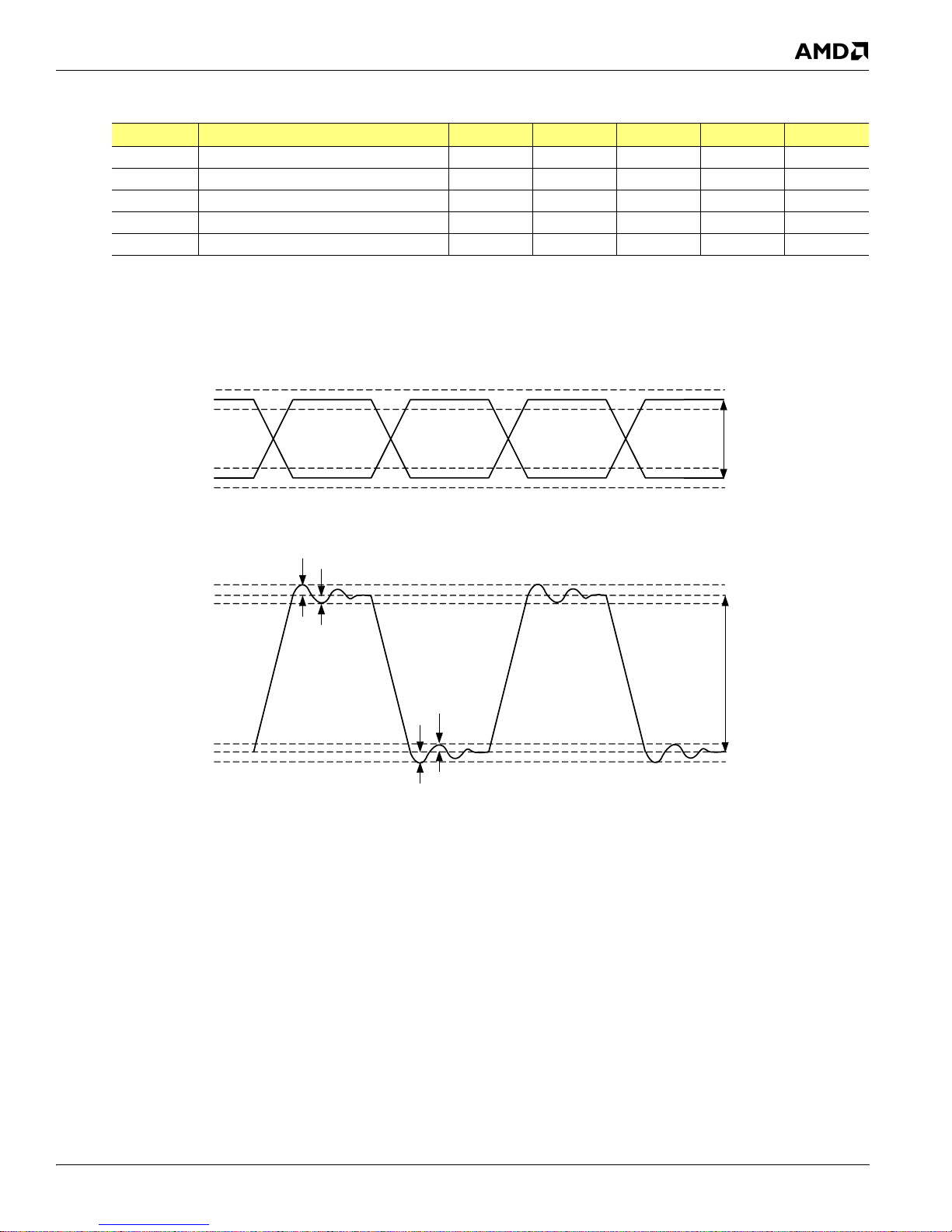
Electrical Characteristics
VSW
VHmax
VHmin
VLmax
VLmin
2VSW
VOS
VUS
Single-ended Waveforms
Differential Waveform
VOS
VUS
Table 5-11 DC Characteristics for the TMDS Interface Multiplexed on the PCI-E Gfx Lanes
Symbol Parameter Min Typical Max Unit Note
VH Single-ended High Level Output Voltage AVCC - 10 – AVCC + 10 mV 1
VL Single-ended Low Level Output Voltage AVCC - 600 – AVCC - 400 mV 1
VSW Single-ended Output Swing 400 – 600 mV
VOS Differential Output Overshoot (Ringing) – – 15%*2VSW –
VUS Differential Output Undershoot (Ringing) – – 25%*2VSW –
Notes:
1 AVCC stands for the termination supply voltage of the receiver, which is 3.3V +/- 5%.
2 Figure 5-1 below illustrates some of the DC Characteristics of the TMDS interface.
Figure 5-1 DC Characteristics of the TMDS Interfaces
© 2009 Advanced Micro Devices, Inc. 45732 AMD 780E Databook 3.10
Proprietary 5-5
Page 68

Electrical Characteristics
+257 to
+454mV
-257 to
-454mV
Differential Waveform
VCM = 1.125-
Single-ended Waveforms
Ground
Table 5-12 Electrical Requirements for the LVTM Interface in LVDS Mode
Symbol Parameter Min Typical Max Unit Note
VCM Differential Output Common-mode Voltage 1.125 – 1.375 V 1
DVCM
VH Single-ended High Level Output Voltage VCM + 0.125 – VCM + 0.225 V 1
VL Single-ended Low Level Output Voltage VCM - 0.225 – VCM - 0.125 V 1
VSW Single-ended Output Swing 257 – 454 mV 1
VOS Differential Output Overshoot (Ringing) – – 160 mV 1
VUS Differential Output Undershoot (Ringing) – – 160 mV 1
IDDLP Average Supply Current at LTPVDD18 – 10.0 – mA 2
IDDLV Average Supply Current at VDDLT18/33 – 100.0 – mA 2
IOL Output Low Current – 2.5 – mA
IOH Output High Current – 4.5 – mA
IPDLP Power Down Current at LTPVDD18 – 10.0 – A3
IPDLV Power Down Current at VDDLT18/33 – 10.0 – A3
Notes:
1 Differential termination is 100 ohms.
2 Measured under typical conditions, at minimum Differential Clock Frequency and maximum LVDS PLL VOC frequency.
3 Measured under typical conditions, based on typical leakage values.
4 Figure 5-2 below illustrates the DC Characteristics of the LVDS interface.
Differential Output Common-mode Voltage
Ripple
– – 150 mV 1
VSW
VSW
Figure 5-2 DC Characteristics of the LVDS Interface
1.375V
0V
45732 AMD 780E Databook 3.10 © 2009 Advanced Micro Devices, Inc.
5-6 Proprietary
Page 69

RS780E Thermal Characteristics
Table 5-13 Electrical Specifications for the DisplayPort™ Interface
Symbol Parameter Min Typ Max Unit Notes
UI
HIGH_RATE
UI
LOW_RATE
V
TX-DIFFp_p
V
TX-PREMMP-RATIO
Unit Interval for DP High Bit Rate (2.7
Gbps/lane)
Unit Interval for DP Reduced Bit Rate (1.62
Gbps/lane)
Differential Peak-to-Peak Output Voltage Level 0.34 - 0.92 V -
Pre-emphasis Level 0 - 7.2 dB -
5.2 RS780E Thermal Characteristics
This section describes some key thermal parameters of the RS780E. For a detailed discussion on these parameters
and other thermal design descriptions including package level thermal data and analysis, please consult the Thermal
Design and Analysis Guidelines
5.2.1 RS780E Thermal Limits
Table 5-14 RS780E Thermal Limits
Parameter Minimum Nominal Maximum Unit Note
Operating Case Temperature 0 — 95
Absolute Rated Junction
Temperature
Storage Temperature -40 — 60
Ambient Temperature 0 — 45
Thermal Design Power — 13 — W 4
Notes:
1 - The maximum operating case temperature is the die geometric top-center temperature measured via a thermocouple based on the
methodology given in the document Thermal Design and Analysis Guidelines for the RS780 Product Family, order# 44638 (Chapter 12).
This is the temperature at which the functionality of the chip is qualified.
2 - The maximum absolute rated junction temperature is the junction temperature at which the device can operate without causing
damage to the ASIC. This temperature can be measured via the integrated thermal diode described in the next section.
3 - The ambient temperature is defined as the temperature of the local intake air to the thermal management device. The maximum
ambient temperature is dependent on the heat sink's local ambient conditions as well as the chassis' external ambient, and the value
given here is based on AMD’s reference heat sink solution for the RS780E. Refer to Chapter 6 in the Thermal Design and Analysis
Guidelines for the RS780 Product Family, order# 44638, for heatsink and thermal design guidelines. Refer to Chapter 7 of the above
mentioned document for details of ambient conditions.
4 - Thermal Design Power (TDP) is defined as the highest power dissipated while running currently available worst case applications at
nominal voltages. Since the core power of modern ASICs using 65nm and smaller process technology can vary significantly, parts
specifically screened for higher core power were used for TDP measurement. The TDP is intended only as a design reference, and
the value given here is preliminary.
for the RS780 Product Family, order# 44638.
- 370 - ps High limit = +300 ppm
- 617 - ps High limit = +300 ppm
——115
Low limit = -5300 ppm
Low limit = -5300 ppm
°
C1
°
C2
°
C
°
C3
© 2009 Advanced Micro Devices, Inc. 45732 AMD 780E Databook 3.10
Proprietary 5-7
Page 70

5.2.2 Thermal Diode Characteristics
V
K T Nln
q
--------------------------------------------=
The RS780E has an on-die thermal diode, with its positive and negative terminals connected to the THERMALDIODE_P
and THERMALDIODE_N pins respectively. Combined with a thermal sensor circuit, the diode temperature, and hence
the ASIC temperature, can be derived from a differential voltage reading (
below:
where:
V = Difference of two base-to-emitter voltage readings, one using current = I and the other using current = N x I
N
= Ratio of the two thermal diode currents (=10 when using an ADI thermal sensor, e.g. ADM 1020, 1030)
= Ideality factor of the diode
K = Boltzman’s Constant
T = Temperature in Kelvin
q = Electron charge
RS780E Thermal Characteristics
V). The equation relating T to V is given
The series resistance of the thermal diode (RT) must be taken into account as it introduces an error in the reading
o
(for every 1.0, approximately 0.8
induced, plus any other known fixed error. Measured values of diode ideality factor and series resistance for the
R
T
diode circuit are defined in the Thermal Design and Analysis Guidelines
C is added to the reading). The sensor circuit should be calibrated to offset the
for the RS780 Product Family, order#
44638.
45732 AMD 780E Databook 3.10 © 2009 Advanced Micro Devices, Inc.
5-8 Proprietary
Page 71

Package Information
Mod-00085-Rev-03
5.3 Package Information
5.3.1 Physical Dimensions
Figure 5-1 and Table 5-15 describe the physical dimensions of the RS780E package. Figure 5-2 shows the detailed
ball arrangement for the RS780E.
Table 5-15 RS780E 528-Pin FCBGA Package Physical Dimensions
Ref. Min(mm) Typical (mm) Max. (mm)
c 0.48 0.58 0.68
A 1.69 1.84 1.99
A1 0.30 0.40 0.50
A2 0.81 0.86 0.91
b 0.40 0.50 0.60
D1 20.85 21.00 21.15
D2 - 8.58 -
D3 2.00 - -
D4 1.00 - -
E1 20.85 21.00 21.15
E2 - 7.70 -
E3 2.00 - -
E4 1.00 - -
F1 - 19.20 -
F2 - 19.20 -
e1 - 0.80 (min. pitch) -
ddd - - 0.20
Note: Maximum height of SMT components is 0.650 mm.
Figure 5-1 RS780E 528-Pin FCBGA Package Outline
© 2009 Advanced Micro Devices, Inc. 45732 AMD 780E Databook 3.10
Proprietary 5-9
Page 72

Package Information
Figure 5-2 RS780E Ball Arrangement (Bottom View)
5.3.2 Pressure Specification
To avoid damages to the ASIC (die or solder ball joint cracks) caused by improper mechanical assembly of the cooling
device, follow the recommendations below:
• It is recommended that the maximum load that is evenly applied across the contact area between the thermal
management device and the die does not exceed 6 lbf. Note that a total load of 4-6 lbf is adequate to secure the
thermal management device and achieve the lowest thermal contact resistance with a temperature drop across
the thermal interface material of no more than 3°C. Also, the surface flatness of the metal spreader should be
0.001 inch/1 inch.
• Pre-test the assembly fixture with a strain gauge to make sure that the flexing of the final assembled board and
the pressure applying around the ASIC package will not exceed 600 micron strain under any circumstances.
• Ensure that any distortion (bow or twist) of the board after SMT and cooling device assembly is within industry
45732 AMD 780E Databook 3.10 © 2009 Advanced Micro Devices, Inc.
5-10 Proprietary
Page 73

Package Information
1:1 ratio to pad, or
400µm max for the nine
corner balls’ openings
1:1 ratio to pad, or
400µm max for the eight
corner balls’ openings
1:1 ratio to pad, or
400µm max for the nine
corner balls’ openings
1:1 ratio to pad, or
400µm max for the nine
corner balls’ openings
1:1 ratio to pad,
with special
requirement for
corner balls
guidelines (IPC/EIA J-STD-001). For measurement method, refer to the industry approved technique described
in the manual IPC-TM-650, section 2.4.22.
5.3.3 Board Solder Reflow Process Recommendations
5.3.3.1 Stencil Opening Size for Solder Paste Pads on PCB
It is recommended that the stencil aperture for solder paste be kept at the same size as the land pads'. However, for
the nine (or eight) pads at each corner of the ASIC package, the size of the openings should not exceed 400µm (see
Figure 5-3 below). This recommendation is based on AMD’s sample land pattern design for the RS780E, which is
available from your AMD CSS representative.
5.3.3.2 Reflow Profile
A reference reflow profile is given below. Please note the following when using RoHS/lead-free solder (SAC105/305/405
Tin-Silver-Cu):
• The final reflow temperature profile will depend on the type of solder paste and chemistry of flux used in the SMT
process. Modifications to the reference reflow profile may be required in order to accommodate the requirements of
the other components in the application.
• An oven with 10 heating zones or above is recommended.
Figure 5-3 Recommended Stencil Opening Sizes for Solder Paste Pads on PCB
• To ensure that the reflow profile meets the target specification on both sides of the board, a different profile and oven
recipe for the first and second reflow may be required.
© 2009 Advanced Micro Devices, Inc. 45732 AMD 780E Databook 3.10
Proprietary 5-11
Page 74
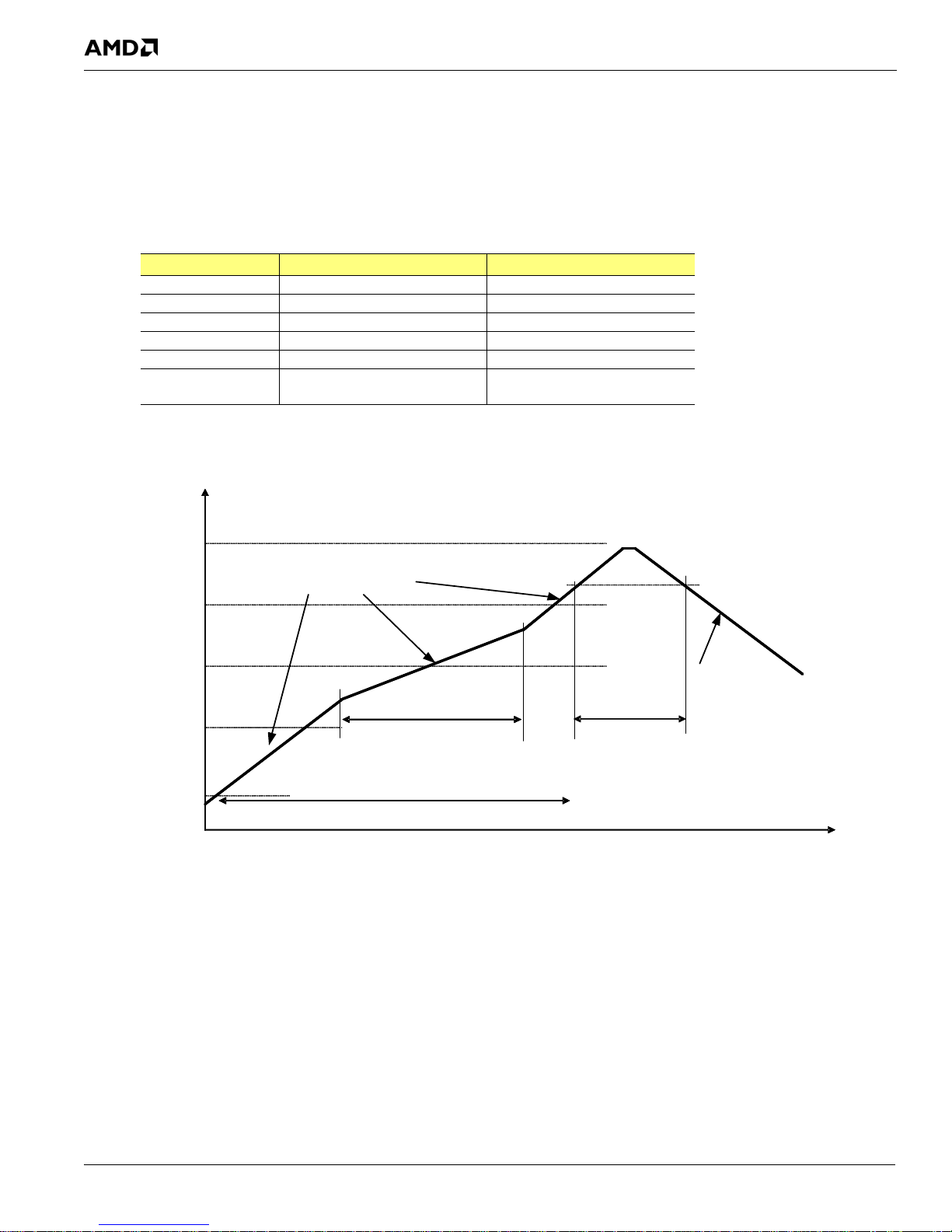
Package Information
50
250
150
200
100
Peak 245°C max.
220°C
Heating Time
Solder/Part Surface Temperature ( C)
170°C
50
250
150
200
100
C max.
220 C
o
120 - 240 sec max
Heating Time
°
C
60 – 120 sec max
130 C
60 – 80 sec typical
45 – 90 sec max
60 – 80 sec typical
Pre–heating Zone
Soldering Zone
Ramp Rate < 2 C / sec
°
Ramp Rate < 2 C / sec
Soaking Zone
°
• Mechanical stiffening can be used to minimize board warpage during reflow.
• It is suggested to decrease temperature cooling rate to minimize board warpage.
• This reflow profile applies only to RoHS/lead-free (high temperature) soldering process and it should not be used for
Eutectic solder packages. Damage may result if this condition is violated.
• Maximum 3 reflows are allowed on the same part.
Table 5-16 Recommended Board Solder Reflow Profile - RoHS/Lead-Free Solder
Profiling Stage Temperature Process Range
Overall Preheat Room temp to 220C 2 mins to 4 mins
Soaking Time 130C to 170C Typical 60 – 80 seconds
Liquidus 220C Typical 60 – 80 seconds
Ramp Rate Ramp up and Cooling <2C / second
Peak Max. 245C 235C +/-5C
Temperature at peak
within 5C
240C to 245C 10 – 30 seconds
Figure 5-4 RoHS/Lead-Free Solder (SAC305/405 Tin-Silver-Copper) Reflow Profile
45732 AMD 780E Databook 3.10 © 2009 Advanced Micro Devices, Inc.
5-12 Proprietary
Page 75
6.1 ACPI Power Management Implementation
This chapter describes the support for ACPI power management provided by the RS780E. The RS780E Northbridge
supports ACPI
required for meeting the power management specifications of PC2001, OnNow, and the Windows Logo Program and
Device Requirements version 2.1.
supported by the RS780E.
management scheme of the RS780E.
Table 6-1 ACPI States Supported by the RS780E
Graphics States:
D0 Full on, display active.
D1 Display Off. RS780E power on. Configuration registers, state, and main memory contents retained.
D3 Hot Similar to D1, with additional power saving and the graphics PLLs shut off.
D3 Cold RS780E power off.
Processor States:
S0/C0: Working State Working State. The processor is executing instructions.
S0/C1: Halt CPU Halt state. No instructions are executed. This state has the lowest latency on resume and contributes
S0/C2: Stop Grant
Caches Snoopable
S0/C3/C1e: Stop Grant
Caches Snoopable
System States:
S3: Standby
Suspend to RAM
S4: Hibernate
Suspend to Disk
S5: Soft Off System is off. OS re-boots when the system transitions to the working state.
G3: Mechanical Off Occurs when system power (AC or battery) is not present or is unable to keep the system in one of the
Revision 2.0. The hardware, system BIOS, video BIOS, and drivers of the RS780E have all the logic
Table 6-1, “ACPI States Supported by the RS780E,” describes the ACPI states
Table 6-2, “ACPI Signal Definitions,” describes the signals used in the ACPI power
ACPI State Description
minimum power savings.
Stop Grant or Cache Snoopable CPU state. This state offers more power savings but has a higher latency
on resume than the C1 state.
Processor is put into Stop Grant state. Caches are still snoopable. The HyperTransport link may be
disconnected and put into a low power state. System memory may be put into self-refresh.
System is off but context is saved to RAM. OEM support of this state is optional. System memory is put
into self-refresh.
System is off but context is saved to disk. When the system transitions to the working state, the OS is
resumed without a system re-boot.
other states.
Chapter 6
Power Management and ACPI
Note: Also supported are additional processor power states that are not part of the ACPI specification, e.g. C1E (C1
Enhanced) and C3 pop-up. Please refer to the
Programming Requirements,
Table 6-2 ACPI Signal Definitions
Signal Name Description Source
ALLOW_LDTSTOP Output to the Southbridge to allow LDTSTOP# assertion. Northbridge
LDTSTOP# HyperTransport™ Technology Stop: Enables and disables links during
system state transitions.
POWERON# Power On Power switch
RESET# Global Reset Southbridge
© 2009 Advanced Micro Devices, Inc. 45732 AMD 780E Databook 3.10
Proprietary 6-1
SB710 Databook, order# 45215, and the RS780 ASIC Family Register
order# 43291, for more information.
Southbridge
Page 76

6.2 Power Management for the Graphics Controller
The RS780E supports power management for the embedded graphics device as specified by the PCI Bus Power
Management Interface Specification version 1.0, according to which the integrated graphics core of the RS780E qualifies
as a device embedding a single function in the power management system.
6.2.1 PCI Function Power States
There are up to four power states defined for each PCI function associated with each PCI device in the system. These
power states are D0, D1, D2 and D3. D0 (on) consumes the most power while D3 (off) consumes the least. D1 and D2
enable levels of power savings in between those of D0 and D3. The concepts of these power states are universal for all
functions in the system. When transitioned to a given power management state, the intended functional behavior is
dependent upon the type (or class) of the function.
6.2.2 PCI Power Management Interface
The four basic power management operations are:
• Capabilities Reporting
• Power Status Reporting
• Setting Power State
• System Wakeup
All four of these capabilities are required for each power management function with the exception of wakeup event
generation.
Power Management for the Graphics Controller
This section describes the format of the registers in the PCI Configuration Space that are used by these power
management operations. The Status and Capabilities Pointer (CAP_PTR) fields have been highlighted to indicate where
the PCI Power Management features appear in the standard Configuration Space Header.
Table 6-3 Standard PCI Configuration Space Header Type 0
R e g i s t e r F i e l d s ( 3 2 B i t s )
MSB LSB
Device ID Vendor ID 00h (LSB)
Status (with Bit 4 set to 1) Command 04h
Class Code Revision ID 08h
BIST Header Type Latency Timer Cache Line Size 0Ch
Base Address Registers 10h
CardBus CIS Pointer 28h
Subsystem ID Subsystem Vendor ID 2Ch
Expansion ROM Base Address 30h
Reserved CAP_PTR 34h
Reserved 38h
Max_Lat Min_Gnt Interrupt Pin Interrupt Line 3Ch
Offset
14h
18h
1Ch
20h
24h
6.2.3 Capabilities List Data Structure in PCI Configuration Space
The Capabilities bit in the PCI Status register (offset = 06h) indicates whether or not the subject function implements a
linked list of extended capabilities. Specifically, if bit 4 is set, the CAP_PTR register is implemented to give offset to the
first item in the Capabilities link list.
45732 AMD 780E Databook 3.10 © 2009 Advanced Micro Devices, Inc.
6-2 Proprietary
Page 77
Power Management for the Graphics Controller
Table 6-4 PCI Status Register
Bits Default Value
15:05----Refer to PCI Local Bus Specification, Revision 2.2
04 1b Read Only This bit indicates whether this function implements a list of extended capabilities
03:00 0h Read Only Reserved
Read/
Write
Description
such as PCI power management. When set, this bit indicates the presence of
Capabilities. A value of 0 implies that this function does not implement
Capabilities.
The location of the Capabilities Pointer (CAP_PTR) depends on the PCI header type. See PCI Specification Revision 2.2
for specification of CAP_PTR offsets.
Table 6-5 Capabilities Pointer (CAP_PTR)
Bits Default Value
07:00 50h Read Only The CAP_PTR provides an offset in the PCI Configuration Space of the
Read/
Write
Description
function to access the location of the first item in the Capabilities linked list. The
CAP_PTR offset is DWORD aligned, so that the two least significant bits are
always zeros.
The graphics core implements extended capabilities of the AGP and Power Management. It needs to provide the
standardized register interface. The first entry in the chain of descriptors has to be the PMI descriptor, as this functionality
will be supported even if the RS780E operates as a PCI device. The Capabilities Identifier for Power Management is 01h.
6.2.4 Register Block Definition
This section describes the PCI Power Management Interface registers. These registers are implemented inside the Host
Interface (HI) as part of the configuration space of the device (RS780E).
Table 6-6 Power Management Register Block
Register Fields Offset
Capability Identifiers (CAP_ID) 00h
Next Item Pointer (NEXT_ITEM_PTR) 01h
Power Management Capabilities (PMC) 02h
Power Management Control/Status Register (PMCSR) 04h
Reserved 06h
The first 16 bits (Capabilities ID [offset = 0] and Next Item Pointer [offset = 1]) are used for the linked list infrastructure.
The next 32 bits (PMC [offset = 2] and PMCSR registers [offset = 4]) are required for compliance with this specification.
As with all PCI configuration registers, these registers may be accessed as bytes, 16-bit words, or 32-bit DWORDs. All of
the write operations to the reserved registers must be treated as no-ops. This implies that the access must be completed
normally on the bus and the data should be discarded. Read accesses to the reserved or the unimplemented registers must
be completed normally and a data value of 0000h should be returned.
© 2009 Advanced Micro Devices, Inc. 45732 AMD 780E Databook 3.10
Proprietary 6-3
Page 78

Power Management for the Graphics Controller
Table 6-7 Power Management Control/Status Register (PMCSR)
Field
Name
Power State 1:0 00 This field describes the power state of the graphics core.
Power State 15:2 0 These Read Only bits will return the clock status of each clock tree, generated inside the clock
Bits
Default
(Reset)
States Function
00 = D0 Normal operation, no power savings enabled
01 = D1 Sleeping state 1:
10 = D2 Sleeping state 2
11 = D3 Everything, except Host Interface, is turned off.
block.
The offset for each register is listed as an offset from the beginning of the linked list item that is determined either from
the CAP_PTR (if Power Management is the first item in the list) or the NEXT_ITEM_PTR of the previous item in the list.
6.2.5 Capability Identifier: CAP_ID (Offset = 0)
The Capability Identifier, when read by system software as 01h, indicates that the data structure currently being pointed to
is the PCI Power Management data structure. Each function of a PCI device may have only one item in its capability list
with CAP_ID set to 01h.
Description
Display is off
Host access to DRAM is allowed
Display is off.
All engines are off.
Graphics core does not respond to host accesses to the frame buffer.
Table 6-8 Capability Identifier (CAP_ID)
Bits Default Value
07:00 01h Read Only This field, when set to 01h, identifies the linked list item as being the PCI Power
Read/
Write
Description
Management registers
Figure 6-1, ‘Linked List for Capabilities,” shows the implementation of the capabilities list. The CAP_PTR gives the
location of the first item in the list. PCI Power Management registers have been stated as example in this list (although the
capabilities can be in any order).
• The first byte of each entry is required to be the ID of that capability. The PCI Power Management capability has an
ID of 01h.
• The next byte is a pointer giving an absolute offset in the functions PCI Configuration Space to the next item in the
list and must be DWORD aligned.
• If there are no more entries in the list, the NEXT_ITEM_PTR must be set to 0 to indicate an end of the linked list.
Each capability can then have registers following the NEXT_ITEM_PTR.
The definition of these registers (including layout, size, and bit definitions) is specific to each capability. The PCI Power
Management Register Block is defined in
Figure 6-1, ‘Linked List for Capabilities,” below.
45732 AMD 780E Databook 3.10 © 2009 Advanced Micro Devices, Inc.
6-4 Proprietary
Page 79
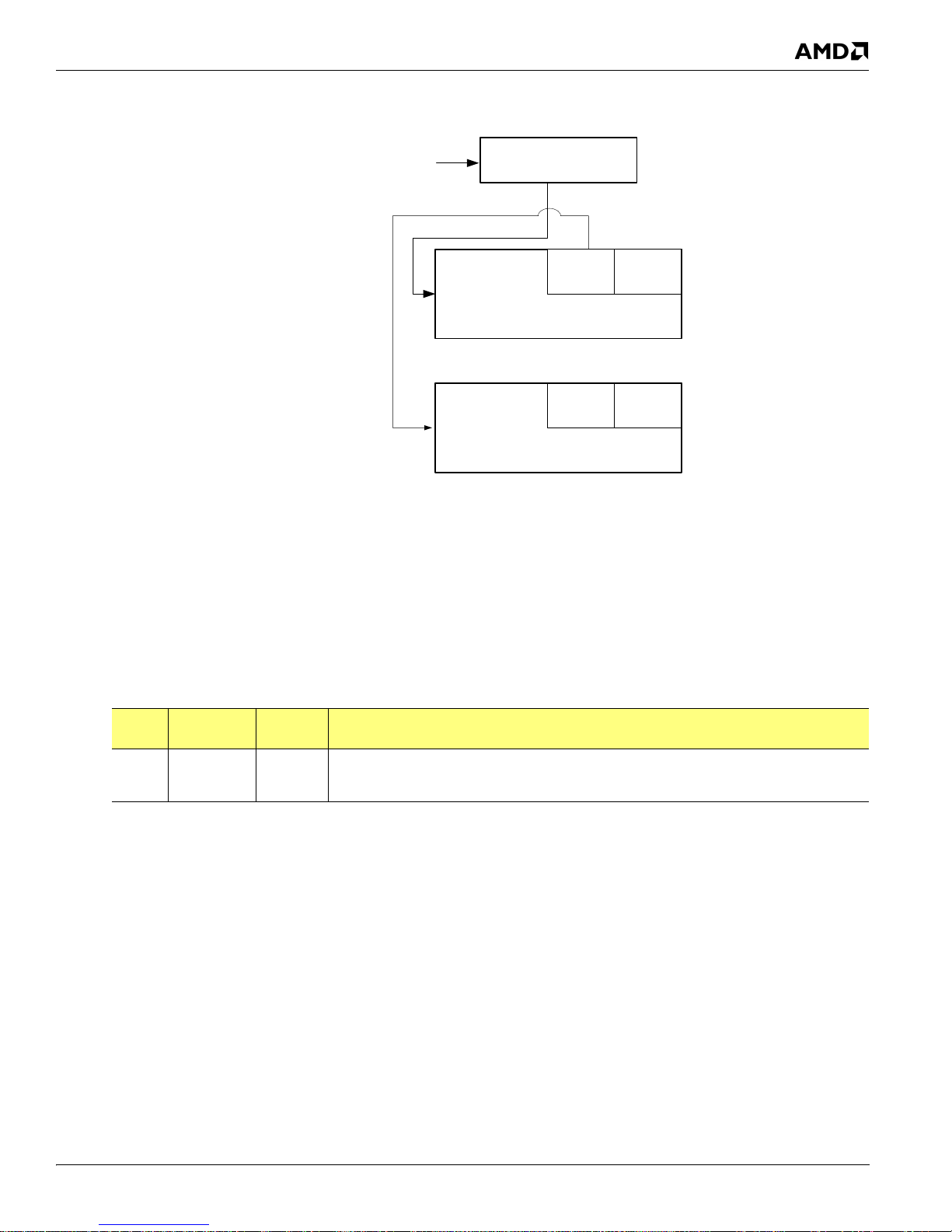
Power Management for the Graphics Controller
Cap_Ptr = 50h
8 bits
PCI Configuration Header
Offset 34h
025Ch
AGP Capability
0100h
PM Registers
Offset 5Ch
Offset 50h
Figure 6-1 Linked List for Capabilities
6.2.6 Next Item Pointer (Offset = 1)
The Next Item Pointer register describes the location of the next item in the capability list of the function. The value given
is an offset in the PCI Configuration Space of that function. This register must be set to 00h if the function does not
implement any other capabilities defined by the PCI Specifications for inclusion in the capabilities list, or if power
management is the last item in the list.
Table 6-9 Next Item Pointer (NEXT_ITEM_PTR)
Bits
07:00 80h Read Only This field provides an offset in the PCI Configuration Space of the function pointing to the location
Default
Value
Read/
Write
Description
of next item in the capability list of the function. For Power Management of the RS780E, this
pointer is set to 80h and it points to the next capability pointer of the MSI structure.
© 2009 Advanced Micro Devices, Inc. 45732 AMD 780E Databook 3.10
Proprietary 6-5
Page 80

6.2.7 PMC - Power Management Capabilities (Offset = 2)
The Power Management Capabilities register is a 16-bit Read Only register that provides information on the capabilities
of the function related to power management. The information in this register is generally static and is known at design
time.
Table 6-10 Power Management Capabilities – PMC
Power Management for the Graphics Controller
Bits Default Value
15:11 00111b Read Only This 5-bit field indicates the power states in which the function may assert PME#. A value of
10 001b Read Only RS780E supports D2.
09 001b Read Only RS780E supports D1.
08:06 000b Read Only Reserved
05 1b Read Only The Device Specific Initialization bit indicates whether special initialization of this function is
04 0b Read Only Reserved
03 0b Read Only Reserved
02:00 001b Read Only A value of 001b indicates that this function complies with Revision 1.0 of the PCI Power
Read/
Write
Description
0b for any bit indicates that the function is not capable of asserting the PME# signal while in
that power state.
bit(11) XXXX1b - PME# can be asserted from D0.
bit(12) XXX1Xb - PME# can be asserted from D1.
bit(13) XX1XXb - PME# can be asserted from D2.
bit(14) X0XXXb - PME# cannot be asserted from D3hot.
bit(15) 0XXXXb - PME# cannot be asserted from D3cold.
required (beyond the standard PCI configuration header) before the generic class device
driver is able to use it. The RS780E requires device specific initialization after Reset; this field
must therefore return a value 1 to the system.
Management Interface Specification.
45732 AMD 780E Databook 3.10 © 2009 Advanced Micro Devices, Inc.
6-6 Proprietary
Page 81
7.1 Test Capability Features
The RS780E has integrated test modes and capabilities. These test features cover both the ASIC and board level testing.
The ASIC tests provide a very high fault coverage and low DPM (Defect Per Million) ratio of the part. The board level
tests modes can be used for motherboard manufacturing and debug purposes. The following are the test modes of the
RS780E:
• Full scan implementation on the digital core logic that provides about 99% fault coverage through ATPG (Automatic
Test Pattern Generation Vectors).
• Dedicated test logic for the on-chip custom memory macros to provide complete coverage on these modules.
• Improved access to the analog modules and PLLs in the RS780E to allow full evaluation and characterization of these
modules.
• A JTAG test mode (which is not entirely compliant to the IEEE 1149.1 standard) to allow board level testing of
neighboring devices.
• An XOR TREE test mode on all the digital I/O’s to allow for proper soldering verification at the board level.
• A VOH/VOL test mode on all digital I/O’s to allow for proper verification of output high and output low voltages at
the board level.
These test modes can be accessed through the settings on the instruction register of the JTAG circuitry.
Chapter 7
Testability
7.2 Test Interface
Table 7-1 Pins on the Test Interface
Pin Name Ball number Type Description
TESTMODE D13 I IEEE 1149.1 test port reset
DDC_DATA0/AUX0N B8 I TMS: Test Mode Select (IEEE 1149.1 test mode select)
I2C_DATA A9 I TDI: Test Mode Data In (IEEE 1149.1 data in)
I2C_CLK B9 I TCLK: Test Mode Clock (IEEE 1149.1 clock)
TMDS_HPD D9 O TDO: Test Mode Data Out (IEEE 1149.1 data out)
POWERGOOD A10 I I/O Reset
7.3 XOR Test
7.3.1 Description of a Generic XOR Tree
An example of a generic XOR tree is shown in the Figure 7-1.
© 2009 Advanced Micro Devices, Inc. 45732 AMD 780E Databook 3.10
Proprietary 7-1
Page 82

XOR Test
XOR Start Signal
1
2
3
4
5
6
A
Figure 7-1 Example of a Generic XOR Tree
Pin A is assigned to the output direction, and pins 1 through 6 are assigned to the input direction. It can be seen that after
all pins 1 to 6 are assigned to logic 0 or 1, a logic change in any one of these pins will toggle the output pin A.
The following is the truth table for the XOR tree shown in
Table 7-2 Example of an XOR Tree
Test Vector
number
10000001
21000000
31100001
41110000
51111001
61111100
71111111
Input Pin 1 Input Pin 2 Input Pin 3 Input Pin 4 Input Pin 5 Input Pin 6 Output Pin A
7.3.2 Description of the RS780E XOR Tree
7.3.3 XOR Tree Activation
The RS780E chip enters the XOR tree test mode by means of the JTAG. First, the 8-bit instruction register of the JTAG is
loaded with the XOR instruction (“00001000”). This instruction assigns the input direction to all the pins except pin TDO,
which is assigned the output direction to serve as the output of the XOR tree. After loading, the JTAG is taken to the
Run-Test state for completion of the XOR tree initialization.
A
10MHz clock frequency for the Test Mode Clock (I2C_CLK) is recommended for the XOR TREE test mode. A pair of
differential clock at 10MHz should also be supplied to HT_REFCLKP/N to enable I/Os for testing.
Figure 7-1 The XOR start signal is assumed to be logic 1.
7.3.4 XOR Tree for the RS780E
The XOR start signal is applied at the TDI Pin of the JTAG circuitry and the output of the XOR tree is obtained at the
TDO Pin. Refer to
tree will cause the output to toggle.
There is no specific connection order to the signals on the tree. When the XOR tree is activated, any pin on the XOR tree
must be either pulled down or pulled up to the I/O voltage of the pin. Only pins that are
floating.
When differential signal pairs are listed as single entries on the XOR tree, opposite input values should be applied to the
two signals in each pair (e.g., for entry no. 1 on the tree, when “1” is applied to HT_RXCAD0P, “0” should be applied to
HT_RXCAD0N).
45732 AMD 780E Databook 3.10 © 2009 Advanced Micro Devices, Inc.
7-2 Proprietary
Table 7-3 for the list of the signals included on the XOR tree. A toggle of any of these balls in the XOR
not on the XOR tree can be left
Page 83

XOR Test
Table 7-3 RS780E XOR Tree
No. Pin Name
1 HT_RXCAD0P/N Y25/Y24
2 HT_RXCAD1P/N V22/V23
3 HT_RXCAD2P/N V25/V24
4 HT_RXCAD3P/N U24/U25
5 HT_RXCAD4P/N T25/T24
6 HT_RXCAD5P/N P22/P23
7 HT_RXCAD6P/N P25/P24
8 HT_RXCAD7P/N N24/N25
9 HT_RXCAD8P/N AC24/AC25
10 HT_RXCAD9P/N AB25/AB24
11 HT_RXCAD10P/N AA24/AA25
12 HT_RXCAD11P/N Y22/Y23
13 HT_RXCAD12P/N W21/W20
14 HT_RXCAD13P/N V21/V20
15 HT_RXCAD14P/N U20/U21
16 HT_RXCAD15P/N U19/U18
17 HT_RXCTL0P/N M22/M23
18 HT_RXCTL1P/N R21/R20
19 MEM_CKE AB18
20 MEM_CS# AB13
21 MEM_ODT V14
22 MEM_WE# AD18
23 MEM_RAS# W12
24 MEM_CAS# Y12
25 MEM_BA0 AD16
26 MEM_BA1 AE17
27 MEM_BA2 AD17
28 MEM_A0 AB12
29 MEM_A1 AE16
30 MEM_A2 V11
31 MEM_A3 AE15
32 MEM_A4 AA12
33 MEM_A5 AB16
34 MEM_A6 AB14
35 MEM_A7 AD14
Ball
Reference
No. Pin Name
36 MEM_A8 AD13
37 MEM_A9 AD15
38 MEM_A10 AC16
39 MEM_A11 AE13
40 MEM_A12 AC14
41 MEM_A13 Y14
42 MEM_DQ0 AA18
43 MEM_DQ1 AA20
44 MEM_DQ2 AA19
45 MEM_DQ3 Y19
46 MEM_DQ4 V17
47 MEM_DQ5 AA17
48 MEM_DQ6 AA15
49 MEM_DQ7 Y15
50 MEM_DQ8 AC20
51 MEM_DQ9 AD19
52 MEM_DQ10 AE22
53 MEM_DQ11 AC18
54 MEM_DQ12 AB20
55 MEM_DQ13 AD22
56 MEM_DQ14 AC22
57 MEM_DQ15 AD21
58 MEM_DM0 W17
59 MEM_DM1 AE19
60 MEM_DQS0P/N Y17/W18
61 MEM_DQS1P/N AD20/AE21
62 MEM_CKP/N V15/W14
63 GFX_RX0P/N D4/C4
64 GFX_RX1P/N A3/B3
65 GFX_RX2P/N C2/C1
66 GFX_RX3P/N E5/F5
67 GFX_RX4P/N G5/G6
68 GFX_RX5P/N H5/H6
69 GFX_RX6P/N J6/J5
70 GFX_RX7P/N J7/J8
Ball
Reference
© 2009 Advanced Micro Devices, Inc. 45732 AMD 780E Databook 3.10
Proprietary 7-3
Page 84

VOH/VOL Test
No. Pin Name
71 GFX_RX8P/N L5/L6
72 GFX_RX9P/N M8/L8
73 GFX_RX10P/N P7/M7
74 GFX_RX11P/N P5/M5
75 GFX_RX12P/N R8/P8
76 GFX_RX13P/N R6/R5
77 GFX_RX14P/N P4/P3
78 GFX_RX15P/N T4/T3
79 GPP_RX0P/N AE3/AD4
80 GPP_RX1P/N AE2/AD3
81 GPP_RX2P/N AD1/AD2
82 GPP_RX3P/N V5/W6
83 GPP_RX4P/N U5/U6
84 GPP_RX5P/N U8/U7
85 SB_RX0P/N AA8/Y8
Ball
Reference
86 SB_RX1P/N AA7/Y7
87 SB_RX2P/N AA5/AA6
88 SB_RX3P/N W5/Y5
89 LVDS_DIGON E9
90 LVDS_ENA_BL G12
91 LVDS_BLON F7
92 DAC_HSYNC A11
93 DAC_VSYNC B11
94 DAC_SCL F8
95 DDC_CLK0/AUX0P A8
96 HPD D10
97 DDC_DATA1/AUX1N A7
98 DDC_CLK1/AUX1P B7
7.4 VOH/VOL Test
7.4.1 Description of a Generic VOH/VOL Tree
The VOH/VOL logic gives signal output on I/O’s when test patterns are applied through the TEST_ODD and
TEST_EVEN inputs. Sample of a generic VOH/VOL tree is shown in
45732 AMD 780E Databook 3.10 © 2009 Advanced Micro Devices, Inc.
7-4 Proprietary
Figure 7-2.
Page 85

VOH/VOL Test
1
6
5
4
3
2
VOH/VOL
mode
TEST_ODD
TEST_EVEN
Figure 7-2 Sample of a Generic VOH/VOL Tree
7.4.2 VOH/VOL Tree Activation
The following is the truth table for the above VOH/VOL tree.
Table 7-4 Truth Table for the VOH/VOL Tree Outputs
Test Vector
Number
1 0 0 000000
2 0 1 010101
3 1 0 101010
4 1 1 111111
Refer to
To activate the VOH/VOL tree and run a VOH/VOL test, perform the sequence below:
1. Supply a 10MHz clock to the REF_CLKP pin and a 10MHz differential clock pair to the HT_REFCLKP/N pins to
enable I/Os for testing.
2. Set POWERGOOD to 0.
Section 7.4.3 for the list of pins that are on the VOH/VOL tree. VOH/VOL Tree Activation
TEST_ODD
Input
TEST_EVEN
Input
Output
Pin 1
Output
Pin 2
Output
Pin 3
Output
Pin 4
Output
Pin 5
Output
Pin 6
© 2009 Advanced Micro Devices, Inc. 45732 AMD 780E Databook 3.10
Proprietary 7-5
3. Set TESTMODE to 1.
4. Set DAC_SDA to 0.
5. Load JTAG instruction register with the instruction 0110 0011.
6. Load JTAG instruction register with the instruction 0010 0111.
7. Set POWERGOOD to 1.
Page 86

8. Load JTAG instruction register with the instruction 1001 1001.
9. Run test by loading JTAG data register with data 0000 0000 0000 00xy, where bit x is the input value for
TEST_ODD and bit y that for TEST_EVEN (see Table 7-4 above).
10. To end test, load JTAG instruction register with the instruction 0101 1101.
7.4.3 VOH/VOL Pin List
Table 7-5 shows the RS780E VOH/VOL tree. There is no specific order for connection. Under the Control column, an
“ODD” or “EVEN” indicates that the logical output of the pin is same as the “TEST_ODD” or “TEST_EVEN” input
respectively.
When a differential pair appear in the table as a single entry, the output of the positive (“P”) pin is indicated in the Control
column (see last paragraph for explanations), and the output of the negative pin (“N”) will be of the opposite value. For
example, for entry no. 1 on the tree, when TEST_EVEN is 1, HT_TXCAD0P will give a value of 1 and HT_TXCAD0N
will give a value of 0.
VOH/VOL Test
45732 AMD 780E Databook 3.10 © 2009 Advanced Micro Devices, Inc.
7-6 Proprietary
Page 87

VOH/VOL Test
Table 7-5 RS780E VOH/VOL Tree
No. Pin Name
1 HT_TXCAD0P/N D24/D25 Even
2 HT_TXCAD1P/N E24/E25 Odd
3 HT_TXCAD2P/N F24/F25 Even
4 HT_TXCAD3P/N F23/F22 Odd
5 HT_TXCAD4P/N H23/H22 Even
6 HT_TXCAD5P/N J25/J24 Odd
7 HT_TXCAD6P/N K24/K25 Even
8 HT_TXCAD7P/N K23/K22 Odd
9 HT_TXCAD8P/N F21/G21 Even
10 HT_TXCAD9P/N G20/H21 Odd
11 HT_TXCAD10P/N J20/J21 Even
12 HT_TXCAD11P/N J18/K17 Odd
13 HT_TXCAD12P/N L19/J19 Even
14 HT_TXCAD13P/N M19/L18 Odd
15 HT_TXCAD14P/N M21/P21 Even
16 HT_TXCAD15P/N P18/M18 Odd
17 HT_TXCTL0P/N M24/M25 Even
18 HT_TXCTL1P/N P19/R18 Odd
19 MEM_DQ0 AA18 Even
20 MEM_DQ1 AA20 Odd
21 MEM_DQ2 AA19 Even
22 MEM_DQ3 Y19 Odd
23 MEM_DQ4 V17 Even
24 MEM_DQ5 AA17 Odd
25 MEM_DQ6 AA15 Even
26 MEM_DQ7 Y15 Odd
27 MEM_DQ8 AC20 Even
28 MEM_DQ9 AD19 Odd
29 MEM_DQ10 AE22 Even
30 MEM_DQ11 AC18 Odd
31 MEM_DQ12 AB20 Even
32 MEM_DQ13 AD22 Odd
33 MEM_DQ14 AC22 Even
34 MEM_DQ15 AD21 Odd
35 MEM_DM0 W17 Even
Ball
Reference
Control
No. Pin Name
36 MEM_DM1 AE19 Odd
37 MEM_DQS0P/N Y17/W18 Even
38 MEM_DQS1P/N AD20/AE21 Odd
39 MEM_CKE AB18 Even
40 MEM_CS# AB13 Odd
41 MEM_ODT V14 Even
42 MEM_WE# AD18 Odd
43 MEM_RAS# W12 Even
44 MEM_CAS# Y12 Odd
45 MEM_BA0 AD16 Even
46 MEM_BA1 AE17 Odd
47 MEM_BA2 AD17 Even
48 MEM_A0 AB12 Odd
49 MEM_A1 AE16 Even
50 MEM_A2 V11 Odd
51 MEM_A3 AE15 Even
52 MEM_A4 AA12 Odd
53 MEM_A5 AB16 Even
54 MEM_A6 AB14 Odd
55 MEM_A7 AD14 Even
56 MEM_A8 AD13 Odd
57 MEM_A9 AD15 Even
58 MEM_A10 AC16 Odd
59 MEM_A11 AE13 Even
60 MEM_A12 AC14 Odd
61 MEM_A13 Y14 Even
62 MEM_CKP/N V15/W14 Odd
63 GFX_TX0P/N A5/B5 Even
64 GFX_TX1P/N A4/B4 Odd
65 GFX_TX2P/N C3/B2 Even
66 GFX_TX3P/N D1/D2 Odd
67 GFX_TX4P/N E2/E1 Even
68 GFX_TX5P/N F4/F3 Odd
69 GFX_TX6P/N F1/F2 Even
70 GFX_TX7P/N H4/H3 Odd
Ball
Reference
Control
© 2009 Advanced Micro Devices, Inc. 45732 AMD 780E Databook 3.10
Proprietary 7-7
Page 88

VOH/VOL Test
No. Pin Name
71 GFX_TX8P/N H1/H2 Even
72 GFX_TX9P/N J2/J1 Odd
73 GFX_TX10P/N K4/K3 Even
74 GFX_TX11P/N K1/K2 Odd
75 GFX_TX12P/N M4/M3 Even
76 GFX_TX13P/N M1/M2 Odd
77 GFX_TX14P/N N2/N1 Even
78 GFX_TX15P/N P1/P2 Odd
79 GPP_TX0P/N AC1/AC2 Even
80 GPP_TX1P/N AB4/AB3 Odd
81 GPP_TX2P/N AA2/AA1 Even
82 GPP_TX3P/N Y1/Y2 Odd
83 GPP_TX4P/N Y4/Y3 Even
84 GPP_TX5P/N V1/V2 Odd
85 SB_TX0P/N AD7/AE7 Even
Ball
Reference
Control
86 SB_TX1P/N AE6/AD6 Odd
87 SB_TX2P/N AB6/AC6 Even
88 SB_TX3P/N AD5/AE5 Odd
89 LVDS_BLON F7 Even
90 LVDS_ENA_BL G12 Odd
91 LVDS_DIGON E9 Even
92 DAC_VSYNC B11 Odd
93 DAC_HSYNC A11 Even
94 HPD D10 Odd
45732 AMD 780E Databook 3.10 © 2009 Advanced Micro Devices, Inc.
7-8 Proprietary
Page 89

Appendix A
Pin Listings
This appendix contains pin listings for the RS780E sorted in different ways. To go to the listing of interest, use the linked
cross-references below:
“RS780E Pin List Sorted by Ball Reference” on page A-2
“RS780E Pin List Sorted by Pin Name” on page A-7
© 2009 Advanced Micro Devices, Inc. 45732 AMD 780E Databook 3.10
Proprietary A-1
Page 90
A.1 RS780E Pin List Sorted by Ball Reference
Table A-1 RS780E Pin List Sorted by Ball Reference
Ball Ref Pin Name
A10 POWERGOOD
A11 DAC_HSYNC
A12 PLLVDD
A13 VDDLTP18
A14 VDDLT33
A15 VDDLT18
A16 TXCLK_LN
A17 TXOUT_U1P
A18 TXOUT_U0N
A19 TXOUT_L3P
A2 VSSAPCIE
A20 TXOUT_L2N
A21 TXOUT_L1P
A22 TXOUT_L0P
A23 VDDHTRX
A24 HT_RXCALN
A25 VSSAHT
A3 GFX_RX1P
A4 GFX_TX1P
A5 GFX_TX0P
A6 VDDPCIE
A7 DDC_DATA1/AUX1N
A8 DDC_CLK0/AUX0P
A9 I2C_DATA
AA1 GPP_TX2N
AA11 VDD_MEM
AA12 MEM_A4
AA14 VSS
AA15 MEM_DQ6
AA17 MEM_DQ5
AA18 MEM_DQ0
AA19 MEM_DQ2
AA2 GPP_TX2P
AA20 MEM_DQ1
AA21 VDDHTTX
AA22 HT_RXCLK1N
AA24 HT_RXCAD10P
AA25 HT_RXCAD10N
AA4 VSSAPCIE
AA5 SB_RX2P
AA6 SB_RX2N
AA7 SB_RX1P
Ball Ref Pin Name
AA8 SB_RX0P
AA9 VDDA18PCIE
AB1 VSSAPCIE
AB10 VDD_MEM
AB11 VSS
AB12 MEM_A0
AB13 MEM_CS#
AB14 MEM_A6
AB15 VSS
AB16 MEM_A5
AB17 VSS
AB18 MEM_CKE
AB19 VSS
AB2 VSSAPCIE
AB20 MEM_DQ12
AB21 VSS
AB22 VDDHTTX
AB23 HT_RXCLK1P
AB24 HT_RXCAD9N
AB25 HT_RXCAD9P
AB3 GPP_TX1N
AB4 GPP_TX1P
AB5 VSSAPCIE
AB6 SB_TX2P
AB7 VSSAPCIE
AB8 PCE_CALRN
AB9 VDDA18PCIE
AC1 GPP_TX0P
AC10 VDD_MEM
AC12 VSS
AC14 MEM_A12
AC16 MEM_A10
AC18 MEM_DQ11
AC2 GPP_TX0N
AC20 MEM_DQ8
AC22 MEM_DQ14
AC23 VDDHTTX
AC24 HT_RXCAD8P
AC25 HT_RXCAD8N
AC3 VSSAPCIE
AC4 VSSAPCIE
AC6 SB_TX2N
Pin Listings
Ball Ref Pin Name
AC8 PCE_CALRP
AD1 GPP_RX2P
AD10 VDD_MEM
AD11 VDD18_MEM
AD12 MEM_COMPN
AD13 MEM_A8
AD14 MEM_A7
AD15 MEM_A9
AD16 MEM_BA0
AD17 MEM_BA2
AD18 MEM_WE#
AD19 MEM_DQ9
AD2 GPP_RX2N
AD20 MEM_DQS1P
AD21 MEM_DQ15
AD22 MEM_DQ13
AD23 IOPLLVSS
AD24 VDDHTTX
AD25 VSSAHT
AD3 GPP_RX1N
AD4 GPP_RX0N
AD5 SB_TX3P
AD6 SB_TX1N
AD7 SB_TX0P
AD8 THERMALDIODE_N
AD9 VDDA18PCIE
AE1 VSSAPCIE
AE10 VDD_MEM
AE11 VDD18_MEM
AE12 MEM_COMPP
AE13 MEM_A11
AE14 VSS
AE15 MEM_A3
AE16 MEM_A1
AE17 MEM_BA1
AE18 MEM_VREF
AE19 MEM_DM1
AE2 GPP_RX1P
AE20 VSS
AE21 MEM_DQS1N
AE22 MEM_DQ10
AE23 IOPLLVDD18
45732 AMD 780E Databook 3.10 © 2009 Advanced Micro Devices, Inc.
A-2 Proprietary
Page 91
Pin Listings
Ball Ref Pin Name
AE24 IOPLLVDD
AE25 VDDHTTX
AE3 GPP_RX0P
AE4 VSSAPCIE
AE5 SB_TX3N
AE6 SB_TX1P
AE7 SB_TX0N
AE8 THERMALDIODE_P
AE9 VDDA18PCIE
B1 VSSAPCIE
B10 STRP_DATA
B11 DAC_VSYNC
B12 PLLVSS
B13 VSSLTP18
B14 VDDLT33
B15 VDDLT18
B16 TXCLK_LP
B17 TXOUT_U1N
B18 TXOUT_U0P
B19 TXOUT_L3N
B2 GFX_TX2N
B20 TXOUT_L2P
B21 TXOUT_L1N
B22 TXOUT_L0N
B23 VDDHTRX
B24 HT_TXCALP
B25 HT_TXCALN
B3 GFX_RX1N
B4 GFX_TX1N
B5 GFX_TX0N
B6 VDDPCIE
B7 DDC_CLK1/AUX1P
B8 DDC_DATA0/AUX0N
B9 I2C_CLK
C1 GFX_RX2N
C10 LDTSTOP#
C12 ALLOW_LDTSTOP
C14 VSSLT
C16 VSSLT
C18 VSSLT
C2 GFX_RX2P
C20 VSSLT
C22 VSSLT
C23 HT_RXCALP
Ball Ref Pin Name
C24 HT_REFCLKN
C25 HT_REFCLKP
C3 GFX_TX2P
C4 GFX_RX0N
C6 VDDPCIE
C8 AUX_CAL
D1 GFX_TX3P
D10 HPD
D11 VSS
D12 SUS_STAT#
D13 TESTMODE
D14 PLLVDD18
D15 VSSLT
D16 TXCLK_UP
D17 TXCLK_UN
D18 TXOUT_U3P
D19 TXOUT_U3N
D2 GFX_TX3N
D20 TXOUT_U2P
D21 TXOUT_U2N
D22 VDDHTRX
D23 VSSAHT
D24 HT_TXCAD0P
D25 HT_TXCAD0N
D3 VSSAPCIE
D4 GFX_RX0P
D5 VSSAPCIE
D6 VDDPCIE
D7 VDDA18PCIEPLL
D8 SYSRESET#
D9 TMDS_HPD
E1 GFX_TX4N
E11 REFCLK_P
E12 AVDD
E14 VSS
E15 VSS
E17 RESERVED
E18 GREEN
E19 BLUE
E2 GFX_TX4P
E20 VSSLT
E21 VDDHTRX
E22 VSSAHT
E24 HT_TXCAD1P
Ball Ref Pin Name
E25 HT_TXCAD1N
E4 VSSAPCIE
E5 GFX_RX3P
E6 VDDPCIE
E7 VDDA18PCIEPLL
E8 DAC_SDA
E9 LVDS_DIGON
F1 GFX_TX6P
F11 REFCLK_N
F12 AVDD
F14 AVDDDI
F15 RESERVED
F17 RESERVED
F18 GREEN#
F19 BLUE#
F2 GFX_TX6N
F20 VDDHTRX
F21 HT_TXCAD8P
F22 HT_TXCAD3N
F23 HT_TXCAD3P
F24 HT_TXCAD2P
F25 HT_TXCAD2N
F3 GFX_TX5N
F4 GFX_TX5P
F5 GFX_RX3N
F6 VDDPCIE
F7 LVDS_BLON
F8 DAC_SCL
F9 VDD18
G1 VSSAPCIE
G11 RESERVED
G12 LVDS_ENA_BL
G14 DAC_RSET
G15 AVSSDI
G17 RED#
G18 RED
G19 VDDHTRX
G2 VSSAPCIE
G20 HT_TXCAD9P
G21 HT_TXCAD8N
G22 VSSAHT
G24 VSSAHT
G25 VSSAHT
G4 VSSAPCIE
© 2009 Advanced Micro Devices, Inc. 45732 AMD 780E Databook 3.10
Proprietary A-3
Page 92

Pin Listings
Ball Ref Pin Name
G5 GFX_RX4P
G6 GFX_RX4N
G7 VDDPCIE
G8 VSS
G9 VDD18
H1 GFX_TX8P
H11 VDD33
H12 VDD33
H14 AVSSQ
H15 AVDDQ
H17 VDDA18HTPLL
H18 VDDHTRX
H19 VSSAHT
H2 GFX_TX8N
H20 VSSAHT
H21 HT_TXCAD9N
H22 HT_TXCAD4N
H23 HT_TXCAD4P
H24 HT_TXCLK0P
H25 HT_TXCLK0N
H3 GFX_TX7N
H4 GFX_TX7P
H5 GFX_RX5P
H6 GFX_RX5N
H7 VSSAPCIE
H8 VDDPCIE
H9 VDDA18PCIE
J1 GFX_TX9N
J10 VDDA18PCIE
J11 VDDC
J12 VSS
J14 VDDC
J15 VSS
J16 VDDC
J17 VDDHT
J18 HT_TXCAD11P
J19 HT_TXCAD12N
J2 GFX_TX9P
J20 HT_TXCAD10P
J21 HT_TXCAD10N
J22 VSSAHT
J24 HT_TXCAD5N
J25 HT_TXCAD5P
J4 VSSAPCIE
Ball Ref Pin Name
J5 GFX_RX6N
J6 GFX_RX6P
J7 GFX_RX7P
J8 GFX_RX7N
J9 VDDPCIE
K1 GFX_TX11P
K10 VDDA18PCIE
K11 VSS
K12 VDDC
K14 VSS
K15 VDDC
K16 VDDHT
K17 HT_TXCAD11N
K2 GFX_TX11N
K22 HT_TXCAD7N
K23 HT_TXCAD7P
K24 HT_TXCAD6P
K25 HT_TXCAD6N
K3 GFX_TX10N
K4 GFX_TX10P
K9 VDDPCIE
L1 VSSAPCIE
L10 VDDA18PCIE
L11 VDDC
L12 VSS
L14 VDDC
L15 VSS
L16 VDDHT
L17 VSSAHT
L18 HT_TXCAD13N
L19 HT_TXCAD12P
L2 VSSAPCIE
L20 HT_TXCLK1N
L21 HT_TXCLK1P
L22 VSSAHT
L24 VSSAHT
L25 VSSAHT
L4 VSSAPCIE
L5 GFX_RX8P
L6 GFX_RX8N
L7 VSSAPCIE
L8 GFX_RX9N
L9 VDDPCIE
M1 GFX_TX13P
Ball Ref Pin Name
M10 VDDA18PCIE
M11 VSS
M12 VDDC
M13 VDDC
M14 VSS
M15 VDDC
M16 VDDHT
M17 VDDHTTX
M18 HT_TXCAD15N
M19 HT_TXCAD13P
M2 GFX_TX13N
M20 VSSAHT
M21 HT_TXCAD14P
M22 HT_RXCTL0P
M23 HT_RXCTL0N
M24 HT_TXCTL0P
M25 HT_TXCTL0N
M3 GFX_TX12N
M4 GFX_TX12P
M5 GFX_RX11N
M6 VSSAPCIE
M7 GFX_RX10N
M8 GFX_RX9P
M9 VDDPCIE
N1 GFX_TX14N
N12 VDDC
N13 VSS
N14 VDDC
N2 GFX_TX14P
N22 VSSAHT
N24 HT_RXCAD7P
N25 HT_RXCAD7N
N4 VSSAPCIE
P1 GFX_TX15P
P10 VDDA18PCIE
P11 VDDC
P12 VSS
P13 VDDC
P14 VDDC
P15 VSS
P16 VDDHT
P17 VDDHTTX
P18 HT_TXCAD15P
P19 HT_TXCTL1P
45732 AMD 780E Databook 3.10 © 2009 Advanced Micro Devices, Inc.
A-4 Proprietary
Page 93

Pin Listings
Ball Ref Pin Name
P2 GFX_TX15N
P20 VSSAHT
P21 HT_TXCAD14N
P22 HT_RXCAD5P
P23 HT_RXCAD5N
P24 HT_RXCAD6N
P25 HT_RXCAD6P
P3 GFX_RX14N
P4 GFX_RX14P
P5 GFX_RX11P
P6 VSSAPCIE
P7 GFX_RX10P
P8 GFX_RX12N
P9 VDDPCIE
R1 VSSAPCIE
R10 VDDA18PCIE
R11 VSS
R12 VDDC
R14 VSS
R15 VDDC
R16 VDDHT
R17 VDDHTTX
R18 HT_TXCTL1N
R19 VSSAHT
R2 VSSAPCIE
R20 HT_RXCTL1N
R21 HT_RXCTL1P
R22 VSSAHT
R24 VSSAHT
R25 VSSAHT
R4 VSSAPCIE
R5 GFX_RX13N
R6 GFX_RX13P
R7 VSSAPCIE
R8 GFX_RX12P
R9 VDDPCIE
T1 GFX_REFCLKN
T10 VDDA18PCIE
T11 VDDC
T12 VSS
T14 VDDC
T15 VDDC
T16 VDDHT
T17 VDDHTTX
Ball Ref Pin Name
T2 GFX_REFCLKP
T22 HT_RXCLK0P
T23 HT_RXCLK0N
T24 HT_RXCAD4N
T25 HT_RXCAD4P
T3 GFX_RX15N
T4 GFX_RX15P
T9 VDDPCIE
U1 GPP_REFCLKP
U10 VDDA18PCIE
U11 VSS
U12 VDDC
U14 VSS
U15 VSS
U16 VDDC
U17 VDDHTTX
U18 HT_RXCAD15N
U19 HT_RXCAD15P
U2 GPP_REFCLKN
U20 HT_RXCAD14P
U21 HT_RXCAD14N
U22 VSSAHT
U24 HT_RXCAD3P
U25 HT_RXCAD3N
U4 VSSAPCIE
U5 GPP_RX4P
U6 GPP_RX4N
U7 GPP_RX5N
U8 GPP_RX5P
U9 VDDPCIE
V1 GPP_TX5P
V11 MEM_A2
V12 VSS
V14 MEM_ODT
V15 MEM_CKP
V17 MEM_DQ4
V18 VDDHTTX
V19 VSSAHT
V2 GPP_TX5N
V20 HT_RXCAD13N
V21 HT_RXCAD13P
V22 HT_RXCAD1P
V23 HT_RXCAD1N
V24 HT_RXCAD2N
Ball Ref Pin Name
V25 HT_RXCAD2P
V3 GPPSB_REFCLKN
V4 GPPSB_REFCLKP
V5 GPP_RX3P
V6 VSSAPCIE
V7 VSSAPCIE
V8 VSSAPCIE
V9 VDDPCIE
W1 VSSAPCIE
W11 VSS
W12 MEM_RAS#
W14 MEM_CKN
W15 VSS
W17 MEM_DM0
W18 MEM_DQS0N
W19 VDDHTTX
W2 VSSAPCIE
W20 HT_RXCAD12N
W21 HT_RXCAD12P
W22 VSSAHT
W24 VSSAHT
W25 VSSAHT
W4 VSSAPCIE
W5 SB_RX3P
W6 GPP_RX3N
W7 VSSAPCIE
W8 VSSAPCIE
W9 VDDA18PCIE
Y1 GPP_TX3P
Y11 VDD_MEM
Y12 MEM_CAS#
Y14 MEM_A13
Y15 MEM_DQ7
Y17 MEM_DQS0P
Y18 VSS
Y19 MEM_DQ3
Y2 GPP_TX3N
Y20 VDDHTTX
Y21 VSSAHT
Y22 HT_RXCAD11P
Y23 HT_RXCAD11N
Y24 HT_RXCAD0N
Y25 HT_RXCAD0P
Y3 GPP_TX4N
© 2009 Advanced Micro Devices, Inc. 45732 AMD 780E Databook 3.10
Proprietary A-5
Page 94
Ball Ref Pin Name
Y4 GPP_TX4P
Y5 SB_RX3N
Y6 VSSAPCIE
Y7 SB_RX1N
Y8 SB_RX0N
Y9 VDDA18PCIE
Pin Listings
45732 AMD 780E Databook 3.10 © 2009 Advanced Micro Devices, Inc.
A-6 Proprietary
Page 95
Pin Listings
A.2 RS780E Pin List Sorted by Pin Name
Table A-2 RS780E Pin List Sorted by Pin Name
Pin Name Ball Ref
ALLOW_LDTSTOP C12
AUX_CAL C8
AVD D E1 2
AVD D F1 2
AVDDDI F14
AVD DQ H 15
AVSSDI G15
AVSSQ H14
BLUE E19
BLUE# F19
DAC_HSYNC A11
DAC_RSET G14
DAC_SCL F8
DAC_SDA E8
DAC_VSYNC B11
DDC_CLK0/AUX0P A8
DDC_CLK1/AUX1P B7
DDC_DATA0/AUX0N B8
DDC_DATA1/AUX1N A7
GFX_REFCLKN T1
GFX_REFCLKP T2
GFX_RX0N C4
GFX_RX0P D4
GFX_RX10N M7
GFX_RX10P P7
GFX_RX11N M5
GFX_RX11P P5
GFX_RX12N P8
GFX_RX12P R8
GFX_RX13N R5
GFX_RX13P R6
GFX_RX14N P3
GFX_RX14P P4
GFX_RX15N T3
GFX_RX15P T4
GFX_RX1N B3
GFX_RX1P A3
GFX_RX2N C1
GFX_RX2P C2
GFX_RX3N F5
GFX_RX3P E5
Pin Name Ball Ref
GFX_RX4N G6
GFX_RX4P G5
GFX_RX5N H6
GFX_RX5P H5
GFX_RX6N J5
GFX_RX6P J6
GFX_RX7N J8
GFX_RX7P J7
GFX_RX8N L6
GFX_RX8P L5
GFX_RX9N L8
GFX_RX9P M8
GFX_TX0N B5
GFX_TX0P A5
GFX_TX10N K3
GFX_TX10P K4
GFX_TX11N K2
GFX_TX11P K1
GFX_TX12N M3
GFX_TX12P M4
GFX_TX13N M2
GFX_TX13P M1
GFX_TX14N N1
GFX_TX14P N2
GFX_TX15N P2
GFX_TX15P P1
GFX_TX1N B4
GFX_TX1P A4
GFX_TX2N B2
GFX_TX2P C3
GFX_TX3N D2
GFX_TX3P D1
GFX_TX4N E1
GFX_TX4P E2
GFX_TX5N F3
GFX_TX5P F4
GFX_TX6N F2
GFX_TX6P F1
GFX_TX7N H3
GFX_TX7P H4
GFX_TX8N H2
GFX_TX8P H1
Pin Name Ball Ref
GFX_TX9N J1
GFX_TX9P J2
GPP_REFCLKN U2
GPP_REFCLKP U1
GPP_RX0N AD4
GPP_RX0P AE3
GPP_RX1N AD3
GPP_RX1P AE2
GPP_RX2N AD2
GPP_RX2P AD1
GPP_RX3N W6
GPP_RX3P V5
GPP_RX4N U6
GPP_RX4P U5
GPP_RX5N U7
GPP_RX5P U8
GPP_TX0N AC2
GPP_TX0P AC1
GPP_TX1N AB3
GPP_TX1P AB4
GPP_TX2N AA1
GPP_TX2P AA2
GPP_TX3N Y2
GPP_TX3P Y1
GPP_TX4N Y3
GPP_TX4P Y4
GPP_TX5N V2
GPP_TX5P V1
GPPSB_REFCLKN V3
GPPSB_REFCLKP V4
GREEN E18
GREEN# F18
HPD D10
HT_REFCLKN C24
HT_REFCLKP C25
HT_RXCAD0N Y24
HT_RXCAD0P Y25
HT_RXCAD10N AA25
HT_RXCAD10P AA24
HT_RXCAD11N Y23
HT_RXCAD11P Y22
HT_RXCAD12N W20
© 2009 Advanced Micro Devices, Inc. 45732 AMD 780E Databook 3.10
Proprietary A-7
Page 96

Pin Listings
Pin Name Ball Ref
HT_RXCAD12P W21
HT_RXCAD13N V20
HT_RXCAD13P V21
HT_RXCAD14N U21
HT_RXCAD14P U20
HT_RXCAD15N U18
HT_RXCAD15P U19
HT_RXCAD1N V23
HT_RXCAD1P V22
HT_RXCAD2N V24
HT_RXCAD2P V25
HT_RXCAD3N U25
HT_RXCAD3P U24
HT_RXCAD4N T24
HT_RXCAD4P T25
HT_RXCAD5N P23
HT_RXCAD5P P22
HT_RXCAD6N P24
HT_RXCAD6P P25
HT_RXCAD7N N25
HT_RXCAD7P N24
HT_RXCAD8N AC25
HT_RXCAD8P AC24
HT_RXCAD9N AB24
HT_RXCAD9P AB25
HT_RXCALN A24
HT_RXCALP C23
HT_RXCLK0N T23
HT_RXCLK0P T22
HT_RXCLK1N AA22
HT_RXCLK1P AB23
HT_RXCTL0N M23
HT_RXCTL0P M22
HT_RXCTL1N R20
HT_RXCTL1P R21
HT_TXCAD0N D25
HT_TXCAD0P D24
HT_TXCAD10N J21
HT_TXCAD10P J20
HT_TXCAD11N K17
HT_TXCAD11P J18
HT_TXCAD12N J19
HT_TXCAD12P L19
HT_TXCAD13N L18
Pin Name Ball Ref
HT_TXCAD13P M19
HT_TXCAD14N P21
HT_TXCAD14P M21
HT_TXCAD15N M18
HT_TXCAD15P P18
HT_TXCAD1N E25
HT_TXCAD1P E24
HT_TXCAD2N F25
HT_TXCAD2P F24
HT_TXCAD3N F22
HT_TXCAD3P F23
HT_TXCAD4N H22
HT_TXCAD4P H23
HT_TXCAD5N J24
HT_TXCAD5P J25
HT_TXCAD6N K25
HT_TXCAD6P K24
HT_TXCAD7N K22
HT_TXCAD7P K23
HT_TXCAD8N G21
HT_TXCAD8P F21
HT_TXCAD9N H21
HT_TXCAD9P G20
HT_TXCALN B25
HT_TXCALP B24
HT_TXCLK0N H25
HT_TXCLK0P H24
HT_TXCLK1N L20
HT_TXCLK1P L21
HT_TXCTL0N M25
HT_TXCTL0P M24
HT_TXCTL1N R18
HT_TXCTL1P P19
I2C_CLK B9
I2C_DATA A9
IOPLLVDD AE24
IOPLLVDD18 AE23
IOPLLVSS AD23
LDTSTOP# C10
LVDS_BLON F7
LVDS_DIGON E9
LVDS_ENA_BL G12
MEM_A0 AB12
MEM_A1 AE16
Pin Name Ball Ref
MEM_A10 AC16
MEM_A11 AE13
MEM_A12 AC14
MEM_A13 Y14
MEM_A2 V11
MEM_A3 AE15
MEM_A4 AA12
MEM_A5 AB16
MEM_A6 AB14
MEM_A7 AD14
MEM_A8 AD13
MEM_A9 AD15
MEM_BA0 AD16
MEM_BA1 AE17
MEM_BA2 AD17
MEM_CAS# Y12
MEM_CKE AB18
MEM_CKN W14
MEM_CKP V15
MEM_COMPN AD12
MEM_COMPP AE12
MEM_CS# AB13
MEM_DM0 W17
MEM_DM1 AE19
MEM_DQ0 AA18
MEM_DQ1 AA20
MEM_DQ10 AE22
MEM_DQ11 AC18
MEM_DQ12 AB20
MEM_DQ13 AD22
MEM_DQ14 AC22
MEM_DQ15 AD21
MEM_DQ2 AA19
MEM_DQ3 Y19
MEM_DQ4 V17
MEM_DQ5 AA17
MEM_DQ6 AA15
MEM_DQ7 Y15
MEM_DQ8 AC20
MEM_DQ9 AD19
MEM_DQS0N W18
MEM_DQS0P Y17
MEM_DQS1N AE21
MEM_DQS1P AD20
45732 AMD 780E Databook 3.10 © 2009 Advanced Micro Devices, Inc.
A-8 Proprietary
Page 97

Pin Listings
Pin Name Ball Ref
MEM_ODT V14
MEM_RAS# W12
MEM_VREF AE18
MEM_WE# AD18
PCE_CALRN AB8
PCE_CALRP AC8
PLLVDD A12
PLLVDD18 D14
PLLVSS B12
POWERGOOD A10
RED G18
RED# G17
REFCLK_N F11
REFCLK_P E11
RESERVED E17
RESERVED F15
RESERVED F17
RESERVED G11
SB_RX0N Y8
SB_RX0P AA8
SB_RX1N Y7
SB_RX1P AA7
SB_RX2N AA6
SB_RX2P AA5
SB_RX3N Y5
SB_RX3P W5
SB_TX0N AE7
SB_TX0P AD7
SB_TX1N AD6
SB_TX1P AE6
SB_TX2N AC6
SB_TX2P AB6
SB_TX3N AE5
SB_TX3P AD5
STRP_DATA B10
SUS_STAT# D12
SYSRESET# D8
TESTMODE D13
THERMALDIODE_N AD8
THERMALDIODE_P AE8
TMDS_HPD D9
TXCLK_LN A16
TXCLK_LP B16
TXCLK_UN D17
Pin Name Ball Ref
TXCLK_UP D16
TXOUT_L0N B22
TXOUT_L0P A22
TXOUT_L1N B21
TXOUT_L1P A21
TXOUT_L2N A20
TXOUT_L2P B20
TXOUT_L3N B19
TXOUT_L3P A19
TXOUT_U0N A18
TXOUT_U0P B18
TXOUT_U1N B17
TXOUT_U1P A17
TXOUT_U2N D21
TXOUT_U2P D20
TXOUT_U3N D19
TXOUT_U3P D18
VDD_MEM AA11
VDD_MEM AB10
VDD_MEM AC10
VDD_MEM AD10
VDD_MEM AE10
VDD_MEM Y11
VDD18 F9
VDD18 G9
VDD18_MEM AD11
VDD18_MEM AE11
VDD33 H11
VDD33 H12
VDDA18HTPLL H17
VDDA18PCIE AA9
VDDA18PCIE AB9
VDDA18PCIE AD9
VDDA18PCIE AE9
VDDA18PCIE H9
VDDA18PCIE J10
VDDA18PCIE K10
VDDA18PCIE L10
VDDA18PCIE M10
VDDA18PCIE P10
VDDA18PCIE R10
VDDA18PCIE T10
VDDA18PCIE U10
VDDA18PCIE W9
Pin Name Ball Ref
VDDA18PCIE Y9
VDDA18PCIEPLL D7
VDDA18PCIEPLL E7
VDDC J11
VDDC J14
VDDC J16
VDDC K12
VDDC K15
VDDC L11
VDDC L14
VDDC M12
VDDC M13
VDDC M15
VDDC N12
VDDC N14
VDDC P11
VDDC P13
VDDC P14
VDDC R12
VDDC R15
VDDC T11
VDDC T14
VDDC T15
VDDC U12
VDDC U16
VDDHT J17
VDDHT K16
VDDHT L16
VDDHT M16
VDDHT P16
VDDHT R16
VDDHT T16
VDDHTRX A23
VDDHTRX B23
VDDHTRX D22
VDDHTRX E21
VDDHTRX F20
VDDHTRX G19
VDDHTRX H18
VDDHTTX AA21
VDDHTTX AB22
VDDHTTX AC23
VDDHTTX AD24
VDDHTTX AE25
© 2009 Advanced Micro Devices, Inc. 45732 AMD 780E Databook 3.10
Proprietary A-9
Page 98
Pin Listings
Pin Name Ball Ref
VDDHTTX M17
VDDHTTX P17
VDDHTTX R17
VDDHTTX T17
VDDHTTX U17
VDDHTTX V18
VDDHTTX W19
VDDHTTX Y20
VDDLT18 A15
VDDLT18 B15
VDDLT33 A14
VDDLT33 B14
VDDLTP18 A13
VDDPCIE A6
VDDPCIE B6
VDDPCIE C6
VDDPCIE D6
VDDPCIE E6
VDDPCIE F6
VDDPCIE G7
VDDPCIE H8
VDDPCIE J9
VDDPCIE K9
VDDPCIE L9
VDDPCIE M9
VDDPCIE P9
VDDPCIE R9
VDDPCIE T9
VDDPCIE U9
VDDPCIE V9
VSS AA14
VSS AB11
VSS AB15
VSS AB17
VSS AB19
VSS AB21
VSS AC12
VSS AE14
VSS AE20
VSS D11
VSS E14
VSS E15
VSS G8
VSS J12
Pin Name Ball Ref
VSS J15
VSS K11
VSS K14
VSS L12
VSS L15
VSS M11
VSS M14
VSS N13
VSS P12
VSS P15
VSS R11
VSS R14
VSS T12
VSS U11
VSS U14
VSS U15
VSS V12
VSS W11
VSS W15
VSS Y18
VSSAHT A25
VSSAHT AD25
VSSAHT D23
VSSAHT E22
VSSAHT G22
VSSAHT G24
VSSAHT G25
VSSAHT H19
VSSAHT H20
VSSAHT J22
VSSAHT L17
VSSAHT L22
VSSAHT L24
VSSAHT L25
VSSAHT M20
VSSAHT N22
VSSAHT P20
VSSAHT R19
VSSAHT R22
VSSAHT R24
VSSAHT R25
VSSAHT U22
VSSAHT V19
VSSAHT W22
Pin Name Ball Ref
VSSAHT W24
VSSAHT W25
VSSAHT Y21
VSSAPCIE A2
VSSAPCIE AA4
VSSAPCIE AB1
VSSAPCIE AB2
VSSAPCIE AB5
VSSAPCIE AB7
VSSAPCIE AC3
VSSAPCIE AC4
VSSAPCIE AE1
VSSAPCIE AE4
VSSAPCIE B1
VSSAPCIE D3
VSSAPCIE D5
VSSAPCIE E4
VSSAPCIE G1
VSSAPCIE G2
VSSAPCIE G4
VSSAPCIE H7
VSSAPCIE J4
VSSAPCIE L1
VSSAPCIE L2
VSSAPCIE L4
VSSAPCIE L7
VSSAPCIE M6
VSSAPCIE N4
VSSAPCIE P6
VSSAPCIE R1
VSSAPCIE R2
VSSAPCIE R4
VSSAPCIE R7
VSSAPCIE U4
VSSAPCIE V6
VSSAPCIE V7
VSSAPCIE V8
VSSAPCIE W1
VSSAPCIE W2
VSSAPCIE W4
VSSAPCIE W7
VSSAPCIE W8
VSSAPCIE Y6
VSSLT C14
45732 AMD 780E Databook 3.10 © 2009 Advanced Micro Devices, Inc.
A-10 Proprietary
Page 99

Pin Listings
Pin Name Ball Ref
VSSLT C16
VSSLT C18
VSSLT C20
VSSLT C22
VSSLT D15
VSSLT E20
VSSLTP18 B13
© 2009 Advanced Micro Devices, Inc. 45732 AMD 780E Databook 3.10
Proprietary A-11
Page 100

This page is left blank intentionally.
Pin Listings
45732 AMD 780E Databook 3.10 © 2009 Advanced Micro Devices, Inc.
A-12 Proprietary
 Loading...