

Page 1

MODEL: PS 4LA
MODEL: PBM4
www.altoproaudio.com
Version 2.0
Page 2

CONTENT
1
1. Function Introduction…………………………………………………………….2
2. Specification……………………………………………………………………….2
3. Block Diagram……………………………………………………………………..3
4. Schematic Diagram……………………………………………………………….4
5. Wiring Diagram………………………………………………………… …………9
6. PCB Layout……………………………………………………………... ………..10
7. Test Procedure…………………………………………………………………....17
8. Exploded Views & Mechanical Parts List…………………………………….25
9. BOM…………………………………………………………………………………29
Page 3

The PBM4 is professional monitor. It is packed with some key features. For example: there is four MIC/LINE
Microphone Input
Electronically balanced, discrete input
Frequency response
10Hz to 55kHz, +/- 3dB
Distortion(THD&N)
0.05% at +4dBu, 1kHz
Gain
30dB
SNR(Signal to Noise Ratio)
>94dB
Line input
Electronically balanced
Frequency response
10Hz to 55kHz, +/- 3dB
Frequency response
0.05% at +4dBu, 1kHz
Gain
10dB
Microphone Input
1.4kOhm
Channel Insert return
2.5kOhm
All other inputs
10kOhm or greater
Tape out
1kOhm
All other outputs
120Ohm
Hi shelving
+/-15dB@12kHz
Low shelving
+/-15dB@80Hz
DSP Section
A/D and D/A converters
24bit
DSP resolution
24bit
Type of effects
REV+DELAY, and REV+CHORUS
REVERBS, Stereo DELAY, Chorus
Presets
16
Controls
16-position PRESET selector
CLIP LED
MUTE SWITCH with LED indicator
Noise(Bus noise)
Fader 0 dB, channels muted: -85dBr (ref.:
Fader 0 dB, all input channels assigned and
UNITY gain: -81dBr(ref.: +4dBu)
M max out ONITOR
+22dBu unbalanced, 1/4"jacks
FX Sends max out
+22dBu
Output Power
150W RMS (Nominal power)
Frequency Response
25HZ-20KHZ
Output Impedance
8 ohm
Dimensions
216.5
×
143.5
×
152.5mm(L
×W×
H)(8.5"
×
5.6"×6")
Net Weight
9.5kg
Shipping Weight
11.34 kg
Volume
2.8CFT
1. Function Introduction
2. Specification
2
inputs which provided with ultra low noise microphone pre-amplifiers and phantom power at +15V, each of
them features a 2-band equalizer, one AUX send and level control. FX MAIN/MONITOR outputs,16-position
multi-effect and soon.
Input channels
Impedance
Equalization
Main Mix Section
Amplifier Section
Physical
Page 4

D
3. Block Diagram
3
8
C
B
A
VER050105
11of
SHUNG LIN
RevisionModel No:
OUTPUT
AUX SEND2
T
RSS
7654321
1
2
TRS
POWER AMPLIFIER
ALTO PBM4
BLOCK DIAGRAM
( 4 POINT )
DFX SEND
DFX(DSP)
MAIN LEVEL
16KHz
6.3KHz
2.5KHz
1KHz
400Hz
160Hz
7-STAGE EQ
63Hz
MAIN BUS
TAPE OUT
2-TRACK
TAPE IN
LEVEL
2TK IN
Drawn By:
TRS
Sheet
MONITOR OUT
PBM4-MX
PBM4-MX BLOCK AND LEVEL DIAGRAM
13-Jan-2005
PBM4MX BLOCK-final.Sch
A2
Titel
Size
File:
Date:
MONITOR LEVEL
MAIN BUS
DFX (DSP)
MAIN-BUSMAIN BUS
MAIN BUS
AUX/DFX RET
T
RSRN
TN
3c5e1a4d2b
FX RETURN
DSP BOARD
PRESETS
MUTE
DSP FOOTSWITCH
OFF
PHANTOM
ON
+15V
[-6dB]
DFX SEND
[0dB]
LEVEL
[-10dB]
HA
LOW HI
[10dB]
213
CH INPUT
LOW-Z
HI-Z
[-40/-20dB]
[-30/-10dB]
2-STAGE EQ
(CH1-4)
1 2 3 4 5 6 78
D
C
B
A
Page 5
100NF
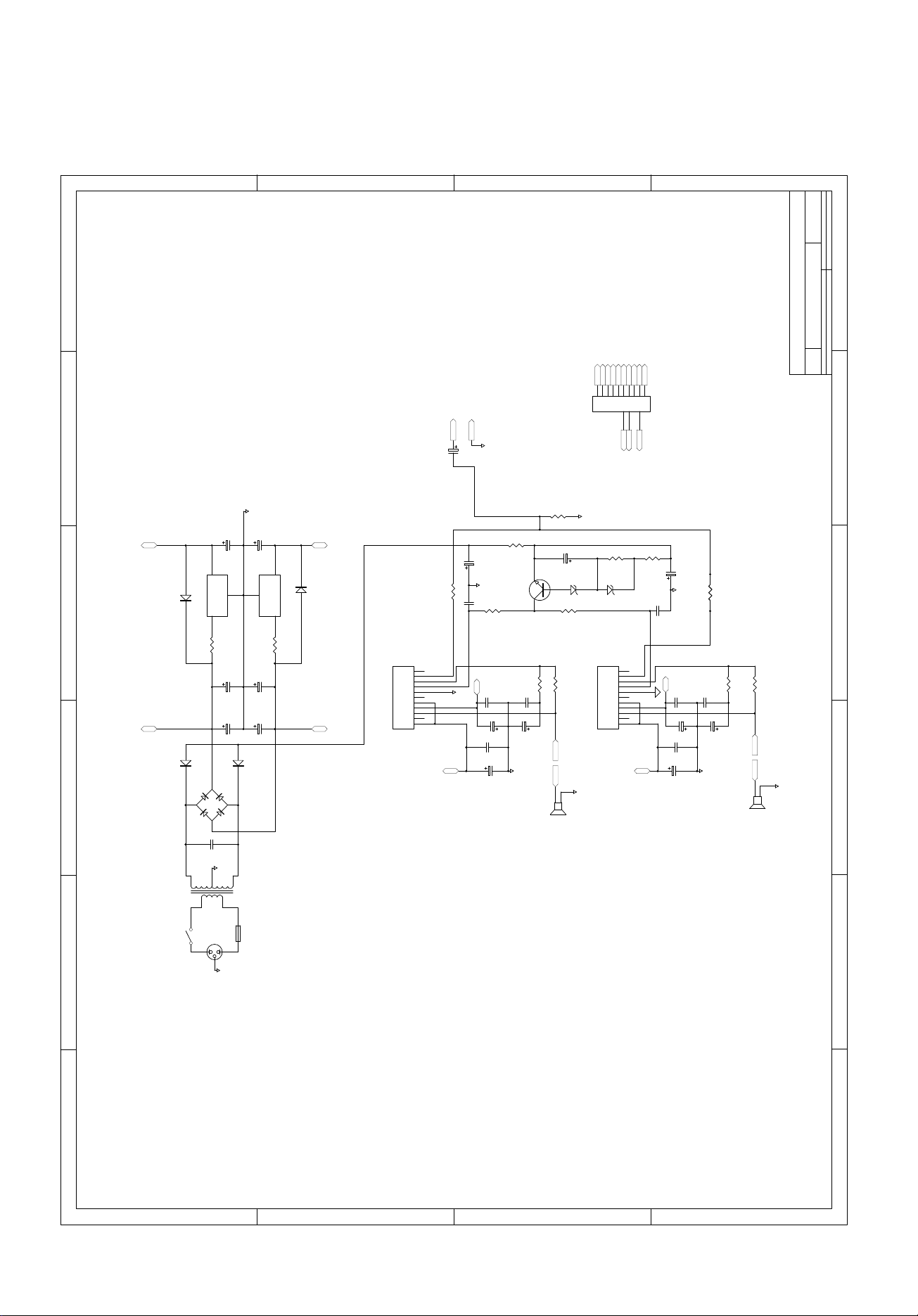
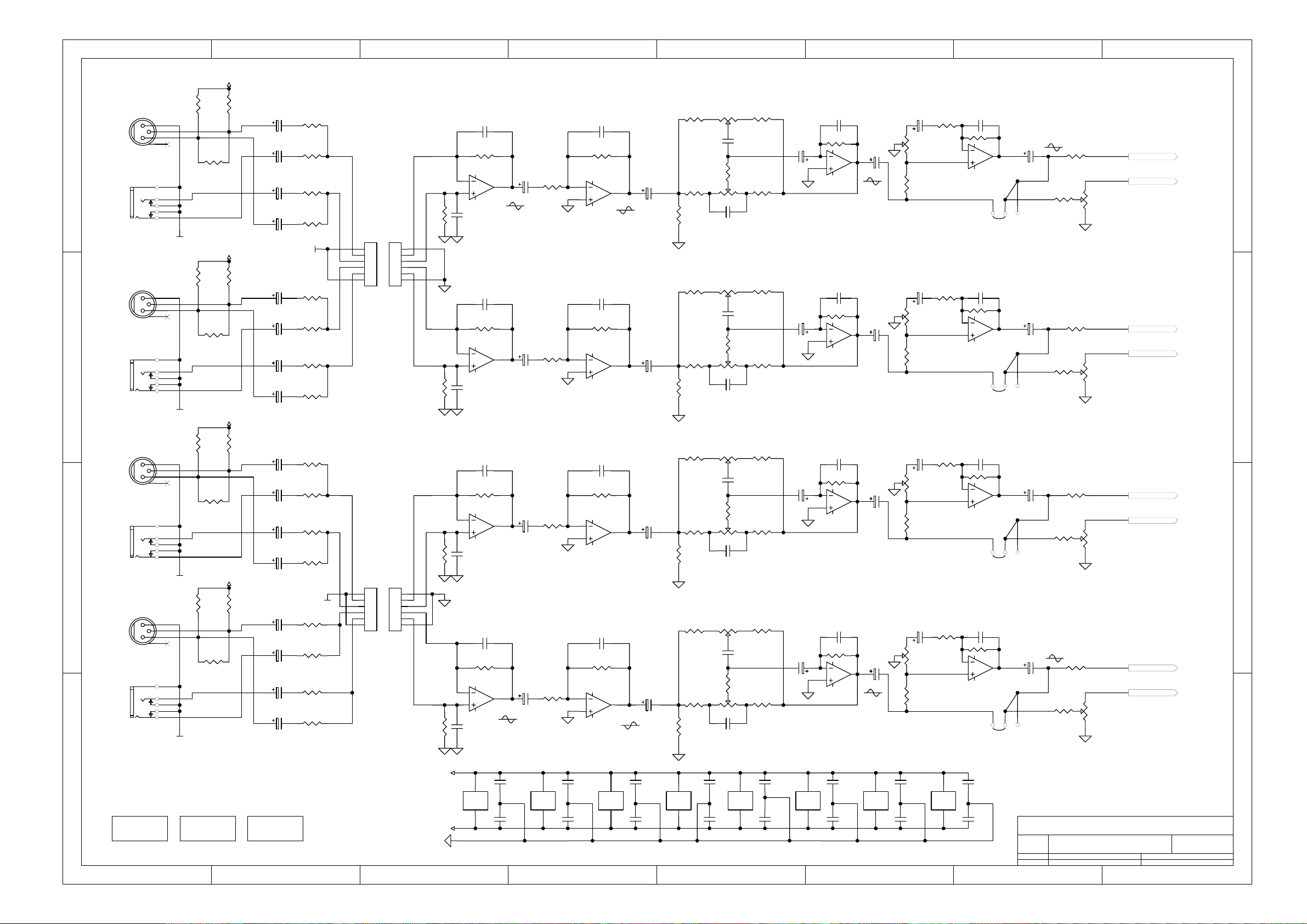
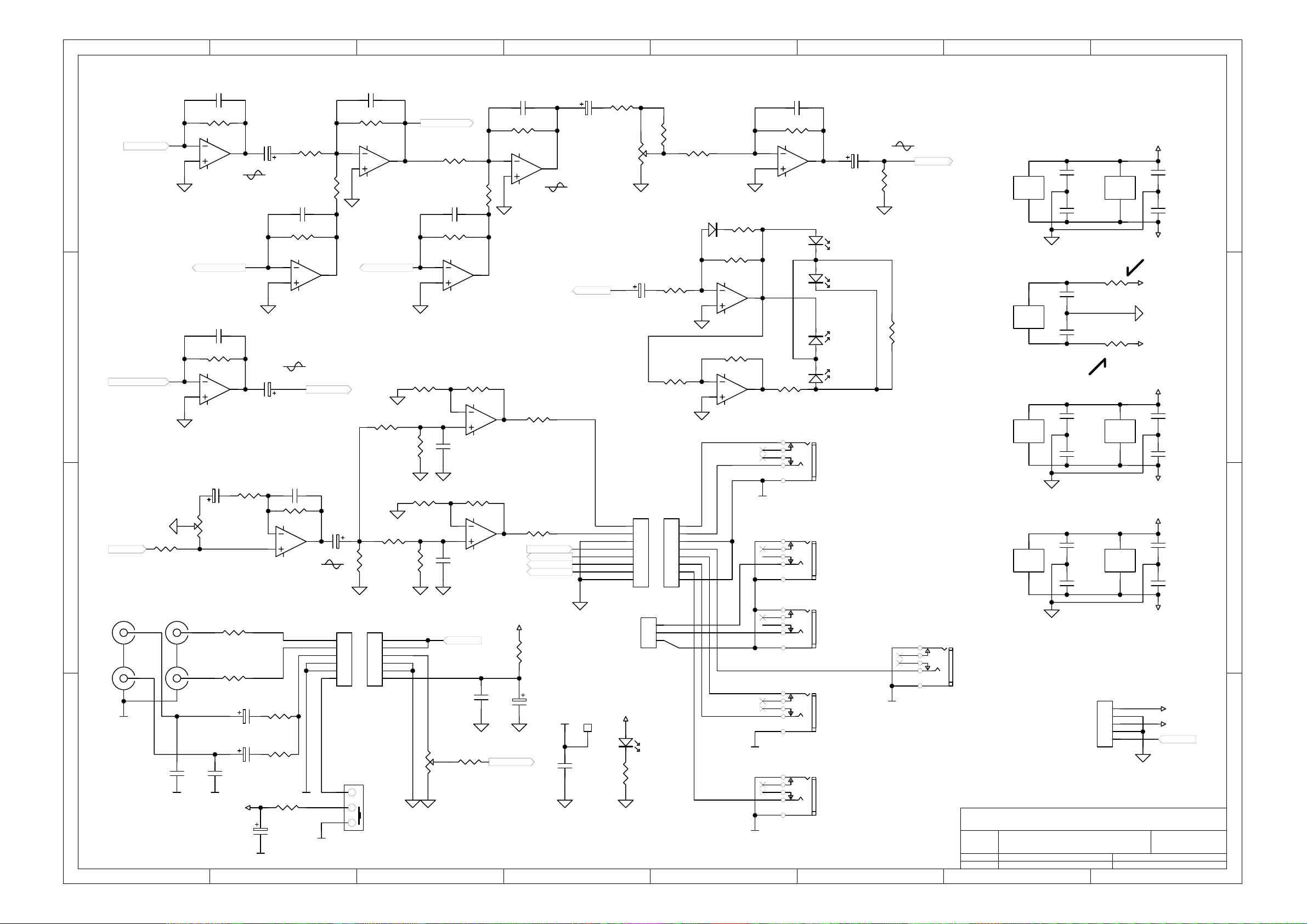
4. Schematic Diagram
4
2.2K
2.2K
R61KR2
47UF/25V
A
PING LU TANG
2004/11/01
PBM4
Number RevisionSize
C
Title
Date: 3-Feb-2005 Sheet of
File: PBM4 Drawn By:
33K
OUT2
SP2
GND
SP2
SPEAKER
D
654321
GND
C41
470UF/35V
C31
GND
C37
1000UF/35V
C35
6800UF/50V
D4
BU10--04
470UF/35V
3
OUT
GND
1
2
IN4004
3
C30
1000UF/35V
C13
6800UF/50V
D3
IN4004
IN
U3
7915
2
R9
200O
+15V
3
Vout
D6
IN4004
Vin
U6
7815
1
R3
95O
+VA
D5
IN4004
2
BR
1
4
C36
0.1UF/275V
C
INPUT-
INPUT+
GND
C20
1UF/50V
47UF/50V
GND
100NF
-VA
R15
C2
C6
C5
61.9K
100NF
C1
100NF
R8
100UF/50V
100UF/50V
-15V
C18
R5
2.2K
C15
2.6V
NC
11
+VIN
10
-VIN
9
MUTE
8
GND
7
NC
V+
V-
U1
LM3886
OUT
NC
-VA
V+
GND
6
5
4
3
2
1
+VA+VA
B
INPUT+
INPUT-
-15V
GND
+15V
GND
SP2
OUT2
SP1
OUT1
10
CN2
R13
47K
GND
100
GND
C19
34.9V
R4
100NF
47UF/25V
34.7V
1K
R1
OUT1
SP1
SP1
330UF/16V
D2
IN4737D1IN4737
R19
61.9K
33K
GND
SPEAKER
27V
U2
27V
LM3886
35V
Q1
2N5551
C10
C9
123456789
CON10
PC250
PC250
PC250
3.48K
R18
NC
+VIN
-VIN
MUTE
GND
NC
V+
VOUT
NC
V+
3.48K
35V
C14
20V
11
10
9
8
7
6
5
4
3
2
1
100UF/50V
GND
R7
C17
100NF
2.6V
R7
-VA
C4
100NF
C12
C3
100UF/50V
C11
C7
100NF
C8
100UF/50V
GND
R16
GND
T1
S1
SW SPST
D
AC
LAMP NEON
TRANS5
F?
FUSE1
GND
1 2 3 4 5 6
C
B
A
Page 6
7654321
5
+PHANTOM
R2
R1
6K8
CGND
CGND
6K8
R3
6K8
R7
10K
R10
10K
+PHANTOM
R5
6K8
+PHANTOM
C1
47U/50V
C7
47U/25V
C8
47U/25V
C2
47U/50V
C3
47U/50V
C10
47U/25V
C11
47U/25V
C4
47U/50V
R56
2K2
R57
22K
R58
22K
R59
2K2
CGND
R60
2K2
R61
22K
R62
22K
R63
2K2
1
2
3
4
5
6
CN1
CN2.0-6P-180
CN2
CN2.0-6P
1
2
3
4
5
6
R34
10K
R38
10K
C22
22P
R8
10K
U1A
4580M
2
3
C21
22P
1
C9
47U/25V
R74
1K
C25
22P
R11
10K
U3A
4580M
2
3
C24
22P
1
C12
47U/25V
R75
1K
C23
22P
EQ HI
10KHZ
R80
3K
6
5
U1B
4580M
C27
22P
7
C142
47U/25V
100Hz
EQ HI
10KHZ
R81
3K
6
5
U3B
4580M
7
C143
47U/25V
J1
JY5042-030G
D
CH1 INPUT
1
3
2
4
CH1 LINE
J2
SCJ-0658-1-Y
JY5042-030G
5e
1a
2b
4d
3c
J3
1
3
2
4
CH2 INPUT
CH2 LINE
C
J4
SCJ-0658-1-Y
5e
1a
2b
4d
3c
LOW
LOW
100Hz
R85
8K2
R177
2K2
R88
8K2
R178
2K2
R97
3K9
R99
3K9
R86
8K2
R89
8K2
VR1
B50K
VR5
B50K
C39
4N7(M)
VR2
B50K
C43
4N7(M)
C40
4N7(M)
VR6
B50K
C44
4N7(M)
R98
3K9
R87
8K2
R101
3K9
R90
8K2
C47
47U/25V
C51
47U/25V
LEVEL
C49
47U/25V
VR4
W50K
R35
22K
R112
8K2
C67
22P
R116
C50
U2A
4580M
36K
1
47U/25V
2
3
C66
22P
R105
1M
C48
U2B
4580M
47U/25V
7
6
5
J11
(PRE) POST
LEVEL
C53
47U/25V
VR8
W50K
R39
22K
R113
8K2
C70
22P
R117
C55
U4A
4580M
36K
1
47U/25V
2
3
C68
22P
R106
1M
C52
U4B
4580M
47U/25V
7
6
5
J12
(PRE) POST
PBM4 (1/4)
R9
R121
5K1
R122
5K1
10K
R12
10K
AUX-POST
VR3
W50K
AUX-POST
VR7
W50K
MAIN-BUS
FX SEND
MAIN-BUS
FX SEND
8
D
C
R6
R4
6K8
CGND
CGND
6K8
R42
6K8
R13
10K
R166
10K
+PHANTOM
R165
6K8
C5
47U/50V
C13
47U/25V
C14
47U/25V
C6
47U/50V
C138
47U/50V
C140
47U/25V
C141
47U/25V
C139
47U/50V
R64
2K2
R67
22K
R68
22K
R69
2K2
R170
2K2
R171
22K
R172
22K
R173
2K2
CGND
1
2
3
4
5
6
CN3
CN2.0-6P-180
CN4
CN2.0-6P
1
2
3
4
5
6
R43
10K
R126
10K
C26
22P
R14
10K
U5A
4580M
2
3
C29
22P
1
C15
47U/25V
R76
1K
C30
22P
R44
10K
U7A
4580M
2
3
C32
22P
1
C16
47U/25V
R77
1K
C28
22P
EQ HI
10KHZ
R82
3K
6
5
U5B
4580M
C31
22P
7
C144
47U/25V
100Hz
EQ HI
10KHZ
R83
3K
6
5
U7B
4580M
7
C145
47U/25V
100Hz
J5
JY5042-030G
1
3
2
4
CH3 INPUT
CH3 LINE
J6
SCJ-0658-1-Y
B
JY5042-030G
J17
5e
1a
2b
4d
3c
1
3
2
4
CH4 INPUT
CH4 LINE
J18
SCJ-0658-1-Y
5e
1a
2b
4d
3c
LOW
LOW
R91
8K2
R179
2K2
R94
8K2
R180
2K2
R100
3K9
R103
3K9
R92
8K2
R95
8K2
VR9
B50K
VR13
B50K
C41
4N7(M)
VR10
B50K
C45
4N7(M)
C42
4N7(M)
VR14
B50K
C46
4N7(M)
R102
3K9
R93
8K2
R104
3K9
R96
8K2
C56
47U/25V
C57
47U/25V
LEVEL
LEVEL
C54
47U/25V
VR12
W50K
R45
22K
C60
47U/25V
VR16
W50K
R48
22K
R114
8K2
R115
8K2
2
3
2
3
C71
22P
R118
36K
1
U6A
4580M
J13
(PRE) POST
C73
22P
R119
36K
1
U8A
4580M
J14
C61
47U/25V
C62
47U/25V
R123
5K1
R124
5K1
R15
10K
R16
10K
AUX-POST
VR11
W50K
AUX-POST
VR15
W50K
MAIN-BUS
FX SEND
B
MAIN-BUS
FX SEND
C69
22P
R107
1M
C58
U6B
4580M
C72
22P
R108
1M
U8B
4580M
47U/25V
7
C59
47U/25V
7
6
5
6
5
(PRE) POST
A
7 BAND EQ
PBM4-MX_4.SCH
1 2 3 4 5 6 78
MAIN SECTION
PBM4-MX_2.SCH
DSP SECTION
PBM4-MX_3.SCH
+VCC
-VCC
U1C
4580M
C81
84
100N
U2C
4580M
C82
100N
C83
84
100N
U3C
4580M
C84
100N
C85
84
100N
C86
100N
84
U4C
4580M
C87
100N
C88
100N
84
U5C
4580M
C89
100N
C90
100N
84
U6C
4580M
C91
100N
C92
100N
84
U7C
4580M
C93
100N
C94
100N
84
U8C
4580M
C95
100N
C96
100N
Titel
Size
Date:
File:
A3
PBM4 INPUT SECTION
PBM4
8-Jan-2005
PBM4-MX_1.Sch
Sheet
Drawn By:
RevisionModel No:
SHUNG LIN
A
V1.0
41of
Page 7
7654321
6
8
7 BAND EQ
C33 22P
R129
1K5
D
MAIN-BUS
2
3
U9A
4580M
1
C17
47U/25V
R71
5K6
R17
6K8
C118
10P
R130
39K
U19B
6
5
4580M
C35 22P
R135
C64
47U/25V
12K
U10A
4580M
1
R148
7K5
C19
EFFECT_IN
47U/25V
C36
22P
C
FX SEND
2
3
MONITOR OUT
VR21
R147
MAIN-OUT
B
J7
RCA4-SCP687
TAPE IN
27K
TAPE OUT
1 4
W50K
R65
2K2
2 5
R66
2K2
3
CGND
A
1 2 3 4 5 6 78
6
CGND
C76
100P
C77
100P
CGND
+PHANTOM
C74
47U/25V
C75
47U/25V
CGND
6
5
R46
22K
R47
22K
470R 1/2W
C146
470uF/50V
R181
U12B
4580M
CGND
7
CN2.0-6P-180
CGND
2
3
7
R120
36K
C65
47U/25V
1
2
3
4
5
6
CN10
SW1
3
2
1
6P-SL2020
C78
22P
R19
22K
U19A
4580M
MON_EQ_OOL_1MON_EQ_OOL_2
R53
22K
R54
22K
R52
22K
CN11
CN2.0-6P
1
2
3
4
5
6
MON_EQ_SOURCE
1
R137
5K6
R128
47K
R138
5K6
R127
47K
C134
10P
6
5
VR17
W50K
R70
22K
R136
39K
U20B
4580M
R21 10K
2
3
C119
56P
R22
10K
6
5
C120
56P
MAIN-OUT
R167
10K
R18
6K8
2
3
7
U13A
4580M
U13B
4580M
C125
100N
MAIN-BUS
C79
R125
5K6
U20A
4580M
100R 1/4W
1
100R 1/4W
7
+VCC
R32
100R 1/4W
22P
1
R149
R150
EFFECT_IN
RTN_L
RTN_R
FOOTSW
C135
100uF/25V
GND1
C18
R20
680R
47U/25V
VR20
B50K
MAIN LEVEL
C20
MAIN-OUT
47U/25V
CN5
CN2.0-8P-180
1
2
3
4
5
6
7
8
1
2
3
CN12
TO AMPLIFIER BOARD
TP1
C122
4U7/63V(NP)
CN2.5-3P-180
OPERATING
+VCC
D9
GR
R151
3K9/0805
R174
8K2
R51
100K
R78
1K
1
2
3
4
5
6
7
8
CN6
CN2.0-8P
R49
2K7
D1
RLS4148
2
3
6
5
R139
100K
R109
1M
4580M
R79
1K
U11A
U11B
4580M
CGND
CGND
CGND
2
3
U12A
4580M
30dB
10dB
1
0dB
10dB
R141
7
680R
J8
3c
4d
2b
1a
5e
SCJ-0658-1-Y
MONITOR OUT
SCJ-0658-1-Y
3c
4d
2b
1a
5e
J10
SCJ-0658-1-Y
3c
4d
2b
1a
5e
J16
3c
4d
2b
1a
5e
SCJ-0658-1-Y
FX RETURN
J19
3c
4d
2b
1a
5e
SCJ-0658-1-Y
FOOTSW
C34
22P
J9
R131
22K
C63
1
47U/25V
MAIN-OUT
R50
22K
D5
MAIN VMETER
3mm
GR
D6
3mm
GR
D7
3mm
YEL
D8
3mm
RED
R146
180R
OUT-1
MAIN POWER OUTPUT
(MIN. LOAD 8OHMS)
OUT-2
3c
4d
2b
1a
5e
SCJ-0658-1-Y
FX SEND
CGND
J15
Titel
Size
A3
Date:
File:
PBM4 (2/4)
84
U19C
C80
100N
4580M
C115
100N
84
C97
100N
U11C
4580M
84
U9C
C98
100N
C99
100N
4580M
C100
100N
84
U12C
C103
100N
4580M
C104
100N
PBM4 MAIN & OUTPUT SECTION
PBM4
8-Jan-2005
PBM4-MX_2.Sch
84
U20C
4580M
R133
22R 1/4W
R134
22R 1/4W
84
U10C
4580M
84
U13C
4580M
CN9
2.5-5P
1
2
3
4
5
Sheet
Drawn By:
+VCC
-VCC
+VCC
C116
100N
C117
100N
-VCC
+VCC
C101
100N
C102
100N
-VCC
+VCC
C105
100N
C106
100N
-VCC
+VCC
-VCC
MAIN-OUT
RevisionModel No:
SHUNG LIN
D
C
B
A
01
42of
Page 8

7654321
7
PBM4 (3/4)
8
R25
10K
U10B
6
5
4580M
D3
RLS4148
U14B
4580M
C37
22P
R73
2K2
C123
3N3
R140
100K
1N5
7
7
C127
C124
47U/25V
MUTE
R26
10K
R27
10K
3
R72
2K2
D2
RLS4148
D4
RLS4148
2
3
TR1
J176
D1G
2
S
C38
22P
R28
10K
U14A
4580M
R153
15K
1
VR22
W50K
R132
AUX/DFX RET
56K
R154
12K
DSP-IN
MAIN-BUS
MUTE
R156
1M
C128
100N
PIN1 CONN
DSP-OUT-L
DSP-OUT-R
DSP-IN
DSP-M-OUT
D10
RLS4148
+5V
U16A
NE555
OUT3RS
CTR5DS
TG
TH
7
CN8
12
34
56
78
910
1112
1314
1516
HEADER 8X2
+5V
R110
1M
4
2
6
GND
U18C
74HC14
56
R142
680R
R143
680R
U18B
74HC14
R144
680R
+5V
R145
680R
34
DSP-M-OUT
SW2
BINARY 4BIT ENCODER
1
1
2
2
3
4
4
8
COM
PROGRAM
D
C
+VCC
-VCC
R55
22K
R152
10R
C121
56P
C126
47uF/50V
R155
220K
6
5
RTN_L
D
C
DSP-OUT-L
DSP-OUT-R
RTN_R
EFFECT_IN
R163
27K
R23
10K
R24
10K
R164
27K
R175
10K
R176
22K
C107
100N
R29
10K
R111
1M
7
C111
100N
C112
100N
R158
2M2
U15B
LM393
+VCC
MUTE(GLOW)
PEAK(FLICKER)
B
A
1 2 3 4 5 6 78
R157
4K7
-VCC
+VCC
84
U14C
4580M
-VCC
LD1
RED
1
C129
1U/50V
U15A
LM393
C109
100N
C110
100N
3
2
84
U15C
4580M
5
6
R84
6K8
R159
220R
R161
820K
D11
RLS4148
D12
RLS4148
6
7
U17A
74HC109
Q
Q
S5R
CLK
1
CLK
15
81
U16B
J
K
C130
220N
14
12
13
DGND
U17C
74HC109
DGND
168
+5V
DGND
C113
100N
R30
10K
C131
100N
U18G
74HC14
147
U18A
74HC14
C114
100N
+5V
12
DGND
+5V
R31
10K
C132
1U/50V
C133
10UF/25V
R162
R160
220R
TR2
7805
DSP MUTE
SW3A
PS-22E85L-2
2
5
1
3
4
6
FOOTSW
SW3B
PS-22E85L-2
R33
82R 1/4W
C148
220U/16V
B
+VCC
C147
10UF/25V
C108
100N
DGND
U17B
74HC109
10
Q
D13
9
Q
S11R
RLS4148
U18E
10 11
74HC14
74HC14
2
J
4
3
K
8 9
74HC14
12 13
U18D
U18F
DGND
NE555
0R0
DGND
DGND
DGND
Titel
Size
A3
Date:
File:
PBM4 DSP SECTION
PBM4
8-Jan-2005
PBM4-MX_3.Sch
Sheet
Drawn By:
RevisionModel No:
SHUNG LIN
A
01
43of
Page 9

7654321
8
8
50Hz FREQUENCY BAND
U9B
7
4580M
RF1_3
5
6
CF1_1
220N
RF1_4
15K
MON_EQ_SOURCE
RF1_1
15K
MON_EQ_OOL_1
RF1_7A
W100K
RF1_5
D
MON_EQ_OOL_2
18K
15K
RF1_7B
W100K
CF1_2
RF1_2
5K6
220N
160Hz FREQUENCY BAND
UF2A
1
4580V
RF2_3
8K2
CF2_2
220N
3
2
CF2_1
220N
RF2_4
8K2
MON_EQ_SOURCE
RF2_1
8K2
RF2_2
1K2
MON_EQ_OOL_1
RF2_7A
W100K
MON_EQ_OOL_2
C
RF2_5
18K
RF2_7B
W100K
1KHz FREQUENCY BAND
UF3A
MON_EQ_OOL_1
RF5_7A
W100K
MON_EQ_OOL_2
RF5_5
18K
4
4580V
1
RF5_3
47K
RF5_7B
5
W100K
CF5_2
10N
6
2.5Hz FREQUENCY BAND
UF3B
MON_EQ_OOL_1
RF6_7A
W100K
MON_EQ_OOL_2
RF6_5
18K
RF6_7B
W100K
4580V
7
RF6_3
22K
CF6_2
10N
3
2
RF5_4
47K
5
6
RF6_4
22K
CF5_1
10N
CF6_1
10N
RF5_1
47K
RF5_2
2K7
RF6_1
22K
RF6_2
1K
PBM4 (4/4)
MON_EQ_SOURCE
D
MON_EQ_SOURCE
C
400Hz FREQUENCY BAND
UF2B
7
4580V
RF4_3
39K
CF4_2
33N
5
6
CF4_1
33N
RF4_4
39K
MON_EQ_SOURCE
RF4_1
39K
RF4_2
1K8
MON_EQ_OOL_1
RF4_7A
W100K
MON_EQ_OOL_2
RF4_5
18K
RF4_7B
B
W100K
6.3KHz FREQUENCY BAND
UF4A
MON_EQ_OOL_1
RF8_7A
W100K
MON_EQ_OOL_2
RF8_5
18K
RF8_7B
W100K
4580V
1
RF8_3
100K
CF8_2
1N
3
2
CF8_1
1N
RF8_4
100K
RF8_1
100K
RF8_2
3K3
MON_EQ_SOURCE
B
16KHz FREQUENCY BAND
UF4B
84
UF2C
4580V
84
UF3C
4580V
84
UF4C
4580V
C136
100N
C137
100N
+VCC
-VCC
MON_EQ_OOL_1
RF9_7A
W100K
MON_EQ_OOL_2
RF9_5
18K
RF9_7B
W100K
7
4580V
RF9_3
27K
CF9_2
1N
5
6
CF9_1
1N
RF9_4
27K
MON_EQ_SOURCE
RF9_1
27K
RF9_2
2K2
A
Titel
Size
A3
1 2 3 4 5 6 78
Date:
File:
8-Jan-2005
PBM4-MX_4.Sch
PBM4 7 BANE EQ
PBM4
Sheet
Drawn By:
RevisionModel No:
01
44of
SHUNG LIN
A
Page 10
D
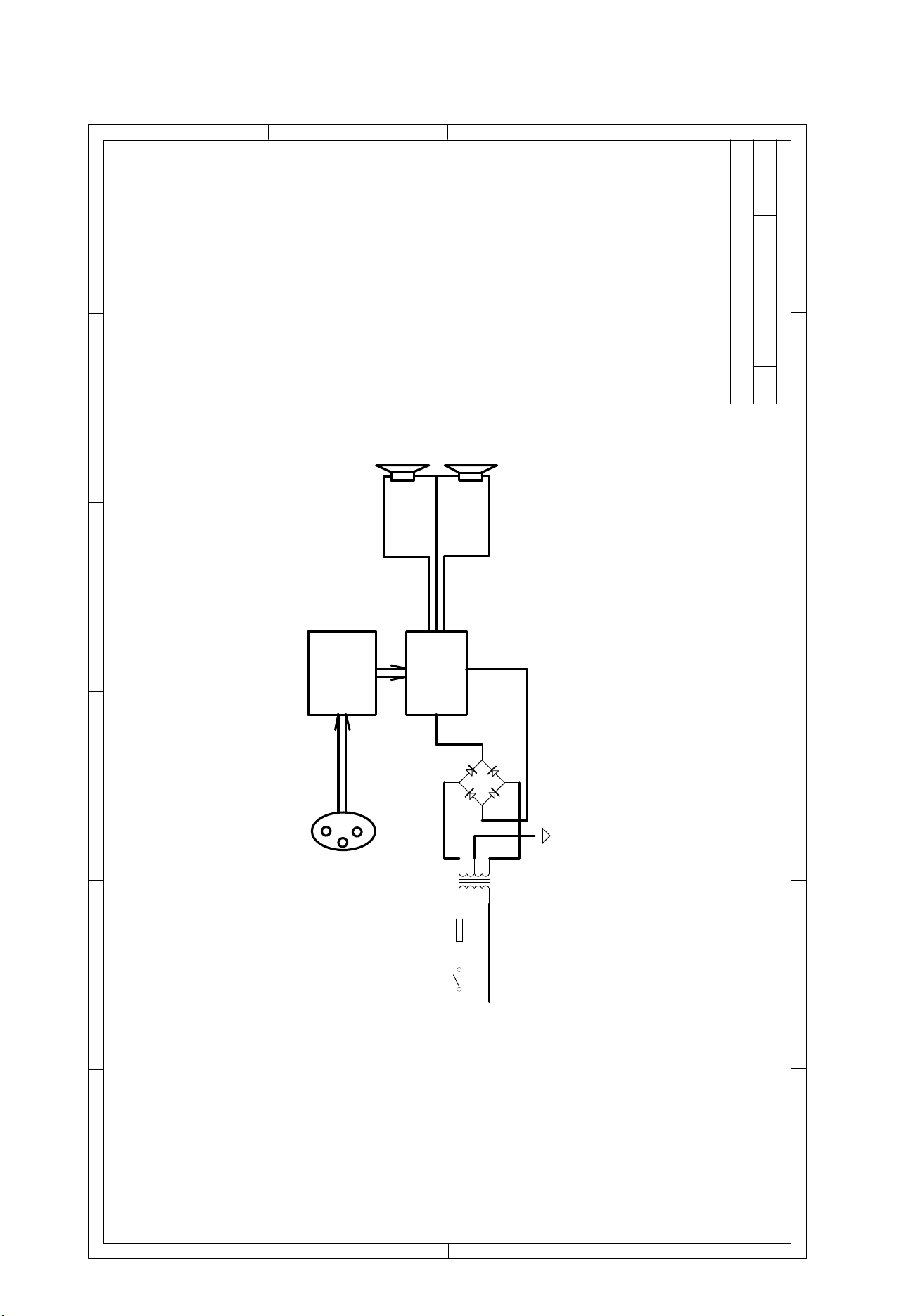
5. Wiring Diagram
9
Amp module
C
B
A
Number RevisionSize
PING LU TANG
B
Date: 3-Feb-2005 Sheet of
File: PBM4 Drawn By:
654321
PBM4 WIRING DIAGRAM
Title
MX
PBM4 WIRING DIAGRAM
IN/OUT
2
D1
1
T1
F1
S1
BRIDGE1
3
4
TRANS4
FUSE1
SW-SPST
AC 230V
1 2 3 4 5 6
D
C
B
A
Page 11
0
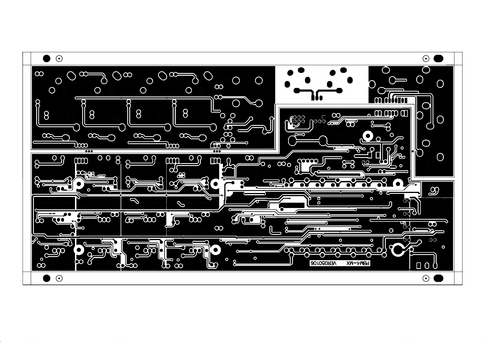
6. PCB Layout
(1) PCB: PBM4-MX BOTTOM LAYER
PCB: PBM4-MX BOTTOM LAYER
10
0
0
0
00
00 0
000
0000
0
0
Page 12

PCB: PBM4-MX BOTTOMOVERLAY
11
Page 13

0
PCB: PBM-MX TOP LAYER
12
0
0
0
0
0
00
0
0
0000
0
0
0
0
0
0
0
0
0
0
0
0
0
00
00
0
0
0
0
0
0
0
0
0
0
0
0
0
0
0
0
000
0
0
0
00
00
0
0
0
0
0000 0
0
0
0
0
0
0
0
000000
00
00
0
0
00
0
00
0
0
0
0
0
0
000
0
0
000
0
0
0
00
0 0
0000
000
0
0
00
0
0
0
0
0
0
0
0
0
0
0
0
0
0
0
0
0
0
0
0
0
0
00
0
0
0
0
0
00
00
00
0
0
0
0
0
0
0
0000000
0
0
0
0
0
0
0
0
0
0
00
0
000
00
0
0000
0
0
0
0
0
0
0
0
0
0
0
0
0
0
0
0
0
0
0
0
0
0
0
0
0
0
0
0
0
0
0
0
0
0
0
0
0
0
0
0
0
0
0
0
0
0
0
0
0
0
0
0000000
0
0
0
00
00
00
0
0
0
0
0
0
0
0
0
0
0
0
0
0
0
0
00
0
0
0
0
0
0
0
0
0
0
0
0
0
0
00
0
0
0
0
0
0
0
00
0
0
00
0
0
00
0
00
0 0
0
0
0
0
0
000
0
0
0
0
0
0
0
0
0
0
0
0
00
00
0
0
0
0
0
0
0
0
0
0
0
0
0
0
0
0
0
0
0
00
00 0
0
000
0
0
00
0
0
0
000
0
0
000
0
0
0
0
0
0
00
0
00
0
0
0 0
0
0
0
0
0
0
0
0
0
0
0
0
0
0
0
0
00
00
0
00
0
00
00
00
0
0
00
0
0
00
00000
0
0
0
0
0
0
0
0
0
0 0
0 0
0
0
0
0
0
0
00
0
00 00 00
0
00
0
0
0
0
0000000
0
0
0
0
0
0
0
0
0
00
000
0
0
0
0
0
0
0
0 0
0
0
0
000
0
0
0
0
0
0
0
0
0
0
0
0000000
0
0
0
0
0
0
0
0
0
0
0
0
0
0 00
0
0
0
0000
0
0
0
0
0
0
0
0
0
0
0
0
0
0
0
0
0
0
0
0 0
0
00
0
0
0
00
0
0
0
0
0
0
0
0
0
0
0
0
0
0
0
0
0
0
0
0
00
0
0
0
0
0
0
0
0
0000
0
0
0
0
000
0
0
0
0
0
0
0
00
0
0
0
0
0
0
0
00
000
0
0
0
0
0
0
00
0
0
0
0
0
00
0
00
0
0
0
0
0
0
0
0
0
0
0
0
00
0
0
0
0
0
0
0
0
0
0
0
0000
0
0
0
0
000
0
0
0
00
0
0
00
0
0
00
0
0
00
0
0
0
0
0
0 00
0
0
00
00
0
0
0
0
0
0000
0
0
0
0
0
0
0
0000
0
0
000
00
0
0
0
0
0
0
Page 14

PCB: PBM-MX TOPOVERLAY
13
Page 15

(2) PBM4-AMP
PCB: PBM4-AMP BOTTOM LAYER
PCB: PBM4-AMP BOTTOMOVERLAY
14
Page 16

PCB: PBM4-AMP TOP LAYER
PCB: PBM4-AMP TOPOVERLAY
15
Page 17

(3) 313123/2
PCB: 313123/2 TOP LAYER
PCB: 313123/2 BOTTOM LAYER
PCB: 313123/2 TOPOVERLAY
16
Page 18

OFF
7. Test Procedure
17
A
Number RevisionSize
PBM4
B
Title
Date: 3-Feb-2005 Sheet of
File: PBM4 Drawn By:
D
654321
C
VOL
AUX
2A
Load OUT
Load Sel
20A
4 8 16
DCIN
DCUT
~V A
AC
AMPERAS
888888 888888
B
AC220-240V
FUSE 2A
CH1=L
CH2=H
CH1 CH2
110 220
SHORT UNSWITCH
NOR.L NOR.L AC
110V
ON
SP2/OUT
220V
OFF
SP1/OUT
INPUT
PBM4
7724
D
Oscillograph
OUTPUT INPUT
1 2 3 4 5 6
C
B
A
Page 19

1. Instruments
18
(1) AP (Audio precision)
(2) Dual track Oscillograph
(3) DMM
2. Set up
(1) AP output: 0dBu 1KHz SINE(sine wave), load out 600Ω Bal-Float.
(2) AP input: Load 100KΩ BNC-Unbal. BW: 22Hz~22KHz. Fltr: A-weighting(12017)
3. Visual check
Inspect the appearance of PBM4. Ensure it is ok; the knob of the potentiometer should be no friction.
4. Test function
(1) Test the Phantom power
The power indicator lights up when you switch on PBM4. Set PHANTOM power switch to ON position.
The black pen of DMM connect to the first hole of MIC jack and respectively test CH1~CH4 of MIC
jack with DMM. The red pen of DMM respectively test the second hole and the third hole, the voltage
is 15V±2V. Set the switch to OFF position after finishing testing.
(2) Set PBM4
Turn all knobs to the middle position and turn all LEVEL knobs correspond to CH1~CH4 to the
maximum. Turn off DSP, the MAIN OUT indicator lights up when the AP signal input from LINE IN jack
of each channel; Set the AP output balanced when you test.
(3) Test DF/FX knobs for the output signal(CH1~CH4), MONITOR knobs and MAIN LEVEL
A. Set LEVEL knobs of CH1~CH4 to the maximum.
MAIN OUT: 3dBu(±3dBu), distortion <0.05%. Adjusting LEVEL knob, the output should be
changed accordingly.
MONTOR OUT LEFT: 8dBu(±3dBu), distortion <0.05%. Adjusting MONITOR knob, the output
should be changed accordingly.
FX SEND: 3dBu(±3dBu), distortion <0.003%. Adjusting DSF/FX knob of each channel, the
output should be changed accordingly
TAPE OUT: 3dBu(±3dBu), distortion <0.05%.
B. Set LEVEL knobs of CH1~CH4 to the minimum.
MAIN OUT: About -60dBu, it should be no signal output.
MONTOR OUT LEFT: About –70dBu(±3dBu), it should be no signal output.
FX SEND: About -70dBu(±3dBu), it should be no signal output.
TAPE OUT: About –70dBu(±3dBu), it should be no signal output.
C. Set the LEVEL knobs to the middle position
Page 20

MAIN OUT: –7dBu(±3dBu ), distortion <0.05%.
19
MONTOR OUT LEFT: -2dBu(±3dBu), distortion <0.05%
FX SEND: –7dBu(±3dBu), distortion <0.003%
TAPE OUT: –7dBu(±3dBu ), distortion <0.05%
(4) Test the output signal of CH5/6, when input mono signal to LEFT IN.
A. Set the LEVEL knobs of CH5~CH6 to the middle position
MAIN OUT: –21dBu(±3dBu ), distortion <0.1%.
MONTOR OUT LEFT: -16dBu(±3dBu), distortion <0.1%
FX SEND: About -70dBu(±3dBu )
TAPE OUT: –21dBu(±3dBu ), distortion <0.1%
B. Set LEVEL knobs of CH5~CH6 to the minimum.
MAIN OUT: About -60dBu(±3dBu), it should be no signal output.
MONTOR OUT LEFT: About –70dBu(±3dBu), it should be no signal output.
FX SEND: About -70dBu(±3dBu), it should be no signal output.
TAPE OUT: About –70dBu(±3dBu), it should be no signal output.
(5) Test the function of FX RETURN input and AUX/DFX RET knob.
A. Switch on DSP, set the AUX/DFX RET to the maximum
MAIN OUT: -29dBu(±3dBu), distortion <0.2%. Adjusting LEVEL knob, the output should be
changed accordingly
MONTOR OUT LEFT: -23dBu(±3dBu), distortion <0.2%. Adjusting MONITOR knob, the output
should be changed accordingly.
FX SEND: About -72dBu(±3dBu)
APE OUT: -29dBu(±3dBu), distortion <0.2%.
B. Switch on DSP, set the AUX/DFX RET to the minimum
No signal output on each channel
C. Switch on DSP, set the AUX/DFX RET to the middle position
MAIN OUT: -34dBu(±3dBu), distortion <0.3%.
MONTOR OUT LEFT: -29dBu(±3dBu), distortion <0.3%.
FX SEND: About -72dBu(±3dBu)
TAPE OUT: -35dBu(±3dBu), distortion <0.3%.
(6) Test the indicator of output level for MAIN OUT
Set the level of output signal for AP TO 10dBu. Connect the signal input of AP with MAIN OUT.
Set MAIN LEVEL from the minimum to the maximum. Inspect the output level on the computer during test,
the level that displays on the indicator of unit is in accordance with the level that displays on the computer.
The error is ±2dBu, the indicators light up in sequence from low to high. Don’t make mistake.
(7) Test the function of PAD switch, MIC jack, DSP switch, FOOT SW and DSP.
Page 21

A. Input the signal of 1KHz,-20dBu from MIC jack with Balanced. Output level data is similar to
20
LINE IN input .
B. When press the DSP switch, MUTE CHIP lamp should be up or down. Connect FOOT switch.
MUTE CHIP should be up or down.
C. DSP is switched on when the red lamp is down.
D. Adjust AUX/DFX RET knob to the minimum and adjust PRESETS switch. The wave on the
oscillograph stays the same.
(8) Test the EQ of CH1~CH4
A. Respectively Input signal 0dBu, 1KHz to LINE IN of CH1~CH4, adjust LEVEL of corresponding
channel to make MAIN OUT is 0dBu.Turn the EQ of HIGH and LOW for corresponding channel to the
middle position. Scan the curve of FREQUENCY RESPONSE. Refer to the yellow curve for the result.
B. Turn the HIGH EQ knob of corresponding channel clockwise to the maximum and turn the LOW
EQ knob counterclockwise to the minimum. Scan the curve of FREQUENCY RESPONSE, refer to the
purple curve for the result.
C. Turn the HIGH EQ knob of corresponding channel counterclockwise to the minimum and turn the
LOW EQ knob clockwise to the maximum. Scan the curve of FREQUENCY RESPONSE, refer to the
red curve for the result.
For the test above, the error of the curve range is ±3dBu.
Page 22

Turn the EQ knob of all channels to the middle position after finishing test.
21
(9) Test the curve of MAIN EQ
A. Respectively input signal 0dBu, 1KHz to a channel from CH1~CH4. Set all slide potentiometers
of MAIN EQ to the middle position. Adjust LEVEL of the corresponding channel to make MAIN ON is
0dBu. Connect the input terminal of AP to MAIN OUT LEFT and MAIN OUT RIGHT. Scan the curve of
FREQUENCY RESPONSE, refer to the yellow curve for the result.
B. Set the slide potentiometer 63, 400, 2.5K, 16K to the top
Set the slide potentiometer 160, 1K, 6, 3K to the bottom.
Scan the curve of FREQUENCY RESPONSE, refer to the red curve for the result.
C. Set the slide potentiometer 63, 400, 2.5K, 16K to the top.
Set the slide potentiometer 160, 1K, 6, 3K to the bottom.
Scan the curve of FREQUENCY RESPONSE, refer to the red curve for the result.
D. For the test above, the error of the curve range is ±3dBu.
Turn the EQ of all channels to the middle position after finishing test.
(10) Test listening
Respectively input the music signal of proper level to all signal input terminals. Connect the unit
output with power amplifier and connect MONIOR OUT with headphone. Set all potentiometers related
to this channel from the minimum to the maximum when you test the input and output of each channel,
Page 23

repeat twice or thrice, eliminate unwanted noise during test and the output should be changed
22
accordingly. Turn on/off the switch twice, it should be no noise.
Company preset: Turn all LEVEL knobs to the minimum. Set the PHANTOM switch to OFF position and
other knobs to the middle position.
Page 24

50 Hz
SEKAKU ELECTRON INDUSTRY CO., LTD. PAGE: 1
23
Test Result JFM-1006-5.0
Test Date: 2005/01/17Model No:PBM4-AMP
Test Item
1 Power Source
Motionless State
2
3
4
5 __________W FLAT
Current
Power
Consumption
Rated Output Load 4Ω __V _______V
Maximum at Output 10% THD
Rated Output. Aux At 1KHz
CHAN1 1Hz_-3.7±0.3dB Load__8__Ω
Test Conditions
AC: 240 V;
DC______V Load_____Ω
Load 8Ω _21.9V±1V _______V
Load 16Ω __V _______V
Load ____Ω(25V)
Load____Ω(50V) _______V _______V
Load____Ω(70V) _______V _______V
Load____Ω(100V) _______V _______V
Spec Test Result Remark
________A
_______A _______A
_______W _______W
_______V _______V
_60_W
________A
CHAN1 At 1KHz FLAT.
Rated __w OUTPUT
VR knob turn to the
FLAT
Hum or Noise VR Max (Tape On) __↓__mV ________mV
6
VR Max (Tape Off ) __↓__mV ________mV
Tone control Response
7
8 Puncture Voltage
MONITOR
MONITOR NO:
TAPE
TUNER
PRIORITY
9
TEL.PAGING ma G-T___dB;G-R___dB。
ZONE PAGING ALL/ Z1, Z2, Z3, Z4
AC : OUTPUT
Input From CHAN1 Output At 1W 100HZ:_-±1dB 100HZ:______dB
10KHZ:_-±1dB 10KHZ:______dB
5mA , 60Sec
Aux 1KHz____dB Load____Ω
AUX1、2,TAPE,TUNER。
6.3KHz -10dB
AM/FM
MIC1
1KHz____dB Load____Ω_______V
100V
1200V或4000V
、2,TAPE,TUNER。
2500V
FLAT
MAX
MAX
FLAT
REMOTE
AC OUT OR DC OUT
Page 25

SEKAKU ELECTRON INDUSTRY CO.,LTD PAGE: 2
Test Result JFM-1006-5.0
Model No:PBM4
Test Date:2005/01/17
Tester
24
Test Item
Test Conditions
Test Result
AUX1
AUX2
AUX3
MIC-1
MIC-2
MIC-3
MIC-4
MIC-5
Remark
1. Input Sensitivity 2. Signal/Noise 3. Distortion at 1W
FLAT Rated
Output_60_w
Load__8__Ω
AUX dB dB % %
TAPE dB dB % %
TUNER dB dB % %
CD dB dB % %
AUX dB dB % %
TAPE dB dB % %
TUNER dB dB % %
CD dB dB % %
AUX dB dB % %
TAPE dB dB % %
TUNER dB dB % %
CD dB dB % %
MIC dB dB % %
SEND dB
CH1 -3.7dB±0.3dB
CH2 -3.7dB±0.3dB
MIC dB dB % %
LINE dB dB % %
24V dB dB % %
UNBAL dB dB % %
MIC dB dB % %
LINE dB dB % %
24V dB dB % %
UNBAL dB dB % %
MIC dB dB % %
LINE dB dB % %
24V dB dB % %
UNBAL dB dB % %
MIC dB dB % %
LINE dB dB % %
24V dB dB % %
UNBAL dB dB % %
1.Input at 1KHz
FLAT Rated
Output__60__w
Load__8__Ω
dB↑ %↓ %↓
85dB↑
85dB↑ 0.2%↓ 0.15%↓
FLAT Output
at 1w Load__8__
Ω
0.2%↓ 0.15%↓
4. Distortion at
Rated
FLAT Rated
Output__60_w
Load__8__Ω
:
5. Frequency
Response
FLAT Output at 1w
REF -3dB
Load__8__Ω
HZ↓-KHZ↑
44HZ↓-30KHZ↑
44HZ↓-30KHZ↑
HZ↓KHZ↓
Page 26

8. Exploded Views & Mechanical Part List
25
Page 27

S/N Part No. Description Specification Qty
26
1 NI03241 Panel 318*194*30 black_V1.0 1
2 NI01957 Rear cover PAM5 1
3 MG00550 Screw M4*35 8
4 MG00370 Screw M8*14.2*1.25PH 2
5 ME00094 Nut M8*1.25PH 4
6 MF00097 Washer
φ32*φ9*2t PAM-5
4
7 MG00387 Screw M3*20 6
8 MG00051 Screw M3*16 10
9 HK05013 Panel PBM4-MX 1
10 HK05111 Panel PBM4_230V 1
11 MG00465 Screw M8*9.5*1.25PH 2
Page 28

27
Page 29

28
Page 30

No. Part No. Description Specification Remark
9. BOM
29
1 NI03636 panel PBM4_V1.0
2 NI03241 panel 318*194*30 black_V1.1
3 NI01957 rear cover PAM5
4 NI02576 rear cover PAM5 black
5 MG00550 screw M2.6*8
6 MG00370 screw M8*14.2*1.25PH
7 ME00094 nut M8*1.25PH
8 MF00079 washer
9 MF00078 washer
10 MJ01154 single light board 2.0t*1850*950mm 27.6kg
11 MG00387 screw M3*20
12 NE11750 label ALTO PC
13 NH00334 cone paper 0.040*1m
14 NE05966 label PBM4_V1.0
15 NH00012 bond paper 0.04*1M
16 NI00014 membrane 0.035*1M
17 MG00051 screw M3*16
18 NF00061 assurance card ALTO
19 NA00125 PE bag 0.04t*580*400mm
20 NB03358 gift carton PBM4 ALTO_V1.0
21 NB03246 carton PAM5;PAM5A;PAM5T_V1.0
22 NB03374 cushion PBM4 down_V1.0
23 NB03375 cushion PBM4 up_V1.0
24 HJ00006 desiccant 30g
25 HK05013 faceplate PBM4-MX
26 MA05457 panel PBM4 ALTO_V1.0
27 MA05454 panel PBM4
28 MA05453 panel PBM4 1.0t*162.4*293.4_V1.1
29 MJ00058 single light board 1*2135*1220 20.45kg
30 MG00248 copper pillar M3*15*0.5PHdouble plane
31 MG00041 screw M3*6
32 MG00061 screw M3*10
33 ME00060 MIC jack JY-6351G-02-250
34 MF00061 MIC jack
35 NI00359 knob
36 NI00399 knob
37 NI02386 knob
38 NI02252 knob cover
39 NI02100 knob cover
40 NI02677 knob cover
41 HA03810 wire
42 HK05038 PC board P-PBM4-MX-DIP
43 HC00079 connector(male) 5P 2.5mm 180° CN9
44 RA00125 fixed resistor 1/2W
45 CB00217 electrolytic capacitor
46 HI00246 slide switch 2 stages 6P SS-22H23-G14(2P2T) SW1
47 SD00074 integrated circuit L7805CV(TO-220)(ST) TR2
φ32*φ9*2t PAM-5
φ32*φ9*2t PAM-5
φ9.6*φ13*0.5t
φ10*16.5
φ11*19mm
φ14*13mm
φ7*3.5 072C
φ7*3.5 222C
φ8.5*4 534C blue
10P-3P/5P 400mm UL1007 24AWG red/white
470Ω M type
470uF/50V φ10*20mm
R181
C146
Page 31

No. Part No. Description Specification Remark
C20,C47,C48,C49,C50,C51,C52,C53,C54,C55,C56,C57,
C140,C141,C142,C1,C2,C3,C4,C5,C6,C126,C138,C139,
C80,C81,C82,C83,C84,C85,C86,C87,C88,C89,C90,C91,
C92,C93,C94,C95,C96,C97,C98,C99,C100,C101,C102,
R24,R25,R26,R27,R28,R29,R30,R31,R34,R38,R43,R44,
30
48 RA00181 fixed resistor 1/4W
49 RC00358 potentiometer
50 HI00195 rotary switch SDB161PVB15.5F-1-4-16-16PC SW2
51 HA02199 wire
52 HC00257 connector(male) 6P 2.0mm 180° CN1,CN3,CN10
53 HC00397 connector(male) 10P 2.0mm 180° CN6
54 HA01582 wire
55 HC00077 connector(male) 3P 2.5mm 180° CN12
56 SA00052 L.E.D
57 HC00499 connector 2.54 180°2*8P(gold-plated) 6/11.6mm CN8
58 HC00126 balance MIC jack JY-5042-030G female plug 180° J1,J3,J5,J17
59 HI00238 push-button switch-RS 2 stage 6P PS-9226A(NON-LOCK) SW3
60 HC00403 RCA jack SCP6873NS3232T2 4P J7
61 SA00053 L.E.D
62 HC00371 MIC jack SCJ-0658-1-Y J2,J4,J6,J8,J9,J10,J15,J16,J18,J19
63 RC00462 slide potentiometer
64 RC00359 potentiometer
65 SA00054 L.E.D 3m/m round(yellow)long foot 26 D7
66 NI01786 LED spacer support LEDS-12 12mm
67 HK05039 PC board P-PBM4-MX-AI
68 RA01112 fixed resistor 1/4W
69 CB00235 electrolytic capacitor
70 CB00263 electrolytic capacitor
71 CB00189 electrolytic capacitor
72 CB00196 electrolytic capacitor
73 RA01117 fixed resistor 1/4W
82Ω M type
B50KΩ-RD09F113A223-50K2BT(SAS1);30F-C
6P(male)-6P(female) 70mm(AWG26 UL1007)
10P(male)-10P(female) 60mm UL1007 28AWG
φ3 round(green)long foot 26
φ3 round(red)long foot 26mm
W100KΩ RA3072-20-085EB-W100K-C
W50KΩ RD09F113A224-50K4BT(SAS1);30F-C
100Ω
100uF/25V φ6*11mm
10uF /25V φ4*7mm
1.0uF/50V φ4*5mm
220uF/16V φ8*11mm
22Ω
R33
VR1,VR2,VR5,VR6,VR9,VR10,VR13,VR14,VR20
CN2,CN4,CN11
CN5
D5,D6,D9
D8,LD1
RF1-7,RF2-7,RF4-7,RF5-7, RF6-7,RF8-7,RF9-7
VR3,VR4,VR7,VR8,VR11,VR12,VR15,VR16,VR21,VR22
R32,R149,R150
C135
C133,C147
C129,C132
C148
R134,R133
C7,C8,C9,C10,C11,C12,C13,C14,C15,C16,C17,C18,C19,
74 CB00194 electrolytic capacitor
75 CB00249 electrolytic capacitor
76 CB00264 electrolytic capacitor
47uF/25V φ5*11mm
47uF/50V φ6.3*11mm 2.5mm
4.7uF/63V NP φ6.3*11mm 5mm
77 HK05040 PC board P-PBM4-MX-SMD
78 HB01477 PCB PBM4-MX_VER050106
79 RD00059
80 RD00116
81 CI00075
82 CI00059
83 RD00101
84 CI00071
85 CI00047
86 RD00061
87 RD00102
88 RD00103
89 RD00071
90 RD00104
91 RD00083
SMD fixed resistor 1/10W 0.0Ω ±5% 0603
SMD fixed resistor 1/10W 100KΩ ±5% 0603
SMD ceramic capacitor 0603
SMD ceramic capacitor 0603
SMD fixed resistor 1/10W 10KΩ ±5% 0603
SMD ceramic capacitor 0603
SMD ceramic capacitor 0603
SMD fixed resistor 1/10W 10Ω ±5% 0603
SMD fixed resistor 1/10W 12KΩ ±5% 0603
SMD fixed resistor 1/10W 15KΩ ±5% 0603
SMD fixed resistor 1/10W 180Ω ±5% 0603
SMD fixed resistor 1/10W 18KΩ ±5% 0603 RF1-5,RF2-5,RF4-5,RF5-5,RF6-5,RF8-5,RF9-5
SMD fixed resistor 1/10W 1.0KΩ ±5% 0603
0.1uF/50V Y5V +80,-20%
100PF/50V NPO ±5% C76,C77
0.01uF/50V X7R ±10% CF5-1,CF5-2,CF6-1,CF6-2
10PF/50VC0G±0.25PF(C1608C0G1H100C
T)TDK
C58,C59,C60,C61,C62,C63,C64,C65,C74,C75,C124,
C143,C144,C145
C122
R162
R51,R139,R140,RF8-3,RF8-4,RF8-1
C103,C104,C105,C106,C107,C108,C109,C110,C111,
C112,C113,C114,C115,C116,C117,C125,C128,C131,C136
,C137
R7,R8,R9,R10,R11,R12,R13,R14,R15,R16,R21,R22,R23,
R126,R166,R175
C118,C134
R152
R135,R154
RF1-1,RF1-3,RF1-4
R146
R74,R75,R76,R77,R78,R79,RF6-2,R167
Page 32

No. Part No. Description Specification Remark
31
92 RD00084
93 RD00085
94 RD00086
95 RD00125
96 CI00065
97 CI00129
98 RD00119
99 CI00179
100 RD00073
101 RD00105
102 CI00051
103 RD00106
104 RD00088
105 RD00089
106 RD00126
107 RD00353
108 RD00109
109 RD00090
110 RD00091
111 RD00092
112 RD00026
113 CI00069
114 SG00122 SMD integrated circuit NJM4580M-TE3
115 SG00200 SMD integrated circuit NJM4580V-TE1/(JRC) UF2,UF3,UF4
116 RD00111
117 RD00093
118 CI00056
119 RD00094
120 RD00095
121 RD00080
122 RD00097
123 RD00513
SMD fixed resistor 1/10W 1.2KΩ ±5% 0603
SMD fixed resistor 1/10W 1.5KΩ ±5% 0603
SMD fixed resistor 1/10W 1.8KΩ ±5% 0603
SMD fixed resistor 1/10W 1.0MΩ ±5% 0603 R105,R106,R107,R108,R109,R110, R111,R156
SMD ceramic capacitor 0603
SMD ceramic capacitor 0603
SMD fixed resistor 1/10W 220KΩ ±5% 0603
SMD ceramic capacitor 0603
SMD fixed resistor 1/10W
SMD fixed resistor 1/10W
SMD ceramic capacitor 0603
SMD fixed resistor 1/10W
SMD fixed resistor 1/10W
SMD fixed resistor 1/10W 2.7KΩ ±5% 0603
SMD fixed resistor 1/10W 2.2MΩ ±5% 0603
SMD fixed resistor 1/10W 36KΩ ±5% 0603
SMD fixed resistor 1/10W 39KΩ ±5% 0603
SMD fixed resistor 1/10W 3.0KΩ ±5% 0603
SMD fixed resistor 1/10W 3.3KΩ ±5% 0603
SMD fixed resistor 1/10W 3.9KΩ ±5% 0603
SMD fixed resistor 1/8W 3.9KΩ ±5% 0805
SMD ceramic capacitor 0603
SMD fixed resistor 1/10W 47KΩ ±5% 0603
SMD fixed resistor 1/10W 4.7KΩ ±5% 0603
SMD ceramic capacitor 0603
SMD fixed resistor 1/10W 5.1KΩ ±5% 0603
SMD fixed resistor 1/10W 5.6KΩ ±5% 0603
SMD fixed resistor 1/10W
SMD fixed resistor 1/10W 6.8KΩ ±5% 0603
SMD fixed resistor 1/10W 2.4KΩ ±5% 0603
0.001uF/50V X7R ±10% CF8-1,CF8-2,CF9-1,CF9-2
0.0015uF/50V X7R ±10% C127
0.22uF/25V X7R±10%(C1608X
7R1E224KT)/TDK
220Ω ±5% 0603
22KΩ ±5% 0603
22PF/50V C0G±5%(C1608C0
G1H220JT)/TDK
27KΩ ±5% 0603
2.2KΩ ±5% 0603
0.0033uF/50V X7R ±10﹪
56PF/50V NPO ±5% C119,C120,C121
680Ω ±5% 0603
RF2-2
R129
RF4-2
R155
C130,CF1-1,CF1-2,CF2-1,CF2-2
R159,R160
R19,R35,R39,R45,R48,R50,R52,R53,R54,R55,R57,R58,
R61,R62,R67,R68,R70,R131,R171,R172,R176,RF6-1,
RF6-3,RF6-4
C21,C22,C23,C24,C25,C26,C27,C28,C29,C30,C31,C32
C33,C34,C35,C36,C37,C38,C66,C67,C68,C69,C70,C71,
C72,C73,C78,C79
R147,RF9-1,RF9-3,RF9-4
R56,R59,R60,R63,R64,R65,R66,R69,R72,R73,R170,
R173,R177,R178,R179,R180,RF9-2
R49,RF5-2
R158
R116,R117,R118,R119,R120
R130,R136,RF4-1,RF4-3,RF4-4
R80,R81,R82,R83
RF8-2
R97,R98,R99,R100,R101,R102,R103,R104
R151
C123
U1,U2,U3,U4,U5,U6,U7,U8,U9,U10,U11,U12,U13,U14,
U15,U19,U20
R127,R128,RF5-1,RF5-3,RF5-4
R157
R121,R122,R123,R124,R153,R163,R164
R71,R125,R137,R138,RF1-2
R20,R141,R142,R143,R144,R145
R17,R18,R84
R1,R2,R3,R4,R5,R6,R42,R165
124 SG00164 SMD integrated circuit 74HC109D U17
125 SG00068 SMD integrated circuit 74HC14DT(SO-14)/(PHI) U18
126 RD00098
127 RD00124
128 RD00099
SMD fixed resistor 1/10W 7.5KΩ ±5% 0603
SMD fixed resistor 1/10W
SMD fixed resistor 1/10W
820KΩ ±5% 0603
8.2KΩ ±5% 0603
R148
R161
R85,R86,R87,R88,R89,R90,R91,R92,R93,R94,R95,R96,
R112,R113,R114,R115,R174,RF2-1,RF2-3,RF2-4
129 SF00051 transistor SST176(S6)(SOT-23)/(VISHAY) TR1
130 SG00094 SMD integrated circuit NE555DT/(ST) U16
131 SE00011 SMD rectifier diode RLS4148 0.5A (LL-34) D1,D2,D3,D4,D10,D11,D12,D13
132 AE00221 tin soldering paste SJ-617
133 RD00068
134 CI00148
SMD fixed resistor 1/10W 100Ω ±5% 0603
SMD ceramic capacitor 0603
0.033uF/50V X7R±10%(C1608X
7R1H333KT)TDK
R46,R47
CF4_1,CF4_2
Page 33

No. Part No. Description Specification Remark
32
135 AC00002 solder wire 63/37%
136 RC00429 potentiometer
137 NI01627 fixed bracket CM-19S
138 NI00218 cable tie ALT-102SB
139 HA00370 wire 80mm black L5R5
140 HK05010 PC board P-313123-DIP(PBM4)
141 SC00004 crystal oscillator 16.00MHZ XT1
142 HC00499 connector 2.54 180°2*8P(gold-plated) 6/11.6mm CN2
143 SG00325 SMD integrated circuit
144 SG00139 SMD integrated circuit AT27LV010A-90JC
145 HK03894 PC board P-313123-SMD(L-8)
146 HB00895 PCB 313123/2(1*6)
147 CI00049
148 CI00075
149 RD00061
150 RD00068
151 RD00073
152 RD00085
153 RD00088
154 RD00101
155 RD00125
156 RE00006
SMD ceramic capacitor 0603
SMD ceramic capacitor 0603
SMD fixed resistor 1/10W 10Ω ±5% 0603
SMD fixed resistor 1/10W 100Ω ±5% 0603
SMD fixed resistor 1/10W 220Ω ±5% 0603
SMD fixed resistor 1/10W 1.5KΩ ±5% 0603
SMD fixed resistor 1/10W
SMD fixed resistor 1/10W 10KΩ ±5% 0603
SMD fixed resistor 1/10W 1.0MΩ ±5% 0603
SMD resistor networks 1/16W
157 SE00011 SMD rectifier diode RLS4148 0.5A (LL-34) D1
B10KΩ RK09K113Z11110K2B(SAS1);30F-C
AT27LV010A-90JC/OEX600 CE:E1880
15PF/50V C0G±5%(C1608C0
G1H150JT)/TDK
0.1uF/50V Y5V +80,-20%
2.2KΩ ±5% 0603
100Ω*4 ±5% 8P 0603
VR17
C8,C9
C17,C15,C18,C6,C10,C22,C20,C13,C14,C1,C3,C4,C11
R22
R12,R14,R7,R8,R34,R17,R13,R33
R3
R16,R15,R21,R20,R4,R19,R10,R18,R9,R5
R28,R27,R23,R24,R29,R30,R25,R26
R32,R31,R1
R2
AR1,AR2
158 SG00068 SMD integrated circuit 74HC14DT(SO-14)/(PHI) IC1
159 SG00410 SMD integrated circuit IC41LV16256-35KG(SOJ40)/(ICSI) IC6
160 SG00166 SMD integrated circuit TY-2 ALTO(GMCODE:105022) IC3
161 SG00147 SMD integrated circuit CHEF DSP(GMCODE:105022)
162 SG00037 SMD integrated circuit LD1117DT33C(TO-252) IC2
163 HC00233 IC socket (PCB) PLCC32 (D03-32T.A.4) IC4
164 SG00016 SMD integrated circuit UDA1345TS (Philips) IC5
165 AE00221 tin soldering paste SJ-617
166 AC00002 solder wire 63/37%
167 NE04154 label OEX600_V1.0
168 NH00035 bond paper 0.06*1M
169 NI00017 membrane 0.055*1M
170 CB00166 electrolytic capacitor
100uF/16V φ6*5mm C19,C12,C5,C2,C24,C16,C21,C25,C26,C28,C7
171 MJ00487 heat-sink PBM4 1.5t*67*142_V1.0
172 MJ00092 AL plate-RS 1.5*2000*1000 8.16kg
173 ME00180 iron pillar
6.35*φ3.5*6_V1.0
174 ME00134 iron pillar M3*2.8*0.5PH
175 NI02620 insulation board 1*86.5*53 L-8
176 NC00010 insulation board 0.65M*60M*1t
177 NI02249 plastic washer TW-1(TO-220)
178 NC00005 silicone insulator TO-220 square type
Page 34

No. Part No. Description Specification Remark
33
179 MG00518 screw M3*7*0.5PH
180 MG00377 screw M3*16mm
181 MG00027 screw M3*12
182 MF00037 washer
183 HA03811 wire
184 MG00248 copper pillar M3*15*0.5PHdouble plane
185 CF00008
metal-film capacitor MSC
186 NI02957 knob 9.8*5.5*11.2mm black_V1.0
187 HK05111 PC board PBM4_230V
188 MA05448 panel
189 MA00440 panel PBM4S 4.0t*242.5*95.5
190 MA00437 panel PBM4S 4.0t*242.5*95.5_V1.2
191 MJ00218 panel 4.0t*242.5*95.5 PAM5A
192 HI00021 power switch 4P6A
193 TD00427 transformer PT-PBM4_230V
194 HA02490
power cord(European 3P)
195 NI00558 bushing SBR5-1
196 HC00060 FUSE holder
197 NI02603 plastic nut
φ3.2*φ5.5*1t
16P-16P 90mm UL2651 28AWG red/gray
0.0047uF/100V 5% CASE01 C39,C40,C41,C42,C43,C44,C45,C46
PBM4 230V 50/60Hz CHINA ALTO_V1.2
LT-312+0.75*3C(H03VV-F)2.5M
φ12.4*11.8
φ6
198 MI02503 heat sink PBM4S 10.8*76.2*140 0.103Kg_V1.0
199 MG00041 screw M3*6
200 MI02527 fixed bracket PBM4S 105*85*41*1.5t_V1.1
201 MJ00069 iron board 1.5*2135*1220 30.67kg
202 NI00442 rubber coil
φ20*φ85*2tB
203 ME00130 nut M6*1.0PH
204 MF00040 washer
205 MF00053 washer
φ6*φ10*1.5t
φ6.3*φ16*1t
206 MG00466 screw M4*8*0.7PH
207 ME00015 color nut 3m/m
208 MF00037 washer
φ3.2*φ5.5*1t
209 MG00389 screw M4*16*0.7PH
210 MF00048 washer
211 MF00038 washer
φ4*φ8*0.5t
φ4*φ7*1t
212 ME00016 color nut 4m/m
213 HK04705 PC board P-PBM4-AMP
214 HB01439 PCB PBM4-AMP_VER050427
215 CF00035
metal-film capacitor MPX
0.1uF/275V C36
216 SA00009 bridge rectifier BU10-04 10A/400V BR1
217 HC00324 connect terminal 6.5m/m (PC250) AC1,AC2,GND
218 MI00256 heat-sink 25*15*10.6-1PIN SCL-2020 U6,U3
219 MI00208 heat-sink(black) 26.5*28*9 BR1
220 NI00863 plastic washer TO220B U6,U3
221 NC00005 silicone insulator TO-220 square type U6,U3
222 MG00163 screw M3*8 U6,U3
223 MG00170 screw M3*14 BR1
Page 35

No. Part No. Description Specification Remark
34
224 ME00015 color nut 3m/m BR1
225 MF00037 washer
226 CB00125 electrolytic capacitor
227 CB00287 electrolytic capacitor
228 CB00095 electrolytic capacitor
229 SA00098 rectifier diode 1A/400V IN4004 D3,D4,D5,D6
230 SA00102 zener diode 1W 7.5V 1N4737 D1,D2
231 SB00073 transistor 2N5550/2N5551 Q1
232 SD00077 integrated circuit L7815CV(TO-220)(ST)(MOROCCO) U6
233 SD00079 integrated circuit L7915CV(TO-220)(ST) U3
234 SD00035 integrated circuit LM3886TF(NS) U1,U2
235 RA00480 precise resistor 1/4W
236 HC00084 connector(male) 10P 2.5mm 180° CN2
237 CB00009 electrolytic capacitor
238 CF00030
239 CB00041 electrolytic capacitor
240 CB00050 electrolytic capacitor
241 CB00063 electrolytic capacitor
242 RA00452 precise resistor 1/4W
243 RA00468 precise resistor 1/4W
244 RA00544 precise resistor 1/4W
245 RA00490 precise resistor 1/4W
246 RA00559 precise resistor 1/4W
247 RA00858 precise resistor 1/4W
248 HA01984 single terminal wiring 115mm
249 RA01438 chassis bracket 7W
250 RA01437 chassis bracket 7W
251 AC00002 solder wire 63/37%
252 MI02657 fixed bracket PBM4S 1.5t*80*50*15 Ltype_V1.1
253 MJ00069 iron board 1.5*2135*1220 30.67kg
254 ME00050 iron pillar M3*9.7
255 MG00598 screw M3*8_V1.0
256 MG00060 screw M3*6
257 HD00028 glass tube fuse
258 NI00252 sleeve
259 NI00248 sleeve
260 MG00364 screw M3*12mm
261 NI00218 cable tie ALT-102SB
262 MG00214
263 NE05267 label red
264 NH00025 bond paper 0.065*1M
265 NI00018 membrane 0.06*1M
266 MG00465 screw M8*9.5*1.25PH
267 NF02055 instruction PBM4 ALTO_V1.0
268 NH00231 paper 889*554mm
269 NE02717 label MADE IN CHINA
270 NH00038 paper 0.115*1M
271 NI00028 membrane 0.110*1M
metal-film capacitor MSC
outside hexagon screw
φ3.2*φ5.5*1t
470uF/35V φ10*20mm
1000uF/50V φ12.5*26mm 5mm
6800uF/50V φ25*40mm
2.21KΩ M type
1uF/50V φ4*7mm
0.1uF/63V 5% CASE01 C2,C4,C6,C7,C10,C12,C15,C17
47uF/50V φ6*11mm
100uF/50V φ8*11mm
330uF/16V φ8*11mm
100Ω M type
1.00KΩ M type
33.0KΩ M type
3.48KΩ M type
61.9KΩ M type
47.0KΩ M type
95Ω SQM type 5mm
200Ω SQM type 5mm
2A 250V φ5.2*20mm CSA/S/UL/VDE
φ4*20mm
φ4*1000mm
M6*65
BR1
C41,C31
C30,C37
C13,C35
R5,R7
C20
C9,C11,C18,C14
C1,C3,C5,C8
C19
R8
R4,R6
R1,R2
R16,R17,R18
R15,R19
R13
R3
R9
 Loading...