

Page 1

Santa Cruz, USB, MICTOR, SD Card HSMC
Reference Manual
101 Innovation Drive
San Jose, CA 95134
www.altera.com
Document Version: 1.0
Document Date: December 2008
Page 2

Copyright © 2008 Altera Corporation. All rights reserved. Altera, The Programmable Solutions Company, the stylized Altera logo, specific device designations, and all other
words and logos that are identified as trademarks and/or service marks are, unless noted otherwise, the trademarks and service marks of Altera Corporation in the U.S. and other
countries. All other product or service names are the property of their respective holders. Altera products are protected under numerous U.S. and foreign patents and pending applications, maskwork rights, and copyrights. Altera warrants performance of its semiconductor products to current specifications in accordance with Altera's standard warranty,
but reserves the right to make changes to any products and services at any time without notice. Altera assumes no responsibility or liability arising out of the application or use of
any information, product, or service described herein except as expressly agreed to in writing by Altera Corporation. Altera customers are advised to obtain the latest version of
device specifications before relying on any published information and before placing orders for products or services.
MNL-01040-1.0
Page 3

Contents
Chapter 1. Overview
General Description . . . . . . . . . . . . . . . . . . . . . . . . . . . . . . . . . . . . . . . . . . . . . . . . . . . . . . . . . . . . . . . . . . . . . 1–1
Board Component Blocks . . . . . . . . . . . . . . . . . . . . . . . . . . . . . . . . . . . . . . . . . . . . . . . . . . . . . . . . . . . . . . . . . 1–1
Block Diagram . . . . . . . . . . . . . . . . . . . . . . . . . . . . . . . . . . . . . . . . . . . . . . . . . . . . . . . . . . . . . . . . . . . . . . . . 1–2
Handling the Board . . . . . . . . . . . . . . . . . . . . . . . . . . . . . . . . . . . . . . . . . . . . . . . . . . . . . . . . . . . . . . . . . . . . . . 1–2
Chapter 2. Board Components
Introduction . . . . . . . . . . . . . . . . . . . . . . . . . . . . . . . . . . . . . . . . . . . . . . . . . . . . . . . . . . . . . . . . . . . . . . . . . . . . 2–1
Board Overview . . . . . . . . . . . . . . . . . . . . . . . . . . . . . . . . . . . . . . . . . . . . . . . . . . . . . . . . . . . . . . . . . . . . . . . . . 2–1
HSMC Connector (J1) . . . . . . . . . . . . . . . . . . . . . . . . . . . . . . . . . . . . . . . . . . . . . . . . . . . . . . . . . . . . . . . . . . . . 2–4
Santa Cruz Connectors (J3, J4, and J5) . . . . . . . . . . . . . . . . . . . . . . . . . . . . . . . . . . . . . . . . . . . . . . . . . . . . . . 2–7
USB On-The-Go Transceiver (U11) . . . . . . . . . . . . . . . . . . . . . . . . . . . . . . . . . . . . . . . . . . . . . . . . . . . . . . . . 2–11
MICTOR Connector (J2) . . . . . . . . . . . . . . . . . . . . . . . . . . . . . . . . . . . . . . . . . . . . . . . . . . . . . . . . . . . . . . . . . 2–13
SD Card Interface (J7) . . . . . . . . . . . . . . . . . . . . . . . . . . . . . . . . . . . . . . . . . . . . . . . . . . . . . . . . . . . . . . . . . . . 2–16
SMA Connector (J6) . . . . . . . . . . . . . . . . . . . . . . . . . . . . . . . . . . . . . . . . . . . . . . . . . . . . . . . . . . . . . . . . . . . . 2–17
2
I
C Serial EEPROM (U10) . . . . . . . . . . . . . . . . . . . . . . . . . . . . . . . . . . . . . . . . . . . . . . . . . . . . . . . . . . . . . . . . 2–17
Power Supply . . . . . . . . . . . . . . . . . . . . . . . . . . . . . . . . . . . . . . . . . . . . . . . . . . . . . . . . . . . . . . . . . . . . . . . . . . 2–18
Appendix A. Demonstration
Additional Information
Revision History . . . . . . . . . . . . . . . . . . . . . . . . . . . . . . . . . . . . . . . . . . . . . . . . . . . . . . . . . . . . . . . . . . . About–1
How to Contact Altera . . . . . . . . . . . . . . . . . . . . . . . . . . . . . . . . . . . . . . . . . . . . . . . . . . . . . . . . . . . . . . About–1
Typographic Conventions . . . . . . . . . . . . . . . . . . . . . . . . . . . . . . . . . . . . . . . . . . . . . . . . . . . . . . . . . . . About–1
. . . . . . . . . . . . . . . . . . . . . . . . . . . . . . . . . . . . . . . . . . . . . . . . . . . . . . . . . . . . . . . . . About–1
© December 2008 Altera Corporation Santa Cruz, USB, MICTOR, SD Card HSMC Reference Manual
Preliminary
Page 4

iv
Santa Cruz, USB, MICTOR, SD Card HSMC Reference Manual © December 2008 Altera Corporation
Preliminary
Page 5

General Description
This manual provides information about the THDB-SUM, an adapter board that
converts High-Speed Mezzanine Card (HSMC) interface to Santa Cruz, USB,
MICTOR, and secure digital (SD) card interfaces. It allows you to use these interfaces
on a host board with an HSMC connector.
The THDB-SUM provides a set of commonly used interfaces on Altera's newest
generation of development boards. On older boards, the standard “daughtercard”
expansion was through the “Santa Cruz connector.” The THDB-SUM provides this set
of interfaces so that legacy Santa Cruz daughtercards can still be used.
This manual describes each of the hardware interfaces on the THDB-SUM board.
f For more information about the THDB-SUM board, visit the Terasic website at
www.terasic.com.
1. Overview
Board Component Blocks
The THDB-SUM board features the following major component blocks:
■ One HSMC connector for interface conversion
■ One Santa Cruz interface
■ Adjustable logic levels between HSMC and Santa Cruz interface signals
■ One high-speed USB On-The-Go (OTG) transceiver
■ One MICTOR connector
■ One SMA connector for external clock input
■ One SD card socket
■ On-board power regulation
2
■ I
C EEPROM
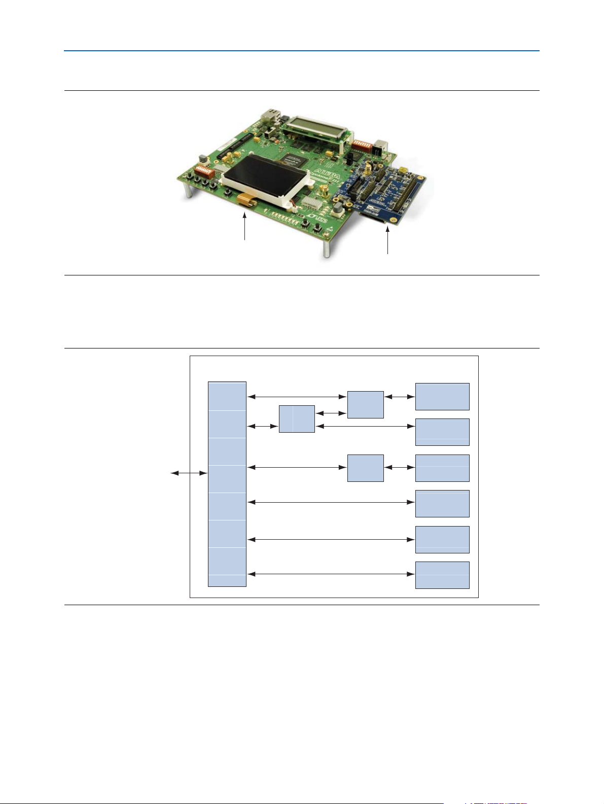
Figure 1–1 shows the THDB-SUM board used with Altera
development board. For more information about connecting the THDB-SUM board to
a host board, refer to Appendix A, Demonstration.
®
Cyclone® III FPGA
© December 2008 Altera Corporation Santa Cruz, USB, MICTOR, SD Card HSMC Reference Manual
Page 6
1–2 Chapter 1: Overview
HSMC
Connector
Santa Cruz
Connector
USB
Transceiver
SD Card
Socket
MICTOR
Connector
SMA
Connector
Level
Shifters
Level
Shifters
Bus Switch
SC
Interface
USB Interface
SD Card Interface
MICTOR Connector Interface
External Clock Input
THDB-SUM
To
HSMC Interface
Host Board
Interface
2
IC
Serial
EEPROM
2
IC
Handling the Board
Figure 1–1. THDB-SUM Board Connected to the Cyclone III FPGA Development Board
Cyclone III FPGA Development Board
THDB-SUM Board
Block Diagram
Figure 1–2 shows the functional block diagram of the THDB-SUM board.
Figure 1–2. THDB-SUM Board Block Diagram
Handling the Board
When handling the board, it is important to observe the following precaution:
c Static Discharge Precaution: Without proper anti-static handling, the board can be
damaged. Therefore, use anti-static handling precautions when touching the board.
Santa Cruz, USB, MICTOR, SD Card HSMC Reference Manual © December 2008 Altera Corporation
Page 7

Introduction
2. Board Components
This chapter introduces the important components on the THDB-SUM board and
provides their operational and connectivity details.
This chapter consists of the following sections:
■ “HSMC Connector (J1)” on page 2–4
■ “Santa Cruz Connectors (J3, J4, and J5)” on page 2–7
■ “USB On-The-Go Transceiver (U11)” on page 2–11
■ “MICTOR Connector (J2)” on page 2–13
■ “SD Card Interface (J7)” on page 2–16
■ “SMA Connector (J6)” on page 2–17
2
■ “I
C Serial EEPROM (U10)” on page 2–17
■ “Power Supply” on page 2–18
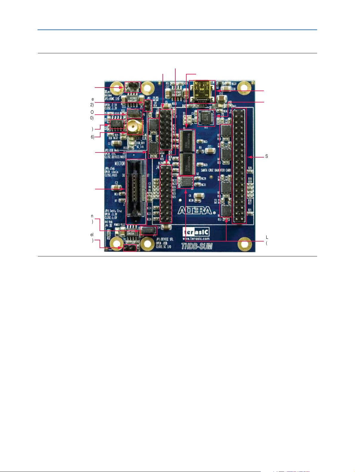
Board Overview
This section provides an overview of the THDB-SUM board, including an annotated
board image and component descriptions. Figure 2–1 shows the THDB-SUM board
and its components and locations.
© December 2008 Altera Corporation Santa Cruz, USB, MICTOR, SD Card HSMC Reference Manual
Page 8
2–2 Chapter 2: Board Components
HSMC Logic Level
Configuration Header (JP3)
USB Host/Peripheral Mode
Configuration Header (JP2)
JTAG TDI/TDO
Loopback Header (JP0)
SMA Connector (J6)
MICTOR Connector (J2)
EEPROM (U10)
Level Shifters (U7-U8)
USB/SC Function
Select Header (JP1)
SC Connector Logic Level
Configuration Header (JP4)
Mini USB AB Type
Receptacle Connector (J8)
USB On-The-Go
Transceiver (U11)
Santa Cruz Connector (J5)
Bus Switch (U1-U2)
Santa Cruz
Connector (J3)
Santa Cruz
Connector (J4)
Level Shifters
(U3-U6)
Board Overview
Figure 2–1. THDB-SUM Board and Components
Santa Cruz, USB, MICTOR, SD Card HSMC Reference Manual © December 2008 Altera Corporation
Page 9
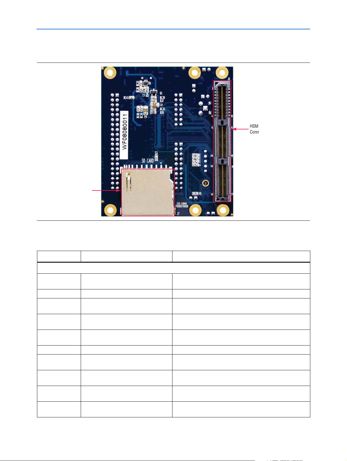
Chapter 2: Board Components 2–3
SD Card
Socket (J7)
HSMC
Connector (J1)
Board Overview
Figure 2–2 shows the back view of the THDB-SUM board.
Figure 2–2. THDB-SUM Board—Back View (HSMC Connector View)
Table 2–1 describes the components and lists their corresponding board references.
Table 2–1. THDB-SUM Board (Part 1 of 2)
Board Reference Name Description
Components and Interfaces
J1 HSMC connector Expansion connector used to interface with Altera starter and
development boards.
J2 MICTOR connector Used for logic analysis.
J3, J4, and J5 Santa Cruz connectors Expansion connectors used to connect with Santa Cruz
interface.
J6 SMA connector SMA connector that allows the provision of an external clock
input.
J7 SD card socket Used as optional external memory in both serial peripheral
interface
(SPI) and 1-bit SD mode.
J8 Mini USB AB type receptacle connector Provide USB interface to the HSMC interface host board.
JP0 JTAG TDI/TDO loopback header Used to either include or bypass daughtercard in the JTAG
chain by connecting TDI to TDO when jumper is inserted.
JP1 USB/Santa Cruz function select header Used to select between USB functionality or full Santa Cruz
header functionality.
JP2 USB Host/Peripheral mode
When closed, selects USB in host mode.
configuration header
JP3 HSMC logic level configuration header When open, selects 2.5 V HSMC source voltage.
When closed, selects 3.3 V.
© December 2008 Altera Corporation Santa Cruz, USB, MICTOR, SD Card HSMC Reference Manual
Page 10

2–4 Chapter 2: Board Components
HSMC Connector (J1)
Table 2–1. THDB-SUM Board (Part 2 of 2)
Board Reference Name Description
JP4 SC connector logic level configuration
header
When open, selects 3.3 V for Santa Cruz header I/O voltage.
When closed, selects 5.0 V.
U1–U2 Bus switches Multiplexer to switch between USB or Santa Cruz I/O based
on setting of JP2.
U3–U8 Level shifters Provides I/O level shifting based on jumper settings of JP3
and JP4.
U10 I
2
C serial EEPROM Uses one 2-Kbit EEPROM.
U11 USB On-The-Go transceiver Provide USB interface to the HSMC interface host board.
HSMC Connector (J1)
The THDB-SUM board contains an Altera standard HSMC connector (J1) to connect
to Altera FPGA starter or development board. All the other connector interfaces on
the THDB-SUM board are connected to the HSMC connector.
Figure 2–3, Figure 2–4, and Figure 2–5 show the pin-outs of the HSMC connector for
banks 1, 2, and 3, respectively.
Figure 2–3. HSMC Connector Bank 1 Pin-Outs
NC 2
NC
4
6
NC
8
NC
10
NC
12
NC
NC
14
NC
16
NC
18
NC
20
22
NC
NC
24
NC
26
NC
28
NC
30
NC
32
HSMC_SCL
HSMC_TMS
HSMC_TDI
SD_WPn
34
36
38
40
1
NC
3
NC
NC
5
NC
7
9
NC
11
NC
13
NC
15
NC
17
NC
19
NC
NC
21
23
NC
NC
25
27
NC
NC
29
NC
31
HSMC_SDA
33
35
HSMC_TCK
HSMC_TDO
37
SD_DAT1
39
Santa Cruz, USB, MICTOR, SD Card HSMC Reference Manual © December 2008 Altera Corporation
Page 11

Chapter 2: Board Components 2–5
42
44
46
48
50
52
54
56
58
60
62
64
66
68
70
72
74
76
78
80
82
84
86
88
90
92
94
96
98
100
SD_DAT3
SD_DATA2
12V
12V
12V
HSPROTO_RESET
HSPROTO_IO0
HSPROTO_IO1
HSPROTO_IO2
HSPROTO_IO3
HSPROTO_IO4
12V
HSPROTO_IO5
HSPROTO_IO6
12V
12V
12V
HSPROTO_IO7
HSPROTO_IO8
HSPROTO_IO9
HSPROTO_IO10
HSPROTO_IO11
HSPROTO_IO14
12V
EXT_CLK
CLK2
12V
HSPROTO_IO12
HSPROTO_IO13
12V
41
43
45
47
49
51
53
55
57
59
61
63
65
67
69
71
73
75
77
79
81
83
85
87
89
91
93
95
97
99
SD_DAT0
SD_CLK
VCC33
SD_CMD
HSPROTO_IO40
HSPROTO_IO29
HSPROTO_IO30
HSPROTO_IO31
HSPROTO_IO33
HSPROTO_IO32
HSPROTO_IO35
HSPROTO_IO34
HSPROTO_IO37
HSPROTO_IO36
HSPROTO_IO39
HSPROTO_IO38
HSPROTO_IO17
OSC
CLK1
HSPROTO_IO15
HSPROTO_IO16
VCC33
VCC33
VCC33
VCC33
VCC33
VCC33
VCC33
VCC33
VCC33
HSMC Connector (J1)
Figure 2–4. HSMC Connector Bank 2 Pin-Outs
© December 2008 Altera Corporation Santa Cruz, USB, MICTOR, SD Card HSMC Reference Manual
Page 12

2–6 Chapter 2: Board Components
MICTOR_D14
MICTOR_D15
12V
12V
12V
MICTOR_D16
MICTOR_D17
MICTOR_D18
MICTOR_D19
MICTOR_D20
MICTOR_D21
12V
MICTOR_D22
MICTOR_D23
12V
12V
12V
MICTOR_D24
HSPROTO_IO23
HSPROTO_IO24
HSPROTO_IO25
HSPROTO_IO26
HSPROTO_IO27
HSPROTO_CARDSEL
HSPROTO_IO28
12V
MICTOR_CLK
DEV_SEL
GND
102
104
106
108
110
112
114
116
118
120
122
124
126
128
130
132
134
136
138
140
142
144
146
148
150
152
154
156
158
160
MICTOR_D0
MICTOR_D1
MICTOR_D4
MICTOR_D5
MICTOR_D2
MICTOR_D3
MICTOR_D6
MICTOR_D13
MICTOR_D12
MICTOR_D11
MICTOR_D10
MICTOR_D9
HSPROTO_IO18
HSPROTO_IO19
HSPROTO_IO20
HSPROTO_IO21
MICTOR_D22
TR_CLK
VCC33
VCC33
VCC33
VCC33
VCC33
VCC33
VCC33
VCC33
VCC33
VCC33
101
103
105
107
109
111
113
115
117
119
121
123
125
127
129
131
133
135
137
139
141
143
145
147
149
151
153
155
157
159
R5
0
12V
MICTOR_D8
MICTOR_D7
HSMC Connector (J1)
Figure 2–5. HSMC Connector Bank 3 Pin-Outs
Santa Cruz, USB, MICTOR, SD Card HSMC Reference Manual © December 2008 Altera Corporation
Figure 2–6 shows the JTAG interface of the HSMC connector. When not using the
JTAG interface, short the header JP0 to loopback the TDI and TDO signals on the
HSMC connector.
Figure 2–6. JTAG Interface Setting of the HSMC Connector
HSMC_TDI
HSMC_TDO
HSMC_TDI HSMC_TDO
R1 0
R2 0
R3 0
R4
12
Open: JTAG Chain
Close: JTAG Pass
0
JPO
NM
NM
MICTOR_TDI
MICTOR_TDO
NM : No Mount
Page 13

Chapter 2: Board Components 2–7
DEV_SEL
USB_D[7..0]
USB_CS_n
USB_CLKOUT
Open: USB
Close: Santa Cruz
Bus
Switches
(U1, U2)
USB OTG
Transceiver
(U11)
Santa Cruz
Connectors
(J3-J5)
16
Level
Shifters
(U3-U8)
SWPROTO_RESET
SWPROTO_IO[14..0]
42
PROTO_RESET
PROTO_CARDSEL
PROTO_IO[39..0]
USB_STP
USB_DIR
USB_NXT
USB_RESET_n
14
16
HSPROTO_RESET
HSPROTO_IO[14..0]
26
HSPROTO_CARDSEL
HSPROTO_IO[39..15]
HSMC Connector
(J1)
JP1
Santa Cruz Connectors (J3, J4, and J5)
Santa Cruz Connectors (J3, J4, and J5)
The THDB-SUM board comes with Santa Cruz connectors (J3, J4, and J5) to connect to
a daughter board with Santa Cruz interface. Some of the I/O pins of Santa Cruz
connectors pass through a bus switch chip (U1 or U2) first before connecting to the
HSMC connector as shown in Figure 2–7.
Figure 2–7. I/O Distribution of the HSMC, Santa Cruz, and USB Transceiver Interface
Because of the limited number of HSMC connector I/O pins, the Santa Cruz
connectors and the USB transceiver port share the same I/O pins. Therefore, you can
only select one function at a time between a Santa Cruz connector and the USB
transceiver. To enable a function, refer to Tabl e 2–2 .
Table 2–2. Enable Function Configuration on Bus Switch Chip
JP1 Setting Enable Function
Open USB OTG Transceiver
Close Santa Cruz Connector
There are a few level shifters between the HSMC and Santa Cruz connectors as shown
in Figure 2–8. These level shifters convert the logic levels of the signals between the
HSMC and Santa Cruz connectors according to the configurations of the headers (JP3
© December 2008 Altera Corporation Santa Cruz, USB, MICTOR, SD Card HSMC Reference Manual
and JP4). With this feature, you can use different I/O standards between the HSMC
host board and the Santa Cruz interface daughter board. Table 2–3 and Table 2–4 list
the configurations of the voltage level of the HSPROTO_IO bus and the PROTO_IO
bus, respectively.
Page 14

2–8 Chapter 2: Board Components
Santa Cruz
Connectors
(J3-J5)
Level
Shifters
(U3-U8)
42
PROTO_RESET
PROTO_CARDSEL
PROTO_IO[39..0]
42
HSPROTO_RESET
HSPROTO_CARDSEL
HSPROTO_IO[39..0]
HSMC Connector
(J1)
VCCA
Open: 2.5 V
Close: 3.3 V
VCCB
Open: 3.3 V
Close: 5 V
JP3 JP4
Santa Cruz Connectors (J3, J4, and J5)
Figure 2–8. Logic Level Transform Block
Table 2–3. Logic Level Configuration on HSPROTO_IO Bus
JP3 Setting Logic Level of the HSPROTO_IO Bus
Open 2.5 V
Close 3.3 V
Table 2–4. Logic Level Configuration on PROTO_IO Bus
JP4 Setting Logic Level of the PROTO_IO Bus
Open 3.3 V
Close 2.5 V
Santa Cruz, USB, MICTOR, SD Card HSMC Reference Manual © December 2008 Altera Corporation
Page 15

Chapter 2: Board Components 2–9
PROTO_IO40
PROTO_IO30
PROTO_IO32
PROTO_IO34
PROTO_IO36
PROTO_IO38
GND
VSC
J3
PROTO_IO29
PROTO_IO31
PROTO_IO33
PROTO_IO35
PROTO_IO37
PROTO_IO39
PROTO_RESET
PROTO_IO0
PROTO_IO2
PROTO_IO4
PROTO_IO6
PROTO_IO8
PROTO_IO10
PROTO_IO12
PROTO_IO14
PROTO_IO16
PROTO_IO17
PROTO_IO18
PROTO_IO19
PROTO_IO21
PROTO_IO22
PROTO_IO24
PROTO_IO25
PROTO_IO27
PROTO_IO28
PROTO_IO1
PROTO_IO3
PROTO_IO5
PROTO_IO7
PROTO_IO9
PROTO_IO11
PROTO_IO13
PROTO_IO15
NC
GND
GND
GND
GND
GND
GND
GND
GND
GND
GND
12V
VCC33
VCC33
VCC33
VCC33
VCC33
NC
OSC
CLK1
CLK2
GND
GND
GND
GND
GND
GND
GND
PROTO_IO20
PROTO_IO23
PROTO_IO26
PROTO_CARDSEL
J5
J4
GND
3
5
7
1
9
11
13
4
6
8
2
10
12
14
3
5
7
1
9
11
13
4
6
8
2
10
12
14
15
17
19
16
18
20
3
5
7
1
9
11
13
4
6
8
2
10
12
14
15
17
19
16
18
20
21
23
25
27
29
31
33
35
37
39
22
24
26
28
30
32
34
36
38
40
Santa Cruz Connectors (J3, J4, and J5)
Figure 2–9 shows the pin-outs of the Santa Cruz connector. Detailed pin mapping
between J3, J4, and J5 to the HSMC connector is listed in Table 2–5, Table 2–6, and
Table 2–7.
f Because of the characteristic of the level shifters, the data rate of the HSPROTO_IO and
PROTO_IO bus must be under 100 Mbps.
Figure 2–9. Santa Cruz Connector Pin-Outs
Table 2–5. Santa Cruz Connector J3 Pin Assignments
Santa Cruz
Pin Number
Santa Cruz
Signal Name HSMC Pin Number HSMC Signal Name HSMC Pin Name
3 PROTO_IO40 49 HSPROTO_IO40 HSMC_TX_N0
4 PROTO_IO29 53 HSPROTO_IO29 HSMC_TX_P1
5 PROTO_IO30 55 HSPROTO_IO30 HSMC_TX_N1
6 PROTO_IO31 59 HSPROTO_IO31 HSMC_TX_P2
7 PROTO_IO32 65 HSPROTO_IO32 HSMC_TX_P3
© December 2008 Altera Corporation Santa Cruz, USB, MICTOR, SD Card HSMC Reference Manual
8 PROTO_IO33 61 HSPROTO_IO33 HSMC_TX_N2
9 PROTO_IO34 71 HSPROTO_IO34 HSMC_TX_P4
10 PROTO_IO35 67 HSPROTO_IO35 HSMC_TX_N3
11 PROTO_IO36 77 HSPROTO_IO36 HSMC_TX_P5
12 PROTO_IO37 73 HSPROTO_IO37 HSMC_TX_N4
13 PROTO_IO38 83 HSPROTO_IO38 HSMC_TX_P6
14 PROTO_IO39 79 HSPROTO_IO39 HSMC_TX_N5
Page 16

2–10 Chapter 2: Board Components
Santa Cruz Connectors (J3, J4, and J5)
Table 2–6. Santa Cruz Connector J4 Pin Assignments
Santa Cruz
Pin Number
Santa Cruz
Signal Name HSMC Pin Number HSMC Signal Name HSMC Pin Name
9 OSC 95 OSC HSMC_CLKOUT_P1
11 CLK1 97 CLK1 HSMC_CLKOUT_N1
13 CLK2 98 CLK2 HSMC_CLKIN_N1
Table 2–7. Santa Cruz Connector J5 Pin Assignments
Santa Cruz
Pin Number
Santa Cruz
Signal Name HSMC Pin Number HSMC Signal Name HSMC Pin Name
1 PROTO_RESET 48 HSPROTO_RESET HSMC_RX_P0
3 PROTO_IO0 50 HSPROTO_IO0 HSMC_RX_N0
4 PROTO_IO1 54 HSPROTO_IO1 HSMC_RX_P1
5 PROTO_IO2 56 HSPROTO_IO2 HSMC_RX_N1
6 PROTO_IO3 60 HSPROTO_IO3 HSMC_RX_P2
7 PROTO_IO4 62 HSPROTO_IO4 HSMC_RX_N2
8 PROTO_IO5 66 HSPROTO_IO5 HSMC_RX_P3
9 PROTO_IO6 68 HSPROTO_IO6 HSMC_RX_N3
10 PROTO_IO7 72 HSPROTO_IO7 HSMC_RX_P4
11 PROTO_IO8 74 HSPROTO_IO8 HSMC_RX_N4
12 PROTO_IO9 78 HSPROTO_IO9 HSMC_RX_P5
13 PROTO_IO10 80 HSPROTO_IO10 HSMC_RX_N5
14 PROTO_IO11 84 HSPROTO_IO11 HSMC_RX_P6
15 PROTO_IO12 86 HSPROTO_IO12 HSMC_RX_N6
16 PROTO_IO13 90 HSPROTO_IO13 HSMC_RX_P7
17 PROTO_IO14 92 HSPROTO_IO14 HSMC_RX_N7
18 PROTO_IO15 85 HSPROTO_IO15 HSMC_TX_N6
21 PROTO_IO16 89 HSPROTO_IO16 HSMC_TX_P7
23 PROTO_IO17 91 HSPROTO_IO17 HSMC_TX_N7
25
PROTO_IO18 143 HSPROTO_IO18 HSMC_TX_P15
27 PROTO_IO19 145 HSPROTO_IO19 HSMC_TX_N15
28 PROTO_IO20 149 HSPROTO_IO20 HSMC_TX_P16
29 PROTO_IO21 151 HSPROTO_IO21 HSMC_TX_N16
31 PROTO_IO22 155 HSPROTO_IO22 HSMC_CLKOUT_P2
32 PROTO_IO23 134 HSPROTO_IO23 HSMC_RX_N13
33 PROTO_IO24 138 HSPROTO_IO24 HSMC_RX_P14
35 PROTO_IO25 140 HSPROTO_IO25 HSMC_RX_N14
36 PROTO_IO26 144 HSPROTO_IO26 HSMC_RX_P15
37 PROTO_IO27 146 HSPROTO_IO27 HSMC_RX_N15
38 PROTO_CARDSEL 150 HSPROTO_CARDSEL HSMC_RX_P16
39 PROTO_IO28 152 HSPROTO_IO28 HSMC_RX_N16
Santa Cruz, USB, MICTOR, SD Card HSMC Reference Manual © December 2008 Altera Corporation
Page 17

Chapter 2: Board Components 2–11
USB On-The-Go Transceiver (U11)
Table 2–8 lists the Santa Cruz board reference and manufacturing information.
Table 2–8. Santa Cruz Connector Board Reference and Manufacturing Information
Manufacturing
Board Reference Description Manufacturer
J3, J4, and J5 Santa Cruz Connector Various Standard 0.1 in. dual-row headers.
J3: 14 pins. J4: 20 pins.
J5: 40 pins.
Part Number
USB On-The-Go Transceiver (U11)
The THDB-SUM board is equipped with an NXP ISP1504C USB OTG transceiver
(U11) and a Mini USB AB type receptacle connector (J8) to provide USB interface to
the HSMC interface host board. The NXP ISP1504C is a USB OTG transceiver that is
fully compliant with the Universal Serial Bus Specification Rev. 2.0, On-The-Go
Supplement to the USB 2.0 Specification Rev. 1.3 and UTMI+ Low Pin Interface (ULPI)
Specification Rev. 1.1.
As mentioned in the preceding section, the USB transceiver and Santa Cruz
connectors share the same I/O pins connected to the HSMC connector. This means
you can only select one function at a time between the USB transceiver and
Santa Cruz connectors. To select the USB transceiver function, set the JP1 header to
the open position.
f For more information about the USB transceiver, visit the NXP Semiconductors
website at www.nxp.com.
Manufacturer
Website
—
In OTG implementations, the 2-pin header JP2 is connected to the identification
(ID) pin of the USB OTG transceiver and the micro-USB receptacle. The logic level of
the ID pin on the USB OTG transceiver can be configured to logic high or low through
JP2, as shown in Figure 2–10.
As defined in the On-The-Go Supplement to the USB 2.0 Specification Rev. 1.3, the ID pin
dictates the initial role of the USB link. If the ID pin is detected as HIGH, the link must
assume the role of a peripheral. If ID pin is detected as LOW, the link must assume the
role of a host.
© December 2008 Altera Corporation Santa Cruz, USB, MICTOR, SD Card HSMC Reference Manual
Page 18

2–12 Chapter 2: Board Components
JP1 Open
Bus
Switches
(U1-U2)
USB_CLKOUT
HSPROTO_IO
HSMC Connector
(J1)
DATA[7:0]
CS
RESET
VBUS
DM
DP
ID
USB
Jack-Mini-USB-AB
JP2 Close = Host
Open = Device
USB_STP
USB_DIR
USB_NXT
DIR
STP
NXT
CLOCK
USB_D[7:0]
USB_CS_n
USB_RESET_n
NXP
ISP1504C
(U11)
XTAL1
XTAL2
XTAL1
XTAL2
X1
26 MHz
USB On-The-Go Transceiver (U11)
Figure 2–10. USB OTG Transceiver and HSMC Connector Block Diagram
Table 2–9 shows the JP2 configuration setting for the ID pin.
Table 2–9. ID Pin Configuration
JP2 Setting Host or Peripheral Role
Open Peripheral
Close Host
Table 2–10 lists the detailed pin mapping between the USB OTG transceiver and the
HSMC connector.
Table 2–10. USB OTG Transceiver (U11) Pin Assignments (Part 1 of 2)
USB Pin Number USB Signal Name HSMC Pin Number HSMC Signal Name HSMC Pin Name
1 USB_D0 48 HSPROTO_RESET HSMC_RX_P0
17 USB_RESET_n 86 HSPROTO_IO12 HSMC_RX_N6
19 USB_DIR 84 HSPROTO_IO11 HSMC_RX_P6
20 USB_STP 80 HSPROTO_IO10 HSMC_RX_N5
21 USB_NXT 78 HSPROTO_IO9 HSMC_RX_P5
23 USB_D7 74 HSPROTO_IO8 HSMC_RX_N4
24 USB_D6 72 HSPROTO_IO7 HSMC_RX_P4
25 USB_D5 68 HSPROTO_IO6 HSMC_RX_N3
26 USB_D4 66 HSPROTO_IO5 HSMC_RX_P3
27 USB_CLKOUT 62 HSPROTO_IO4 HSMC_RX_N2
28 USB_D3 60 HSPROTO_IO3 HSMC_RX_P2
29 USB_CS_n 56 HSPROTO_IO2 HSMC_RX_N1
Santa Cruz, USB, MICTOR, SD Card HSMC Reference Manual © December 2008 Altera Corporation
Page 19

Chapter 2: Board Components 2–13
VHSMC
J2
3
5
7
1
9
11
13
4
6
8
2
10
12
14
15
17
19
16
18
20
21
23
25
27
29
31
33
35
37
22
24
26
28
30
32
34
36
38
NC
NC
MICTOR_CLK
MICTOR_D24
MICTOR_D23
MICTOR_TDO
MICTOR_D22
MICTOR_TCK
MICTOR_TMS
MICTOR_D20
MICTOR_D19
MICTOR_D18
MICTOR_D17
MICTOR_D16
MICTOR_D15
MICTOR_D14
MICTOR_TDI
NC
MICTOR_D21
NC
NC
TR_CLK
MICTOR_D13
MICTOR_D12
MICTOR_D11
MICTOR_D10
MICTOR_D6
MICTOR_D5
MICTOR_D4
MICTOR_D3
MICTOR_D2
MICTOR_D1
MICTOR_D0
MICTOR_D9
MICTOR_D7
VHSMC
MICTOR_D8
MICTOR Connector (J2)
Table 2–10. USB OTG Transceiver (U11) Pin Assignments (Part 2 of 2)
USB Pin Number USB Signal Name HSMC Pin Number HSMC Signal Name HSMC Pin Name
31 USB_D2 54 HSPROTO_IO1 HSMC_RX_P1
32 USB_D1 50 HSPROTO_IO0 HSMC_RX_N0
Tabl e 2–11 lists the USB OTG transceiver board reference and manufacturing
information.
Table 2–11. USB OTG Transceiver Board Reference and Manufacturing Information
Board Reference Description Manufacturer
Manufacturing
Part Number
Manufacturer
Website
U11 USB OTG Transceiver NXP Semiconductors NXP ISP1504C www.nxp.com
MICTOR Connector (J2)
This section describes how to use the MICTOR connector (J2) on the THDB-SUM
board. The MICTOR connector can be used for logic analysis on the HSMC interface
host board by connecting an external scope or a logic analyzer to it.
Figure 2–11 shows the pin-outs of the MICTOR connector. Table 2–12 lists the detailed
pin mapping between the MICTOR connector and the HSMC connector.
Figure 2–11. MICTOR Connector Pin-Outs
Table 2–12. MICTOR Connector (J2) Pin Assignments (Part 1 of 2)
MICTOR Connector
© December 2008 Altera Corporation Santa Cruz, USB, MICTOR, SD Card HSMC Reference Manual
Pin Number
5 MICTOR_CLK 156 MICTOR_CLK HSMC_CLKIN_P2
6 TR_CLK 157 TR_CLK HSMC_CLKOUT_N2
7 MICTOR_D24 132 MICTOR_D24 HSMC_RX_P13
MICTOR Connector
Signal Name HSMC Pin Number HSMC Signal Name HSMC Pin Name
Page 20

2–14 Chapter 2: Board Components
MICTOR Connector (J2)
Table 2–12. MICTOR Connector (J2) Pin Assignments (Part 2 of 2)
MICTOR Connector
Pin Number
8 MICTOR_D13 121 MICTOR_D13 HSMC_TX_N11
9 MICTOR_D23 128 MICTOR_D23 HSMC_RX_N12
10 MICTOR_D12 125 MICTOR_D12 HSMC_TX_P12
13 MICTOR_D22 126 MICTOR_D22 HSMC_RX_P12
16 MICTOR_D11 127 MICTOR_D11 HSMC_TX_N12
18 MICTOR_D10 131 MICTOR_D10 HSMC_TX_P13
20 MICTOR_D9 133 MICTOR_D9 HSMC_TX_N13
22 MICTOR_D8 137 MICTOR_D8 HSMC_TX_P14
23 MICTOR_D21 122 MICTOR_D21 HSMC_RX_N11
24 MICTOR_D7 139 MICTOR_D7 HSMC_TX_N14
25 MICTOR_D20 120 MICTOR_D20 HSMC_RX_P11
26 MICTOR_D6 119 MICTOR_D6 HSMC_TX_P11
27 MICTOR_D19 116 MICTOR_D19 HSMC_RX_N10
28 MICTOR_D5 109 MICTOR_D5 HSMC_TX_N9
29 MICTOR_D18 114 MICTOR_D18 HSMC_RX_P10
30 MICTOR_D4 107 MICTOR_D4 HSMC_TX_P9
31 MICTOR_D17 110 MICTOR_D17 HSMC_RX_N9
32 MICTOR_D3 115 MICTOR_D3 HSMC_TX_N10
33 MICTOR_D16 108 MICTOR_D16 HSMC_RX_P9
34 MICTOR_D2 113 MICTOR_D2 HSMC_TX_P10
35 MICTOR_D15 104 MICTOR_D15 HSMC_RX_N8
36 MICTOR_D1 103 MICTOR_D1 HSMC_TX_N8
37 MICTOR_D14 102 MICTOR_D14 HSMC_RX_P8
38 MICTOR_D0 101 MICTOR_D0 HSMC_TX_P8
11 MICTOR_TDO 37 HSMC_TDO HSMC_TDO
15
17 MICTOR_TMS 36 HSMC_TMS HSMC_TMS
19 MICTOR_TDI 38 HSMC_TDI HSMC_TDI
MICTOR Connector
Signal Name HSMC Pin Number HSMC Signal Name HSMC Pin Name
MICTOR_TCK 35 HSMC_TCK HSMC_TCK
To use this interface, you must configure the JTAG interface on the HSMC interface
host board. The following procedure shows you how to use the MICTOR interface
using the Cyclone III starter board as an example:
1. Connect the THDB-SUM board to the Cyclone III starter board.
2. Remove the jumpers, JP1 and JP2, of the Cyclone III starter board to connect the
JTAG interface between the Cyclone III FPGA and the THDB-SUM board.
3. Short the TDI and TDO pins of the JTAG connector (J4), as shown in Figure 2–12.
Santa Cruz, USB, MICTOR, SD Card HSMC Reference Manual © December 2008 Altera Corporation
Page 21

Chapter 2: Board Components 2–15
Open JP1 and JP2
Short TDI and
TDO pins of J4
Close JP8 with Jumper
J4
short
THDB-SUM Board Cyclone III Starter Board
MICTOR Connector
J2
MICTOR_TDO
MICTOR_TDI
MICTOR_TDI
MICTOR_TDO
HSMC
HSMC_TDO
HSMC_TDI
HSMC_TDI
HSMC_TDO
LF_TDI
LF_TDO
JP2 JP1 OPENOPEN
TDI TDO
JTAG_TDO
LF_TDO
ADG3304
ADG3308
TDI
TDO
J4
CIII_TDO
SHORT
CLOSE
JP8
TDI
TDO
TDI
TDO
MAX 3128
Built-in
Blaster
VCC25
USB3V
Cyclone III
MICTOR Connector (J2)
Figure 2–12. Configuring Cyclone III Starter Board to Control JTAG Chain Using MICTOR Connector
4. Disable the built-in USB-Blaster by shorting JP8 on the Cyclone III starter board.
This procedure creates a closed JTAG chain as shown in Figure 2–13.
Figure 2–13. The JTAG Chain between the THDB-Sum Board and Cyclone III Starter Board
Table 2–13 lists the MICTOR connector board reference and manufacturing
information.
Table 2–13. MICTOR Connector Board Reference and Manufacturing Information
Manufacturing
Board Reference Description Manufacturer
Part Number
J2 38-pin MICTOR Connector Tyco Electronics 2-767004-2 www.tycoelectronics.com
© December 2008 Altera Corporation Santa Cruz, USB, MICTOR, SD Card HSMC Reference Manual
Manufacturer
Website
Page 22

2–16 Chapter 2: Board Components
Level
Shifters
(U9)
HSMC Connector
(J1)
9
LF_DAT2
LF_DAT3 1
2
LF_CMD
LF_CLK
5
LF_DAT0 7
LF_DAT1 8
LF_WPn 11
SD_DAT2
SD_DAT3
SD_CMD
SD_CLK
SD_DAT0
SD_DAT1
SD_WPn
DAT2
DAT3
CMD
CLK
DAT0
DAT1
WPn
SD Card Socket
(J7)
SD Card Interface (J7)
SD Card Interface (J7)
The THDB-SUM board has an SD card socket that can be accessed as an optional
external memory in both SPI and 1-bit SD mode. Figure 2–14 shows the pin-outs of
the SD card socket. Table 2–14 lists the detailed pin mapping between the SD card
socket and the HSMC connector.
Figure 2–14. SD Card Socket and HSMC Connector Block Diagram
Table 2–14. SD Card Socket (J7) Pin Assignments
SD Card Socket
Pin Number
SD Card Socket
Signal Name HSMC Pin Number HSMC Signal Name HSMC Pin Name
1 LF_DAT3 42 SD_DAT3 HSMC_D1
2 LF_CMD 47 SD_CMD HSMC_TX_P0
5 LF_CLK 43 SD_CLK HSMC_D2
7 LF_DAT0 41 SD_DAT0 HSMC_D0
8 LF_DAT1 39 SD_DAT1 HSMC_CLKOUT0
9 LF_DAT2 44 SD_DAT2 HSMC_D3
11 LF_WPn 40 SD_WPn HSMC_CLKIN0
Table 2–15 lists the SD card socket board reference and manufacturing information.
Table 2–15. SD Card Socket Board Reference and Manufacturing Information
Manufacturing
Board Reference Description Manufacturer
J7 SD Card Socket Leamax Enterprise 9301S-090001 www.leamax.com
Santa Cruz, USB, MICTOR, SD Card HSMC Reference Manual © December 2008 Altera Corporation
Part Number
Manufacturer
Website
Page 23

Chapter 2: Board Components 2–17
SMA Connector (J6)
SMA Connector (J6)
The THDB-SUM board provides an SMA connector (J6) for external clock input.
Table 2–16 shows the pin assignments of the SMA connector.
Table 2–16. SMA Connector (J6) Pin Assignments
SMA Connector
Pin Number
SMA Connector
Signal Name HSMC Pin Number HSMC Signal Name HSMC Pin Name
1 EXT_CLK 96 EXT_CLK HSMC_CLKIN_P1
Table 2–17 lists the SMA connector board reference and manufacturing information.
Table 2–17. SMA Connector Board Reference and Manufacturing Information
Board Reference Description Manufacturer
Manufacturing
Part Number
Manufacturer
Website
J6 SMA Connector Lighthorse Technologies LTI-SASF54GT www.rfconnector.com
I2C Serial EEPROM (U10)
The THDB-SUM board provides an EEPROM (U10) which can be configured by the
2
I
C interface. The size of the EEPROM is 2 Kbits and it can store board information or
user’s data. Figure 2–15 shows the pin-outs of the EEPROM. Table 2–18 lists the
detailed pin mapping between the EEPROM and the HSMC connector.
Figure 2–15. EEPROM and HSMC Connector Block Diagram
HSMC Connector
(J1)
HSMC_SCL
HSMC_SDA
SCL
SDA
Table 2–18. EEPROM (U10) Pin Assignments
EEPROM
Pin Number
EEPROM
Signal Name HSMC Pin Number HSMC Signal Name
5 HSMC_SDA 33 HSMC_SDA
6 HSMC_SCL 34 HSMC_SCL
EEPROM
(U10)
A0
A1
A2
Default Address : 0x0
R31
R32
R33
R34
R35
R36
VCC33
VCC33
VCC33
© December 2008 Altera Corporation Santa Cruz, USB, MICTOR, SD Card HSMC Reference Manual
Page 24

2–18 Chapter 2: Board Components
HSMC
Connector
(J1)
REG3
REG2
VCC50
VSC
Santa Cruz
Connector
(J3-J5)
12 V
REG1
VCCA VCCB
Level
Shifters
(U3-U8)
JP4
JP3
VCCA VCCB
Level
Shifters
(U9)
VHSMC
VCC33
VCC33
EEPROM
(U10)
MICTOR
Connector
(J2)
SD Card
Socket
(J7)
USB
(U11)
VCC50
Power Supply
Table 2–19 lists the SMA connector board reference and manufacturing information.
Table 2–19. I2C EEPROM Board Reference and Manufacturing Information
Board Reference Description Manufacturer
2
U10 2-Kbit I
C EEPROM Microchip Technology 24LC02B www.microchip.com
Power Supply
The board receives power from the 12 V and 3.3 V provided by the HSMC. These
power supplies are either used directly or regulated by an on-board regulator as
required (refer to Figure 2–16).
Figure 2–16. Power Distribution System
Manufacturing
Part Number
Manufacturer
Website
Santa Cruz, USB, MICTOR, SD Card HSMC Reference Manual © December 2008 Altera Corporation
Page 25

A. Demonstration
The following procedure shows you how to connect the THDB-SUM board to an
HSMC interface host board using a Cyclone III starter board as an example:
1. Observe the orientation of the HSMC connector when connecting the THDB-SUM
board to the Cyclone III starter board.
2. Set JP3 on the THDB-SUM board to the open position to force the voltage level to
2.5 V to match the 2.5 V I/O pins of the starter board.
3. Configure JP4 on the THDB-SUM board according to the logic level of the
Santa Cruz daughter board (refer to Table 2–4 on page 2–8).
1 There are two LVDS pairs on the HSMC connector: the HSMC_CLK_p1/n1 (forms a
closed loop through R3) and HSMC_CLKIN_p2/n2 (forms a closed loop through R4).
Using any one of the signals in an LVDS pair in single-ended mode prevents you from
using the other signal in the same pair.
© December 2008 Altera Corporation Santa Cruz, USB, MICTOR, SD Card HSMC Reference Manual
Page 26

A–2 Appendix A: Demonstration
Santa Cruz, USB, MICTOR, SD Card HSMC Reference Manual © December 2008 Altera Corporation
Page 27

Revision History
The following table displays the revision history for this reference manual.
Date Version Changes Made
December 2008 1.0 First publication
How to Contact Altera
For the most up-to-date information about Altera products, refer to the following
table.
Contact
Contact (Note 1)
Technical support Website www.altera.com/support
Technical training Website www.altera.com/training
Product literature Website www.altera.com/literature
Non-technical support (General) Email nacomp@altera.com
(Software Licensing) Email authorization@altera.com
Note to Table:
(1) You can also contact your local Altera sales office or sales representative.
Method Address
Email custrain@altera.com
Additional Information
Typographic Conventions
The following table shows the typographic conventions that this document uses.
Visual Cue Meaning
Bold Type with Initial Capital
Letters
bold type Indicates directory names, project names, disk drive names, file names, file name
Italic Type with Initial Capital Letters Indicates document titles. For example, AN 519: Stratix IV Design Guidelines.
Italic type Indicates variables. For example, n + 1.
Initial Capital Letters Indicates keyboard keys and menu names. For example, Delete key and the Options
“Subheading Title” Quotation marks indicate references to sections within a document and titles of
© December 2008 Altera Corporation Santa Cruz, USB, MICTOR, SD Card HSMC Reference Manual
Indicates command names, dialog box titles, dialog box options, and other GUI
labels. For example, Save As dialog box.
extensions, and software utility names. For example, \qdesigns directory, d: drive,
and chiptrip.gdf file.
Variable names are enclosed in angle brackets (< >). For example, <file name> and
<project name>.pof file.
menu.
Quartus II Help topics. For example, “Typographic Conventions.”
Page 28

Info–2 Additional Information
Typographic Conventions
Visual Cue Meaning
Courier type Indicates signal, port, register, bit, block, and primitive names. For example, data1,
tdi, and input. Active-low signals are denoted by suffix n. For example,
resetn.
Indicates command line commands and anything that must be typed exactly as it
appears. For example, c:\qdesigns\tutorial\chiptrip.gdf.
Also indicates sections of an actual file, such as a Report File, references to parts of
files (for example, the AHDL keyword SUBDESIGN), and logic function names (for
example, TRI).
1., 2., 3., and
a., b., c., and so on.
■ ■ Bullets indicate a list of items when the sequence of the items is not important.
Numbered steps indicate a list of items when the sequence of the items is important,
such as the steps listed in a procedure.
1 The hand points to information that requires special attention.
c
w
A caution calls attention to a condition or possible situation that can damage or
destroy the product or your work.
A warning calls attention to a condition or possible situation that can cause you
injury.
r The angled arrow instructs you to press Enter.
f The feet direct you to more information about a particular topic.
Santa Cruz, USB, MICTOR, SD Card HSMC Reference Manual © December 2008 Altera Corporation
 Loading...