

Page 1

100G Development Kit, Stratix IV GT Edition Reference
Manual
100G Development Kit, Stratix IV GT Edition
Reference Manual
101 Innovation Drive
San Jose, CA 95134
www.altera.com
MNL-01057-1.0
Subscribe
Page 2

© 2010 Altera Corporation. All rights reserved. ALTERA, ARRIA, CYCLONE, HARDCOPY, MAX, MEGACORE, NIOS, QUARTUS and STRATIX are Reg. U.S. Pat.
& Tm. Off. and/or trademarks of Altera Corporation in the U.S. and other countries. All other trademarks and service marks are the property of their respective
holders as described at www.altera.com/common/legal.html. Altera warrants performance of its semiconductor products to current specifications in accordance
with Altera’s standard warranty, but reserves the right to make changes to any products and services at any time without notice. Altera assumes no responsibility or
liability arising out of the application or use of any information, product, or service described herein except as expressly agreed to in writing by Altera. Altera
customers are advised to obtain the latest version of device specifications before relying on any published information and before placing orders for products or
services.
100G Development Kit, Stratix IV GT Edition Reference Manual September 2010 Altera Corporation
Page 3

Contents
Chapter 1. Overview
General Description . . . . . . . . . . . . . . . . . . . . . . . . . . . . . . . . . . . . . . . . . . . . . . . . . . . . . . . . . . . . . . . . . . . . . 1–1
Development Board Block Diagram . . . . . . . . . . . . . . . . . . . . . . . . . . . . . . . . . . . . . . . . . . . . . . . . . . . . . . . . 1–3
Handling the Board . . . . . . . . . . . . . . . . . . . . . . . . . . . . . . . . . . . . . . . . . . . . . . . . . . . . . . . . . . . . . . . . . . . . . . 1–3
Chapter 2. Board Components
Introduction . . . . . . . . . . . . . . . . . . . . . . . . . . . . . . . . . . . . . . . . . . . . . . . . . . . . . . . . . . . . . . . . . . . . . . . . . . . . 2–1
Board Overview . . . . . . . . . . . . . . . . . . . . . . . . . . . . . . . . . . . . . . . . . . . . . . . . . . . . . . . . . . . . . . . . . . . . . . . . . 2–2
Featured Device: Stratix IV GT Device . . . . . . . . . . . . . . . . . . . . . . . . . . . . . . . . . . . . . . . . . . . . . . . . . . . . . . 2–6
I/O Resources . . . . . . . . . . . . . . . . . . . . . . . . . . . . . . . . . . . . . . . . . . . . . . . . . . . . . . . . . . . . . . . . . . . . . . . . 2–7
MAX II CPLD EPM2210 System Controller . . . . . . . . . . . . . . . . . . . . . . . . . . . . . . . . . . . . . . . . . . . . . . . . 2–11
Configuration, Status, and Setup Elements . . . . . . . . . . . . . . . . . . . . . . . . . . . . . . . . . . . . . . . . . . . . . . . . . 2–17
Configuration . . . . . . . . . . . . . . . . . . . . . . . . . . . . . . . . . . . . . . . . . . . . . . . . . . . . . . . . . . . . . . . . . . . . . . . 2–17
Embedded USB-Blaster . . . . . . . . . . . . . . . . . . . . . . . . . . . . . . . . . . . . . . . . . . . . . . . . . . . . . . . . . . . . . 2–18
Fast Passive Parallel Download . . . . . . . . . . . . . . . . . . . . . . . . . . . . . . . . . . . . . . . . . . . . . . . . . . . . . . 2–18
JTAG Programming Header . . . . . . . . . . . . . . . . . . . . . . . . . . . . . . . . . . . . . . . . . . . . . . . . . . . . . . . . 2–19
Status Elements . . . . . . . . . . . . . . . . . . . . . . . . . . . . . . . . . . . . . . . . . . . . . . . . . . . . . . . . . . . . . . . . . . . . . . 2–20
Status LEDs . . . . . . . . . . . . . . . . . . . . . . . . . . . . . . . . . . . . . . . . . . . . . . . . . . . . . . . . . . . . . . . . . . . . . . . 2–20
Board Jumpers . . . . . . . . . . . . . . . . . . . . . . . . . . . . . . . . . . . . . . . . . . . . . . . . . . . . . . . . . . . . . . . . . . . . 2–21
Push-Button Switches . . . . . . . . . . . . . . . . . . . . . . . . . . . . . . . . . . . . . . . . . . . . . . . . . . . . . . . . . . . . . . 2–21
Setup Elements . . . . . . . . . . . . . . . . . . . . . . . . . . . . . . . . . . . . . . . . . . . . . . . . . . . . . . . . . . . . . . . . . . . . . . 2–22
Board settings DIP switch . . . . . . . . . . . . . . . . . . . . . . . . . . . . . . . . . . . . . . . . . . . . . . . . . . . . . . . . . . . 2–22
Clock Circuitry . . . . . . . . . . . . . . . . . . . . . . . . . . . . . . . . . . . . . . . . . . . . . . . . . . . . . . . . . . . . . . . . . . . . . . . . . 2–24
PLL Frequency Setup . . . . . . . . . . . . . . . . . . . . . . . . . . . . . . . . . . . . . . . . . . . . . . . . . . . . . . . . . . . . . . . . . 2–28
Single-Ended Clocks . . . . . . . . . . . . . . . . . . . . . . . . . . . . . . . . . . . . . . . . . . . . . . . . . . . . . . . . . . . . . . . . . 2–29
General User Input/Output . . . . . . . . . . . . . . . . . . . . . . . . . . . . . . . . . . . . . . . . . . . . . . . . . . . . . . . . . . . . . 2–29
User Push-Button Switches . . . . . . . . . . . . . . . . . . . . . . . . . . . . . . . . . . . . . . . . . . . . . . . . . . . . . . . . . . . . 2–29
User LEDs . . . . . . . . . . . . . . . . . . . . . . . . . . . . . . . . . . . . . . . . . . . . . . . . . . . . . . . . . . . . . . . . . . . . . . . . . . 2–30
User DIP Switches . . . . . . . . . . . . . . . . . . . . . . . . . . . . . . . . . . . . . . . . . . . . . . . . . . . . . . . . . . . . . . . . . . . 2–31
LCD . . . . . . . . . . . . . . . . . . . . . . . . . . . . . . . . . . . . . . . . . . . . . . . . . . . . . . . . . . . . . . . . . . . . . . . . . . . . . . . . 2–32
Flash Memory . . . . . . . . . . . . . . . . . . . . . . . . . . . . . . . . . . . . . . . . . . . . . . . . . . . . . . . . . . . . . . . . . . . . . . . . . 2–33
SSRAM . . . . . . . . . . . . . . . . . . . . . . . . . . . . . . . . . . . . . . . . . . . . . . . . . . . . . . . . . . . . . . . . . . . . . . . . . . . . . 2–35
Components and Interfaces . . . . . . . . . . . . . . . . . . . . . . . . . . . . . . . . . . . . . . . . . . . . . . . . . . . . . . . . . . . . . . 2–38
Transceiver Interfaces . . . . . . . . . . . . . . . . . . . . . . . . . . . . . . . . . . . . . . . . . . . . . . . . . . . . . . . . . . . . . . . . 2–38
QSFP Interface . . . . . . . . . . . . . . . . . . . . . . . . . . . . . . . . . . . . . . . . . . . . . . . . . . . . . . . . . . . . . . . . . . . . 2–39
SFP+ Interface . . . . . . . . . . . . . . . . . . . . . . . . . . . . . . . . . . . . . . . . . . . . . . . . . . . . . . . . . . . . . . . . . . . . . 2–40
CFP Interface . . . . . . . . . . . . . . . . . . . . . . . . . . . . . . . . . . . . . . . . . . . . . . . . . . . . . . . . . . . . . . . . . . . . . 2–42
Interlaken Interface . . . . . . . . . . . . . . . . . . . . . . . . . . . . . . . . . . . . . . . . . . . . . . . . . . . . . . . . . . . . . . . . 2–45
External Memory Interfaces . . . . . . . . . . . . . . . . . . . . . . . . . . . . . . . . . . . . . . . . . . . . . . . . . . . . . . . . . . . 2–48
DDR3 Interface . . . . . . . . . . . . . . . . . . . . . . . . . . . . . . . . . . . . . . . . . . . . . . . . . . . . . . . . . . . . . . . . . . . . 2–49
QDR II Interface . . . . . . . . . . . . . . . . . . . . . . . . . . . . . . . . . . . . . . . . . . . . . . . . . . . . . . . . . . . . . . . . . . . 2–56
Ethernet RGMII Interface . . . . . . . . . . . . . . . . . . . . . . . . . . . . . . . . . . . . . . . . . . . . . . . . . . . . . . . . . . . . . 2–64
Power . . . . . . . . . . . . . . . . . . . . . . . . . . . . . . . . . . . . . . . . . . . . . . . . . . . . . . . . . . . . . . . . . . . . . . . . . . . . . . . . 2–65
Power Switch . . . . . . . . . . . . . . . . . . . . . . . . . . . . . . . . . . . . . . . . . . . . . . . . . . . . . . . . . . . . . . . . . . . . . . . . 2–65
Power Distribution System . . . . . . . . . . . . . . . . . . . . . . . . . . . . . . . . . . . . . . . . . . . . . . . . . . . . . . . . . . . . 2–65
Power Measurement . . . . . . . . . . . . . . . . . . . . . . . . . . . . . . . . . . . . . . . . . . . . . . . . . . . . . . . . . . . . . . . . . 2–67
Statement of China-RoHS Compliance . . . . . . . . . . . . . . . . . . . . . . . . . . . . . . . . . . . . . . . . . . . . . . . . . . . . 2–69
September 2010 Altera Corporation 100G Development Kit, Stratix IV GT Edition Reference Manual
Page 4

iv Contents
Additional Information
Document Revision History . . . . . . . . . . . . . . . . . . . . . . . . . . . . . . . . . . . . . . . . . . . . . . . . . . . . . . . . . . . . . . 1–1
How to Contact Altera . . . . . . . . . . . . . . . . . . . . . . . . . . . . . . . . . . . . . . . . . . . . . . . . . . . . . . . . . . . . . . . . . . . 1–1
Typographic Conventions . . . . . . . . . . . . . . . . . . . . . . . . . . . . . . . . . . . . . . . . . . . . . . . . . . . . . . . . . . . . . . . . 1–1
100G Development Kit, Stratix IV GT Edition Reference Manual September 2010 Altera Corporation
Page 5

The 100G Development Kit, Stratix® IV GT Edition allows you to evaluate the
performance the Stratix IV GT transceivers and the low power benefits of the device
itself. This document provides the detailed pin-out and component reference
information required to create FPGA designs that interface with all components on
the board.
f For information about setting up the Stratix IV GT 100G development board and
using the included software, refer to the 100G Development Kit, Stratix IV GT Edition
User Guide.
General Description
1. Overview
The Stratix IV GT 100G development board provides a hardware platform for
evaluating the performance and signal integrity features of the Altera
®
Stratix IV GT
devices. The board features the following major component blocks:
■ EP4S100G5F45I1 FPGA
■ 0.95-V core
■ 1932-Pin FineLine BGA
■ EPM2210F324C3N, MAX II 256-pin CPLD
■ FPGA Configuration
■ MAX
■ 1-Gb flash storage for two configuration images (factory and user)
■ On-Board USB-Blaster
■ JTAG header for external USB-Blaster with the Quartus II Programmer
■ On-Board Memory
■ Four 2-Gb DDR3 SDRAM
■ Four 72-Mb QDR II SRAM
■ Status and Setup Elements
■ FPGA Clock Sources
®
II+Flash Fast Passive Parallel (FPP) configuration
®
(FBGA) package
TM
using the Quartus® II Programmer
■ Clock Outputs and Triggers
■ General User Input/Output
September 2010 Altera Corporation 100G Development Kit, Stratix IV GT Edition Reference Manual
Page 6

1–2 Chapter 1: Overview
General Description
■ Components and Interfaces
■ 10/100/1000 Ethernet PHY and RJ-45 jack
■ 36 transceiver channels
■ One channel for SFP+ interface
■ One channel for SFP+ with EDC interface
■ Four channels for QSFP interface
■ 10 channels for CFP interface
■ 20 channels for Interlaken interface
■ Power
■ 14-V to 20-V DC input
■ 2.5-mm barrel Jack for DC power input
■ On/Off power slide switch
■ On-board power measurement circuitry
100G Development Kit, Stratix IV GT Edition Reference Manual September 2010 Altera Corporation
Page 7
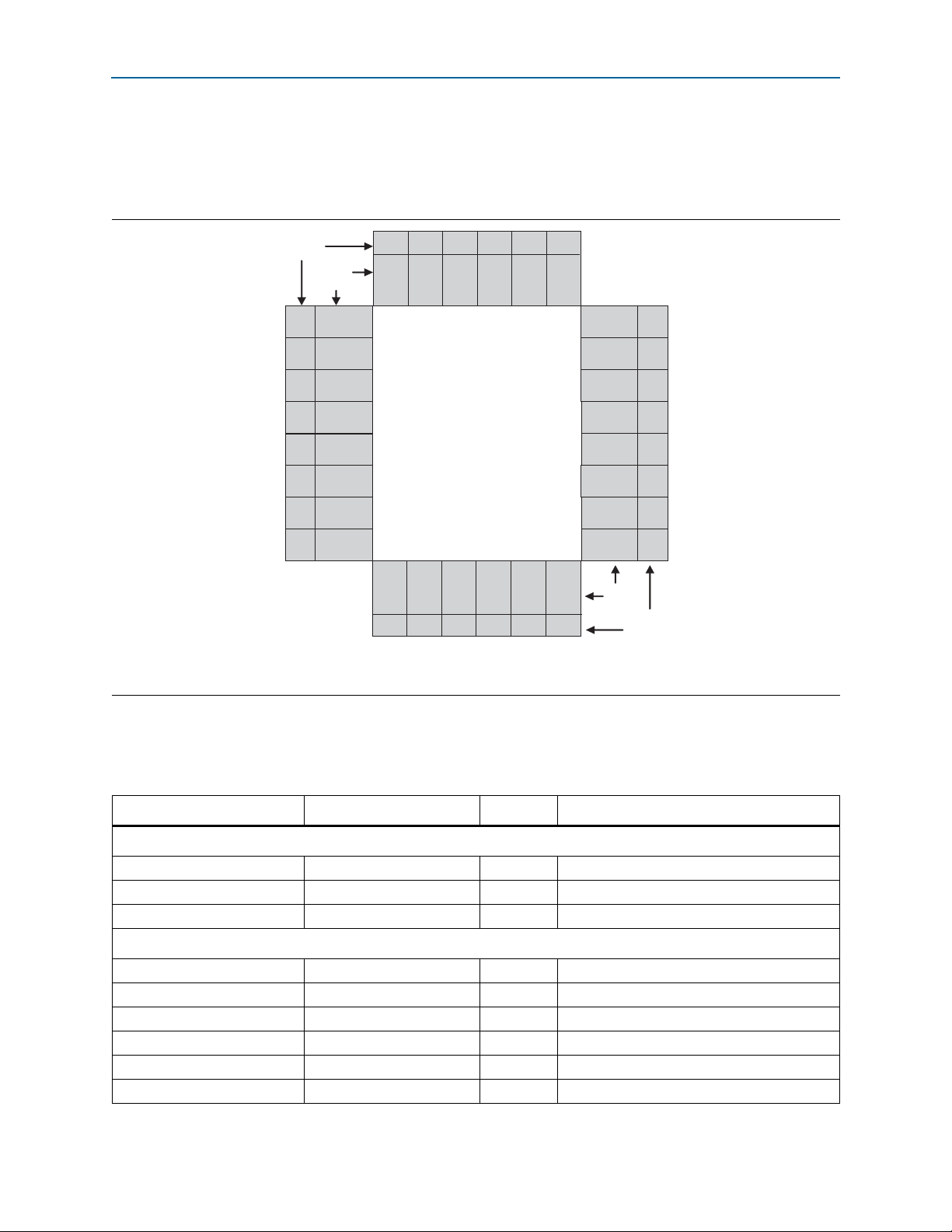
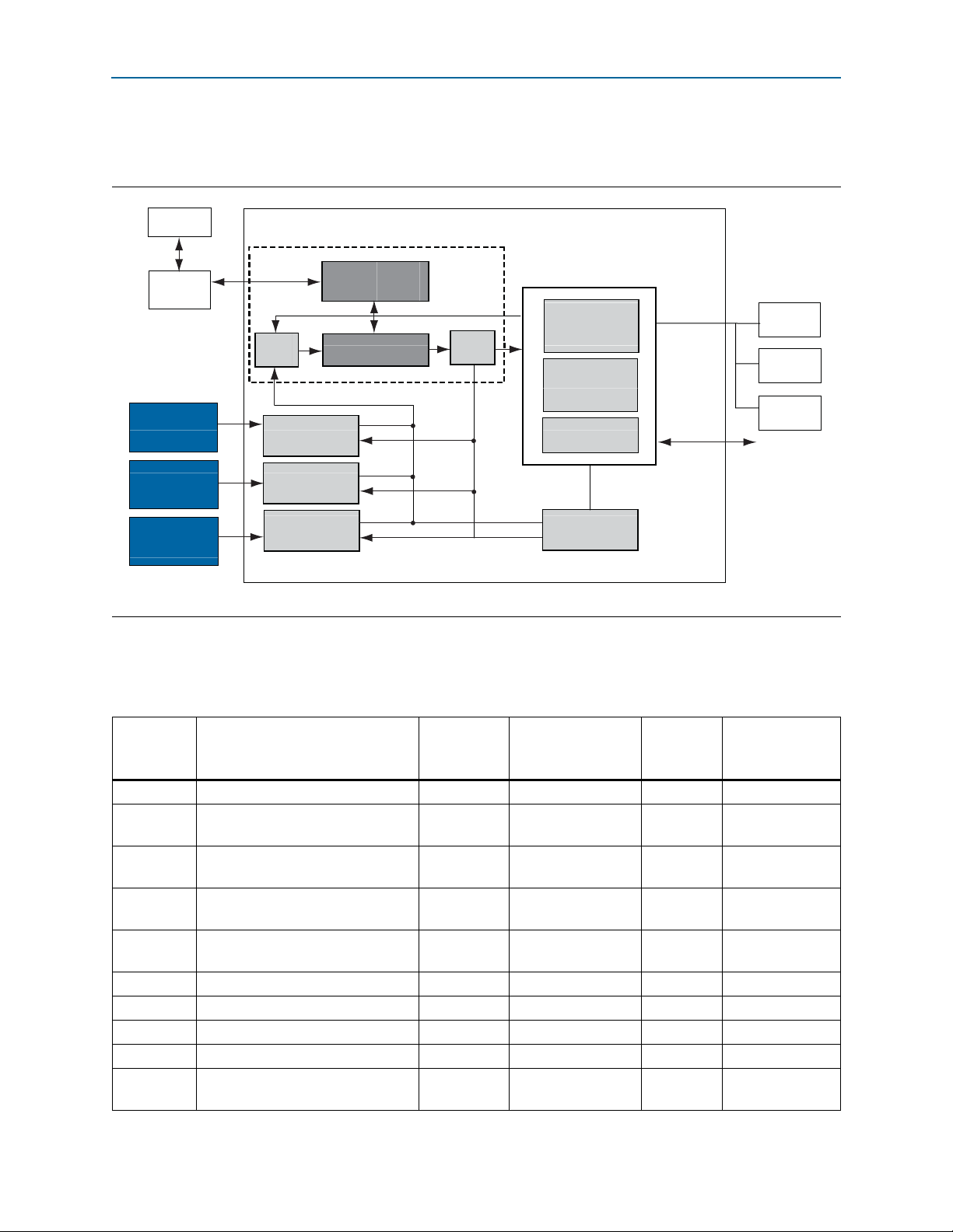
Chapter 1: Overview 1–3
EP4S100G5F1932
CPLD
(x32)
User LEDs,
Push-Buttons
USB
Blaster
10/100/1000
Ethernet
RJ45
Jack
4 MB QDR II
(x18)
64 MB
SRAM
Flash
CFP
QSFP
Clocks
& PLL
DDR3 SDRAM
(x32)
SFP+
SFP+
with EDC
Interlaken
Development Board Block Diagram
Development Board Block Diagram
Figure 1–1 shows the block diagram of the Stratix IV GT 100G development board.
Figure 1–1. Stratix IV GT 100G Development Board Block Diagram
Handling the Board
When handling the board, it is important to observe the following static discharge
precaution:
c Without proper anti-static handling, the board can be damaged. Therefore, use
anti-static handling precautions when touching the board.
The Stratix IV GT 100G development board must be stored between –40º C and
100º C. The recommended operating temperature is between 0º C and 55º C.
September 2010 Altera Corporation 100G Development Kit, Stratix IV GT Edition Reference Manual
Page 8

1–4 Chapter 1: Overview
Handling the Board
100G Development Kit, Stratix IV GT Edition Reference Manual September 2010 Altera Corporation
Page 9

Introduction
1 A complete set of schematics, a physical layout database, and GERBER files for the
f For information about powering up the board and installing the development kit
2. Board Components
This chapter introduces all the important components on the Stratix IV GT 100G
development board. Figure 2–1 illustrates major component locations and Ta bl e 2– 1
provides a brief description of all features of the board.
development board reside in the Stratix IV GT 100G development kit installation
directory.
software, refer to the 100G Development Kit, Stratix IV GT Edition User Guide.
This chapter consists of the following sections:
■ “Board Overview”
■ “Featured Device: Stratix IV GT Device” on page 2–6
■ “MAX II CPLD EPM2210 System Controller” on page 2–11
■ “Configuration, Status, and Setup Elements” on page 2–17
■ “Clock Circuitry” on page 2–24
■ “General User Input/Output” on page 2–29
■ “Flash Memory” on page 2–33
■ “SSRAM” on page 2–35
■ “Components and Interfaces” on page 2–38
■ “Power” on page 2–65
September 2010 Altera Corporation 100G Development Kit, Stratix IV GT Edition Reference Manual
Page 10
2–2 Chapter 2: Board Components
Board Overview
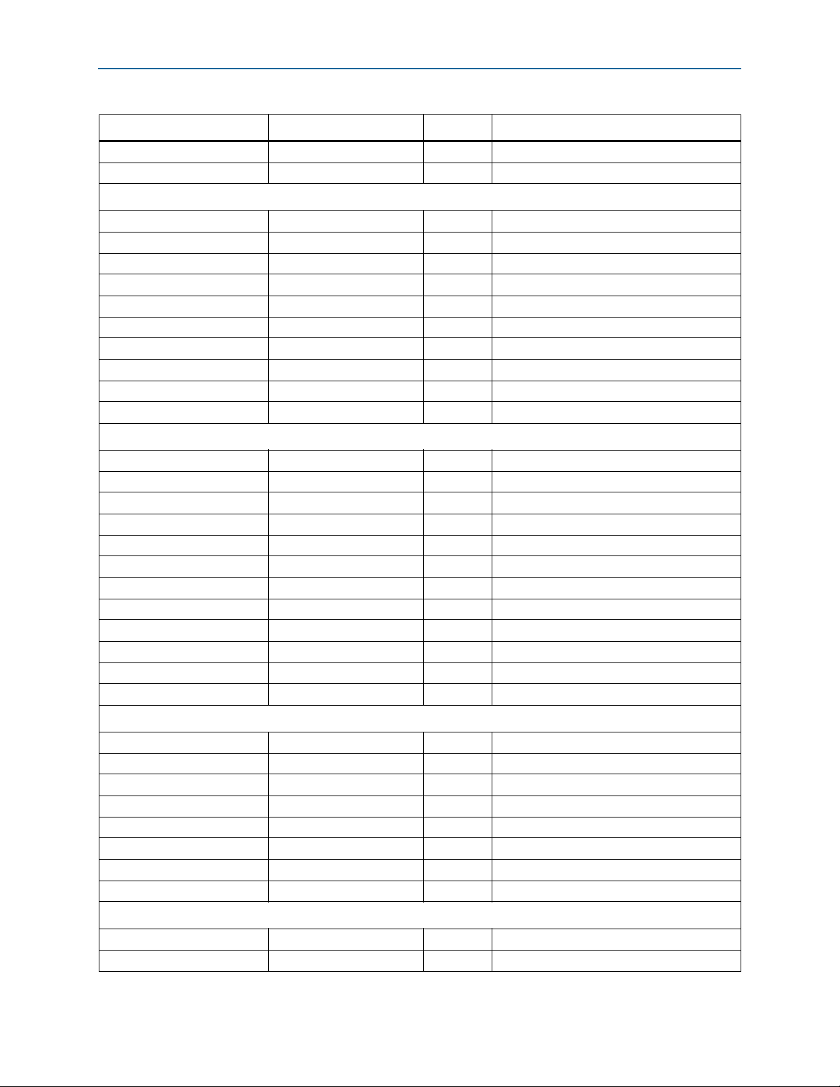
Board Overview
This section provides an overview of the Stratix IV GT 100G development board,
including an annotated board image and component descriptions. Figure 2–1
provides an overview of the board features.
Figure 2–1. Overview of the Stratix IV GT 100G Development Board Features
Power LED
(D7)
DC Power
Jack (J1)
Power
Regulators
Auxiliary
Power
Jack (J2)
Board
Settings
DIP Switch
(SW2)
Power Switch (SW1)
Interlaken Channel 10-19 (J5, J30)
DDR3 Memory
(U28-U31, U36-U39)
Stratix IV GT FPGA
(U44)
QDR II Memory
(U47-U50)
Interlaken Channel 0-9 (J39, J57)
Factory Push-Buttons
(S12)
Clock Circuitry
LCD Display (J59)
CPU Reset Push-Buttons
(S9)
User DIP Switches
(SW3, SW4)
User Push-Buttons
(S5-S8)
User LEDs (D28-D35)
MAX II CPLD (U72)
JTAG Connector (J61)
Embedded
USB-Blaster
Activity LED (D27)
Embedded
USB-Blaster (J60)
Clock Circuitry
SFP Port
B (J31)
SFP Port
A (J32)
QSFP
(J34)
CFP
(J37)
SSRAM
(U57)
Flash
Memory
(U65)
RJ45 Jack
(J49)
Ethernet
Status LEDs
(D12-D17)
Ethernet
Tab le 2 –1 describes the components and lists their corresponding board references.
Table 2–1. Stratix IV GT 100G Development Board Components (Part 1 of 5)
Board
Reference
Type Description
Featured Devices
U44 FPGA EP4S100G5F45I1 Stratix IV GT device in a 1932-Pin FBGA package.
Configuration, Status, and Setup Elements
D25, D20,
D19, D26
Configuration status LEDs LEDs to indicate the status of FPP configuration.
D7 Power LED Blue LED to indicate the board power status.
D27 USB-Blaster LED Green LED to indicate the embedded USB-Blaster activity status.
100G Development Kit, Stratix IV GT Edition Reference Manual September 2010 Altera Corporation
Page 11
Chapter 2: Board Components 2–3
Board Overview
Table 2–1. Stratix IV GT 100G Development Board Components (Part 2 of 5)
Board
Reference
D12-D17
Ethernet status LEDs Shows the Ethernet connection speed as well as transmit or receive
Type Description
activity.
D26 Factory LED Illuminates when the factory design is being loaded into the FPGA.
D36 Load LED Illuminates when the FPGA is being loaded.
D38 Error LED Illuminates when the FPGA configuration from flash fails.
D40 Configuration done LED Illuminates when the FPGA is configured.
J40 USB_DISABLE
J41 JTAG_EN
J61 JTAG programming header
J58
JTAG for embedded
USB-Blaster MAX II CPLD
Manually disables the embedded USB-Blaster when you install the
jumper. Otherwise, the embedded USB-Blaster is enabled.
Enables the MAX II CPLD EPM2210 System Controller to be in the JTAG
chain when shunted
JTAG programming header for connecting an Altera USB-Blaster dongle
to program the FPGA and MAX II CPLD devices.
JTAG for embedded USB-Blaster MAX II CPLD device programming.
S9 CPU reset push-button Press to reset the FPGA logic.
S10 PGM_SEL push-button Selects design file to load into the FPGA.
S11 Load push-button Initiates loading of the FPGA.
S12 Factory push-button Initiates loading of factory design into the FPGA.
II CPLD EPM2210 System Controller functions such as
SW2
Board settings DIP switch Controls the MAX
clock enable, power and temperature monitor, as well as voltage settings
for transceivers and SMA clock input control.
U72 MAX II CPLD (System)
U80
MAX II CPLD (Embedded
USB-Blaster)
Altera EPM2210F324C3N, MAX II 256-pin CPLD for MAX II+FPP
configuration.
Altera EPM240M100C4N, MAX II CPLD for embedded USB-Blaster
circuitry.
Clock Circuitry
J6, J12
J21, J28
J18, J25
SMA input clocks
J19, J26
J3, J14
J10, J11
J7, J13
J22, J29
J17, J24
J27, J20
SMA output clocks
J4, J15
J8, J9
J45, J52
J47, J54,
J46, J53
September 2010 Altera Corporation 100G Development Kit, Stratix IV GT Edition Reference Manual
SMA input clock for XCVR
reference clock
Reference clock for Interlaken side LVDS.
Differential clock for Interlaken side LVDS.
Reference clock for line side LVDS.
Differential clock for line side LVDS.
Single-ended clock inputs.
644.53125-MHz LVDS clock.
Reference clock SMA output for Interlaken side LVDS.
Differential clock SMA output for Interlaken side LVDS.
Reference clock SMA output for line side LVDS.
Differential clock SMA output for line side LVDS.
Single-ended clock SMA outputs.
Optical clock SMA source.
PLL output of FPGA.
XCVR reference clock for external clock source (LVPECL or LVDS).
Page 12

2–4 Chapter 2: Board Components
Board Overview
Table 2–1. Stratix IV GT 100G Development Board Components (Part 3 of 5)
Board
Reference
Type Description
U13 LVPECL to LVDS buffer 644.53125MHz LVDS clock buffer.
U15, U18, U19
U16
U20
Differential to LVDS clock
buffer
Differential divide-by-4 clock
divider
Differential to LVDS clock
buffer
Differential clock buffer (2 to 4) distributed to CMU and dedicated
differential clock inputs on the vertical banks of the FPGA.
Divide-by-4 clock circuit to provide the required clock to EDC and CFP.
Differential clock buffer (2 to 6) distributed to CMU of the FPGA and to
clock dividers for the optical clock.
U21, U22, U56 External programmable PLLs On-board programmable PLL clock source with buffers.
U14, U17 Single-ended clock buffer Single-ended clock buffer provided to each side of the FPGA.
X1
644.53125-MHz LVPECL
oscilator
644.53-MHz clock to the FPGA transceivers.
X3 50-MHz oscillator 50-MHz Nios CPU clock (CMOS).
Y1, Y2, Y3 25-MHz crystal clock 25-MHz reference clock for external PLLs.
General User Input and Output
D21–D24 User LEDs Four green LEDs for the MAX II CPLD EPM2210 System Controller.
D28–D35 FPGA LEDs Eight green LEDs for the FPGA.
J59 Character LCD Connector which interfaces to the provided 16 character × 2 line LCD
module.
S1–S4 User push-buttons
User push-buttons connected to the MAX II CPLD EPM2210 System
Controller.
S5–S8 FPGA user push-buttons User push-buttons connected to the Stratix IV GT device.
SW3
SW4
Bank of eight user DIP
switches
Bank of eight user DIP
switches
User DIP switches connected to the MAX II CPLD EPM2210 System
Controller.
User DIP switches connected to the FPGA.
Memory Devices
U28-U31,
DDR3 x16 port 4 x32 independent DDR3 memory port.
U36-U39
U47-U50 QDR II x18/x18 port 4 x18 independent (18-bit read and 18-bit write) QDR II memory port.
U65 Flash memory
Synchronous burst mode flash device which provides 1-Gb non-volatile
memory port.
Components and Interfaces
J34 QSFP_TX_P/_N[3:0]
QSFP XCVR interface (4-channels).
QSFP_RX_P/_N[3:0]
J37
CFP_TX_P/_N[9:0]
CFP_RX_P/_N[9:0]
CFP XCVR interface (10-channels).
J31 SFP+ interface SFP+ XCVR interface port B.
J32 SFP+ interface with EDC SFP+ XCVR interface port A.
J48 I/O connector General purpose expansion connector with 10 user-definable I/Os
connected to the MAX II CPLD EPM2210 System Controller.
100G Development Kit, Stratix IV GT Edition Reference Manual September 2010 Altera Corporation
Page 13
Chapter 2: Board Components 2–5
Board Overview
Table 2–1. Stratix IV GT 100G Development Board Components (Part 4 of 5)
Board
Reference
Type Description
Halo HFJ11-1G02E RJ-45 connector with integrated magnetic which
J49 RJ-45 connector
provides a 10/100/1000 Ethernet connection via a Marvell 88E1111 PHY
and the FPGA-based Altera Triple Speed Ethernet MegaCore function in
RGMII mode.
J5, J30, J39,
Interlaken interface Provides 20 transceiver channels for Interlaken.
J57
U66 10/100/1000 Ethernet PHY Marvell 88E1111 triple speed Ethernet PHY.
J60 USB Type-B connector
U79 USB PHY
Embedded USB-Blaster JTAG for programming the FPGA via a Type-B
USB cable.
FT245BL USB PHY device for configuring the FPGA using embedded
USB-Blaster.
Power
J1 DC power jack 14-V – 20-V DC power jack.
SW1
Power switch Switch to power on or off the board when power is supplied from the DC
power input jack.
U5 5-V switching regulator Supplies 5-V power to the dual switcher and other regulators for biasing.
U6 2.5-V switcher power supply
Supplies 2.5-V power to VCCIO, VCCPD, VCC_CLKIN, and VCC_PGM on
the Stratix IV GT device.
U7, U8 Dual 1.5-V switching regulator Supplies 1.5-V power to the VCCIO on the FPGA and external memory.
U9 3.3-V switcher power supply Supplies 3.3-V power.
U10 12-V switcher power supply Supplies 12-V power.
U11, U12 Dual switching regulator Supplies 0.95-V power to the FPGA core.
U27
VCCHIP (0.95V) linear
regulator
Supplies 0.95-V power to VCCHIP on the FPGA.
U26 VCCPT (1.5 V) linear regulator Supplies 1.5-V power to VCCPT on the FPGA.
U35
U42
U43
U45
U73, U74
VCC_AUX /and VCCA (2.5 V)
linear regulator
VCCL_GXB (1.2 V) linear
regulator
VCCH_GXB (1.4 V) linear
regulator
VCCT_GXB (1.2 V) linear
regulator
VCCR_GXB (1.2 V) linear
regulator (shared output)
Supplies 2.5-V power to VCC_AUX and VCCA on the FPGA.
Supplies 1.2-V power to the VCCL_GXB on the FPGA.
Supplies 1.4-V power to the VCCH_GXB on the FPGA.
Supplies 1.2-V power to the VCCT_GXB on the FPGA.
Supplies 1.2-V power to the VCCR_GXB on the FPGA.
U51, U52 ADC 8/16 Channel 24-bit Monitors the current or voltage of all FPGA power rails
U53, U54 4.25-V linear regulator Supplies 4.25-V power for current monitor circuit.
U55
VCCA_GXB (3.3 V) linear
regulator
Supplies 3.3-V power to the VCCA_GXB on the FPGA.
U60 VCCD (0.95 V) linear regulator Supplies 0.95 V power to VCCD on the FPGA.
U68 2.5-V linear regulator
Supplies 2.5-V power to the MAX II CPLD EPM2210 System Controller
for i/Os.
U23, U24, U59 3.3-V linear regulator Supplies 3.3-V power to the external PLLs.
September 2010 Altera Corporation 100G Development Kit, Stratix IV GT Edition Reference Manual
Page 14
2–6 Chapter 2: Board Components
Featured Device: Stratix IV GT Device
Table 2–1. Stratix IV GT 100G Development Board Components (Part 5 of 5)
Board
Reference
Type Description
U69 1.1-V linear regulator Supplies 1.1-V power to the 10/100/1000 Ethernet PHY.
U71 2.5-V linear regulator Supplies 2.5-V power to the USB port.
U70 LM95235 temperature sensor Monitors the FPGA temperature.
U77 3.3-V switching regulator Supplies 3.3-V power to the MAX II CPLD EPM2210 System Controller.
U33 5-V switching regulator Supplies 5-V power to the optical regulators.
U41 3.3-V linear regulator Supplies 3.3-V power to QSFP and SFP+.
U58 1.8-V linear regulator Supplies 1.8-V power to QDR II VDD.
U25 1.2-V linear regulator Supplies 1.2-V power to EDC.
U40 1.8-V linear regulator Supplies 1.8-V power to EDC.
U86 1.2-V linear regulator Supplies 1.2-V power to the translator device for CFP.
U81, U87, U88 0.75-V V
regulator Supplies 0.75 VTT/V
TT/VREF
to external memories and termination.
REF
Featured Device: Stratix IV GT Device
The Stratix IV GT 100G development board features the EP4S100G5F45I1 Stratix IV
GT FPGA device (U44) in a 1932-pin FBGA package.
f For more information about the Stratix IV GT devices, refer to the Stratix IV Device
Handbook.
Tab le 2 –2 describes the features of the Stratix IV GT EP4S100G5F45I1 device.
Table 2–2. Stratix IV GT Device EP4S100G5F45I1 Features
Features EP4S100G5F45I1
ALMs 212,480
Equivalent LEs 531,200
M9K RAM Blocks (256 × 72 bits) 1,280
M144K Blocks (2048 × 72 bits) 64
Total Memory (MLAB + M9K + M144K) Kbits 27,376
Total Transceiver Channels 48
18-bit × 18-bit Multipliers 1,024
PLLs 12
Maximum User I/O pins 781
Package Type 1932-pin FBGA
Tab le 2 –3 lists the Stratix IV GT component reference and manufacturing
information.
Table 2–3. Stratix IV GT Device Component Reference and Manufacturing Information
Board Reference Description Manufacturer
U44 Stratix IV GT F1932, Lead Free Altera
Corporation EP4S100G5F45I1 www.altera.com
Manufacturing
Part Number
Manufacturer
Website
100G Development Kit, Stratix IV GT Edition Reference Manual September 2010 Altera Corporation
Page 15
Chapter 2: Board Components 2–7
Featured Device: Stratix IV GT Device
I/O Resources
Figure 2–2 shows the bank organization and I/O count for the EP4S100G5F45I1
device in the 1932-pin FBGA package.
Figure 2–2. Stratix IV GT Device I/O Bank Diagram (Note 1)
Number
of I/Os
Bank
Name
40 Bank 1A
Bank 8B 48
Bank 8A 48
Bank 7C 32
Bank 8C 32
Bank 7A 48
Bank 7B 48
Bank 6A 38
21 Bank 1C
21 Bank 2C
13 Bank 2A
41 Bank 2B
Bank
4 (1)
GXBL2
Bank
4 (1)
GXBL1
Bank
4 (1)
GXBL0
48 Bank 3A
EP4S100G3
EP4S100G4
EP4S100G5
48 Bank 3B
32 Bank 3C
32 Bank 4C
Note to Figure 2–2:
(1) There are two additional PMA-only transceiver channels in each transceiver bank.
Tab le 2 –4 summarizes the FPGA I/O usage by function on the Stratix IV GT 100G
development board. I/O direction is with respect to the FPGA.
Table 2–4. Stratix IV GT I/O Usage Summary (Part 1 of 5)
Bank 6C 22
Bank 5C 19
Bank 5B 12
Bank 5A 42
Bank
Bank
Bank
Bank
Name
4 (1)
4 (1)
4 (1)
Number
of I/Os
GXBR2
GXBR1
GXBR0
48 Bank 4A
48 Bank 4B
Function I/O Type I/O Count Description
FPGA Transceiver Clocks
Reference clock from buffer LVDS input 12 Diff REFCLK input
Programmable clock LVDS input 2 Diff REFCLK input
SMA diff clock inputs LVDS input 6 Diff REFCLK input
FPGA Global Clocks
50-MHz clock 2.5-V CMOS input 1 Global clock
Ethernet receive clock 2.5-V CMOS input 1 Global clock
Single-ended clock from buffer 2.5-V CMOS input 4 Single-ended global clock
Differential clock from buffer LVDS input 4 Diff global clock
DDR3 clock from buffer LVDS input 8 Diff global clock
QDR II clock from buffer LVDS input 8 Diff global clock
September 2010 Altera Corporation 100G Development Kit, Stratix IV GT Edition Reference Manual
Page 16
2–8 Chapter 2: Board Components
Featured Device: Stratix IV GT Device
Table 2–4. Stratix IV GT I/O Usage Summary (Part 2 of 5)
Function I/O Type I/O Count Description
SMA diff clock input LVDS input 2 Diff global clock
SMA diff I/O or clock output — 2 Diff global I/O or clock output
Flash/SSRAM
ADDR[26:1] 2.5-V CMOS input 26 Flash address bus
DATA[31:0] 2.5-V CMOS input 32 Flash data bus
SSRAM_OEn 2.5-V CMOS output 1 SSRAM output enable
SSRAM_BWn[3:0] 2.5-V CMOS output 4 SSRAM byte write select
SSRAM_BWEn 2.5-V CMOS output 1 SSRAM byte write enable
SSRAM_ADVn 2.5-V CMOS output 1 SSRAM advance input
SSRAM_ADSCn 2.5-V CMOS output 1 SSRAM address strobe from controller
SSRAM_ADSPn 2.5-V CMOS output 1 SSRAM address strobe from processor
SSRAM_CE1n 2.5-V CMOS output 1 SSRAM chip enable
SSRAM_CLK 2.5-V CMOS output 1 SSRAM clock
DDR3 SDRAM (Four each)
DDR3_BA[2:0] 1.5-V SSTL output 12 DDR3 bank address
DDR3_DQS_P/_N[3:0] Diff 1.5-V SSTL input 32 DDR3 data strobe
DDR3_ADDR[12:0] 1.5-V SSTL output 52 DDR3 address
DDR3_DQ[31:0] 1.5-V SSTL input 128 DDR3 data
DDR3_CKE 1.5-V SSTL output 4 DDR3 clock enable
DDR3_CK_P/_N Diff 1.5-V SSTL input 8 DDR3 clock
DDR3_CSn 1.5-V SSTL output 4 DDR3 chip select
DDR3_Wen 1.5-V SSTL output 4 DDR3 write enable
DDR3_RASn 1.5-V SSTL output 4 DDR3 RAS#
DDR3_CASn 1.5-V SSTL output 4 DDR3 CAS#
DDR3_RSTn 1.5-V SSTL output 4 DDR3 reset
DDR3_ODT 1.5-V SSTL output 4 DDR3 on-die termination
QDR II SRAM (Four each)
QDR2_ADDR[20:0] 1.5-V SSTL output 84 QDR II address
QDR2_Q[17:0] 1.5-V SSTL input 72 QDR II data output
QDR2_D[17:0] 1.5-V SSTL output 72 QDR II data input
QDR2_BWSn[1:0] 1.5-V SSTL output 8 QDR II byte write select
QDR2_WPSn 1.5-V SSTL output 4 QDR II write port select
QDR2_RPSn 1.5-V SSTL output 4 QDR II read port select
QDR2_K_P/_N Diff 1.5-V SSTL output 8 QDR II clock input
QDR2_CQ_P/_N Diff 1.5-V SSTL input 8 QDR II echo clock
QSFP
QSFP_RX_P/_N[3:0] Transceiver Channel 8 QSFP receive channel
QSFP_TX_P/_N[3:0] Transceiver Channel 8 QSFP transmit channel
100G Development Kit, Stratix IV GT Edition Reference Manual September 2010 Altera Corporation
Page 17
Chapter 2: Board Components 2–9
Featured Device: Stratix IV GT Device
Table 2–4. Stratix IV GT I/O Usage Summary (Part 3 of 5)
Function I/O Type I/O Count Description
QSFP_MOD_SELn 2.5-V CMOS output 1 QSFP module select
QSFP_RSTn 2.5-V CMOS output 1 QSFP reset
QSFP_SCL 2.5-V CMOS output 1 QSFP serial 2-wire clock
QSFP_SDA 2.5-V CMOS bidirectional 1 QSFP serial 2-wire data
QSFP_INTERRUPT 2.5-V CMOS input 1 QSFP interrupt
QSFP_MOD_PRSn 2.5-V CMOS input 1 QSFP module present
QSFP_LP_MODE 2.5-V CMOS output 1 QSFP low power mode
SFP+ (Two each)
SFP_RX_P/_N Transceiver Channel 4 SFP+ receive channel
SFP_TX_P/_N Transceiver Channel 4 SFP+ transmit channel
SFP_TXDISABLE 2.5-V CMOS output 2 SFP+ transmitter disable
SFP_RATESEL[1:0] 2.5-V CMOS output 4 SFP+ rate select
SFP_MOD_ABS 2.5-V CMOS input 2 SFP+ module absent
SFP_SCL 2.5-V CMOS output 2 SFP+ serial 2-wire clock
SFP_SDA 2.5-V CMOS bidirectional 2 SFP+ serial 2-wire data
SFP_TXFAULT 2.5-V CMOS input 2 SFP+ transmitter fault
SFP_LOS 2.5-V CMOS input 2 SFP+ loss of signal
EDC
EDC_MDC 2.5-V CMOS output 1 EDC management data I/O clock
EDC_MDIO 2.5-V CMOS bidirectional 1 EDC management data I/O data
EDC_GPIO[1:0] 2.5-V CMOS input 2 EDC general purpose I/O
EDC_RESETn 2.5-V CMOS output 1 EDC reset
CFP
CFP_RX_P/_N[9:0] Transceiver Channel 20 CFP receive channel
CFP_TX_P/_N[9:0] Transceiver Channel 20 CFP transmit channel
CFP_PRG_CNTL[3:1] 2.5-V CMOS input 3 CFP programmable control I/O
CFP_PRTADR[4:0] 2.5-V CMOS output 5 CFP MDIO port address
CFP_MDC 2.5-V CMOS output 1 CFP management data I/O clock
CFP_MDIO 2.5-V CMOS bidirectional 1 CFP management data I/O data
CFP_MOD_RST 2.5-V CMOS output 1 CFP module reset
CFP_TX_DIS 2.5-V CMOS output 1 CFP transmitter disable
CFP_RX_LOS 2.5-V CMOS input 1 CFP loss of signal
CFP_PRG_ALRM[3:1] 2.5-V CMOS input 3 CFP programmable alarm
CFP_GLB_ALRM 2.5-V CMOS input 1 CFP global alarm
CFP_MOD_LOPWR 2.5-V CMOS output 1 CFP low power mode
CFP_MOD_ABS 2.5-V CMOS input 1 CFP module absent
Interlaken
INT_RX_P/_N[19:0] Transceiver channel 40 Interlaken receive channel
September 2010 Altera Corporation 100G Development Kit, Stratix IV GT Edition Reference Manual
Page 18
2–10 Chapter 2: Board Components
Featured Device: Stratix IV GT Device
Table 2–4. Stratix IV GT I/O Usage Summary (Part 4 of 5)
Function I/O Type I/O Count Description
INT_TX_P/_N[19:0] Transceiver channel 40 Interlaken transmit channel
INT_LSB_CON_TX_CLK_P/_N 1.2-V PCML 2 Interlaken reference clock input (LSB)
INT_MSB_CON_TX_CLK_P/_N 1.2-V PCML 2 Interlaken reference clock input (MSB)
INT_FLOW_CONTROL Signals 2.5-V CMOS 12 Interlaken flow control
MAX_STRATIX Bridge
FLASH_CONTROL 2.5-V CMOS output 1 FPGA flash control
MS_FLASH_BYTEN 2.5-V CMOS output 1 FPGA LCD write enable
MAX_STRATIX_RW 2.5-V CMOS output 1 FPGA Flash write enable
MAX_STRATIX_RDY 2.5-V CMOS output 1 FPGA Flash output enable
MAX_STRATIX_A[0] 2.5-V CMOS output 1 MAX output enable
MAX_STRATIX_A[1] 2.5-V CMOS output 1 MAX write enable
MAX_STRATIX_A[2] 2.5-V CMOS output 1 MAX chip select
MAX_STRATIX_A[3] 2.5-V CMOS output 1 FPGA LCD chip select
MAX_STRATIX_D[0] 2.5-V CMOS output 1 FPGA flash reset
MAX_STRATIX_D[1] 2.5-V CMOS output 1 MAX_STRATIX_D[1]
MAX_STRATIX_D[2] 2.5-V CMOS output 1 MAX_STRATIX_D[2]
MAX_STRATIX_D[3] 2.5-V CMOS output 1 MAX_STRATIX_D[3]
USB-Blaster
JTAG USB-Blaster or JTAG
header
2.5-V CMOS 5
Built-in USB-Blaster or JTAG 0.1-inch header
for debug purposes.
FPP Configuration
FPGA DCLK 2.5-V CMOS input 1 FPP Dclk
FPGA D[7:0] 2.5-V CMOS input 8 FPP data
MSEL [2:0] 2.5-V CMOS input 3 Dedicated configuration pins
NCONFIG 2.5-V CMOS input 1 Dedicated configuration pins
NSTATUS 2.5-V CMOS inout 1 Dedicated configuration pins
NCE 2.5-V CMOS input 1 Dedicated configuration pins
CONFIG_DONE 2.5-V CMOS inout 1 Dedicated configuration pins
Resets
CPU_RESETn 2.5-V CMOS input 1 Nios
®
II CPU Reset
Switches, Buttons, LEDS
User Push-buttons 2.5-V CMOS input 6 6 User Push-buttons
User DIP Switches 2.5-V CMOS input 8 8 User DIP Switches
User LEDS 2.5-V CMOS output 8 8 User LEDs (Green)
Ethernet
TXD[3:0] 2.5-V CMOS output 4 Ethernet Transmit RGMII Data Bus
TXEN 2.5-V CMOS output 1 Ethernet Transmit Enable
GTXCLK 2.5-V CMOS output 1 Ethernet Transmit Clock
100G Development Kit, Stratix IV GT Edition Reference Manual September 2010 Altera Corporation
Page 19
Chapter 2: Board Components 2–11
MAX II CPLD EPM2210 System Controller
Table 2–4. Stratix IV GT I/O Usage Summary (Part 5 of 5)
Function I/O Type I/O Count Description
RXD[3:0] 2.5-V CMOS input 4 Ethernet Receive RGMII Data Bus
RXDV 2.5-V CMOS input 1 Receive Data Valid
RXCLK 2.5-V CMOS input 1 Receive Clock
MDC 2.5-V CMOS input 1 Ethernet MII Clock
MDIO 2.5-V CMOS bidirectional 1 Ethernet MII Data
ENET_RESET 2.5-V CMOS output 1 Ethernet reset
ENET_LED_LINK1000 2.5-V CMOS output 1 Ethernet LINK1000 LED
Device I/O Total: 916
MAX II CPLD EPM2210 System Controller
The board utilizes the EPM2210 System Controller, an Altera MAX II CPLD, for the
following purposes:
■ FPGA configuration from flash memory
■ Power consumption monitoring
■ Temp er a ture m on it or in g
■ Virtual JTAG interface for PC-based power and temperature GUI
■ Control registers for clocks
■ Control registers for Remote System Update
■ Control registers for general purpose I/O and PFL.
■ Register with CPLD design revision and board information (read-only)
September 2010 Altera Corporation 100G Development Kit, Stratix IV GT Edition Reference Manual
Page 20
2–12 Chapter 2: Board Components
MAX1619
Controller
Information
Register
EMB
Blaster
MAX II Device
Si5338
Controller
SLD-HUB
PFL
FSM BUS
Power
Measure
Results
Virtual-JTAG
PC
Temperature
Measure
Results
FPGA
LTC2418
Controller
FLASH
Decoder
Encoder
GPIO
JTAG Control
SRAM
Control
Register
Fast Configuration
Downloader
Si5338
Programmable
Oscillator
MAX II CPLD EPM2210 System Controller
Figure 2–3 illustrates the MAX II CPLD EPM2210 System Controller's functionality
and external circuit connections as a block diagram.
Figure 2–3. MAX II CPLD EPM2210 System Controller Block Diagram
Tab le 2 –5 lists the I/O signals present on the MAX
Controller. The signal names and functions are relative to the MAX
II CPLD EPM2210 System
II device (U72).
Table 2–5. MAX II CPLD EPM2210 System Controller Device Pin-Out (Part 1 of 6)
EPM2210
Pin Number
Description Type
U72.U18 MAX_Stratix Bridge signal Bidirectional
U72.U16
U72.R13
U72.V15
U72.P13
U72.U14 EDC serial 2-wire clock Output
U72.N12 EDC serial 2-wire data Bidirectional
U72.T14 EDC write protect Output
U72.V12 50-MHz oscillator clock enable Output
U72.C2
Si5338 serial 2-wire clock for
memory PLL
Si5338 serial 2-wire data for
memory PLL
Si5338 serial 2-wire clock for
transceiver PLL
Si5338 serial 2-wire data for
transceiver PLL
Dual frequency control signal for
SFP+ interface clocks.
Output
Bidirectional
Output
Bidirectional
Output
Schematic Signal
MS_FLASH_BYTEN
SI5338_MEM_SCL
SI5338_MEM_SDA
SI5338_PLL_SCL
SI5338_PLL_SDA
CLK_SFP_SEL
Name
EDC_SCL
EDC_SDA
EDC_WP
CLK50_EN
Stratix IV
GT Device
Pin Name
U44.AP34 —
— U22.12, U56.12
— U22.19, U56.19
— U21.12
— U21.19
— U32.J1, U34.6
— U32.H1, U34.5
— U34.7
— X3.1
— U46.2
100G Development Kit, Stratix IV GT Edition Reference Manual September 2010 Altera Corporation
Other
Connections
Page 21
Chapter 2: Board Components 2–13
MAX II CPLD EPM2210 System Controller
Table 2–5. MAX II CPLD EPM2210 System Controller Device Pin-Out (Part 2 of 6)
EPM2210
Pin Number
Description Type
U72.J13 50-MHz clock input Input
U72.H17 FPGA initialization LED Output
U72.J1 Power monitor SPI clock Output
U72.H6 Power monitor SPI input data Output
U72.K1 Power monitor SPI output data Input
U72.M3 Loads factory image into the FPGA Output
U72.A9 FSM bus flash byte enable feature Output
U72.D9 FSM bus flash chip enable Input
Control signal from the FPGA to
U72.R14
indicate flash information being
passed through the MAX_STRATIX
Output
interface.
U72.E9 FSM bus flash output enable Output
U72.B9 FSM bus flash ready Output
U72.F9 FSM bus flash reset Output
U72.A8 FSM bus flash write enable Output
U72.B15 FPGA configuration done Input
U72.A15 Initiates new image to the FPGA Output
U72.B18 FPGA configuration data Output
U72.D14 FPGA configuration data Output
U72.A17 FPGA configuration data Output
U72.E13 FPGA configuration data Output
U72.B16 FPGA configuration data Output
U72.D13 FPGA configuration data Output
U72.C15 FPGA configuration data Output
U72.F12 FPGA configuration data Output
U72.C14 FPGA configuration clock Output
U72.E12 FPGA configuration error Input
U72.E11 FSM bus flash address Bidirectional
U72.B14 FSM bus flash address Bidirectional
U72.B13 FSM bus flash address Bidirectional
U72.A12 FSM bus flash address Bidirectional
U72.A13 FSM bus flash address Bidirectional
U72.C13 FSM bus flash address Bidirectional
U72.C12 FSM bus flash address Bidirectional
U72.D10 FSM bus flash address Bidirectional
U72.A7 FSM bus flash address Bidirectional
U72.B6 FSM bus flash address Bidirectional
U72.B7 FSM bus flash address Bidirectional
Schematic Signal
Name
CLKIN_50_MAX
CONFIGN_LED
CSENSE_SCK
CSENSE_SDI
CSENSE_SDO
FACTORY
FLASH_BYTEN
FLASH_CEN
FLASH_CONTROL
FLASH_OEN
FLASH_RDYBSYN
FLASH_RESETN
FLASH_WEN
FPGA_CONF_DONE
FPGA_CONFIGN
FPGA_DATA0
FPGA_DATA1
FPGA_DATA2
FPGA_DATA3
FPGA_DATA4
FPGA_DATA5
FPGA_DATA6
FPGA_DATA7
FPGA_DCLK
FPGA_STATUSN
FSM_A1
FSM_A2
FSM_A3
FSM_A4
FSM_A5
FSM_A6
FSM_A7
FSM_A8
FSM_A9
FSM_A10
FSM_A11
Stratix IV
GT Device
Pin Name
Other
Connections
— U67.5
— U40.2
— U61.5
— U61.4
— U62.5
— S12.2
—U65.F7
—U65.F2
U44.AR34 —
— U65.G2
— U65.A4
— U65.B5
— U65.A5
U44.AW38 TP7
U44.BA36 TP10
U44.AA33 TP13
U44.Y32 TP14
U44.P38 TP15
U44.P37 TP16
U44.U38 TP17
U44.U37 TP18
U44.R40 TP19
U44.P39 TP20
U44.AY9 TP9
U44.AY36 TP11
U44.AR6 U65.E2
U44.AL13 U65.E2, U57.R6
U44.AV6 U65.C2, U57.P6
U44.AN6 U65.A2, U57.A2
U44.AA14 U65.B2, U57.A10
U44.AN39 U65.D3, U57.B2
U44.T6 U65.C3, U57.B10
U44.P7 U65.A3, U57.P2
U44.Y14 U65.B6, U57.N6
U44.AA31 U65.A6, U57.P3
U44.AJ7 U65.C6, U57.P4
September 2010 Altera Corporation 100G Development Kit, Stratix IV GT Edition Reference Manual
Page 22
2–14 Chapter 2: Board Components
MAX II CPLD EPM2210 System Controller
Table 2–5. MAX II CPLD EPM2210 System Controller Device Pin-Out (Part 3 of 6)
EPM2210
Pin Number
Description Type
U72.C7 FSM bus flash address Bidirectional
U72.A5 FSM bus flash address Bidirectional
U72.B5 FSM bus flash address Bidirectional
U72.A4 FSM bus flash address Bidirectional
U72.A6 FSM bus flash address Bidirectional
U72.B3 FSM bus flash address Bidirectional
U72.B11 FSM bus flash address Bidirectional
U72.E8 FSM bus flash address Bidirectional
U72.C8 FSM bus flash address Bidirectional
U72.C11 FSM bus flash address Bidirectional
U72.B8 FSM bus flash address Bidirectional
U72.C4 FSM bus flash address Bidirectional
U72.B4 FSM bus flash address Bidirectional
U72.A2 FSM bus flash address Bidirectional
U72.B1 FSM bus flash address Bidirectional
U72.E10 FSM bus flash data Bidirectional
U72.A14 FSM bus flash data Bidirectional
U72.F10 FSM bus flash data Bidirectional
U72.F11 FSM bus flash data Bidirectional
U72.C5 FSM bus flash data Bidirectional
U72.D7 FSM bus flash data Bidirectional
U72.F7 FSM bus flash data Bidirectional
U72.C6 FSM bus flash data Bidirectional
U72.D11 FSM bus flash data Bidirectional
U72.B12 FSM bus flash data Bidirectional
U72.F8 FSM bus flash data Bidirectional
U72.E7 FSM bus flash data Bidirectional
U72.D8 FSM bus flash data Bidirectional
U72.D5 FSM bus flash data Bidirectional
U72.D6 FSM bus flash data Bidirectional
U72.E6 FSM bus flash data Bidirectional
FPGA initialization done LED.
U72.H13
Indicates that the FPGA is in user
Output
mode
Schematic Signal
Name
FSM_A12
FSM_A13
FSM_A14
FSM_A15
FSM_A16
FSM_A17
FSM_A18
FSM_A19
FSM_A20
FSM_A21
FSM_A22
FSM_A23
FSM_A24
FSM_A25
FSM_A26
FSM_D0
FSM_D1
FSM_D2
FSM_D3
FSM_D4
FSM_D5
FSM_D6
FSM_D7
FSM_D8
FSM_D9
FSM_D10
FSM_D11
FSM_D12
FSM_D13
FSM_D14
FSM_D15
INIT_DONE_LED
Stratix IV
GT Device
Pin Name
Other
Connections
U44.AK6 U65.D6, U57.P8
U44.Y6 U65.B7, U57.P9
U44.AA6 U65.A7, U57.P10
U44.AF6 U65.C7, U57.P11
U44.AG6 U65.D7, U57.R2
U44.AD14 U65.E7, U57.R3
U44.AE14 U65.B3, U57.R4
U44.AE6 U65.C4, U57.R8
U44.AA7 U65.D5, U57.R9
U44.AD7 U65.D4, U57.R10
U44.AG7 U65.C5, U57.R11
U44.AJ6 U65.B8, U57.B1
U44.AH6 U65.C8, U57.A1
U44.Y15 U65.F8, U57.B11
U44.AA15 U65.G8
U44.AP9 U65.E3, U57.J10
U44.AR8 U65.H3, U57.J11
U44.N6 U65.E4, U57.K10
U44.P6 U65.H4, U57.K11
U44.AV8 U65.H5, U57.L10
U44.AV7 U65.E5, U57.L11
U44.AV10 U65.H6, U57.M10
U44.AU10 U65.E6, U57.M11
U44.AW8 U65.F3, U57.D10
U44.AW9 U65.G3, U57.D11
U44.AU9 U65.F4, U57.E10
U44.AU8 U65.G4, U57.E11
U44.AR7 U65.F5, U57.F10
U44.AT8 U65.G6, U57.F11
U44.AT6 U65.F6, U57.G10
U44.AT7 U65.G7, U57G11
— D39.2
100G Development Kit, Stratix IV GT Edition Reference Manual September 2010 Altera Corporation
Page 23
Chapter 2: Board Components 2–15
MAX II CPLD EPM2210 System Controller
Table 2–5. MAX II CPLD EPM2210 System Controller Device Pin-Out (Part 4 of 6)
EPM2210
Pin Number
U72.N17
Description Type
Bidirectional
U72.M13 Bidirectional
U72.N18 Bidirectional
U72.M12 Bidirectional
U72.M16 Bidirectional
U72.L16 Bidirectional
U72.M17 Bidirectional
Spare I/Os on the MAX II device and
is designed as an I/O expander for
the FPGA. Data can be passed
through the MAX_STRATIX
interface.
U72.L15 Bidirectional
U72.M18 Bidirectional
U72.L14 Bidirectional
U72.M5
Initiates a load of the selected image
from the PFL
Input
Control signal between the MAX II
U72.R16
system controller and the MAX II
embedded USB-Blaster to indicate
Input
that configuration is done.
FPGA configuration done LED.
U72.T16
Indicates that the FPGA is loaded
Output
with the new image.
U72.T17 FPGA configuration error LED Output
U72.R15 FPGA configuration active LED Output
U72.V10 FPGA to MAX II I/O expander
U72.P10 Input
address bus
Input
U72.U11 Input
U72.R10 Input
U72.T15 FPGA to MAX II I/O expander data
U72.R12 Bidirectional
bus
Bidirectional
U72.V14 Bidirectional
U72.P12 Bidirectional
U72.T13
MAX_STRATIX interface ready
indicator
Input
Read-write signal for
MAX_STRATIX interface.
U72.V17
Control signal from the FPGA to
Input
indicate that the FPGA is accessing
the flash in BYTE mode.
U72.C17
U72.N1
Over-temperature indicator from the
temperature sense circuit
Push-button to select which image
to program into the FPGA
Input
Input
Schematic Signal
Name
LINE_SIDE0
LINE_SIDE1
LINE_SIDE2
LINE_SIDE3
LINE_SIDE4
LINE_SIDE5
LINE_SIDE6
LINE_SIDE7
LINE_SIDE8
LINE_SIDE9
LOAD
MAX_2_MAX_INITD
ONE
MAX_CONF_DONEn
MAX_ERROR
MAX_LOAD
MAX_STRATIX_A0
MAX_STRATIX_A1
MAX_STRATIX_A2
MAX_STRATIX_A3
MAX_STRATIX_D0
MAX_STRATIX_D1
MAX_STRATIX_D2
MAX_STRATIX_D3
MAX_STRATIX_RDY
MAX_STRATIX_RW
OVERTEMPn
PGM_SEL
Stratix IV
GT Device
Pin Name
Other
Connections
—J48.1
—J48.3
—J48.5
—J48.7
—J48.9
— J48.11
— J48.13
— J48.15
— J48.17
— J48.19
— S11.2
—U80.J6
— D37.2
— D38.2
— D36.2
U44.AN34 —
U44.AN33 —
U44.AT39 —
U44.AU39 —
U44.AF38 —
U44.W38 —
U44.AG31 —
U44.AK39 —
U44.AU37 —
U44.AU36 —
—
U70.4, D18.2,
D42.2
— S10.2
September 2010 Altera Corporation 100G Development Kit, Stratix IV GT Edition Reference Manual
Page 24
2–16 Chapter 2: Board Components
MAX II CPLD EPM2210 System Controller
Table 2–5. MAX II CPLD EPM2210 System Controller Device Pin-Out (Part 5 of 6)
EPM2210
Pin Number
Description Type
Single-ended clock input (limited to
U72.J6
300 MHz) in the MAX II device from
Input
clock tree A structure.
Single-ended clock input (limited to
U72.K6
300 MHz) in the MAX II device from
Input
clock tree B structure.
U72.H5
U72.J2
U72.G18
Chip select for the first current
sense ADC
Chip select for the second current
sense ADC
Status indicator for programming
the FPGA
Output
Output
Output
U72.E15 Temperature sense clock Output
U72.C16 Temperature sense data Bidirectional
U72.K4
Bidirectional
U72.L2 Bidirectional
U72.L6 Bidirectional
U72.L3 Bidirectional
U72.L5 Bidirectional
U72.M1 Bidirectional
U72.L4 Bidirectional
U72.M2 Bidirectional
USB control and data interface.
Connects to the MAX II embedded
USB-Blaster to pass USB data.
U72.K2 Output
U72.L1 Output
U72.J5 Input
U72.K3 Input
U72.K5 Output
U72.R6 User DIP switch Input
U72.U4 User DIP switch Input
U72.T6 User DIP switch Input
U72.V4 User DIP switch Input
U72.N7 User DIP switch Input
U72.T5 User DIP switch Input
U72.P7 User DIP switch Input
U72.U5 User DIP switch Input
U72.C10 User LED Output
U72.A11 User LED Output
U72.C9 User LED Output
U72.B10 User LED Output
U72.U3 User push-button Input
Schematic Signal
Name
SE_CLKA_MAX
SE_CLKB_MAX
SENSE_CE0
SENSE_CE1
STATUSN_LED
TSENSE_SMB_CLK
TSENSE_SMB_DATA
USB_MAX_D0
USB_MAX_D1
USB_MAX_D2
USB_MAX_D3
USB_MAX_D4
USB_MAX_D5
USB_MAX_D6
USB_MAX_D7
USB_MAX_PWR_ENn
USB_MAX_RDn
USB_MAX_RXFn
USB_MAX_TXEn
USB_MAX_WR
USER_DIPSW0
USER_DIPSW1
USER_DIPSW2
USER_DIPSW3
USER_DIPSW4
USER_DIPSW5
USER_DIPSW6
USER_DIPSW7
USER_LED0
USER_LED1
USER_LED2
USER_LED3
USER_PB0
Stratix IV
GT Device
Pin Name
Other
Connections
— U14.19
— U17.19
— U63.4
— U62.4
— D41.2
— U70.8
— U70.7
— U80.L11
— U80.C11
— U80.D11
— U80.E11
— U80.F11
— U80.H11
— U80.L7
— U80.L8
— U80.L3
— U80.L5
— U80.L2
— U80.L4
— U80.L6
—SW3.1
—SW3.2
—SW3.3
—SW3.4
—SW3.5
—SW3.6
—SW3.7
—SW3.8
— D24.2
— D23.2
— D22.2
— D21.2
— S4.2
100G Development Kit, Stratix IV GT Edition Reference Manual September 2010 Altera Corporation
Page 25

Chapter 2: Board Components 2–17
Configuration, Status, and Setup Elements
Table 2–5. MAX II CPLD EPM2210 System Controller Device Pin-Out (Part 6 of 6)
EPM2210
Pin Number
U72.P6 User push-button Input
U72.T4 User push-button Input
U72.R7 User push-button Input
U72.N3
U72.N5 Output
U72.N2 Output
U72.M4
U72.H1
U72.G7 Output
U72.J3 Output
U72.G6 LCD data bus Output
U72.H2 LCD data bus Output
U72.G5 LCD data bus Output
U72.H3 LCD data bus Output
U72.G4 LCD data bus Output
U72.G1 LCD data bus Output
U72.F6 LCD data bus Output
U72.G2 LCD data bus Output
Indicates which user Programmer
Object File (.pof) is loaded into the
FPGA
Indicates that factory .pof is loaded
into the FPGA
LCD control signals
Description Type
Output
Output
Output
Schematic Signal
Name
USER_PB1
USER_PB2
USER_PB3
USER1_POF
USER2_POF
USER3_POF
FACTORY_POF
LCD_CSn
LCD_D_Cn
LCD_WEn
LCD_DATA0
LCD_DATA1
LCD_DATA2
LCD_DATA3
LCD_DATA4
LCD_DATA5
LCD_DATA6
LCD_DATA7
Stratix IV
GT Device
Pin Name
— S3.2
— S2.2
— S1.2
— D19.2
— D20.2
— D25.2
— D26.2
—J59.6
—J59.4
—J59.5
—J59.7
—J59.8
—J59.9
— J59.10
— J59.11
— J59.12
— J59.13
— J59.14
Other
Connections
Tab le 2 –6 lists the MAX II CPLD EPM2210 System Controller component reference
and manufacturing information.
Table 2–6. MAX II CPLD EPM2210 System Controller Component Reference and Manufacturing Information
Board Reference Description Manufacturer
U72
IC - MAX II CPLD EPM2210
256FBGA -3 LF 1.8V VCCINT
Corporation EPM2210F256C3N www.altera.com
Altera
Manufacturing
Part Number
Manufacturer
Configuration, Status, and Setup Elements
This section describes the board’s configuration, status, and setup elements.
Configuration
The Stratix IV GT 100G development board supports three configuration methods:
■ Embedded USB-Blaster is the default method for configuring the FPGA at any
time using the Quartus II Programmer in JTAG mode with the supplied USB cable.
■ MAX II+Flash Fast Passive Parallel (FPP) download is used for configuring the
FPGA using stored images from flash memory on either power-up or pressing the
load (S11) push-button.
Website
September 2010 Altera Corporation 100G Development Kit, Stratix IV GT Edition Reference Manual
Page 26

2–18 Chapter 2: Board Components
USB Type-B
Connector
(J60)
FTDI
FT245BL
USB PHY
(U79)
USB FIFO BUS
EPM240M
MAX II
CPLD
JTAG
JTAG
JTAG Programming
Header (J61)
USB
Stratix IV GT
FPGA (U44)
■ JTAG programming header (J61) is used for configuring the FPGA using an
Configuration, Status, and Setup Elements
external USB-Blaster (not supplied) and the Quartus II Programmer.
The following sections describe each of these methods.
Embedded USB-Blaster
Figure 2–4 shows the block diagram for the embedded USB-Blaster. The USB-Blaster
is implemented using a USB Type-B connector (J60), a Future Technologies FT245BL
USB PHY device (U79), and an Altera EPM240M100C4N MAX II CPLD. This allows
the configuration of the FPGA using a USB cable directly connected between the USB
port on the board and a USB port of a PC running the Quartus II software.
The embedded USB-Blaster is automatically disabled when an external USB-Blaster is
connected to the JTAG chain at the JTAG programming header (J61).
Figure 2–4. Embedded USB-Blaster
Fast Passive Parallel Download
Figure 2–5 shows the block diagram for the MAX II+Flash FPP configuration. This
method is used for automatic configuration of the FPGA upon board power-up or
reset with the configuration programming image stored in the flash memory. The FPP
download controller is implemented within an Altera EPM240M100C4N MAX II
CPLD (U72). This CPLD controller, together with the Numonyx PC28F00AM29EWL
1-Gb CFI NOR-type flash memory (U65), performs the FPP configuration upon board
power-up or reset. The CPLD shares the flash interface with the FPGA. The
configuration program select push-button, PGM_SEL, (S10) selects between two .pof
files (factory or user) stored in the flash. The FPP controller uses the Altera Parallel
Flash Loader (PFL) megafunction to configure the FPGA by reading data from the
flash and converting it to FPP format. This data is written to the FPGA’s dedicated
configuration pins during configuration.
100G Development Kit, Stratix IV GT Edition Reference Manual September 2010 Altera Corporation
Page 27

Chapter 2: Board Components 2–19
J61
U44
Stratix IV GT
Stratix IV GT
and MAX II
JTAG
Programming
Header
Jumper to remove
MAX II CPLD from
JTAG Programming Header
TDI
TMS
TCK
LAST_TDO
S4GT_TDI
S4GT_TDO
JTAG_TMS
JTAG_TCK
JTAG_TMS
JTAG_TCK
MAX_FPP_TDI
MAX_FPP_TDO
U72
MAX II CPLD
9
5
1
3
Configuration, Status, and Setup Elements
Figure 2–5 shows the MAX II+Flash FPP configuration.
Figure 2–5. MAX II+Flash FPP Configuration
FPP Configuration
Load
Push-Button (S11)
PGM_SEL
Push-Button (S10)
MAX II CPLD
(U72)
(D26)
USER_POF LED
FACTORY_POF LED
(D38)
(D19, D20, D25)
MAX_ERROR LED
Flash
Flash
Flash
(U65)
Stratix IV GT
FPGA
(U44)
After a power-up or load event, the MAX II CPLD (U72) automatically configures the
FPGA in FPP mode with either the pre-installed factory .pof file or a user .pof file.
Additionally, three green configuration status LEDs (D39, D40, D41) indicate the
status of the FPP configuration.
After configuration completes, you can determine which .pof image is loaded into the
FPGA by observing the
USER3_POF
LEDs (D19, D20, D25).
JTAG Programming Header
Figure 2–6 shows the schematic connections for the dedicated JTAG programming
header (J61). This header provides another method for configuring the FPGA (U44)
using an Altera USB-Blaster with the Quartus II Programmer running on a PC. The
MAX II JTAG configuration jumper allows the MAX II CPLD device to be removed
from the JTAG chain so that the FPGA is the only device on the JTAG chain.
Figure 2–6. JTAG Programming Header
FACTORY_POF
LED (D26) or the
USER1_POF, USER2_POF
,
September 2010 Altera Corporation 100G Development Kit, Stratix IV GT Edition Reference Manual
Page 28

2–20 Chapter 2: Board Components
Configuration, Status, and Setup Elements
Status Elements
The development board includes board-specific status LEDs and switches for
enabling and configuring various features on the board, as well as a 16 character × 2
line LCD for displaying board power and temperature measurements. This section
describes these status and setup elements.
Status LEDs
Surface mount LEDs indicate the various status of the board. A logic 0 is driven on the
I/O port to turn the LED on while a logic 1 is driven to turn the LED off.
Tab le 2 –7 lists the LED board references, names, and functional descriptions.
Table 2–7. Status LEDs
Board
Reference
D7 Power
D12 DUPLEX
D13 1000
D14 100
D15 10
D16 TX
D17 RX
D19,
D20,
D25
D26 Factory
D27 USB
LED Name LED Description
Blue LED. Illuminates when the board
power switch (SW1) is on. Driven by the
3.3-V regulator.
Green LED. Illuminates to indicate Ethernet
full duplex status. Driven by the Marvell
88E1111 PHY.
Green LED. Illuminates to indicate Ethernet
linked at 1000-Mbps connection speed.
Driven by the Marvell 88E1111 PHY.
Green LED. Illuminates to indicate Ethernet
linked at 100-Mbps connection speed.
Driven by the Marvell 88E1111 PHY.
Green LED. Illuminates to indicate Ethernet
linked at 10-Mbps connection speed.
Driven by the Marvell 88E1111 PHY.
Green LED. Blinks to indicate Ethernet PHY
transmit activity. Driven by the Marvell
88E1111 PHY.
Green LED. Blinks to indicate Ethernet PHY
receive activity. Driven by the Marvell
88E1111 PHY.
Green LED. Illuminates when the user .pof
User
image is successfully programmed into the
FPGA.
Green LED. Illuminates when the factory
.pof image is successfully programmed
into the FPGA.
Green LED. Blinks to indicate the
embedded USB-Blaster activity.
Schematic
Signal Name
———
ENET_LED_DUPLEX
ENET_LED_LINK1000
ENET_LED_LINK100
ENET_LED_LINK10
ENET_LED_TX
ENET_LED_RX
USER1_POF
USER2_POF
USER3_POF
FACTORY_POF
USB_LED
I/O
Standard
2.5-V
CMOS
3.3-V
CMOS
Other
Connections
U66.60,
U66.70
U66.73,
U44.AU35
U66.74,
U44.AU35
U66.64,
U66.76
U66.68,
U66.61
U66.69,
U66.65
U72.N3
U72.N5
U72.N2
U72.M4
U80.L1
100G Development Kit, Stratix IV GT Edition Reference Manual September 2010 Altera Corporation
Page 29

Chapter 2: Board Components 2–21
Configuration, Status, and Setup Elements
Table 2–7. Status LEDs
Board
Reference
LED Name LED Description
Schematic
Signal Name
I/O
Standard
Other
Connections
Green LED. Illuminates when the MAX II
D36 Loading
CPLD is actively configuring the FPGA.
Driven by the MAX II System Controller
MAX_LOAD
U72.R15
CPLD.
D37 MAX_CONF
Green LED. Illuminates when the FPGA is
successfully configured. Driven by the
FPGA.
MAX_CONF_DONE
2.5-V
CMOS
U72.H17
Red LED. Illuminates when the MAX II
D38 Error
CPLD EPM2210 System Controller fails to
configure the FPGA. Driven by the MAX II
MAX_ERROR
U72.T17
CPLD EPM2210 System Controller.
Tab le 2 –8 lists the board-specific LEDs component references and manufacturing
information.
Table 2–8. Status LEDs Component References and Manufacturing Information
Board Reference
D12–D17, D19, D20, D25,
D26, D27, D36, D37
Device
Description
Manufacturer
Manufacturer
Part Number
Green LEDs Lumex Inc. SML-LX1206GC-TR www.lumex.com
Manufacturer
Website
D38 Red LED Lumex Inc. SML-LX1206IC-TR www.lumex.com
D7 Blue LED Lumex Inc. SML-LX1206USBC-TR www.lumex.com
Board Jumpers
Tab le 2 –9 lists the board jumper references, names, and functional descriptions.
Table 2–9. Board Jumpers
Board
Reference Jumper Name Description
J41
MAXII BYPASS
■ Jumper installed – the MAX II CPLD device (U72) is included in the JTAG
programming chain.
■ Jumper removed – the MAX II CPLD device (U72) is removed from the JTAG
programming chain.
J40
USB_DISABLEn
■ Jumper installed – the embedded USB-Blaster is disabled.
■ Jumper removed (default) – the embedded USB-Blaster is enabled.
Push-Button Switches
Board reference S9 is the CPU reset push-button switch, CPU_RESETn, which is an
input to the Stratix IV GT device. The CPU_RESETn is intended to be the master reset
signal for the FPGA design loaded into the Stratix IV GT device. The CPU_RESETn
signal must be enabled within the Quartus II software for this reset function to work.
Otherwise, the CPU_RESETn acts as a regular I/O pin. When enabled in the Quartus
II software, and then set to logic 1 on the board, this switch resets every register
within the FPGA.
September 2010 Altera Corporation 100G Development Kit, Stratix IV GT Edition Reference Manual
Page 30

2–22 Chapter 2: Board Components
Configuration, Status, and Setup Elements
Board references S10-S12 are push-button switches for MAX II+Flash FPP
configuration. Use the
PGM_SEL
(S10) push-button to select the configuration
programming image stored in the flash memory.
Tab le 2 –1 0 lists the push-button switches references, names, and functional
descriptions.
Table 2–10. Push-Button Switches
Board Reference Push-Button Switch Name Description
S9
S10
S11
S12
CPU_RESETn
PGM_SEL
LOAD
FACTORY
Reset signal for the FPGA.
Selects between two .pof files (factory or user) stored in the flash.
Initiates loading of the FPGA.
Initiates loading of factory design into the FPGA.
Tab le 2 –11 lists the push-button switches component references and the
manufacturing information.
Table 2–11. Push-Button Switches Component References and Manufacturing Information
Board Reference Device Description Manufacturer
S9–S12 Push-Button switches Panasonic Corporation EVQPAC07K www.panasonic.com
Manufacturer
Part Number
Manufacturer
Setup Elements
The development board includes the board settings DIP switch as part of the setup
elements.
Board settings DIP switch
The development board includes a board settings DIP switch which controls various
features specific to the board and the MAX
design.
Tab le 2 –1 2 lists the board settings DIP switch controls and descriptions.
Table 2–12. Board Settings DIP Switch Controls
Board
Reference
SW2.1
SW2.2
SW2.3
SW2.4
Disables the embedded USB-Blaster. USB_DISABLEn
Selects SMA or PLL for the
differential clock that goes to the
global clock inputs of clock A tree
structure.
Selects SMA or PLL that goes to the
transceivers of clock A tree structure.
Selects SMA or PLL for the
single-ended clock that goes to the
global clock inputs of clock A tree
structure.
Description
Schematic Signal
Name
DIFFCLKA_SEL
REFCLKA_SEL
SE_CLKA_SEL
II CPLD EPM2210 System Controller logic
I/O
Standard
2.5-V
Other
Connections
U80.H2
U19.3
U15.3
U14.3
Website
Settings (1)
1: Enabled
0: Disabled
1: PLL input
0: SMA input
1: PLL input
0: SMA input
1: SMA input
0: PLL input
100G Development Kit, Stratix IV GT Edition Reference Manual September 2010 Altera Corporation
Page 31

Chapter 2: Board Components 2–23
Configuration, Status, and Setup Elements
Table 2–12. Board Settings DIP Switch Controls
Board
Reference
SW2.5
Description
Selects SMA or PLL for the
differential clock that goes to the
global clock inputs of clock B tree
Schematic Signal
Name
DIFFCLKB_SEL
I/O
Standard
Other
Connections
U18.3
structure.
SW2.6
SW2.7
Selects SMA or PLL that goes to the
transceivers of clock B tree structure.
Selects SMA or PLL for the
single-ended clock that goes to the
global clock inputs of clock B tree
REFCLKB_SEL
SE_CLKB_SEL
U20.28
2.5-V
U17.3
structure.
SW2.8
Note to Table 2–12:
(1) When the switch is in the OFF position, a logic 1 is selected while in the ON position, a logic 0 is selected.
Enables the 644.53125-MHz clock. CLK644_EN
X1.1
Tab le 2 –1 3 lists the board settings DIP switch component reference and
manufacturing information.
Table 2–13. Board Settings DIP Switch Component References and Manufacturing Information
Board
Reference
Device Description Manufacturer
Manufacturer
Part Number
Manufacturer Website
SW2 DIP switch Grayhill Corporation 76SB08ST www.grayhill.com
Settings (1)
1: PLL input
0: SMA input
1: SMA input
0: PLL input
1: SMA input
0: PLL input
1: Enabled
0: Disabled
September 2010 Altera Corporation 100G Development Kit, Stratix IV GT Edition Reference Manual
Page 32

2–24 Chapter 2: Board Components
Optical Clock B Out
(For Divide-by-4 Circuit)
Reference Clock A Out
(For Interlaken Side)
Reference Clock A In
(For Interlaken Side)
Buffered Differential
Clock A Out
Differential
Clock A In
Buffered Differential
Clock B Out
Differential
Clock B In
Reference Clock B
In (For Line Side)
Reference Clock B
Out (For Line Side)
644-MHz Clock Out
Single-Ended Clock In/Out B
Single-Ended Clock In/Out A
Clock Circuitry
Clock Circuitry
This section describes the clock tree structure for the Stratix IV GT 100G Development
board.
Figure 2–7 shows the Stratix IV GT 100G development board clock circuitry.
Figure 2–7. Stratix IV GT 100G Development Board Clock Circuitry
The clock tree structure for the board is distributed into two—clock A and clock B.
Clock A is for the Interlaken interface and clock B is for the line side interface. The
PLL/buffer device (Si5338) sources both clock trees which is then distributed to the
reference clock buffer (
DIFF_CLK
buffer fans out the clock to dedicated clock inputs on the vertical I/Os of the
FPGA. A third differential clock from the
clock buffer (
SE_CLK
REF_CLK
). The
) and to the differential clock buffer (
SE_CLK
DIFF_CLK
buffer distributes the clock to every side of the
buffer goes to the single-ended
DIFF_CLK
). The
FPGA.
The
REF_CLK
and 2 on the right side of the FPGA (or left side of the die). The
for clock A tree structure distributes its input clock to transceiver block 1
REF_CLK
for clock B
tree structure distributes the clock to all four transceiver blocks on the left side of the
FPGA (or right side of the die).
100G Development Kit, Stratix IV GT Edition Reference Manual September 2010 Altera Corporation
Page 33

Chapter 2: Board Components 2–25
Reference
Clock
PLL
LVPECL
to
LVDS
Differential
Clock
Single-Ended
Clock
25 MHz
LVCMOS
644 MHz
Reference
Clock
PLL
Differential
Clock
LVPECL
25 MHz
(Same
oscillator as
in Clock A)
Divide-by-4
Circuit
LVDS
Clock A
Clock B
LVDS
LVDS
LVDS
LVDS
LVDS
LVDS
LVDS
LVDS
LVDS
LVDS
Interlaken Side
Line Side
LVPECL
LVPECL
Single-Ended
Clock
LVCMOS
XFP
CFP
Si5338
(Part A)
Si5338
(Part B)
Clock Circuitry
Figure 2–7 shows the Stratix IV GT 100G development board clock tree structure.
Figure 2–8. Stratix IV GT 100G Development Board Clock Tree Structure
The clock distribution path is done using the board settings DIP switch (SW2). This
DIP switch is located near the differential clock buffer B. Refer to Ta bl e 2– 12 on the
switch settings and descriptions. The
USB_DISABLEn
DIP switch is connected to the
MAX II device and controls the traffic that passes through the USB connector.
September 2010 Altera Corporation 100G Development Kit, Stratix IV GT Edition Reference Manual
Page 34

2–26 Chapter 2: Board Components
Clock Circuitry
Two PLL/buffer devices (Si5338) drive the DDR3 and QDR II interfaces clocks
directly to the FPGA clock pins (as shown in the Figure 2–9).
Figure 2–9. Memory Clocks
DDR3 Clocks
PLL
Stratix IV GT
25 MHz
Si5338
QDR II Clocks
PLL
Stratix IV GT
25 MHz
Si5338
Tab le 2 –1 4 lists the clock signal names, board references, and functional descriptions.
Table 2–14. Spread Spectrum Configuration DIP Switch Pin-Out (SW2) (Part 1 of 3)
Stratix IV
Board
Reference Description
U21.9 XCVR PLL clock for differential clock
Schematic
Signal Name
BUFFA1_DIFF_CLK_P
I/O
Standard
GT Device
Pin Name
— U19.6
buffer A
U21.10 XCVR PLL clock for differential clock
BUFFA1_DIFF_CLK_N — U19.7
buffer A
U21.13 XCVR PLL clock for reference clock
BUFFA2_REF_CLK_P — U15.6
buffer A
U21.14 XCVR PLL clock for reference clock
BUFFA2_REF_CLK_N — U15.7
buffer A
U21.17 XCVR PLL clock for differential clock
BUFFB1_DIFF_CLK_P — U18.6
buffer B
U21.18 XCVR PLL clock for differential clock
buffer B
U21.21 XCVR PLL clock for reference clock
BUFFB1_DIFF_CLK_N — U18.7
BUFFB2_REF_CLK_P — U20.16
LVDS
buffer B
U21.22 XCVR PLL clock for reference clock
BUFFB2_REF_CLK_N — U20.15
buffer B
U22.9 DDR3 PLL clock A DDR3_CLKA_P J21 —
U22.10 DDR3 PLL clock A DDR3_CLKA_N J20 —
U22.13 DDR3 PLL clock B DDR3_CLKB_P N24 —
U22.14 DDR3 PLL clock B DDR3_CLKB_N N23 —
U22.17 DDR3 PLL clock C DDR3_CLKC_P M22 —
U22.18 DDR3 PLL clock C DDR3_CLKC_N M21 —
U22.21 DDR3 PLL clock D DDR3_CLKD_P R23 —
Other
Connections
100G Development Kit, Stratix IV GT Edition Reference Manual September 2010 Altera Corporation
Page 35

Chapter 2: Board Components 2–27
Clock Circuitry
Table 2–14. Spread Spectrum Configuration DIP Switch Pin-Out (SW2) (Part 2 of 3)
Stratix IV
Board
Reference Description
U22.22 DDR3 PLL clock D DDR3_CLKD_N
Schematic
Signal Name
I/O
Standard
GT Device
Pin Name
P23 —
Other
Connections
U56.9 QDR II PLL clock A QDR2_CLKA_P AK21 —
U56.10 QDR II PLL clock A QDR2_CLKA_N AL22 —
U56.13 QDR II PLL clock B QDR2_CLKB_P AJ22 —
U56.14 QDR II PLL clock B QDR2_CLKB_N AK22 —
U56.17 QDR II PLL clock C QDR2_CLKC_P AJ24 —
U56.18 QDR II PLL clock C QDR2_CLKC_N AK23 —
U56.21 QDR II PLL clock D QDR2_CLKD_P AK24 —
U56.22 QDR II PLL clock D QDR2_CLKD_N AL25 —
U18.4 SMA input for differential clock buffer B SMA_DIFF_CLKIN_P1 —J19.1
U18.5 SMA input for differential clock buffer B SMA_DIFF_CLKIN_N1 —J26.1
U18.15 Differential clock buffer B to FPGA
BUFFB3_SE_CLK_P —J17.5
fabric
U18.14 Differential clock buffer B to FPGA
BUFFB3_SE_CLK_N —J17.6
LVDS
fabric
U18.12 Differential clock buffer B to SMA BUFFB_CLK_P —J20.1
U18.11 Differential clock buffer B to SMA BUFFB_CLK_N —J27.1
U20.6 SMA input for reference clock buffer B REFCLK_OSC_P —J18.1
U20.7 SMA input for reference clock buffer B REFCLK_OSC_N —J25.1
U20.3 Reference clock buffer B to transceivers REFCLK_QL0_P BB2 —
U20.4 REFCLK_QL0_N BB1 —
U20.18 REFCLK_QL1_P AK2 —
U20.19 REFCLK_QL1_N AK1 —
U20.12 REFCLK_QL2_P V2 —
U20.13 REFCLK_QL2_N V1 —
U20.10 REFCLK_QL3_P F2 —
U20.11 REFCLK_QL3_N F1 —
U17.4 SMA input for single-ended clock buffer
SE_CLKINB_SMA
—J14.1
B
U17.23 Single-ended clock buffer B SE_CLKB_L V7 —
U17.21 SE_CLKB_R AD39 —
2.5-V
CMOS
U17.19 SE_CLKB_MAX — U72.K6
U17.13 SE_CLKOUTB_SMA —J15.1
September 2010 Altera Corporation 100G Development Kit, Stratix IV GT Edition Reference Manual
Page 36

2–28 Chapter 2: Board Components
Clock Circuitry
Table 2–14. Spread Spectrum Configuration DIP Switch Pin-Out (SW2) (Part 3 of 3)
Stratix IV
Board
Reference Description
U19.4 SMA input for differential clock buffer A SMA_DIFF_CLKIN_P0
Schematic
Signal Name
I/O
Standard
GT Device
Pin Name
Other
Connections
—J21.1
U19.5 SMA input for differential clock buffer A SMA_DIFF_CLKIN_N0 —J28.1
U19.20 Differential clock buffer A to FPGA
U19.19 DIFFCLK_B5_N AC6 —
fabric
DIFFCLK_B5_P AD6 —
U19.17 DIFFCLK_B6_P W6 —
U19.16 DIFFCLK_B6_N V6 —
U19.15 BUFFA3_SE_CLK_P — U14.5
U19.14 BUFFA3_SE_CLK_N — U14.6
U19.12 Differential buffer A to SMA BUFFA_DIFF_CLK_P —J22.1
U19.11 Differential buffer A to SMA BUFFA_DIFF_CLK_N —J29.1
U15.4 SMA input for reference clock buffer A SMA_REF_CLKIN_P — J6.1
U15.5 SMA input for reference clock buffer A SMA_REF_CLKIN_N —J12.1
U15.20 Reference clock buffer A to the
U15.19 REFCLK_QR1_N AK44 —
transceivers
REFCLK_QR1_P AK43 —
LVDS
U15.17 REFCLK_QR2_P V43 —
U15.16 REFCLK_QR2_N V44 —
U15.15 BUFFA_REF_CLK_P — J7.1
U15.14 BUFFA_REF_CLK_N —J13.1
J47.1 Reference clock SMA input to FPGA
J54.1 REFCLK_QR0_N BD41 —
fabric
REFCLK_QR0_P BC41 —
J46.1 REFCLK_QR3_P F43 —
J53.1 REFCLK_QR3_N F44 —
U14.4 SMA input for single-ended clock buffer
SE_CLKINA_SMA
— J3.1
A
U14.23 Single-ended clock buffer A SE_CLKA_L AB6 —
U14.21 SE_CLKA_R V39 —
2.5-V
CMOS
U14.19 SE_CLKA_MAX —U72.J6
U14.13 SE_CLKOUTA_SMA — J4.1
U13.1 644-MHz reference clock buffer CLK_644_P
U13.2 644-MHz reference clock buffer CLK_644_N —J11.1
U67.2 50-MHz single-ended clock buffer to
CLKIN_50_FPGA
FPGA fabric
U67.5 50-MHz single-ended clock to MAX CLKIN_50_MAX — U72.J13
LVDS
2.5-V
CMOS
—J10.1
AC39 —
PLL Frequency Setup
The PLL/buffer devices (Si5338) are pre-programmed to 706.25 MHz (U21) and
100 MHz (U22, U56). These can be dynamically programmed using the clock GUI
through their I
100G Development Kit, Stratix IV GT Edition Reference Manual September 2010 Altera Corporation
2
C interface.
Page 37

Chapter 2: Board Components 2–29
8 User DIP
5 User
Buttons
8 User
LEDs
MAX II CPLD
(U72)
Stratix IV GT
FPGA
(U44)
8 User DIP
4 User
Buttons
4 User
LEDs
MAX_STRATIX
General User Input/Output
Single-Ended Clocks
The single-ended clock buffers are located near the 644-MHz clock. Each single-ended
clock buffer can use either a bench clock supplied to its SMA or the PLL clock from the
on-board external PLLs. Refer to Table 2–12 on how to select between SMA or PLL
using the board settings DIP switch.
General User Input/Output
This section describes the user I/O interface to the FPGA and MAX II CPLD EPM2210
System Controller, including the push-buttons switches, user LEDs, user DIP
switches, and LCD. The I/O signals are connected between the FPGA and the MAX II
CPLD EPM2210 System Controller to enable I/O expansion when necessary.
The MAX II CPLD EPM2210 System Controller passes the I/Os from the FPGA to the
I/O elements connected on the MAX II CPLD.
Figure 2–10 shows the general user I/O connection.
Figure 2–10. General User I/O Connection
User Push-Button Switches
The development board includes eight push-button switches for user-defined logic
input and one CPU reset. For information on the CPU reset push-button switch, refer
to “Push-Button Switches” on page 2–21.
Board references S1-S4 and S5-S8 are push-button switches that allow you to interact
September 2010 Altera Corporation 100G Development Kit, Stratix IV GT Edition Reference Manual
with the MAX II CPLD device and the Stratix IV GT device. When the switch is
pressed and held down, the device pin is set to logic 0; when the switch is released,
the device pin is set to logic 1. There is no board-specific function for these general
user push-button switches.
Page 38

2–30 Chapter 2: Board Components
General User Input/Output
Tab le 2 –1 5 lists the user push-button switch schematic signal names and their
corresponding Stratix IV GX device pin numbers.
Table 2–15. User Push-Button Switch Signal Names and Functions
Board
Reference
S1
S2 USER_PB2 — U72.T4
S3 USER_PB1 — U72.P6
S4 USER_PB0 — U72.U3
S5
S6
S7
S8
MAX II user push-button
switches.
FPGA user push-button switches.
Description
Schematic
Signal Name
USER_PB3
FPGA_USER_PB3
FPGA_USER_PB2
FPGA_USER_PB1
FPGA_USER_PB0
I/O Standard
2.5-V CMOS
Stratix IV GT
Device
Pin Number
— U72.R7
AN7 —
AP6 —
AL11 —
AL10 —
Tab le 2 –2 3 lists the user push-button switch component reference and the
manufacturing information.
Table 2–16. User Push-Button Switch Component References and Manufacturing Information
Board
Reference
S1–S8 Push-Button switches Panasonic Corporation EVQPAC07K www.panasonic.com
Device Description Manufacturer
Manufacturer
Part Number
Manufacturer Website
User LEDs
Other
Connections
This section describes all user-defined LEDs. For information on board specific or
status LEDs, refer to“Status Elements” on page 2–20.
Board references D21 through D24 and D28 through D35 are 12 user LEDs which
allow status and debugging signals to be driven to the LEDs from the designs loaded
into the Stratix IV GT device. The LEDs illuminate when a logic 0 is driven, and turns
off when a logic 1 is driven. There is no board-specific function for these LEDs.
Tab le 2 –1 7 lists the user-defined LED schematic signal names and their corresponding
Stratix IV GT pin numbers.
Table 2–17. User-Defined LED Schematic Signal Names and Functions
Board
Reference
D21
D22
D23
D24
D28
D29
D30
Description
General purpose green
surface mount (type 1206)
User LEDs.
Schematic
Signal Name
USER_LED3
USER_LED2
USER_LED1
USER_LED0
FPGA_USER_LED7
FPGA_USER_LED6
FPGA_USER_LED5
I/O Standard
2.5-V CMOS
Stratix IV GT
Device
Pin Number
— U72.B10
— U72.C9
— U72.A11
— U72.C10
J11 —
U15 —
H11 —
Other
Connections
100G Development Kit, Stratix IV GT Edition Reference Manual September 2010 Altera Corporation
Page 39

Chapter 2: Board Components 2–31
General User Input/Output
Table 2–17. User-Defined LED Schematic Signal Names and Functions
Board
Reference
D31
D32
D33
D34
D35
Description
General purpose green
surface mount (type 1206)
User LEDs.
Schematic
Signal Name
FPGA_USER_LED4
FPGA_USER_LED3
FPGA_USER_LED2
FPGA_USER_LED1
FPGA_USER_LED0
Tab le 2 –2 3 lists the component references and the manufacturing information.
Table 2–18. Component Reference Input and Ouput Devices
Board Reference
D21–D24,
D28–D35
Device
Description
Green LEDs Lumex Inc. SML-LX1206GC-TR www.lumex.com
Manufacturer
User DIP Switches
Board references SW3 and SW4 are an 8-pin DIP switch with numbering marked on it
to indicate the switch number. When the switch is in the ON position, a logic 1 is
selected. When the switch is in the OFF position, a logic 0 is selected. The switches are
user-defined, and are provided for additional FPGA input control. There is no
board-specific function for these switches.
I/O Standard
2.5-V CMOS
Stratix IV GT
Device
Pin Number
J6 —
H6 —
R13 —
N12 —
G6 —
Manufacturer
Part Number
Other
Connections
Manufacturer
Website
Tab le 2 –1 9 lists the user-defined DIP switch schematic signal names and their
corresponding Stratix IV GT pin numbers.
Table 2–19. User-Defined DIP Switch Schematic Signal Names and Functions
Board
Reference
SW3.1
SW3.2
SW3.3
SW3.4
SW3.5
SW3.6
SW3.7
SW3.8
SW4.1
SW4.2
SW4.3
SW4.4
SW4.5
SW4.6
Description
User-Defined DIP switch
connected to FPGA device.
Schematic
Signal Name
USER_DIPSW0
USER_DIPSW1
USER_DIPSW2
USER_DIPSW3
USER_DIPSW4
USER_DIPSW5
USER_DIPSW6
USER_DIPSW7
FPGA_USER_DIPSW0
FPGA_USER_DIPSW1
FPGA_USER_DIPSW2
FPGA_USER_DIPSW3
FPGA_USER_DIPSW4
FPGA_USER_DIPSW5
I/O Standard
2.5-V CMOS
Stratix IV GT
Device
Pin Number
— U72.R6
— U72.U4
— U72.T6
— U72.V4
— U72.N7
— U72.T5
— U72.P7
— U72.U5
AD15 —
AC15 —
T15 —
G8 —
F9 —
P13 —
Other
Connections
September 2010 Altera Corporation 100G Development Kit, Stratix IV GT Edition Reference Manual
Page 40

2–32 Chapter 2: Board Components
Table 2–19. User-Defined DIP Switch Schematic Signal Names and Functions
General User Input/Output
Board
Reference
SW4.7
SW4.8
Description
User-Defined DIP switch
connected to FPGA device.
Schematic
Signal Name
FPGA_USER_DIPSW6
FPGA_USER_DIPSW7
I/O Standard
2.5-V CMOS
Stratix IV GT
Device
Pin Number
R14 —
H10 —
Tab le 2 –2 0 lists the component references and the manufacturing information.
Table 2–20. Component Reference Input and Ouput Devices
Board Reference Device Description Manufacturer
SW3, SW4 DIP switch Grayhill Corporation 76SB08ST www.grayhill.com
Manufacturer
Part Number
Manufacturer Website
LCD
The development board contains a single 14-pin 0.1" pitch dual-row header that
interfaces to a 16 character × 2 line Lumex LCD display. The LCD has a 14-pin
receptacle that mounts directly to the board's 14-pin header, so it can be easily
removed for access to components under the display. You can also use the header for
debugging or other purposes.
Tab le 2 –2 1 summarizes the LCD pin assignments. The signal names and directions are
relative to the MAX II CPLD.
Other
Connections
Table 2–21. LCD Pin Assignments, Schematic Signal Names, and Functions
Board
Reference
J59.7 LCD data bus 0
J59.8 LCD data bus 1
J59.9 LCD data bus 2
J59.10 LCD data bus 3
J59.11 LCD data bus 4
J59.12 LCD data bus 5
J59.13 LCD data bus 6
J59.14 LCD data bus 7
J59.4 LCD data or control signal
J59.5 LCD write enable
J59.6 LCD chip select
J59.1 Power
J59.2, J59.3 Ground
Description
Schematic
Signal Name
LCD_DATA0
LCD_DATA1
LCD_DATA2
LCD_DATA3
LCD_DATA4
LCD_DATA5
LCD_DATA6
LCD_DATA7
LCD_D_Cn
LCD_WEn
LCD_CSn
VCC
VSS
Tab le 2 –2 2 shows the LCD pin definitions, and is an excerpt from the Lumex data
sheet.
I/O Standard
2.5-V CMOS
5.0-V —
——
Other
Connections
U72.G6
U72.H2
U72.G5
U72.H3
U72.G4
U72.G1
U72.F6
U72.G2
U72.G7
U72.J3
U72.H1
f For more information such as timing, character maps, interface guidelines, and other
related documentation, visit www.lumex.com.
100G Development Kit, Stratix IV GT Edition Reference Manual September 2010 Altera Corporation
Page 41

Chapter 2: Board Components 2–33
Flash Memory
Table 2–22. LCD Pin Definitions and Functions
Pin Number Symbol Level Function
1V
2V
3V
DD
SS
0
— Power supply 5 V
— GND (0 V)
— For LCD drive
4 RS H/L Register select signal
H: Data input
L: Instruction input
5 R/W H/L H: Data read (module to MPU)
L: Data write (MPU to module)
6 E H, H to L Enable
7–14 DB0–DB7 H/L Data bus, software selectable 4-bit or 8-bit mode
1 The particular model used on this board does not have a backlight and therefore the
LCD drive pin is not connected.
Tab le 2 –2 3 lists the LCD component references and the manufacturing information.
Table 2–23. LCD Component References And The Manufacturing Information
Board
Reference
J59
2×16 character display, 5×8 dot matrix Lumex Inc. LCM-S01602DSR/C www.lumex.com
2×7 pin, 100 mil, vertical header Samtec TSM-107-01-G-DV www.samtec.com
Device Description Manufacturer
Flash Memory
The board features a Numonyx PC28F00AM29EWL 1-Gb CFI-compliant NOR-type
flash memory device, which stores configuration files for the FPGA. Both MAX II
CPLD (U72) and FPGA (U44) devices can access the flash. The MAX II accesses are for
FPP configuration of the FPGA using the PFL Megafunction. The FPGA access to the
flash’s user space is provided for embedded NIOS applications.
Tab le 2 –2 4 provides the pin-out information of the flash memory interface to the
FPGA. The signal direction is with respect to the FPGA device.
Table 2–24. Flash Memory Pin-Out (Part 1 of 3)
Board
Reference
Description
U65.E2 Flash address bus bit 1
U65.D2 Flash address bus bit 2
U65.C2 Flash address bus bit 3
U65.A2 Flash address bus bit 4
U65.B2 Flash address bus bit 5
U65.D3 Flash address bus bit 6
Schematic
Signal Name
FSM_A1
FSM_A2
FSM_A3
FSM_A4
FSM_A5
FSM_A6
I/O Standard
2.5-V CMOS
Manufacturer
Manufacturer
Part Number
Stratix IV GT
Device
Other Connections
Pin Name
AR6 —
AL13 U57.R6, U72.E11
AV6 U57.P6, U72.B13
AN6 U57.A2, U72.A12
AA14 U57.A10, U72.A13
AN39 U57.B2, U72.C13
Website
September 2010 Altera Corporation 100G Development Kit, Stratix IV GT Edition Reference Manual
Page 42

2–34 Chapter 2: Board Components
Flash Memory
Table 2–24. Flash Memory Pin-Out (Part 2 of 3)
Board
Reference
Description
U65.C3 Flash address bus bit 7
U65.A3 Flash address bus bit 8
U65.B6 Flash address bus bit 9
U65.A6 Flash address bus bit 10
U65.C6 Flash address bus bit 11
U65.D6 Flash address bus bit 12
U65.B7 Flash address bus bit 13
U65.A7 Flash address bus bit 14
U65.C7 Flash address bus bit 15
U65.D7 Flash address bus bit 16
U65.E7 Flash address bus bit 17
U65.B3 Flash address bus bit 18
U65.C4 Flash address bus bit 19
U65.D5 Flash address bus bit 20
U65.D4 Flash address bus bit 21
U65.C5 Flash address bus bit 22
U65.B8 Flash address bus bit 23
U65.C8 Flash address bus bit 24
U65.F8 Flash address bus bit 25
U65.G8 Flash address bus bit 26
U65.E3 Flash data bus bit 0
U65.H3 Flash data bus bit 1
U65.E4 Flash data bus bit 2
U65.H4 Flash data bus bit 3
U65.H5 Flash data bus bit 4
U65.E5 Flash data bus bit 5
U65.H6 Flash data bus bit 6
U65.E6 Flash data bus bit 7
U65.F3 Flash data bus bit 8
U65.G3 Flash data bus bit 9
U65.F4 Flash data bus bit 10
U65.G4 Flash data bus bit 11
U65.F5 Flash data bus bit 12
U65.G6 Flash data bus bit 13
U65.F6 Flash data bus bit 14
U65.G7 Flash data bus bit 15
U65.B5 Flash reset
U65.F2 Flash chip enable
Schematic
Signal Name
FSM_A7
FSM_A8
FSM_A9
FSM_A10
FSM_A11
FSM_A12
FSM_A13
FSM_A14
FSM_A15
FSM_A16
FSM_A17
FSM_A18
FSM_A19
FSM_A20
FSM_A21
FSM_A22
FSM_A23
FSM_A24
FSM_A25
FSM_A26
FSM_D0
FSM_D1
FSM_D2
FSM_D3
FSM_D4
FSM_D5
FSM_D6
FSM_D7
FSM_D8
FSM_D9
FSM_D10
FSM_D11
FSM_D12
FSM_D13
FSM_D14
FSM_D15
FLASH_RESETn
FLASH_CEn
I/O Standard
2.5-V CMOS
Stratix IV GT
Device
Other Connections
Pin Name
T6 U57.B10, U72.C12
P7 U57.P2, U72.D10
Y14 U57.N6, U72.A7
AA31 U57.P3, U72.B6
AJ7 U57.P4, U72.B7
AK6 U57.P8, U72.C7
Y6 U57.P9, U72.A5
AA6 U57.P10, U72.B5
AF6 U57.P11, U72.A4
AG6 U57.R2, U72.A6
AD14 U57.R3, U72.B3
AE14 U57.R4, U72.B11
AE6 U57.R8, U72.E8
AA7 U57.R9, U72.C8
AD7 U57.R10, U72.C11
AG7 U57.R11, U72.B8
AJ6 U57.B1, U72.C4
AH6 U57.A1, U72.B4
Y15 U57.B11, U72.A2
AA15 U72.B1
AP9 U57.J10, U72.E10
AR8 U57.J11, U72.A14
N6 U57.K10, U72.F10
P6 U57.K11, U72.F11
AV8 U57.L10, U72.C5
AV7 U57.L11, U72.D7
AV10 U57.M10, U72.F7
AU10 U57.M11, U72.C6
AW8 U57.D10, U72.D11
AW9 U57.D11, U72.B12
AU9 U57.E10, U72.F8
AU8 U57.E11, U72.E7
AR7 U57.F10, U72.D8
AT8 U57.F11, U72.D5
AT6 U57.G10, U72.D6
AT7 U57.G11, U72.E6
— U72.F9
— U72.D9
100G Development Kit, Stratix IV GT Edition Reference Manual September 2010 Altera Corporation
Page 43
Chapter 2: Board Components 2–35
SSRAM
Table 2–24. Flash Memory Pin-Out (Part 3 of 3)
Board
Reference
U65.G2 Flash output enable
U65.A5 Flash write enable
U65.B4 Flash write protect
U65.A4 Flash ready
U65.F7 Flash byte enable
Description
Tab le 2 –2 5 shows the flash memory map.
Table 2–25. Flash Memory Map
Reserved 128
USER 40
FACTORY 10
1 For more information on the flash memory map, refer to the 100G Development Kit,
Stratix IV GT Edition User Guide.
Schematic
Signal Name
FLASH_OEn
FLASH_WEn
FLASH_WPn
FLASH_RDYBSYn
FLASH_BYTEn
Name Size (MB) Address
I/O Standard
2.5-V CMOS
Stratix IV GT
Device
Pin Name
— U72.E9
— U72.A8
——
— U72.B9
— U72.A9
0x07FF.FFFF
0x07FE.0000
0x07FD.FFFF
0x052C.0000
0x052B.FFFF
0x0486.0000
Other Connections
Tab le 2 –2 6 lists the flash memory device component reference and manufacturing
information.
Table 2–26. Flash Memory Component References And The Manufacturing Information
Board Reference Description Manufacturer
U65 1-Gb NOR-type flash Numonyx PC28F00AM29EWL www.numonyx.com
Manufacturing
Part Number
SSRAM
The Synchronous Static Random Access Memory (SSRAM) device consists of a single
standard synchronous SRAM, providing 2 Mbyte with a 36-bit data bus. This device is
part of the shared FSM bus, which connects to the flash memory, SSRAM, and the
MAX
II CPLD EPM2210 System Controller.
The device speed is 250 MHz single-data-rate. There is no minimum speed for this
device. The theoretical bandwidth of this 32-bit memory interface is 8.0 Gbps for
continuous bursts. The read latency for any address is two clocks, in which at
250 MHz, the latency is 10 ns and at 50 MHz, the latency is 40 ns. The write latency is
one clock.
Manufacturer
Website
September 2010 Altera Corporation 100G Development Kit, Stratix IV GT Edition Reference Manual
Page 44

2–36 Chapter 2: Board Components
SSRAM
Tab le 2 –2 7 lists the SSRAM pin assignments, signal names, and functions. The signal
names and types are relative to the Stratix IV GT device in terms of I/O setting and
direction.
Table 2–27. SSRAM Pin-Out (Part 1 of 3)
Board
Reference
Description
U57.R6 Flash address bus bit 2
U57.P6 Flash address bus bit 3
U57.A2 Flash address bus bit 4
U57.A10 Flash address bus bit 5
U57.B2 Flash address bus bit 6
U57.B10 Flash address bus bit 7
U57.P2 Flash address bus bit 8
U57.N6 Flash address bus bit 9
U57.P3 Flash address bus bit 10
U57.P4 Flash address bus bit 11
U57.P8 Flash address bus bit 12
U57.P9 Flash address bus bit 13
U57.P10 Flash address bus bit 14
U57.P11 Flash address bus bit 15
U57.R2 Flash address bus bit 16
U57.R3 Flash address bus bit 17
U57.R4 Flash address bus bit 18
U57.R8 Flash address bus bit 19
U57.R9 Flash address bus bit 20
U57.R10 Flash address bus bit 21
U57.R11 Flash address bus bit 22
U57.B1 Flash address bus bit 23
U57.A1 Flash address bus bit 24
U57.B11 Flash address bus bit 25
U57.J10 Flash data bus bit 0
U57.J11 Flash data bus bit 1
U57.K10 Flash data bus bit 2
U57.K11 Flash data bus bit 3
U57.L10 Flash data bus bit 4
U57.L11 Flash data bus bit 5
U57.M10 Flash data bus bit 6
U57.M11 Flash data bus bit 7
U57.D10 Flash data bus bit 8
U57.D11 Flash data bus bit 9
Schematic
Signal Name
FSM_A2
FSM_A3
FSM_A4
FSM_A5
FSM_A6
FSM_A7
FSM_A8
FSM_A9
FSM_A10
FSM_A11
FSM_A12
FSM_A13
FSM_A14
FSM_A15
FSM_A16
FSM_A17
FSM_A18
FSM_A19
FSM_A20
FSM_A21
FSM_A22
FSM_A23
FSM_A24
FSM_A25
FSM_D0
FSM_D1
FSM_D2
FSM_D3
FSM_D4
FSM_D5
FSM_D6
FSM_D7
FSM_D8
FSM_D9
I/O Standard
2.5-V CMOS
Stratix IV GT
Device
Other Connections
Pin Name
AL13 U65.D2, U72.E11
AV6 U65.C2, U72.B13
AN6 U65.A2, U72.A12
AA14 U65.B2, U72.A13
AN39 U65.D3, U72.C13
T6 U65.C3, U72.C12
P7 U65.A3, U72.D10
Y14 U65.B6, U72.A7
AA31 U65.A6, U72.B6
AJ7 U65.C6, U72.B7
AK6 U65.D6, U72.C7
Y6 U65.B7, U72.A5
AA6 U65.A7, U72.B5
AF6 U65.C7, U72.A4
AG6 U65.D7, U72.A6
AD14 U65.E7, U72.B3
AE14 U65.B3, U72.B11
AE6 U65.C4, U72.E8
AA7 U65.D5, U72.C8
AD7 U65.D4, U72.C11
AG7 U65.C5, U72.B8
AJ6 U65.B8, U72.C4
AH6 U65.C8, U72.B4
Y15 U65.F8, U72.A2
AP9 U65.E3, U72.E10
AR8 U65.H3, U72.A14
N6 U65.E4, U72.F10
P6 U65.H4, U72.F11
AV8 U65.H5, U72.C5
AV7 U65.E5, U72.D7
AV10 U65.H6, U72.F7
AU10 U65.E6, U72.C6
AW8 U65.F3, U72.D11
AW9 U65.G3, U72.B12
100G Development Kit, Stratix IV GT Edition Reference Manual September 2010 Altera Corporation
Page 45

Chapter 2: Board Components 2–37
SSRAM
Table 2–27. SSRAM Pin-Out (Part 2 of 3)
Board
Reference
Description
U57.E10 Flash data bus bit 10
U57.E11 Flash data bus bit 11
U57.F10 Flash data bus bit 12
U57.F11 Flash data bus bit 13
U57.G10 Flash data bus bit 14
U57.G11 Flash data bus bit 15
U57.D1 Flash data bus bit 16
U57.D2 Flash data bus bit 17
U57.E1 Flash data bus bit 18
U57.E2 Flash data bus bit 19
U57.F1 Flash data bus bit 20
U57.F2 Flash data bus bit 21
U57.G1 Flash data bus bit 22
U57.G2 Flash data bus bit 23
U57.J1 Flash data bus bit 24
U57.J2 Flash data bus bit 25
U57.K1 Flash data bus bit 26
U57.K2 Flash data bus bit 27
U57.L1 Flash data bus bit 28
U57.L2 Flash data bus bit 29
U57.M1 Flash data bus bit 30
U57.M2 Flash data bus bit 31
U57.N11 Data bus parity byte lane 0
U57.C11 Data bus parity byte lane 1
U57.C1 Data bus parity byte lane 2
U57.N1 Data bus parity byte lane 3
U57.B6 Clock
U57.B8 Output enable
U57.A3 Output enable
U57.B3 Chip enable
U57.A6 Chip enable
U57.R1 Mode
U57.B5 Byte lane 0 write enable
U57.A5 Byte lane 1 write enable
U57.A4 Byte lane 2 write enable
U57.B4 Byte lane 3 write enable
U57.A7 Byte write enable
U57.B7 Global write enable
Schematic
Signal Name
FSM_D10
FSM_D11
FSM_D12
FSM_D13
FSM_D14
FSM_D15
FSM_D16
FSM_D17
FSM_D18
FSM_D19
FSM_D20
FSM_D21
FSM_D22
FSM_D23
FSM_D24
FSM_D25
FSM_D26
FSM_D27
FSM_D28
FSM_D29
FSM_D30
FSM_D31
SSRAM_DQP0
SSRAM_DQP1
SSRAM_DQP2
SSRAM_DQP3
SSRAM_CLK
SSRAM_OEn
SSRAM_OE1n
SSRAM_CE2
SSRAM_CEn3
SSRAM_MODE
SSRAM_BWn0
SSRAM_BWn1
SSRAM_BWn2
SSRAM_BWn3
SSRAM_BWEn
SSRAM_GWn
I/O Standard
2.5-V CMOS
Stratix IV GT
Device
Other Connections
Pin Name
AU9 U65.F4, U72.F8
AU8 U65.G4, U72.E7
AR7 U65.F5, U72.D8
AT8 U65.G6, U72.D5
AT6 U65.F6, U72.D6
AT7 U65.G7, U72.E6
AJ14 —
AK14 —
AT11 —
AU11 —
AM11 —
AN11 —
AM12 —
AN12 —
AH14 —
AG15 —
AR11 —
AP11 —
AT10 —
AT9 —
AN9 —
AN8 —
——
——
——
——
——
——
——
——
——
——
——
——
——
——
——
——
September 2010 Altera Corporation 100G Development Kit, Stratix IV GT Edition Reference Manual
Page 46

2–38 Chapter 2: Board Components
Components and Interfaces
Table 2–27. SSRAM Pin-Out (Part 3 of 3)
Board
Reference
Description
U57.A8 Address status controller
U57.B9 Address status processor
U57.A9 Address valid
Schematic
Signal Name
SSRAM_ADSCn
SSRAM_ADSPn
SSRAM_ADVn
I/O Standard
2.5-V CMOS
Tab le 2 –2 8 lists the flash memory device component reference and manufacturing
information.
Table 2–28. SSRAM Component References And The Manufacturing Information
Board
Reference
U57
Description Manufacturer
Standard synchronous pipelined
SCD, 512K × 36 bit, 250 MHz
Cypress CY7C1480V25-200BZC www.cypress.com
Manufacturing
Components and Interfaces
This section describes the development board's communication ports, memory, and
interface cards relative to the Stratix IV GT device. The development board supports
the following components and interfaces:
■ Transceiver Interfaces
Stratix IV GT
Device
Pin Name
Part Number
Other Connections
——
——
——
Manufacturer
Website
■ QSFP Interface
■ Small Form-Factor Pluggable (SFP+) Interface
■ CFP Interface
■ Interlaken Interface
■ External Memory
■ DDR3 Interface
■ QDR II Interface
■ Ethernet RGMII Interface
Transceiver Interfaces
The Stratix IV GT 100G development board includes four transceiver interfaces that
utilize 36 transceiver channels. There are four channels on the QSFP interface, 10
channels on the CFP interface, two channels on the SFP+, and 20 channels that make
up the Interlaken interface.
100G Development Kit, Stratix IV GT Edition Reference Manual September 2010 Altera Corporation
Page 47

Chapter 2: Board Components 2–39
Components and Interfaces
QSFP Interface
The QSFP Interface consists of four full-duplex transceiver channels. Table 2–29 lists
the pin assignments for the QSFP interface and their corresponding schematic signal
names and Stratix IV GT pin numbers.
Table 2–29. QSFP Interface Pin Assignments, Schematic Signal Names, and Functions
Board
Reference
Description
J34.36 Transmit XCVR pair 0 from FPGA
J34.37 Transmit XCVR pair 0 from FPGA
J34.3 Transmit XCVR pair 1 from FPGA
J34.2 Transmit XCVR pair 1 from FPGA
J34.33 Transmit XCVR pair 2 from FPGA
J34.34 Transmit XCVR pair 2 from FPGA
J34.6 Transmit XCVR pair 3 from FPGA
J34.5 Transmit XCVR pair 3 from FPGA
J34.17 Receive XCVR pair 0 from FPGA
J34.18 Receive XCVR pair 0 from FPGA
J34.22 Receive XCVR pair 1 from FPGA
J34.21 Receive XCVR pair 1 from FPGA
J34.14 Receive XCVR pair 2 from FPGA
J34.15 Receive XCVR pair 2 from FPGA
J34.25 Receive XCVR pair 3 from FPGA
J34.24 Receive XCVR pair 3 from FPGA
Module select input:
0: Select module for 2-wire serial
J34.8
communication
1: Module not available for 2-wire
serial communication
Low power mode input:
0: Set module for high-power mode
J34.31
1: Set module for low-power mode
(maximum power consumption is
1.5 W)
Module reset input:
J34.9
0: Reset module
1: Normal mode
J34.11 2-wire serial clock input
J34.12 2-wire serial data
Schematic
Signal Name
QSFP_TX_P0
QSFP_TX_N0
QSFP_TX_P1
QSFP_TX_N1
QSFP_TX_P2
QSFP_TX_N2
QSFP_TX_P3
QSFP_TX_N3
QSFP_RX_P0
QSFP_RX_N0
QSFP_RX_P1
QSFP_RX_N1
QSFP_RX_P2
QSFP_RX_N2
QSFP_RX_P3
QSFP_RX_N3
QSFP_MOD_SELN
QSFP_LP_MODE
QSFP_RSTN
QSFP_SCL
QSFP_SDA
Stratix IV GT
Device
Pin Name
Connections
U44.BA7 —
U44.BB7 —
U44.BA5 —
U44.BB5 —
U44.AU4 —
U44.AU3 —
U44.AR4 —
U44.AR3 —
U44.BC8 —
U44.BD8 —
U44.BC6 —
U44.BD6 —
U44.AV2 —
U44.AV1 —
U44.AT2 —
U44.AT1 —
U44.AA38 —
U44.Y39 —
U44.Y38 —
U44.AB39 —
U44.AA39 —
Other
September 2010 Altera Corporation 100G Development Kit, Stratix IV GT Edition Reference Manual
Page 48

2–40 Chapter 2: Board Components
Table 2–29. QSFP Interface Pin Assignments, Schematic Signal Names, and Functions
Components and Interfaces
Board
Reference
J34.8
J34.7
Description
Module interrupt output:
0: Possible module operational fault
1: Normal mode
Module present (output):
0: Module present (inserted)
1: Module absent
Schematic
Signal Name
QSFP_INTERUPTN
QSFP_MOD_PRSN
Stratix IV GT
Device
Pin Name
U44.M37 —
U44.M38 —
SFP+ Interface
The development board consists of two SFP+ interfaces. One SFP+ interface (SFPA)
connects to the Stratix IV GT transceivers through an electronic dispersion
compensation (EDC) chip. The EDC chip includes retimer devices which enable the
SFP+ interface to achieve 11.3-Gbps. The second SPF+ interface (SFPB) does not have
an EDC chip and connects directly to the Stratix IV GT transceivers. The SFP+
interfaces consist of one full-duplex 11.3-Gbps transceiver channel.
Tab le 2 –3 0 lists the pin assignments for the SFP+ interface (SFPA) and their
corresponding schematic signal names and Stratix IV GT pin numbers.
Table 2–30. SFP+ Interface (SFPA) Pin Assignments, Schematic Signal Names, and Functions
Other
Connections
Board
Reference
J32.8 Signal loss indicator from the SFP+ interface
J32.6
J32.5 Two-wire serial interface clock line
J32.4 Two-wire serial interface data line
J32.7
J32.9
J32.12 Received data (output from SFP+ interface)
J32.13 Received data (output from SFP+ interface)
J32.19 Transmitted data (input to SFP+ interface)
J32.18 Transmitted data (input to SFP+ interface)
J32.3
J32.2 Interface transmitter fault
Module present indicator from the SFP+
interface
Rate select 0. Controls the SFP+ interface
receiver. When input signaling is high, the
rate is > 4.25 GBps and when input signaling
is low, the rate 4.25 GBps.
Rate select 1. Controls the SFP+ interface
transmitter. When input signaling is high,
the rate is > 4.25 GBps and when input
signaling is low, the rate 4.25 GBps.
Turns off and disables the transmitter laser
output
Description
Schematic
Signal Name
SFPA_LOS
SFPA_MOD0_PRSNTN
SFPA_MOD1_SCL
SFPA_MOD2_SDA
SFPA_RATESEL0
SFPA_RATESEL1
SFPA_RXN
SFPA_RXP
SFPA_TXN
SFPA_TXP
SFPA_TXDISABLE
SFPA_TXFAULT
Stratix IV GT
Device
Pin Name
U44.AD30 —
U44.AH39 —
U44.AG39 —
U44.AF39 —
U44.AE30 —
U44.AE31 —
—EDC
—EDC
—EDC
—EDC
U44.AG38 —
U44.AD29 —
Other
Connections
100G Development Kit, Stratix IV GT Edition Reference Manual September 2010 Altera Corporation
Page 49

Chapter 2: Board Components 2–41
Components and Interfaces
Tab le 2 –3 1 lists the pin assignments for the SFP+ interface (SFPB) and their
corresponding schematic signal names and Stratix IV GT pin numbers.
Table 2–31. SFP+ Interface (SFPB) Pin Assignments, Schematic Signal Names, and Functions
Board
Reference
Description
J31.8 Signal loss indicator from the SFP+ interface
J31.6
Module present indicator from the SFP+
interface
J31.5 Two-wire serial interface clock line
J31.4 Two-wire serial interface data line
Rate select 0. Controls the SFP+ interface
J31.7
receiver. When input signaling is high, the
rate is > 4.25 GBps and when input signaling
is low, the rate 4.25 GBps.
Rate select 1. Controls the SFP+ interface
J31.9
transmitter. When input signaling is high,
the rate is > 4.25 GBps and when input
signaling is low, the rate 4.25 GBps.
J31.12 Received data (output from SFP+ interface)
J31.13 Received data (output from SFP+ interface)
J31.19 Transmitted data (input to SFP+ interface)
J31.18 Transmitted data (input to SFP+ interface)
J31.3
Turns off and disables the transmitter laser
output
J31.2 Interface transmitter fault
Schematic
Signal Name
SFPB_LOS
SFPB_MOD0_PRSNTN
SFPB_MOD1_SCL
SFPB_MOD2_SDA
SFPB_RATESEL0
SFPB_RATESEL1
SFPB_RX_N
SFPB_RX_P
SFPB_TX_N
SFPB_TX_P
SFPB_TXDISABLE
SFPB_TXFAULT
Stratix IV GT
Device
Pin Name
Connections
U44.AL34 —
U44.AN38 —
U44.AP35 —
U44.AP36 —
U44.AT37 —
U44.AT38 —
U44.A7 —
U44.B7 —
U44.C8 —
U44.D6 —
U44.AR37 —
U44.AM33 —
Other
Tab le 2 –3 2 lists the SFP+ interfaces component reference and manufacturing
information.
Table 2–32. SFP+ interfaces Component Reference And Manufacturing Information
Board
Reference
Description Manufacturer
Manufacturing
Part Number
Manufacturer
Website
J31, J32 SFP+ connector Samtec MECT-110-01-M-D-RA1 www.samtec.com
U32
Single port 10-Gbps bidirectional EDC
soft clock data recovery (CDR)
Vitesse VSC8240XIB-01
www.vitesse.com
September 2010 Altera Corporation 100G Development Kit, Stratix IV GT Edition Reference Manual
Page 50

2–42 Chapter 2: Board Components
Components and Interfaces
CFP Interface
The CFP interface consists of 10 full-duplex transceiver channels. One of the CFP
modules that the Stratix IV GT 100G development board interfaces with is the Reflex
Photonics CFP 100G optical module.
Tab le 2 –3 3 lists the pin assignments for the CFP interface and their corresponding
schematic signal names and Stratix IV GT pin numbers.
Table 2–33. CFP Interface Pin Assignments, Schematic Signal Names, and Functions (Part 1 of 3)
Board
Reference
J37.113 Transmit XCVR pair 0 from FPGA
J37.114 Transmit XCVR pair 0 from FPGA
J37.116 Transmit XCVR pair 1 from FPGA
J37.117 Transmit XCVR pair 1 from FPGA
J37.119 Transmit XCVR pair 2 from FPGA
J37.120 Transmit XCVR pair 2 from FPGA
J37.122 Transmit XCVR pair 3 from FPGA
J37.123 Transmit XCVR pair 3 from FPGA
J37.125 Transmit XCVR pair 4 from FPGA
J37.126 Transmit XCVR pair 4 from FPGA
J37.128 Transmit XCVR pair 5 from FPGA
J37.129 Transmit XCVR pair 5 from FPGA
J37.131 Transmit XCVR pair 6 from FPGA
J37.132 Transmit XCVR pair 6 from FPGA
J37.134 Transmit XCVR pair 7 from FPGA
J37.135 Transmit XCVR pair 7 from FPGA
J37.137 Transmit XCVR pair 8 from FPGA
J37.138 Transmit XCVR pair 8 from FPGA
J37.140 Transmit XCVR pair 9 from FPGA
J37.141 Transmit XCVR pair 9 from FPGA
J37.79 Receive XCVR pair 0 to FPGA
J37.80 Receive XCVR pair 0 to FPGA
J37.82 Receive XCVR pair 1 to FPGA
J37.83 Receive XCVR pair 1 to FPGA
J37.85 Receive XCVR pair 2 to FPGA
J37.86 Receive XCVR pair 2 to FPGA
J37.88 Receive XCVR pair 3 to FPGA
J37.89 Receive XCVR pair 3 to FPGA
J37.91 Receive XCVR pair 4 to FPGA
J37.92 Receive XCVR pair 4 to FPGA
J37.94 Receive XCVR pair 5 to FPGA
J37.95 Receive XCVR pair 5 to FPGA
Description
Schematic
Signal Name
CFP_TX_P0
CFP_TX_N0
CFP_TX_P1
CFP_TX_N1
CFP_TX_P2
CFP_TX_N2
CFP_TX_P3
CFP_TX_N3
CFP_TX_P4
CFP_TX_N4
CFP_TX_P5
CFP_TX_N5
CFP_TX_P6
CFP_TX_N6
CFP_TX_P7
CFP_TX_N7
CFP_TX_P8
CFP_TX_N8
CFP_TX_P9
CFP_TX_N9
CFP_RX_P0
CFP_RX_N0
CFP_RX_P1
CFP_RX_N1
CFP_RX_P2
CFP_RX_N2
CFP_RX_P3
CFP_RX_N3
CFP_RX_P4
CFP_RX_N4
CFP_RX_P5
CFP_RX_N5
i/O Standard
1.2-V PCML
Stratix IV GT
Device
Pin Name
AN4 —
AN3 —
AL4 —
AL3 —
AE4 —
AE3 —
AC4 —
AC3 —
AA4 —
AA3 —
W4 —
W3 —
N4 —
N3 —
L4 —
L3 —
J4 —
J3 —
G4 —
G3 —
AP2 —
AP1 —
AM2 —
AM1 —
AF2 —
AF1 —
AD2 —
AD1 —
AB2 —
AB1 —
Y2 —
Y1 —
Other
Connections
100G Development Kit, Stratix IV GT Edition Reference Manual September 2010 Altera Corporation
Page 51

Chapter 2: Board Components 2–43
Components and Interfaces
Table 2–33. CFP Interface Pin Assignments, Schematic Signal Names, and Functions (Part 2 of 3)
Board
Reference
Description
J37.97 Receive XCVR pair 6 to FPGA
J37.98 Receive XCVR pair 6 to FPGA
J37.100 Receive XCVR pair 7 to FPGA
J37.101 Receive XCVR pair 7 to FPGA
J37.103 Receive XCVR pair 8 to FPGA
J37.104 Receive XCVR pair 8 to FPGA
J37.106 Receive XCVR pair 9 to FPGA
J37.107 Receive XCVR pair 9 to FPGA
Global alarm.
J37.41
0: Alarm on in MDIO alarm register
1: Alarm off
J37.48 Management data clock
J37.47
Management data I/O (bi-directional
data)
Module absent.
J37.38
0: Module present. Pull-up resistor
on the host
1 or NC: Module absent
Module low-power mode.
J37.37
0: Power-on enabled
1 or NC: Module in low-power (safe)
mode
Module reset.
J37.39
0: Reset
1 or NC: Module enabled. Pull-down
resistor on the module
Programmable alarm 1 set via MDIO
and MSA for RXS, RX CDR lock
J37.33
indication.
0: Locked
1: Unlocked
Programmable alarm 2 set via MDIO
J37.34
and MSA (
0: Module not powered-up
HIPWR_ON
).
1: Module power-up completed
Programmable alarm 3 set via MDIO
and MSA for module initialization
J37.35
MOD_READY
(
)
0: Initialization not done
1: Initialization completed
Schematic
Signal Name
CFP_RX_P6
CFP_RX_N6
CFP_RX_P7
CFP_RX_N7
CFP_RX_P8
CFP_RX_N8
CFP_RX_P9
CFP_RX_N9
CFP_GLB_ALRM
CFP_T_MDC
CFP_T_MDIO
CFP_MOD_ABS
CFP_MOD_LOPWR
CFP_MOD_RST
CFP_PRG_ALRM1
CFP_PRG_ALRM2
CFP_PRG_ALRM3
i/O Standard
1.2-V PCML
Stratix IV GT
Device
Pin Name
P2 —
P1 —
M2 —
M1 —
K2 —
K1 —
H2 —
H1 —
H9 —
H8 —
H7 —
L10 —
J9 —
M12 —
N10 —
M10 —
F7 —
Other
Connections
September 2010 Altera Corporation 100G Development Kit, Stratix IV GT Edition Reference Manual
Page 52

2–44 Chapter 2: Board Components
Components and Interfaces
Table 2–33. CFP Interface Pin Assignments, Schematic Signal Names, and Functions (Part 3 of 3)
Board
Reference
Description
Programmable control 1 set via
MDIO and MSA for TX and RX IC
TRXIC_RSTn
J37.30
reset (
0: Reset
1 or NC: Enabled or not in use
Programmable control 2 set via
MDIO and MSA for hardware power
interlock (LSB).
J37.31
00: < 8 W
01: < 16 W
10: < 24 W
11 or NC: > 24 W or not in use
Programmable control 3 set via
MDIO and MSA for hardware power
interlock (MSB).
J37.32
00: < 8 W
01: < 16 W
10: < 24 W
11 or NC: > 24 W or not in use
J37.46 MDIO port address
J37.45 MDIO port address
J37.44 MDIO port address
J37.43 MDIO port address
J37.42 MDIO port address
J37.147 Input reference clock
J37.146 Input reference clock
Receiver loss of optical signal on any
channel.
J37.40
0: Normal condition.
1: Signal loss.
J37.77
J37.76
Only used for optical waveform
testing.
Only used for optical waveform
testing.
Schematic
Signal Name
)
CFP_PRG_CNTL1
i/O Standard
CFP_PRG_CNTL2
CFP_PRG_CNTL3
Stratix IV GT
Device
Pin Name
U14 —
U13 —
J8 —
Other
Connections
1.2-V PCML
CFP_T_PRTADR0
CFP_T_PRTADR1
CFP_T_PRTADR2
CFP_T_PRTADR3
CFP_T_PRTADR4
CFP_REFCLK_N
CFP_REFCLK_P
CFP_RX_LOS
CFP_RX_MCLK_N
CFP_RX_MCLK_P
K8 —
L9 —
V14 —
V15 —
J7 —
— U16.14
— U16.15
F8 —
— J51.1
— J44.1
100G Development Kit, Stratix IV GT Edition Reference Manual September 2010 Altera Corporation
Page 53

Chapter 2: Board Components 2–45
Components and Interfaces
Tab le 2 –3 2 lists the CFP interface component reference and manufacturing
information.
Table 2–34. CFP interface Component Reference And Manufacturing Information
Board
Reference
J37 CFP host board receptacle connector AMP/Tyco 2057630-1 www.samtec.com
Description Manufacturer
Manufacturing
Part Number
Manufacturer
Website
Interlaken Interface
The Interlaken interface consists of 20 full-duplex transceiver channels with
AC-coupling on the receiver data.
Tab le 2 –3 5 lists the pin assignments for the Interlaken interface and their
corresponding schematic signal names and Stratix IV GT pin numbers.
Table 2–35. Interlaken Interface Pin Assignments, Schematic Signal Names, and Functions (Part 1 of 4)
Board
Reference
J57.A7 Transmit XCVR pair 0 from FPGA
J57.B7 Transmit XCVR pair 0 from FPGA
J57.D6 Transmit XCVR pair 1 from FPGA
J57.E6 Transmit XCVR pair 1 from FPGA
J57.D8 Transmit XCVR pair 2 from FPGA
J57.E8 Transmit XCVR pair 2 from FPGA
J57.A9 Transmit XCVR pair 3 from FPGA
J57.B9 Transmit XCVR pair 3 from FPGA
J57.A3 Transmit XCVR pair 4 from FPGA
J57.B3 Transmit XCVR pair 4 from FPGA
J57.D2 Transmit XCVR pair 5 from FPGA
J57.E2 Transmit XCVR pair 5 from FPGA
J57.D4 Transmit XCVR pair 6 from FPGA
J57.E4 Transmit XCVR pair 6 from FPGA
J57.A5 Transmit XCVR pair 7 from FPGA
J57.B5 Transmit XCVR pair 7 from FPGA
J57.G5 Transmit XCVR pair 8 from FPGA
J57.H5 Transmit XCVR pair 8 from FPGA
J57.G3 Transmit XCVR pair 9 from FPGA
J57.H3 Transmit XCVR pair 9 from FPGA
J30.A7 Transmit XCVR pair 10 from FPGA
J30.B7 Transmit XCVR pair 10 from FPGA
J30.D6 Transmit XCVR pair 11 from FPGA
J30.E6 Transmit XCVR pair 11 from FPGA
J30.D8 Transmit XCVR pair 12 from FPGA
Description
Schematic
Signal Name
INT_TX_P0
INT_TX_N0
INT_TX_P1
INT_TX_N1
INT_TX_P2
INT_TX_N2
INT_TX_P3
INT_TX_N3
INT_TX_P4
INT_TX_N4
INT_TX_P5
INT_TX_N5
INT_TX_P6
INT_TX_N6
INT_TX_P7
INT_TX_N7
INT_TX_P8
INT_TX_N8
INT_TX_P9
INT_TX_N9
INT_TX_P10
INT_TX_N10
INT_TX_P11
INT_TX_N11
INT_TX_P12
i/O
Standard
1.2-V
PCML
Stratix IV GT
Device
Pin Name
AG41 —
AG42 —
AL41 —
AL42 —
AE41 —
AE42 —
AC41 —
AC42 —
AW41 —
AW42 —
BA38 —
BB38 —
AU41 —
AU42 —
AN41 —
AN42 —
AR41 —
AR42 —
BA40 —
BB40 —
B42 —
A42 —
G41 —
G42 —
D39 —
Other
Connections
September 2010 Altera Corporation 100G Development Kit, Stratix IV GT Edition Reference Manual
Page 54

2–46 Chapter 2: Board Components
Components and Interfaces
Table 2–35. Interlaken Interface Pin Assignments, Schematic Signal Names, and Functions (Part 2 of 4)
Board
Reference
Description
J30.E8 Transmit XCVR pair 12 from FPGA
J30.A9 Transmit XCVR pair 13 from FPGA
J30.B9 Transmit XCVR pair 13 from FPGA
J30.A3 Transmit XCVR pair 14 from FPGA
J30.B3 Transmit XCVR pair 14 from FPGA
J30.D2 Transmit XCVR pair 15 from FPGA
J30.E2 Transmit XCVR pair 15 from FPGA
J30.D4 Transmit XCVR pair 16 from FPGA
J30.E4 Transmit XCVR pair 16 from FPGA
J30.A5 Transmit XCVR pair 17 from FPGA
J30.B5 Transmit XCVR pair 17 from FPGA
J30.G5 Transmit XCVR pair 18 from FPGA
J30.H5 Transmit XCVR pair 18 from FPGA
J30.G3 Transmit XCVR pair 19 from FPGA
J30.H3 Transmit XCVR pair 19 from FPGA
J39.A7 Receive XCVR pair 0 to FPGA
J39.B7 Receive XCVR pair 0 to FPGA
J39.D6 Receive XCVR pair 1 to FPGA
J39.E6 Receive XCVR pair 1 to FPGA
J39.D8 Receive XCVR pair 2 to FPGA
J39.E8 Receive XCVR pair 2 to FPGA
J39.A9 Receive XCVR pair 3 to FPGA
J39.B9 Receive XCVR pair 3 to FPGA
J39.A3 Receive XCVR pair 4 to FPGA
J39.B3 Receive XCVR pair 4 to FPGA
J39.D2 Receive XCVR pair 5 to FPGA
J39.E2 Receive XCVR pair 5 to FPGA
J39.D4 Receive XCVR pair 6 from FPGA
J39.E4 Receive XCVR pair 6 from FPGA
J39.A5 Receive XCVR pair 7 from FPGA
J39.B5 Receive XCVR pair 7 from FPGA
J39.G5 Receive XCVR pair 8 from FPGA
J39.H5 Receive XCVR pair 8 from FPGA
J39.G3 Receive XCVR pair 9 from FPGA
J39.H3 Receive XCVR pair 9 from FPGA
J5.A7 Receive XCVR pair 10 from FPGA
J5.B7 Receive XCVR pair 10 from FPGA
J5.D6 Receive XCVR pair 11 from FPGA
Schematic
Signal Name
INT_TX_N12
INT_TX_P13
INT_TX_N13
INT_TX_P14
INT_TX_N14
INT_TX_P15
INT_TX_N15
INT_TX_P16
INT_TX_N16
INT_TX_P17
INT_TX_N17
INT_TX_P18
INT_TX_N18
INT_TX_P19
INT_TX_N19
INT_CAP_RX_P0
INT_CAP_RX_N0
INT_CAP_RX_P1
INT_CAP_RX_N1
INT_CAP_RX_P2
INT_CAP_RX_N2
INT_CAP_RX_P3
INT_CAP_RX_N3
INT_CAP_RX_P4
INT_CAP_RX_N4
INT_CAP_RX_P5
INT_CAP_RX_N5
INT_CAP_RX_P6
INT_CAP_RX_N6
INT_CAP_RX_P7
INT_CAP_RX_N7
INT_CAP_RX_P8
INT_CAP_RX_N8
INT_CAP_RX_P9
INT_CAP_RX_N9
INT_CAP_RX_P10
INT_CAP_RX_N10
INT_CAP_RX_P11
i/O
Standard
1.2-V
PCML
Stratix IV GT
Device
Pin Name
C39 —
D37 —
C37 —
R41 —
R42 —
AA41 —
AA42 —
N41 —
N42 —
J41 —
J42 —
L41 —
L42 —
W41 —
W42 —
AH43 —
AH44 —
AM43 —
AM44 —
AF43 —
AF44 —
AD43 —
AD44 —
AY43 —
AY44 —
BC37 —
BD37 —
AV43 —
AV44 —
AP43 —
AP44 —
AT43 —
AT44 —
BC39 —
BD39 —
D43 —
D44 —
H43 —
Other
Connections
100G Development Kit, Stratix IV GT Edition Reference Manual September 2010 Altera Corporation
Page 55

Chapter 2: Board Components 2–47
Components and Interfaces
Table 2–35. Interlaken Interface Pin Assignments, Schematic Signal Names, and Functions (Part 3 of 4)
Board
Reference
Description
J5.E6 Receive XCVR pair 11 from FPGA
J5.D8 Receive XCVR pair 12 from FPGA
J5.E8 Receive XCVR pair 12 from FPGA
J5.A9 Receive XCVR pair 13 from FPGA
J5.B9 Receive XCVR pair 13 from FPGA
J5.A3 Receive XCVR pair 14 from FPGA
J5.B3 Receive XCVR pair 14 from FPGA
J5.D2 Receive XCVR pair 15 from FPGA
J5.E2 Receive XCVR pair 15 from FPGA
J5.D4 Receive XCVR pair 16 from FPGA
J5.E4 Receive XCVR pair 16 from FPGA
J5.A5 Receive XCVR pair 17 from FPGA
J5.B5 Receive XCVR pair 17 from FPGA
J5.G5 Receive XCVR pair 18 from FPGA
J5.H5 Receive XCVR pair 18 from FPGA
J5.G3 Receive XCVR pair 19 from FPGA
J5.H3 Receive XCVR pair 19 from FPGA
J39.B1
J39.A1
J39.E10
J39.H7
J39.H9
J57.B1
J57.A1
J57.E10
J57.H7
Receive clock for the first 10 bits of
the bus
Receive clock for the first 10 bits of
the bus
Receive flow control clock signal for
the first 10 bits of the bus
Receive flow control data signal for
the first 10 bits of the bus
Receive flow control synchronization
signal for the first 10 bits of the bus
Transmit clock for the first 10 bits of
the bus
Transmit clock for the first 10 bits of
the bus
Transmit flow control clock signal for
the first 10 bits of the bus
Transmit flow control data signal for
the first 10 bits of the bus
Transmit flow control
J57.H9
synchronization signal for the first
10 bits of the bus
Schematic
Signal Name
INT_CAP_RX_N11
INT_CAP_RX_P12
INT_CAP_RX_N12
INT_CAP_RX_P13
INT_CAP_RX_N13
INT_CAP_RX_P14
INT_CAP_RX_N14
INT_CAP_RX_P15
INT_CAP_RX_N15
INT_CAP_RX_P16
INT_CAP_RX_N16
INT_CAP_RX_P17
INT_CAP_RX_N17
INT_CAP_RX_P18
INT_CAP_RX_N18
INT_CAP_RX_P19
INT_CAP_RX_N19
INT_LSB_CON_RX_CLK_N
INT_LSB_CON_RX_CLK_P
INT_LSB_CON_RX_FC_CK
INT_LSB_CON_RX_FC_DATA
INT_LSB_CON_RX_FC_SYNC
INT_LSB_CON_TX_CLK_N
INT_LSB_CON_TX_CLK_P
INT_LSB_CON_TX_FC_CK
INT_LSB_CON_TX_FC_DATA
INT_LSB_CON_TX_FC_SYNC
i/O
Standard
1.2-V
PCML
LVCMOS
1.2-V
PCML
LVCMOS
Stratix IV GT
Device
Pin Name
Other
Connections
H44 —
B40 —
A40 —
B38 —
A38 —
T43 —
T44 —
AB43 —
AB44 —
P43 —
P44 —
K43 —
K44 —
M43 —
M44 —
Y43 —
Y44 —
—J38.1
—J36.1
V32 —
M39 —
R38 —
BB44 —
BB43 —
R39 —
N39 —
U32 —
September 2010 Altera Corporation 100G Development Kit, Stratix IV GT Edition Reference Manual
Page 56

2–48 Chapter 2: Board Components
Components and Interfaces
Table 2–35. Interlaken Interface Pin Assignments, Schematic Signal Names, and Functions (Part 4 of 4)
Board
Reference
J5.B1
J5.A1
J5.E10
J5.H7
J5.H9
J30.B1
J30.A1
J30.E10
J30.H7
J30.H9
Description
Receive clock for the second 10 bits
of the bus
Receive clock for the second 10 bits
of the bus
Receive flow control clock signal for
the second 10 bits of the bus
Receive flow control data signal for
the second 10 bits of the bus
Receive flow control synchronization
signal for the second 10 bits of the
bus
Transmit clock for the second 10 bits
of the bus
Transmit clock for the second 10 bits
of the bus
Transmit flow control clock signal for
the second 10 bits of the bus
Transmit flow control data signal for
the second 10 bits of the bus
Transmit flow control
synchronization signal for the
second 10 bits of the bus
Schematic
Signal Name
INT_MSB_CON_RX_CLK_N
INT_MSB_CON_RX_CLK_P
INT_MSB_CON_RX_FC_CK
INT_MSB_CON_RX_FC_DATA
INT_MSB_CON_RX_FC_SYNC
INT_MSB_CON_TX_CLK_N
INT_MSB_CON_TX_CLK_P
INT_MSB_CON_TX_FC_CK
INT_MSB_CON_TX_FC_DATA
INT_MSB_CON_TX_FC_SYNC
i/O
Standard
1.2-V
PCML
LVCMOS
1.2-V
PCML
LVCMOS
Stratix IV GT
Device
Pin Name
Other
Connections
—J35.1
—J33.1
AP39 —
AN35 —
AM35 —
E42 —
E41 —
L38 —
AN37 —
AR39 —
Tab le 2 –3 6 lists the Interlaken interface component reference and manufacturing
information.
Table 2–36. Interlaken interface Component Reference And Manufacturing Information
Board
Reference
Description Manufacturer
Manufacturing
Part Number
Manufacturer
Website
J30, J57 Interlaken interface header FCI 10035515-101LF www.fci.com
J5, J39 Interlaken interface receptical FCI 10045722-101LF www.fci.com
External Memory Interfaces
This section describes the board’s memory interface support, signal names, types, and
connectivity relative to the Stratix IV GT device.
The development board contains two types of external memory interfaces that utilizes
the top, bottom, and some sides of the Stratix IV GT device.
■ DDR3 Interface—eight 16-bit DDR3 devices that comprise of 4x32 independent
interfaces.
■ QDR II Interface—four 18-bit QDR II devices that comprise of 4x18 independent
interfaces.
100G Development Kit, Stratix IV GT Edition Reference Manual September 2010 Altera Corporation
Page 57

Chapter 2: Board Components 2–49
Components and Interfaces
f For more information about the memory interfaces, refer to the External Memory
Interface Handbook.
DDR3 Interface
The DDR3 interface consists of eight DDR3 devices, each providing a 64-MB interface
with a 16-bit data bus.
Tab le 2 –3 7 lists the pin assignments for the DDR3 interface and their corresponding
schematic signal names and Stratix IV GT pin numbers.
Table 2–37. DDR3 Interface Pin Assignments, Schematic Signal Names, and Functions (Part 1 of 8)
Board Reference Description
DDR3A Interface
U36.N3, U37.N3 Address bus
U36.P7, U37.P7 Address bus
U36.P3, U37.P3 Address bus
U36.N2, U37.N2 Address bus
U36.P8, U37.P8 Address bus
U36.P2, U37.P2 Address bus
U36.R8, U37.R8 Address bus
U36.R2, U37.R2 Address bus
U36.T8, U37.T8 Address bus
U36.R3, U37.R3 Address bus
U36.L7, U37.L7 Address bus
U36.R7, U37.R7 Address bus
U36.N7, U37.N7 Address bus
U36.M2, U37.M2 Bank address bus
U36.N8, U37.N8 Bank address bus
U36.M3, U37.M3 Bank address bus
U36.K3, U37.K3 Column address select
U36.K7, U37.K7 Clock input N
U36.J7, U37.J7 Clock input P
U36.K9, U37.K9 Clock enable
U36.L2, U37.L2 Chip select
U37.E3 Data bus
U37.F7 Data bus
U37.F2 Data bus
U37.F8 Data bus
U37.H3 Data bus
U37.H8 Data bus
U37.G2 Data bus
U37.H7 Data bus
Schematic
Signal Name
DDR3A_A0
DDR3A_A1
DDR3A_A2
DDR3A_A3
DDR3A_A4
DDR3A_A5
DDR3A_A6
DDR3A_A7
DDR3A_A8
DDR3A_A9
DDR3A_A10
DDR3A_A11
DDR3A_A12
DDR3A_BA0
DDR3A_BA1
DDR3A_BA2
DDR3A_CASN
DDR3A_CK_N
DDR3A_CK_P
DDR3A_CKE
DDR3A_CSN
DDR3A_DQ0
DDR3A_DQ1
DDR3A_DQ2
DDR3A_DQ3
DDR3A_DQ4
DDR3A_DQ5
DDR3A_DQ6
DDR3A_DQ7
Stratix IV GT
Device
Pin Name
U44.C19 —
U44.T23 —
U44.D21 —
U44.D20 —
U44.L16 —
U44.C20 —
U44.P19 —
U44.D22 —
U44.R18 —
U44.C22 —
U44.J25 —
U44.M25 —
U44.K20 —
U44.D19 —
U44.R24 —
U44.C18 —
U44.J24 —
U44.D23 —
U44.D24 —
U44.M16 —
U44.G14 —
U44.D14 —
U44.C12 —
U44.C14 —
U44.C10 —
U44.C13 —
U44.B10 —
U44.B14 —
U44.B11 —
Connections
Other
September 2010 Altera Corporation 100G Development Kit, Stratix IV GT Edition Reference Manual
Page 58

2–50 Chapter 2: Board Components
Components and Interfaces
Table 2–37. DDR3 Interface Pin Assignments, Schematic Signal Names, and Functions (Part 2 of 8)
Board Reference Description
U37.D7 Data bus
U37.C3 Data bus
U37.C8 Data bus
U37.C2 Data bus
U37.A7 Data bus
U37.A2 Data bus
U37.B8 Data bus
U37.A3 Data bus
U36.E3 Data bus
U36.F7 Data bus
U36.F2 Data bus
U36.F8 Data bus
U36.H3 Data bus
U36.H8 Data bus
U36.G2 Data bus
U36.H7 Data bus
U36.D7 Data bus
U36.C3 Data bus
U36.C8 Data bus
U36.C2 Data bus
U36.A7 Data bus
U36.A2 Data bus
U36.B8 Data bus
U36.A3 Data bus
U37.G3 Data strobe N byte lane 0
U37.F3 Data strobe P byte lane 0
U37.B7 Data strobe N byte lane 1
U37.C7 Data strobe P byte lane 1
U36.G3 Data strobe N byte lane 2
U36.F3 Data strobe P byte lane 2
U36.B7 Data strobe N byte lane 3
U36.C7 Data strobe P byte lane 3
U36.K1, U37.K1 On-die termination
U36.J3, U37.J3 Row address select
U36.T2, U37.T2 Reset
U36.L3, U37.L3 Write enable
DDR3B Interface
U39.N3, U38.N3 Address bus
Schematic
Signal Name
DDR3A_DQ8
DDR3A_DQ9
DDR3A_DQ10
DDR3A_DQ11
DDR3A_DQ12
DDR3A_DQ13
DDR3A_DQ14
DDR3A_DQ15
DDR3A_DQ16
DDR3A_DQ17
DDR3A_DQ18
DDR3A_DQ19
DDR3A_DQ20
DDR3A_DQ21
DDR3A_DQ22
DDR3A_DQ23
DDR3A_DQ24
DDR3A_DQ25
DDR3A_DQ26
DDR3A_DQ27
DDR3A_DQ28
DDR3A_DQ29
DDR3A_DQ30
DDR3A_DQ31
DDR3A_DQS_N0
DDR3A_DQS_P0
DDR3A_DQS_N1
DDR3A_DQS_P1
DDR3A_DQS_N2
DDR3A_DQS_P2
DDR3A_DQS_N3
DDR3A_DQS_P3
DDR3A_ODT
DDR3A_RASN
DDR3A_RSTN
DDR3A_WEN
DDR3B_A0
Stratix IV GT
Device
Pin Name
Connections
U44.E11 —
U44.D11 —
U44.F11 —
U44.E13 —
U44.F13 —
U44.D12 —
U44.F12 —
U44.D10 —
U44.K13 —
U44.J14 —
U44.J12 —
U44.L14 —
U44.G12 —
U44.H13 —
U44.J13 —
U44.H14 —
U44.N17 —
U44.N15 —
U44.R15 —
U44.N16 —
U44.P14 —
U44.M14 —
U44.P17 —
U44.N14 —
U44.A13 —
U44.B13 —
U44.E14 —
U44.F14 —
U44.J15 —
U44.K15 —
U44.P16 —
U44.R16 —
U44.G15 —
U44.H23 —
U44.G23 —
U44.G25 —
U44.G21 —
Other
100G Development Kit, Stratix IV GT Edition Reference Manual September 2010 Altera Corporation
Page 59

Chapter 2: Board Components 2–51
Components and Interfaces
Table 2–37. DDR3 Interface Pin Assignments, Schematic Signal Names, and Functions (Part 3 of 8)
Board Reference Description
U39.P7, U38.P7 Address bus
U39.P3, U38.P3 Address bus
U39.N2, U38.N2 Address bus
U39.P8, U38.P8 Address bus
U39.P2, U38.P2 Address bus
U39.R8, U38.R8 Address bus
U39.R2, U38.R2 Address bus
U39.T8, U38.T8 Address bus
U39.R3, U38.R3 Address bus
U39.L7, U38.L7 Address bus
U39.R7, U38.R7 Address bus
U39.N7, U38.N7 Address bus
U39.M2, U38.M2 Bank address bus
U39.N8, U38.N8 Bank address bus
U39.M3, U38.M3 Bank address bus
U39.K3, U38.K3 Column address select
U39.K7, U38.K7 Clock input N
U38.J7, U39.J7 Clock input P
U38.K9, U39.K9 Clock enable
U38.L2, U39.L2 Chip select
U38.E3 Data bus
U38.F7 Data bus
U38.F2 Data bus
U38.F8 Data bus
U38.H3 Data bus
U38.H8 Data bus
U38.G2 Data bus
U38.H7 Data bus
U38.D7 Data bus
U38.C3 Data bus
U38.C8 Data bus
U38.C2 Data bus
U38.A7 Data bus
U38.A2 Data bus
U38.B8 Data bus
U38.A3 Data bus
U39.E3 Data bus
U39.F7 Data bus
Schematic
Signal Name
DDR3B_A1
DDR3B_A2
DDR3B_A3
DDR3B_A4
DDR3B_A5
DDR3B_A6
DDR3B_A7
DDR3B_A8
DDR3B_A9
DDR3B_A10
DDR3B_A11
DDR3B_A12
DDR3B_BA0
DDR3B_BA1
DDR3B_BA2
DDR3B_CASN
DDR3B_CK_N
DDR3B_CK_P
DDR3B_CKE
DDR3B_CSN
DDR3B_DQ0
DDR3B_DQ1
DDR3B_DQ2
DDR3B_DQ3
DDR3B_DQ4
DDR3B_DQ5
DDR3B_DQ6
DDR3B_DQ7
DDR3B_DQ8
DDR3B_DQ9
DDR3B_DQ10
DDR3B_DQ11
DDR3B_DQ12
DDR3B_DQ13
DDR3B_DQ14
DDR3B_DQ15
DDR3B_DQ16
DDR3B_DQ17
Stratix IV GT
Device
Pin Name
Connections
U44.P22 —
U44.N21 —
U44.F22 —
U44.R22 —
U44.B20 —
U44.R21 —
U44.E22 —
U44.T21 —
U44.N22 —
U44.G19 —
U44.P20 —
U44.L20 —
U44.F21 —
U44.N20 —
U44.F19 —
U44.F20 —
U44.G20 —
U44.H20 —
U44.J22 —
U44.B22 —
U44.B19 —
U44.B17 —
U44.A20 —
U44.A16 —
U44.B16 —
U44.A14 —
U44.A17 —
U44.A15 —
U44.D16 —
U44.E16 —
U44.D15 —
U44.F16 —
U44.F15 —
U44.D18 —
U44.C15 —
U44.C17 —
U44.J18 —
U44.K16 —
Other
September 2010 Altera Corporation 100G Development Kit, Stratix IV GT Edition Reference Manual
Page 60

2–52 Chapter 2: Board Components
Components and Interfaces
Table 2–37. DDR3 Interface Pin Assignments, Schematic Signal Names, and Functions (Part 4 of 8)
Board Reference Description
U39.F2 Data bus
U39.F8 Data bus
U39.H3 Data bus
U39.H8 Data bus
U39.G2 Data bus
U39.H7 Data bus
U39.D7 Data bus
U39.C3 Data bus
U39.C8 Data bus
U39.C2 Data bus
U39.A7 Data bus
U39.A2 Data bus
U39.B8 Data bus
U39.A3 Data bus
U38.G3 Data strobe N byte lane 0
U38.F3 Data strobe P byte lane 0
U38.B7 Data strobe N byte lane 1
U38.C7 Data strobe P byte lane 1
U39.G3 Data strobe N byte lane 2
U39.F3 Data strobe P byte lane 2
U39.B7 Data strobe N byte lane 3
U39.C7 Data strobe P byte lane 3
U39.K1, U38.K1 On-die termination
U39.J3, U38.J3 Row address select
U39.T2, U38.T2 Reset
U39.L3, U38.L3 Write enable
DDR3C Interface
U29.N3, U28.N3 Address bus
U29.P7, U28.P7 Address bus
U29.P3, U28.P3 Address bus
U29.N2, U28.N2 Address bus
U29.P8, U28.P8 Address bus
U29.P2, U28.P2 Address bus
U29.R8, U28.R8 Address bus
U29.R2, U28.R2 Address bus
U29.T8, U28.T8 Address bus
U29.R3, U28.R3 Address bus
U29.L7, U28.L7 Address bus
Schematic
Signal Name
DDR3B_DQ18
DDR3B_DQ19
DDR3B_DQ20
DDR3B_DQ21
DDR3B_DQ22
DDR3B_DQ23
DDR3B_DQ24
DDR3B_DQ25
DDR3B_DQ26
DDR3B_DQ27
DDR3B_DQ28
DDR3B_DQ29
DDR3B_DQ30
DDR3B_DQ31
DDR3B_DQS_N0
DDR3B_DQS_P0
DDR3B_DQS_N1
DDR3B_DQS_P1
DDR3B_DQS_N2
DDR3B_DQS_P2
DDR3B_DQS_N3
DDR3B_DQS_P3
DDR3B_ODT
DDR3B_RASN
DDR3B_RSTN
DDR3B_WEN
DDR3C_A0
DDR3C_A1
DDR3C_A2
DDR3C_A3
DDR3C_A4
DDR3C_A5
DDR3C_A6
DDR3C_A7
DDR3C_A8
DDR3C_A9
DDR3C_A10
Stratix IV GT
Device
Pin Name
Connections
U44.J19 —
U44.J16 —
U44.G17 —
U44.H16 —
U44.H17 —
U44.F17 —
U44.L17 —
U44.N18 —
U44.K17 —
U44.T19 —
U44.K18 —
U44.R19 —
U44.K19 —
U44.M17 —
U44.A18 —
U44.A19 —
U44.D17 —
U44.E17 —
U44.G18 —
U44.H19 —
U44.M19 —
U44.N19 —
U44.H22 —
U44.E20 —
U44.A21 —
U44.E19 —
U44.M35 —
U44.L26 —
U44.G37 —
U44.H36 —
U44.K28 —
U44.M36 —
U44.A25 —
U44.F39 —
U44.C25 —
U44.H37 —
U44.D30 —
Other
100G Development Kit, Stratix IV GT Edition Reference Manual September 2010 Altera Corporation
Page 61

Chapter 2: Board Components 2–53
Components and Interfaces
Table 2–37. DDR3 Interface Pin Assignments, Schematic Signal Names, and Functions (Part 5 of 8)
Board Reference Description
U29.R7, U28.R7 Address bus
U29.N7, U28.N7 Address bus
U29.M2, U28.M2 Bank address bus
U29.N8, U28.N8 Bank address bus
U29.M3, U28.M3 Bank address bus
U29.K3, U28.K3 Column address select
U29.K7, U28.K7 Clock input N
U29.J7, U28.J7 Clock input P
U29.K9, U28.K9 Clock enable
U29.L2, U28.L2 Chip select
U28.E3 Data bus
U28.F7 Data bus
U28.F2 Data bus
U28.F8 Data bus
U28.H3 Data bus
U28.H8 Data bus
U28.G2 Data bus
U28.H7 Data bus
U28.D7 Data bus
U28.C3 Data bus
U28.C8 Data bus
U28.C2 Data bus
U28.A7 Data bus
U28.A2 Data bus
U28.B8 Data bus
U28.A3 Data bus
U29.E3 Data bus
U29.F7 Data bus
U29.F2 Data bus
U29.F8 Data bus
U29.H3 Data bus
U29.H8 Data bus
U29.G2 Data bus
U29.H7 Data bus
U29.D7 Data bus
U29.C3 Data bus
U29.C8 Data bus
U29.C2 Data bus
Schematic
Signal Name
DDR3C_A11
DDR3C_A12
DDR3C_BA0
DDR3C_BA1
DDR3C_BA2
DDR3C_CASN
DDR3C_CK_N
DDR3C_CK_P
DDR3C_CKE
DDR3C_CSN
DDR3C_DQ0
DDR3C_DQ1
DDR3C_DQ2
DDR3C_DQ3
DDR3C_DQ4
DDR3C_DQ5
DDR3C_DQ6
DDR3C_DQ7
DDR3C_DQ8
DDR3C_DQ9
DDR3C_DQ10
DDR3C_DQ11
DDR3C_DQ12
DDR3C_DQ13
DDR3C_DQ14
DDR3C_DQ15
DDR3C_DQ16
DDR3C_DQ17
DDR3C_DQ18
DDR3C_DQ19
DDR3C_DQ20
DDR3C_DQ21
DDR3C_DQ22
DDR3C_DQ23
DDR3C_DQ24
DDR3C_DQ25
DDR3C_DQ26
DDR3C_DQ27
Stratix IV GT
Device
Pin Name
Connections
U44.J28 —
U44.E29 —
U44.L35 —
U44.M26 —
U44.L34 —
U44.T30 —
U44.H38 —
U44.J38 —
U44.L29 —
U44.F35 —
U44.N27 —
U44.P25 —
U44.K26 —
U44.T25 —
U44.M27 —
U44.R25 —
U44.M28 —
U44.N25 —
U44.J29 —
U44.H29 —
U44.H26 —
U44.F29 —
U44.J27 —
U44.G29 —
U44.J26 —
U44.G26 —
U44.E28 —
U44.D26 —
U44.D29 —
U44.F26 —
U44.D28 —
U44.E26 —
U44.C29 —
U44.D27 —
U44.A28 —
U44.B29 —
U44.A27 —
U44.A31 —
Other
September 2010 Altera Corporation 100G Development Kit, Stratix IV GT Edition Reference Manual
Page 62

2–54 Chapter 2: Board Components
Components and Interfaces
Table 2–37. DDR3 Interface Pin Assignments, Schematic Signal Names, and Functions (Part 6 of 8)
Board Reference Description
U29.A7 Data bus
U29.A2 Data bus
U29.B8 Data bus
U29.A3 Data bus
U28.G3 Data strobe N byte lane 0
U28.F3 Data strobe P byte lane 0
U28.B7 Data strobe N byte lane 1
U28.C7 Data strobe P byte lane 1
U29.G3 Data strobe N byte lane 2
U29.F3 Data strobe P byte lane 2
U29.B7 Data strobe N byte lane 3
U29.C7 Data strobe P byte lane 3
U29.K1, U28.K1 On-die termination
U29.J3, U28.J3 Row address select
U29.T2, U28.T2 Reset
U29.L3, U28.L3 Write enable
DDR3D Interface
U30.N3, U31.N3 Address bus
U30.P7, U31.P7 Address bus
U30.P3, U31.P3 Address bus
U30.N2, U31.N2 Address bus
U30.P8, U31.P8 Address bus
U30.P2, U31.P2 Address bus
U30.R8, U31.R8 Address bus
U30.R2, U31.R2 Address bus
U30.T8, U31.T8 Address bus
U30.R3, U31.R3 Address bus
U30.L7, U31.L7 Address bus
U30.R7, U31.R7 Address bus
U30.N7, U31.N7 Address bus
U30.M2, U31.M2 Bank address bus
U30.N8, U31.N8 Bank address bus
U30.M3, U31.M3 Bank address bus
U30.K3, U31.K3 Column address select
U30.K7, U31.K7 Clock input N
U30.J7, U31.J7 Clock input P
U30.K9, U31.K9 Clock enable
U30.L2, U31.L2 Chip select
Schematic
Signal Name
DDR3C_DQ28
DDR3C_DQ29
DDR3C_DQ30
DDR3C_DQ31
DDR3C_DQS_N0
DDR3C_DQS_P0
DDR3C_DQS_N1
DDR3C_DQS_P1
DDR3C_DQS_N2
DDR3C_DQS_P2
DDR3C_DQS_N3
DDR3C_DQS_P3
DDR3C_ODT
DDR3C_RASN
DDR3C_RSTN
DDR3C_WEN
DDR3D_A0
DDR3D_A1
DDR3D_A2
DDR3D_A3
DDR3D_A4
DDR3D_A5
DDR3D_A6
DDR3D_A7
DDR3D_A8
DDR3D_A9
DDR3D_A10
DDR3D_A11
DDR3D_A12
DDR3D_BA0
DDR3D_BA1
DDR3D_BA2
DDR3D_CASN
DDR3D_CK_N
DDR3D_CK_P
DDR3D_CKE
DDR3D_CSN
Stratix IV GT
Device
Pin Name
Connections
U44.C26 —
U44.A30 —
U44.B26 —
U44.A29 —
U44.N26 —
U44.P26 —
U44.G28 —
U44.H28 —
U44.F27 —
U44.F28 —
U44.B28 —
U44.C28 —
U44.F33 —
U44.U30 —
U44.G39 —
U44.V30 —
U44.V31 —
U44.C24 —
U44.N34 —
U44.W30 —
U44.C23 —
U44.J37 —
U44.A23 —
U44.K37 —
U44.B23 —
U44.L36 —
U44.F23 —
U44.D25 —
U44.F25 —
U44.P32 —
U44.A24 —
U44.R30 —
U44.F24 —
U44.J39 —
U44.K39 —
U44.A22 —
U44.L25 —
Other
100G Development Kit, Stratix IV GT Edition Reference Manual September 2010 Altera Corporation
Page 63

Chapter 2: Board Components 2–55
Components and Interfaces
Table 2–37. DDR3 Interface Pin Assignments, Schematic Signal Names, and Functions (Part 7 of 8)
Board Reference Description
U31.E3 Data bus
U31.F7 Data bus
U31.F2 Data bus
U31.F8 Data bus
U31.H3 Data bus
U31.H8 Data bus
U31.G2 Data bus
U31.H7 Data bus
U31.D7 Data bus
U31.C3 Data bus
U31.C8 Data bus
U31.C2 Data bus
U31.A7 Data bus
U31.A2 Data bus
U31.B8 Data bus
U31.A3 Data bus
U30.E3 Data bus
U30.F7 Data bus
U30.F2 Data bus
U30.F8 Data bus
U30.H3 Data bus
U30.H8 Data bus
U30.G2 Data bus
U30.H7 Data bus
U30.D7 Data bus
U30.C3 Data bus
U30.C8 Data bus
U30.C2 Data bus
U30.A7 Data bus
U30.A2 Data bus
U30.B8 Data bus
U30.A3 Data bus
U31.G3 Data strobe N byte lane 0
U31.F3 Data strobe P byte lane 0
U31.B7 Data strobe N byte lane 1
U31.C7 Data strobe P byte lane 1
U30.G3 Data strobe N byte lane 2
U30.F3 Data strobe P byte lane 2
Schematic
Signal Name
DDR3D_DQ0
DDR3D_DQ1
DDR3D_DQ2
DDR3D_DQ3
DDR3D_DQ4
DDR3D_DQ5
DDR3D_DQ6
DDR3D_DQ7
DDR3D_DQ8
DDR3D_DQ9
DDR3D_DQ10
DDR3D_DQ11
DDR3D_DQ12
DDR3D_DQ13
DDR3D_DQ14
DDR3D_DQ15
DDR3D_DQ16
DDR3D_DQ17
DDR3D_DQ18
DDR3D_DQ19
DDR3D_DQ20
DDR3D_DQ21
DDR3D_DQ22
DDR3D_DQ23
DDR3D_DQ24
DDR3D_DQ25
DDR3D_DQ26
DDR3D_DQ27
DDR3D_DQ28
DDR3D_DQ29
DDR3D_DQ30
DDR3D_DQ31
DDR3D_DQS_N0
DDR3D_DQS_P0
DDR3D_DQS_N1
DDR3D_DQS_P1
DDR3D_DQS_N2
DDR3D_DQS_P2
Stratix IV GT
Device
Pin Name
Connections
U44.N31 —
U44.M30 —
U44.R27 —
U44.N28 —
U44.P28 —
U44.N29 —
U44.T27 —
U44.N30 —
U44.J32 —
U44.K30 —
U44.H31 —
U44.L32 —
U44.J30 —
U44.K31 —
U44.H32 —
U44.K29 —
U44.G33 —
U44.E31 —
U44.F34 —
U44.C31 —
U44.E34 —
U44.D31 —
U44.E35 —
U44.F31 —
U44.D33 —
U44.A34 —
U44.C32 —
U44.B35 —
U44.C33 —
U44.C34 —
U44.D32 —
U44.B34 —
U44.P29 —
U44.R28 —
U44.G30 —
U44.G31 —
U44.E32 —
U44.F32 —
Other
September 2010 Altera Corporation 100G Development Kit, Stratix IV GT Edition Reference Manual
Page 64

2–56 Chapter 2: Board Components
Table 2–37. DDR3 Interface Pin Assignments, Schematic Signal Names, and Functions (Part 8 of 8)
Components and Interfaces
Board Reference Description
U30.B7 Data strobe N byte lane 3
U30.C7 Data strobe P byte lane 3
U30.K1, U31.K1 On-die termination
U30.J3, U31.J3 Row address select
U30.T2, U31.T2 Reset
U30.L3, U31.L3 Write enable
Schematic
Signal Name
DDR3D_DQS_N3
DDR3D_DQS_P3
DDR3D_ODT
DDR3D_RASN
DDR3D_RSTN
DDR3D_WEN
Tab le 2 –3 8 lists the DDR3 interfaces component reference and manufacturing
information.
Table 2–38. DDR3 interfaces Component Reference And Manufacturing Information
Board
Reference
U28-U31,
U36-U39
Description Manufacturer
8 M × 16-bit × 8 banks, 667M, CL9
DDR3 device
Micron MT41J64M16LA-15E www.micron.com
Manufacturing
Part Number
QDR II Interface
The QDR II interface consists of a 72-Mbit QDR II burst-of-2 SRAM which has a 18-bit
read data bus and a 18-bit write data bus.
Stratix IV GT
Device
Pin Name
U44.A32 —
U44.B32 —
U44.K25 —
U44.E25 —
U44.W31 —
U44.G24 —
Connections
Manufacturer
Website
Other
Tab le 2 –3 9 lists the pin assignments for the QDR II interface and their corresponding
schematic signal names and Stratix IV GT pin numbers.
Table 2–39. QDR II Interface Pin Assignments, Schematic Signal Names, and Functions (Part 1 of 8)
Board
Reference
QDR II A Interface
U47.R9 Address bus
U47.R8 Address bus
U47.B4 Address bus
U47.B8 Address bus
U47.C5 Address bus
U47.C7 Address bus
U47.N5 Address bus
U47.N6 Address bus
U47.N7 Address bus
U47.P4 Address bus
U47.P5 Address bus
U47.P7 Address bus
U47.P8 Address bus
U47.R3 Address bus
Description
Schematic
Signal Name
QDR2A_A0
QDR2A_A1
QDR2A_A2
QDR2A_A3
QDR2A_A4
QDR2A_A5
QDR2A_A6
QDR2A_A7
QDR2A_A8
QDR2A_A9
QDR2A_A10
QDR2A_A11
QDR2A_A12
QDR2A_A13
Stratix IV GT
Device
Pin Name
U44.AW22 —
U44.AY20 —
U44.AG13 —
U44.AL20 —
U44.AF15 —
U44.AN14 —
U44.AL9 —
U44.AJ13 —
U44.AU19 —
U44.AM6 —
U44.AG14 —
U44.AW20 —
U44.AW21 —
U44.AL6 —
Other
Connections
100G Development Kit, Stratix IV GT Edition Reference Manual September 2010 Altera Corporation
Page 65

Chapter 2: Board Components 2–57
Components and Interfaces
Table 2–39. QDR II Interface Pin Assignments, Schematic Signal Names, and Functions (Part 2 of 8)
Board
Reference
U47.R4 Address bus
U47.R5 Address bus
U47.R7 Address bus
U47.A9 Address bus
U47.A3 Address bus
U47.A10 Address bus
U47.C6 Address bus
U47.B7 Byte write select
U47.A5 Byte write select
U47.A1 QDR II echo clock
U47.A11 QDR II echo clock
U47.P10 Write data bus
U47.N11 Write data bus
U47.M11 Write data bus
U47.K10 Write data bus
U47.J11 Write data bus
U47.G11 Write data bus
U47.E10 Write data bus
U47.D11 Write data bus
U47.C11 Write data bus
U47.B3 Write data bus
U47.C3 Write data bus
U47.D2 Write data bus
U47.F3 Write data bus
U47.G2 Write data bus
U47.J3 Write data bus
U47.L3 Write data bus
U47.M3 Write data bus
U47.N2 Write data bus
U47.A6 QDR II clock input
U47.B6 QDR II clock input
U47.P11 Read data bus
U47.M10 Read data bus
U47.L11 Read data bus
U47.K11 Read data bus
U47.J10 Read data bus
U47.F11 Read data bus
U47.E11 Read data bus
Description
Schematic
Signal Name
QDR2A_A14
QDR2A_A15
QDR2A_A16
QDR2A_A17
QDR2A_A18
QDR2A_A19
QDR2A_A20
QDR2A_BWSN0
QDR2A_BWSN1
QDR2A_CQ_N
QDR2A_CQ_P
QDR2A_D0
QDR2A_D1
QDR2A_D2
QDR2A_D3
QDR2A_D4
QDR2A_D5
QDR2A_D6
QDR2A_D7
QDR2A_D8
QDR2A_D9
QDR2A_D10
QDR2A_D11
QDR2A_D12
QDR2A_D13
QDR2A_D14
QDR2A_D15
QDR2A_D16
QDR2A_D17
QDR2A_K_N
QDR2A_K_P
QDR2A_Q0
QDR2A_Q1
QDR2A_Q2
QDR2A_Q3
QDR2A_Q4
QDR2A_Q5
QDR2A_Q6
Stratix IV GT
Device
Pin Name
Connections
U44.AF13 —
U44.AM7 —
U44.AV20 —
U44.AT14 —
U44.AL8 —
U44.AT16 —
U44.AE16 —
U44.BA10 —
U44.BB10 —
U44.AT12 —
U44.AM14 —
U44.BD11 —
U44.BB12 —
U44.AY14 —
U44.BB14 —
U44.BA14 —
U44.BD13 —
U44.BD12 —
U44.BC13 —
U44.BB13 —
U44.AY13 —
U44.BA11 —
U44.AW14 —
U44.BD10 —
U44.BA12 —
U44.BA13 —
U44.AV14 —
U44.AV12 —
U44.AV13 —
U44.AY11 —
U44.AW12 —
U44.AV15 —
U44.AU14 —
U44.AU13 —
U44.AT13 —
U44.AR15 —
U44.AR14 —
U44.AR13 —
Other
September 2010 Altera Corporation 100G Development Kit, Stratix IV GT Edition Reference Manual
Page 66

2–58 Chapter 2: Board Components
Components and Interfaces
Table 2–39. QDR II Interface Pin Assignments, Schematic Signal Names, and Functions (Part 3 of 8)
Board
Reference
Description
U47.C10 Read data bus
U47.B11 Read data bus
U47.B2 Read data bus
U47.D3 Read data bus
U47.E3 Read data bus
U47.F2 Read data bus
U47.G3 Read data bus
U47.K3 Read data bus
U47.L2 Read data bus
U47.N3 Read data bus
U47.P3 Read data bus
— Stratix IV GT RDN pin for calibrated-termination
U47.A8 Read port select
— Stratix IV GT RUP pin for calibrated-termination
U47.A4 Write port select
QDR II B Interface
U48.R9 Address bus
U48.R8 Address bus
U48.B4 Address bus
U48.B8 Address bus
U48.C5 Address bus
U48.C7 Address bus
U48.N5 Address bus
U48.N6 Address bus
U48.N7 Address bus
U48.P4 Address bus
U48.P5 Address bus
U48.P7 Address bus
U48.P8 Address bus
U48.R3 Address bus
U48.R4 Address bus
U48.R5 Address bus
U48.R7 Address bus
U48.A9 Address bus
U48.A3 Address bus
U48.A10 Address bus
U48.C6 Address bus
U48.B7 Byte write select
Schematic
Signal Name
QDR2A_Q7
QDR2A_Q8
QDR2A_Q9
QDR2A_Q10
QDR2A_Q11
QDR2A_Q12
QDR2A_Q13
QDR2A_Q14
QDR2A_Q15
QDR2A_Q16
QDR2A_Q17
QDR2A_RDN
QDR2A_RPSN
QDR2A_RUP
QDR2A_WPSN
QDR2B_A0
QDR2B_A1
QDR2B_A2
QDR2B_A3
QDR2B_A4
QDR2B_A5
QDR2B_A6
QDR2B_A7
QDR2B_A8
QDR2B_A9
QDR2B_A10
QDR2B_A11
QDR2B_A12
QDR2B_A13
QDR2B_A14
QDR2B_A15
QDR2B_A16
QDR2B_A17
QDR2B_A18
QDR2B_A19
QDR2B_A20
QDR2B_BWSN0
Stratix IV GT
Device
Pin Name
Connections
U44.AN15 —
U44.AP16 —
U44.AK17 —
U44.AJ16 —
U44.AL17 —
U44.AK16 —
U44.AK15 —
U44.AM17 —
U44.AM16 —
U44.AL14 —
U44.AM15 —
U44.BC11 —
U44.AJ18 —
U44.BC10 —
U44.AK18 —
U44.BB22 —
U44.BC22 —
U44.AP20 —
U44.AT21 —
U44.AR20 —
U44.AU20 —
U44.BC19 —
U44.BD20 —
U44.BB21 —
U44.BB20 —
U44.BD19 —
U44.BD21 —
U44.BD22 —
U44.AU22 —
U44.AY22 —
U44.BC20 —
U44.BA22 —
U44.AV22 —
U44.AN20 —
U44.BA20 —
U44.AT20 —
U44.BD15 —
Other
100G Development Kit, Stratix IV GT Edition Reference Manual September 2010 Altera Corporation
Page 67

Chapter 2: Board Components 2–59
Components and Interfaces
Table 2–39. QDR II Interface Pin Assignments, Schematic Signal Names, and Functions (Part 4 of 8)
Board
Reference
U48.A5 Byte write select
U48.A1 QDR II echo clock
U48.A11 QDR II echo clock
U48.P10 Write data bus
U48.N11 Write data bus
U48.M11 Write data bus
U48.K10 Write data bus
U48.J11 Write data bus
U48.G11 Write data bus
U48.E10 Write data bus
U48.D11 Write data bus
U48.C11 Write data bus
U48.B3 Write data bus
U48.C3 Write data bus
U48.D2 Write data bus
U48.F3 Write data bus
U48.G2 Write data bus
U48.J3 Write data bus
U48.L3 Write data bus
U48.M3 Write data bus
U48.N2 Write data bus
U48.A6 QDR II clock input
U48.B6 QDR II clock input
U48.P11 Read data bus
U48.M10 Read data bus
U48.L11 Read data bus
U48.K11 Read data bus
U48.J10 Read data bus
U48.F11 Read data bus
U48.E11 Read data bus
U48.C10 Read data bus
U48.B11 Read data bus
U48.B2 Read data bus
U48.D3 Read data bus
U48.E3 Read data bus
U48.F2 Read data bus
U48.G3 Read data bus
U48.K3 Read data bus
Description
Schematic
Signal Name
QDR2B_BWSN1
QDR2B_CQ_N
QDR2B_CQ_P
QDR2B_D0
QDR2B_D1
QDR2B_D2
QDR2B_D3
QDR2B_D4
QDR2B_D5
QDR2B_D6
QDR2B_D7
QDR2B_D8
QDR2B_D9
QDR2B_D10
QDR2B_D11
QDR2B_D12
QDR2B_D13
QDR2B_D14
QDR2B_D15
QDR2B_D16
QDR2B_D17
QDR2B_K_N
QDR2B_K_P
QDR2B_Q0
QDR2B_Q1
QDR2B_Q2
QDR2B_Q3
QDR2B_Q4
QDR2B_Q5
QDR2B_Q6
QDR2B_Q7
QDR2B_Q8
QDR2B_Q9
QDR2B_Q10
QDR2B_Q11
QDR2B_Q12
QDR2B_Q13
QDR2B_Q14
Stratix IV GT
Device
Pin Name
Connections
U44.BD14 —
U44.AR19 —
U44.AM19 —
U44.AW19 —
U44.AY19 —
U44.AW18 —
U44.BA19 —
U44.BA18 —
U44.AW17 —
U44.BB18 —
U44.BA17 —
U44.BD18 —
U44.AW15 —
U44.AW16 —
U44.BB15 —
U44.BA15 —
U44.BC16 —
U44.BA16 —
U44.BD17 —
U44.BC17 —
U44.BB17 —
U44.AY17 —
U44.AY16 —
U44.AJ20 —
U44.AK20 —
U44.AL19 —
U44.AM18 —
U44.AN19 —
U44.AN18 —
U44.AP19 —
U44.AN17 —
U44.AP17 —
U44.AU16 —
U44.AV16 —
U44.AT17 —
U44.AU17 —
U44.AR16 —
U44.AT18 —
Other
September 2010 Altera Corporation 100G Development Kit, Stratix IV GT Edition Reference Manual
Page 68

2–60 Chapter 2: Board Components
Components and Interfaces
Table 2–39. QDR II Interface Pin Assignments, Schematic Signal Names, and Functions (Part 5 of 8)
Board
Reference
Description
U48.L2 Read data bus
U48.N3 Read data bus
U48.P3 Read data bus
— Stratix IV GT RDN pin for calibrated-termination
U48.A8 Read port select
— Stratix IV GT RUP pin for calibrated-termination
U48.A4 Write port select
QDR II C Interface
U49.R9 Address bus
U49.R8 Address bus
U49.B4 Address bus
U49.B8 Address bus
U49.C5 Address bus
U49.C7 Address bus
U49.N5 Address bus
U49.N6 Address bus
U49.N7 Address bus
U49.P4 Address bus
U49.P5 Address bus
U49.P7 Address bus
U49.P8 Address bus
U49.R3 Address bus
U49.R4 Address bus
U49.R5 Address bus
U49.R7 Address bus
U49.A9 Address bus
U49.A3 Address bus
U49.A10 Address bus
U49.C6 Address bus
U49.B7 Byte write select
U49.A5 Byte write select
U49.A1 QDR II echo clock
U49.A11 QDR II echo clock
U49.P10 Write data bus
U49.N11 Write data bus
U49.M11 Write data bus
U49.K10 Write data bus
U49.J11 Write data bus
Schematic
Signal Name
QDR2B_Q15
QDR2B_Q16
QDR2B_Q17
QDR2B_RDN
QDR2B_RPSN
QDR2B_RUP
QDR2B_WPSN
QDR2C_A0
QDR2C_A1
QDR2C_A2
QDR2C_A3
QDR2C_A4
QDR2C_A5
QDR2C_A6
QDR2C_A7
QDR2C_A8
QDR2C_A9
QDR2C_A10
QDR2C_A11
QDR2C_A12
QDR2C_A13
QDR2C_A14
QDR2C_A15
QDR2C_A16
QDR2C_A17
QDR2C_A18
QDR2C_A19
QDR2C_A20
QDR2C_BWSN0
QDR2C_BWSN1
QDR2C_CQ_N
QDR2C_CQ_P
QDR2C_D0
QDR2C_D1
QDR2C_D2
QDR2C_D3
QDR2C_D4
Stratix IV GT
Device
Pin Name
Connections
U44.AV18 —
U44.AV19 —
U44.AT19 —
U44.A26 —
U44.BD16 —
U44.B25 —
U44.BC14 —
U44.AL39 —
U44.AM39 —
U44.AT25 —
U44.AM24 —
U44.AR25 —
U44.AN24 —
U44.AT24 —
U44.AL35 —
U44.AK38 —
U44.AL23 —
U44.AN23 —
U44.AJ39 —
U44.AM38 —
U44.AM21 —
U44.AM22 —
U44.AU23 —
U44.AK39 —
U44.AM25 —
U44.AM23 —
U44.AH31 —
U44.AP25 —
U44.AM27 —
U44.AM26 —
U44.AD26 —
U44.BA29 —
U44.AT29 —
U44.AN28 —
U44.AR29 —
U44.AV29 —
U44.AU29 —
Other
100G Development Kit, Stratix IV GT Edition Reference Manual September 2010 Altera Corporation
Page 69

Chapter 2: Board Components 2–61
Components and Interfaces
Table 2–39. QDR II Interface Pin Assignments, Schematic Signal Names, and Functions (Part 6 of 8)
Board
Reference
Description
U49.G11 Write data bus
U49.E10 Write data bus
U49.D11 Write data bus
U49.C11 Write data bus
U49.B3 Write data bus
U49.C3 Write data bus
U49.D2 Write data bus
U49.F3 Write data bus
U49.G2 Write data bus
U49.J3 Write data bus
U49.L3 Write data bus
U49.M3 Write data bus
U49.N2 Write data bus
U49.A6 QDR II clock input
U49.B6 QDR II clock input
U49.P11 Read data bus
U49.M10 Read data bus
U49.L11 Read data bus
U49.K11 Read data bus
U49.J10 Read data bus
U49.F11 Read data bus
U49.E11 Read data bus
U49.C10 Read data bus
U49.B11 Read data bus
U49.B2 Read data bus
U49.D3 Read data bus
U49.E3 Read data bus
U49.F2 Read data bus
U49.G3 Read data bus
U49.K3 Read data bus
U49.L2 Read data bus
U49.N3 Read data bus
U49.P3 Read data bus
— Stratix IV GT RDN pin for calibrated-termination
U49.A8 Read port select
— Stratix IV GT RUP pin for calibrated-termination
U49.A4 Write port select
QDR II D Interface
Schematic
Signal Name
QDR2C_D5
QDR2C_D6
QDR2C_D7
QDR2C_D8
QDR2C_D9
QDR2C_D10
QDR2C_D11
QDR2C_D12
QDR2C_D13
QDR2C_D14
QDR2C_D15
QDR2C_D16
QDR2C_D17
QDR2C_K_N
QDR2C_K_P
QDR2C_Q0
QDR2C_Q1
QDR2C_Q2
QDR2C_Q3
QDR2C_Q4
QDR2C_Q5
QDR2C_Q6
QDR2C_Q7
QDR2C_Q8
QDR2C_Q9
QDR2C_Q10
QDR2C_Q11
QDR2C_Q12
QDR2C_Q13
QDR2C_Q14
QDR2C_Q15
QDR2C_Q16
QDR2C_Q17
QDR2C_RDN
QDR2C_RPSN
QDR2C_RUP
QDR2C_WPSN
Stratix IV GT
Device
Pin Name
Connections
U44.AW28 —
U44.AM28 —
U44.AV28 —
U44.AU28 —
U44.AK26 —
U44.AK27 —
U44.AR26 —
U44.AT26 —
U44.AR27 —
U44.AU26 —
U44.AV26 —
U44.AU27 —
U44.AV27 —
U44.AR28 —
U44.AP28 —
U44.AW30 —
U44.BD30 —
U44.AW29 —
U44.AY29 —
U44.BD29 —
U44.BC28 —
U44.BD28 —
U44.BA28 —
U44.BB28 —
U44.AW26 —
U44.AY26 —
U44.BB26 —
U44.BC25 —
U44.BD25 —
U44.BA27 —
U44.BC26 —
U44.AY28 —
U44.BD27 —
U44.BA25 —
U44.AN26 —
U44.AY25 —
U44.AL26 —
Other
September 2010 Altera Corporation 100G Development Kit, Stratix IV GT Edition Reference Manual
Page 70

2–62 Chapter 2: Board Components
Components and Interfaces
Table 2–39. QDR II Interface Pin Assignments, Schematic Signal Names, and Functions (Part 7 of 8)
Board
Reference
U50.R9 Address bus
U50.R8 Address bus
U50.B4 Address bus
U50.B8 Address bus
U50.C5 Address bus
U50.C7 Address bus
U50.N5 Address bus
U50.N6 Address bus
U50.N7 Address bus
U50.P4 Address bus
U50.P5 Address bus
U50.P7 Address bus
U50.P8 Address bus
U50.R3 Address bus
U50.R4 Address bus
U50.R5 Address bus
U50.R7 Address bus
U50.A9 Address bus
U50.A3 Address bus
U50.A10 Address bus
U50.C6 Address bus
U50.B7 Byte write select
U50.A5 Byte write select
U50.A1 QDR II echo clock
U50.A11 QDR II echo clock
U50.P10 Write data bus
U50.N11 Write data bus
U50.M11 Write data bus
U50.K10 Write data bus
U50.J11 Write data bus
U50.G11 Write data bus
U50.E10 Write data bus
U50.D11 Write data bus
U50.C11 Write data bus
U50.B3 Write data bus
U50.C3 Write data bus
U50.D2 Write data bus
U50.F3 Write data bus
Description
Schematic
Signal Name
QDR2D_A0
QDR2D_A1
QDR2D_A2
QDR2D_A3
QDR2D_A4
QDR2D_A5
QDR2D_A6
QDR2D_A7
QDR2D_A8
QDR2D_A9
QDR2D_A10
QDR2D_A11
QDR2D_A12
QDR2D_A13
QDR2D_A14
QDR2D_A15
QDR2D_A16
QDR2D_A17
QDR2D_A18
QDR2D_A19
QDR2D_A20
QDR2D_BWSN0
QDR2D_BWSN1
QDR2D_CQ_N
QDR2D_CQ_P
QDR2D_D0
QDR2D_D1
QDR2D_D2
QDR2D_D3
QDR2D_D4
QDR2D_D5
QDR2D_D6
QDR2D_D7
QDR2D_D8
QDR2D_D9
QDR2D_D10
QDR2D_D11
QDR2D_D12
Stratix IV GT
Device
Pin Name
Connections
U44.AT23 —
U44.AV24 —
U44.BA26 —
U44.AW25 —
U44.BC29 —
U44.BA30 —
U44.BA23 —
U44.AY23 —
U44.BA24 —
U44.BC23 —
U44.BB23 —
U44.AW23 —
U44.AV31 —
U44.AV23 —
U44.BD23 —
U44.BD24 —
U44.BB30 —
U44.AV25 —
U44.BB25 —
U44.BA34 —
U44.AW24 —
U44.AK30 —
U44.AL28 —
U44.BC32 —
U44.AY34 —
U44.AL32 —
U44.AL29 —
U44.AM31 —
U44.AM30 —
U44.AM29 —
U44.AN29 —
U44.AR30 —
U44.AR32 —
U44.AR31 —
U44.AU31 —
U44.AT30 —
U44.AV32 —
U44.AV33 —
Other
100G Development Kit, Stratix IV GT Edition Reference Manual September 2010 Altera Corporation
Page 71

Chapter 2: Board Components 2–63
Components and Interfaces
Table 2–39. QDR II Interface Pin Assignments, Schematic Signal Names, and Functions (Part 8 of 8)
Board
Reference
Description
U50.G2 Write data bus
U50.J3 Write data bus
U50.L3 Write data bus
U50.M3 Write data bus
U50.N2 Write data bus
U50.A6 QDR II clock input
U50.B6 QDR II clock input
U50.P11 Read data bus
U50.M10 Read data bus
U50.L11 Read data bus
U50.K11 Read data bus
U50.J10 Read data bus
U50.F11 Read data bus
U50.E11 Read data bus
U50.C10 Read data bus
U50.B11 Read data bus
U50.B2 Read data bus
U50.D3 Read data bus
U50.E3 Read data bus
U50.F2 Read data bus
U50.G3 Read data bus
U50.K3 Read data bus
U50.L2 Read data bus
U50.N3 Read data bus
U50.P3 Read data bus
— Stratix IV GT RDN pin for calibrated-termination
U50.A8 Read port select
— Stratix IV GT RUP pin for calibrated-termination
U50.A4 Write port select
Schematic
Signal Name
QDR2D_D13
QDR2D_D14
QDR2D_D15
QDR2D_D16
QDR2D_D17
QDR2D_K_N
QDR2D_K_P
QDR2D_Q0
QDR2D_Q1
QDR2D_Q2
QDR2D_Q3
QDR2D_Q4
QDR2D_Q5
QDR2D_Q6
QDR2D_Q7
QDR2D_Q8
QDR2D_Q9
QDR2D_Q10
QDR2D_Q11
QDR2D_Q12
QDR2D_Q13
QDR2D_Q14
QDR2D_Q15
QDR2D_Q16
QDR2D_Q17
QDR2D_RDN
QDR2D_RPSN
QDR2D_RUP
QDR2D_WPSN
Stratix IV GT
Device
Pin Name
Connections
U44.AV34 —
U44.AU32 —
U44.AT31 —
U44.AT32 —
U44.AT33 —
U44.AN31 —
U44.AN30 —
U44.BC35 —
U44.BB33 —
U44.BA33 —
U44.AW34 —
U44.BB35 —
U44.AW33 —
U44.AW31 —
U44.AY31 —
U44.AY32 —
U44.BD32 —
U44.BD33 —
U44.BB32 —
U44.BA31 —
U44.BD34 —
U44.BA32 —
U44.BB31 —
U44.BC31 —
U44.BD31 —
U44.BD35 —
U44.AK29 —
U44.BC34 —
U44.AK28 —
Other
Tab le 2 –3 8 lists the QDR II interface component reference and manufacturing
information.
Table 2–40. QDR II interface Component Reference And Manufacturing Information
Board
Reference
U47–U50
September 2010 Altera Corporation 100G Development Kit, Stratix IV GT Edition Reference Manual
4 M × 18, 350 MHZ,
burst-of-2 QDR II device
Description Manufacturer
Cypress
Semiconductor Inc.
Manufacturing
Part Number
Manufacturer
Website
CY7C1512KV18-300BZXC www.cypress.com
Page 72

2–64 Chapter 2: Board Components
Stratix IV GT
FPGA
(U44)
RGMII
Marvell 88E1111
Ethernet PHY
(U66)
TX/RX
RJ45
Connector (J49)
Components and Interfaces
Ethernet RGMII Interface
The Stratix IV GT 100G development board incorporates a triple speed 10/100/1000
Base-T Ethernet RGMII interface.
The implementation uses an auto-negotiating Marvell 88E1111 Ethernet PHY (U66)
with an RGMII interface to the FPGA and interfaces to an RJ-45 connector (J49) with
internal magnetics that can be used for driving copper lines with Ethernet traffic.
Figure 2–11 shows the RGMII interface between the FPGA and Marvell 88E1111 PHY.
Figure 2–11. Ethernet RGMII Interface
Tab le 2 –4 1 shows the Ethernet RGMII interface pin connection to the FPGA for the
Ethernet PHY.
Table 2–41. Ethernet RGMII Interface Pin Assignments, Signal Names and Functions (Part 1 of 2)
Board
Reference
U66.28 Ethernet reset
U66.24 Ethernet management bus data
U66.25 Ethernet management bus control
U66.8 Ethernet clock
U66.9 Ethernet transmit enable
U66.94 Ethernet receive data valid
U66.11 Ethernet transmit data
U66.12 Ethernet transmit data
U66.14 Ethernet transmit data
U66.16 Ethernet transmit data
U66.95 Ethernet receive data
U66.92 Ethernet receive data
U66.93 Ethernet receive data
U66.91 Ethernet receive data
U66.2 Ethernet receive clock
U66.31 Media dependent interface 0 (N)
U66.29 Media dependent interface 0 (P)
U66.34 Media dependent interface 1 (N)
U66.33 Media dependent interface 1 (P)
Description
Schematic Signal
Name
ENET_RESETn
ENET_MDIO
ENET_MDC
ENET_GTX_CLK
ENET_TX_EN
ENET_RX_DV
ENET_TXD0
ENET_TXD1
ENET_TXD2
ENET_TXD3
ENET_RXD0
ENET_RXD1
ENET_RXD2
ENET_RXD3
ENET_RX_CLK
MDI_N0
MDI_P0
MDI_N1
MDI_P1
I/O Standard
LVCMOS
Stratix IV GT
Device Pin
Number
AV35 —
AV38 —
AJ32 —
AP37 —
AJ31 —
AV37 —
AK31 —
AK32 —
AW36 —
AW37 —
AR35 —
AT36 —
AU34 —
AT34 —
U39 —
Other
Connections
— J49.2
— J49.1
— J49.6
— J49.3
100G Development Kit, Stratix IV GT Edition Reference Manual September 2010 Altera Corporation
Page 73

Chapter 2: Board Components 2–65
Power
Table 2–41. Ethernet RGMII Interface Pin Assignments, Signal Names and Functions (Part 2 of 2)
Board
Reference
U66.41 Media dependent interface 2 (N)
U66.39 Media dependent interface 2 (P)
U66.43 Media dependent interface 3 (N)
U66.42 Media dependent interface 3 (P)
Description
Schematic Signal
Name
MDI_N2
MDI_P2
MDI_N3
MDI_P3
I/O Standard
LVCMOS
Tab le 2 –4 2 lists the Ethernet RGMII interface component reference and manufacturing
information.
Table 2–42. Ethernet RGMII Interface Component Reference And Manufacturing Information
Board
Reference
U66 10/100/1000 Base-T Ethernet PHY
J49
RJ-45 connector with integrated
magnetics
Description Manufacturer
Marvell
Semiconductor
Halo
Electronics, Inc.
Manufacturing
Part Number
88E1111-B2-CAA1C000 www.marvell.com
HFJ11-1G02E www.haloelectronics.com
Power
The board power is provided through a laptop style DC power input. The input
voltage must be in the range of 14 V to 20 V. The DC voltage is then stepped down to
the various power rails used by the components on the board.
Stratix IV GT
Device Pin
Number
— J49.5
— J49.4
— J49.8
— J49.7
Manufacturer
Website
Other
Connections
Power Switch
The slide switch (SW1) is the board power switch. Table 2–43 shows the connection of
this power switch.
Table 2–43. Slide Switch Pin-Out (SW1)
Board
Reference
SW1
Power switch. Slide switch to ON position
to power on the board. Slide switch to OFF
position to power off the board.
Description
Power Distribution System
A 14-V – 20-V DC input from the DC power jack (J1) powers up the development
board.
Schematic
Signal Name
RUN_SW_MAIN
Stratix IV GT
I/O Standard
——U9.A10
Device
Pin Name
Other
Connections
September 2010 Altera Corporation 100G Development Kit, Stratix IV GT Edition Reference Manual
Page 74

2–66 Chapter 2: Board Components
Power
Figure 2–12 shows the power distribution system on the development board.
Figure 2–12. Power Distribution System
DC INPUT
14 V - 20 V
12V ATX Power
U10
LT1374
Switcher
U9
LTM4601
Switcher
U5
LTM4600
Switcher
U11, U12
2x LTM4627
Switching
Regulator
U6
LTM4600
Switcher
U7, U8
2x LTM4601
Switching
Regulator
U77
LTM8023
Switcher
U33
LTM4600
Switcher
5.0 V
0.95 V
1.5 V
12 V
3.3 V
2.5 V
3.3 V
5.0 V
U60
U35
U23, &U24, U59
U53, U54,
U64
U43
TPS51100DGQ
Power
Mux
LT3026
Linear
LT3026
Linear
LT3080
Linear
LT1761
Linear
MIC65902
Linear
U26
LT3026
Linear
U43
LT3026
Linear
U58
LT3026
Linear
U86
LT3026
Linear
U25
LT3026
Linear
U40
LT3026
Linear
U27
LT3026
Linear
U42
LT3026
Linear
U45
LT3026
Linear
U69
LT3026
Linear
U73, U74
2x LT3080
Linear
Regulator
U68
V
TT/VREF
Regulator
U68
LT3026
Linear
U41
MIC49500
Linear
12 V
0.95 V
2.5 V
3.3 V
4.25 V
3.3 V
1.5 V
1.4 V
1.8 V
1.2 V
1.2 V
1.8 V
0.95 V
1.2 V
1.2 V
1.1 V
1.2 V
0.75 V
2.5 V
3.3 V
R129
R104
R91
R150
R21
R14
R85
R111
R15
R73
R103
R115
R206
12V
Fan
VCCD_PLL
S4 VCCD
2.5V_AUX
S4 VCCA AUX
2.5V_VCCA_PLL
S4 VCCA PLL
3.3V CFP
5V_MAIN
3.3V_PLL
3.3V for Si5338
4.25V_MONITOR
Current Sense
VCCA_GXB
S4 VCCA GXB
VCC
S4 VCC
2.5VIO_PD_CLK_PGM
S4 VCCIO, VCCPD,
VCC_CLKIN, VCCPGM
1.5V_VCCPT
S4 VCCPT
VCCH_GXB
S4 VCCH GXB
1.8V
QDRII VDD
1.2V
Translator Power for CFP
1.2V VSC
1.8V VSC
1.5V
S4 VCCIO, DDR3, QDRII
VCCHIP_GXB
S4 VCCHIP
VCCL_GXB
S4 VCCL GXB
VCCT_GXB
S4 VCCT GXB
1.1V
Ethernet
VCCR GXB
S4 VCCR GXB
VTT/VREF
DDR3, QDRII
3.3V_MAX
Temperature Sense
2.5V_MAX
MAX II 2.5V VCCIO
5V_OPTIC
3.3_QSFP_SFP
100G Development Kit, Stratix IV GT Edition Reference Manual September 2010 Altera Corporation
Page 75

Chapter 2: Board Components 2–67
SCK
DSI
DSO
CSn
8 Ch.
To Plane 0x0
To Plane 0xE
Supply
0x0
Supply
0xE
R
SENSE
R
SENSE
SCK
DSI
DSO
CSn
8 Ch.
MAX II CPLD
Stratix IV GT
LTC2418
LTC2418
U52
EPM
240
USB
PHY
To User PC
Power GUI
JTAG Chain
SPI Bus
Embedded
USB-Blaster
U51
Power
Power Measurement
There are 12 power supply rails which have on-board voltage and current sense
capabilities. These 8-channel differential 24-bit ADC devices and rails are split from
the primary supply plane by a low-value sense resistor for the ADC to measure
voltage and current. A serial peripheral interface (SPI) bus connects these ADC
devices to the MAX II CPLD EPM2210 System Controller as well as the Stratix IV GT
FPGA.
Figure 2–13 shows the block diagram for the power measurement circuitry.
Figure 2–13. Power Measurement Circuitry
Tab le 2 –4 4 lists the development board power components and its manufacturing
information.
Table 2–44. Development Board Power Components (Part 1 of 2)
Reference
Designator
J1
SW1 Slide switch E-Switch, Inc. EG2201A www.e-switch.com
Right angle PC mount DC power jack
3-pin connector
Device Description Manufacturer
Manufacturer
Part Number
Manufacturer
Website
Switchcraft, Inc. RAPC712X www.switchcraft.com
U25, U26,
U27, U35,
U40, U42,
U43, U45,
U60, U68,
U69, U86
September 2010 Altera Corporation 100G Development Kit, Stratix IV GT Edition Reference Manual
1.5-A low input voltage VLDO linear
regulator (1.14 V–5.5 V V
)
V
OUT
, 0.4 V–2.6 V
IN
Linear Technology LTC3026EDD#PBF www.linear.com
Page 76

2–68 Chapter 2: Board Components
Power
Table 2–44. Development Board Power Components (Part 2 of 2)
Reference
Designator
U53, U54,
U64
U6, U7, U8,
U9
U10
Device Description Manufacturer
100-mA low noise LDO micropower
linear regulator
12-A DC/DC
regulator (4.5 V–20 V V
)
V
OUT
µmodule switching
, 0.6 V–5 V
IN
3A sink/source DDR termination
switching regulator
Linear Technology LT1761ES5-SD#PBF www.linear.com
Linear Technology LTM4601EV#PBF www.linear.com
Linear Technology LT1374CFE#PBF www.linear.com
Manufacturer
Part Number
Manufacturer
Website
2-A DC/DC step-down switch mode
U77
power supply
µmodule switching
Linear Technology LTM8023EV#PBF www.linear.com
regulator
50-mA low dropout micropower linear
U71
U5, U33
U23, U24,
U59, U73,
U74
U11, U12
regulator (3 V–80 V V
)
V
OUT
10-A high efficiency DC/DC
, 1.275 V–60 V
IN
µmodule
switching regulator
Parallelable 1.1-A adjustable single
resistor low dropout regulator
15-A DC/DC
regulator, (4.5 V-20 V V
)
V
OUT
µmodule switching
, 0.6 V-5 V
IN
Linear Technology LT3010EMS8E#PBF www.linear.com
Linear Technology LTM4600EV#PBF www.linear.com
Linear Technology LT3080EDD-1#PBF www.linear.com
Linear Technology LTM4627EV#PBF www.linear.com
U51, U52 8-/16-Channel 24-Bit ADC Linear Technology LTC2418CGN#PBF www.linear.com
U20
U81, U87,
U88
U55, U58 5-A LDO linear regulator
U27 5-A LDO linear regulator
U70 Temperature sensor with alarm
500-mA VLDO Linear Regulator
(0.9 V–5.5 V V
, 0.4 V–3.6 V V
IN
OUT
3-A, sink/source DDR termination,
MSOP, 10-pin regulator
Linear Technology LTC3025EDC-1#PBF www.linear.com
)
Texas
Instruments, Inc.
Micrel
Semiconductors
Micrel
Semiconductors
National
Semiconductor
TPS51100DGQ www.ti.com
MIC69502 www.micrel.com
MIC49500 www.micrel.com
LM95235CIM www.national.com
100G Development Kit, Stratix IV GT Edition Reference Manual September 2010 Altera Corporation
Page 77

Chapter 2: Board Components 2–69
Statement of China-RoHS Compliance
Statement of China-RoHS Compliance
Tab le 2 –4 5 lists hazardous substances included with the kit.
Table 2–45. Table of Hazardous Substances’ Name and Concentration (Note 1) (Note 2)
Part Name Lead (Pb)
Stratix IV GT development
Cadmium
(Cd)
Hexavalent
Chromium
(Cr6+)
Mercury
(Hg)
Polybrominated
biphenyls (PBB)
X*000 0 0
Polybrominated
diphenyl Ethers
(PBDE)
board
12-V power supply 0000 0 0
Type A-B USB cable 0000 0 0
User guide 0000 0 0
Notes to Table 2–45:
(1) 0 indicates that the concentration of the hazardous substance in all homogeneous materials in the parts is below the relevant threshold of the
SJ/T11363-2006 standard.
(2) X* indicates that the concentration of the hazardous substance of at least one of all homogeneous materials in the parts is above the relevant
threshold of the SJ/T11363-2006 standard, but it is exempted by EU RoHS.
September 2010 Altera Corporation 100G Development Kit, Stratix IV GT Edition Reference Manual
Page 78

2–70 Chapter 2: Board Components
Statement of China-RoHS Compliance
100G Development Kit, Stratix IV GT Edition Reference Manual September 2010 Altera Corporation
Page 79

This chapter provides additional information about the document and Altera.
Document Revision History
The following table shows the revision history for this document.
Date Version Changes
September 2010 1.0 Initial release.
How to Contact Altera
To locate the most up-to-date information about Altera products, refer to the
following table.
Additional Information
Contact (1) Contact Method Address
Technical support Website www.altera.com/support
Technical training
Product literature Website www.altera.com/literature
Non-technical support (General) Email nacomp@altera.com
(Software Licensing) Email authorization@altera.com
Note to Table:
(1) You can also contact your local Altera sales office or sales representative.
Website www.altera.com/training
Email custrain@altera.com
Typographic Conventions
The following table shows the typographic conventions this document uses.
Visual Cue Meaning
Bold Type with Initial Capital
Letters
bold type
Italic Type with Initial Capital Letters Indicate document titles. For example, Stratix IV Design Guidelines.
italic type
Initial Capital Letters
Indicate command names, dialog box titles, dialog box options, and other GUI
labels. For example, Save As dialog box. For GUI elements, capitalization matches
the GUI.
Indicates directory names, project names, disk drive names, file names, file name
extensions, software utility names, and GUI labels. For example, \qdesigns
directory, D: drive, and chiptrip.gdf file.
Indicates variables. For example, n + 1.
Variable names are enclosed in angle brackets (< >). For example, <file name> and
<project name>.pof file.
Indicate keyboard keys and menu names. For example, the Delete key and the
Options menu.
September 2010 Altera Corporation 100G Development Kit, Stratix IV GT Edition Reference Manual
Page 80

1–2 Additional Information
Typographic Conventions
Visual Cue Meaning
“Subheading Title”
Quotation marks indicate references to sections within a document and titles of
Quartus II Help topics. For example, “Typographic Conventions.”
Indicates signal, port, register, bit, block, and primitive names. For example,
tdi
, and
input
. The suffix n denotes an active-low signal. For example,
data1
resetn
,
.
Indicates command line commands and anything that must be typed exactly as it
Courier type
appears. For example,
c:\qdesigns\tutorial\chiptrip.gdf
.
Also indicates sections of an actual file, such as a Report File, references to parts of
files (for example, the AHDL keyword
TRI
example,
).
SUBDESIGN
), and logic function names (for
r An angled arrow instructs you to press the Enter key.
1., 2., 3., and
a., b., c., and so on
■ ■ ■ Bullets indicate a list of items when the sequence of the items is not important.
Numbered steps indicate a list of items when the sequence of the items is important,
such as the steps listed in a procedure.
1 The hand points to information that requires special attention.
A question mark directs you to a software help system with related information.
f The feet direct you to another document or website with related information.
c
w
A caution calls attention to a condition or possible situation that can damage or
destroy the product or your work.
A warning calls attention to a condition or possible situation that can cause you
injury.
The envelope links to the Email Subscription Management Center page of the Altera
website, where you can sign up to receive update notifications for Altera documents.
100G Development Kit, Stratix IV GT Edition Reference Manual September 2010 Altera Corporation
 Loading...