

Page 1
SERVICE MANUAL
TO ALPINE Home Page
6.5-INCH WIDE LCD MONITOR
* The model is component system unit of Monitor Unit and AV Interface Unit.
Caution : The part marked with ! is generating a high voltage, so care will be necessary when working.
TME-M710
4 / 05-A
68E38530S01
Page 2
<Cautions for Safe Repair Work>
r
s
- 2 -
The following cautions will prevent accidents in the workplace and will ensure safe products.
*The symbols indicate caution is needed to prevent injuries and damage to property.
The symbols and their meanings follow.
Warning
Caution
*The following symbols indicate two levels of cautions.
When you see this symbol, you have to be very careful.
When you see this symbol, you have to follow the instructions there.
If you ignore this symbol and handle the product incorrectly or unsafely,
serious injury or death may result.
If you ignore this symbol and handle the product incorrectly or unsafely,
injury or only material damage may result.
Warning
Do not look squarely into the laser light
coming from the pickup. Always use a designated fuse.
You may loose you sight. Use of an incorrect fuse may result in a fire.
Caution
Do not allow wiring to be caught in the Battery Caution
screw/chassis. Use the designated battery.
If wiring is caught in the screw/chassis, it may Confirm the correct polarity and seat of the
cause a short circuit, resulting in a fire. battery.
Fuse Caution
An incorrect battery or an improperly connected
or seated battery may result in a fire.
High Temperature Caution Designated Parts Caution
Touching the heat sink may cause severe burns. Look up the part list and ensure that only
designated parts are used to prevent problems or
accidents.
Reverse Power Supply Connections o
Misconnections Caution Ensure that the wiring is correct when rewiring to
Reverse power supply connections or prevent problems with ignition/breakdown.
misconnections may cause ignition problems and
smoke may result.
Soldering Caution Wear Glove
Hot solder from solder splash may cause severe Wear gloves to prevent electrical shocks or injury
burns. from the end face of the metal.
Wiring Caution
Page 3

Contents
- 3 -
TME-M710
Packing Assembly Parts List
Packing Method View
Specifications
System Connections
Adjustment Procedures
6 to 9
10 to 14
Extension Cable
< Monitor Unit >
< AV Interface Unit >
16 to 25
26 to 36
4
4
5
15
NOTE : Due to continuing product improvement, specifications and designs are subject to
change without notice.
Page 4
PackingAssembly Parts Lis
t
TO CONTENTS
- 4 -
TME-M710
Symbol Symbol
Part No. Description Part No. Description
No. No.
101
#1
101
$1
101
%1
101 01E38578S01 ASS'Y,POWER WIRE 105 75E26094S01 TAPE,PAD-MAGIC
&1
102 01E38564S01 ASS'Y,I/F CABLE 20P
#1 103 68-02278Z73 MANUAL,OWNER'S $1 107
$1 103 68-02278Z74 MANUAL,OWNER'S
NOTE : #1:For North American Model Only, $1:For European Model Only, %1:For General Foreign Model Only,
&1:For Chinese Model Only, Others:Common.
01E38563S01 ASS'Y,POWER WIRE %1
01E38578S01 ASS'Y,POWER WIRE &1
01E38578S01 ASS'Y,POWER WIRE
103 68-02278Z74 MANUAL,OWNER'S
103 68-04094Z09 O/M,AOCH M710
104 03E38574S01 SCR,M4X14(WP)(BLK)
106 01E38562S01 PARKING,PIN WIRE
#1
01E37298S01 ASS'Y,MONI STAND KIT
Packing Method View
103
TO
P
NOTE : #1:For North American Model Only,
$1:For European Model Only,
Others:Common.
105
$1
107
Monitor Unit
X2
104
X4
102
101
#1
106
AV Interface Unit
Page 5

TME-M710
TO CONTENTS
- 5 -
Specifications
<MONITOR>
Screen Size ......................................................................................................................................... 6.5-Type Wide
Display System ........................................................... Low Reflection Rear Projection Type TN Liquid Crystal Panel
Drive System ........................................................................................... Active Matrix Drive, Nomally White Display
Number of Picuture Elements ...................................................................... 280,800 pcs. (H : 1,200 x V : 234 Dots)
Light Source ........................................................ Internal Optical System (U-Type Cold Cathode Fluorescent Tube)
<AUDIO>
Channel Balance (1kHz) ............................................................................................... Head Phone Output : 0±3dB
Frequency Response (Ref. 1kHz) ......................................................................... Speaker Output : 100Hz : -2±3dB
10kHz : -6±3dB
Head Phone Output : 100Hz : -2±3dB
10kHz : 0±3dB
S/N Ratio (1kHz) ..................................................................................................................... Speaker Output : 50dB
Head Phone Output : 45dB
Separation (1kHz) ........................................................................................................... Head Phone Output : 40dB
Distortion (1kHz) ..................................................................................................................... Speaker Output : 1.0%
Head Phone Output : 1.0%
Output Level (1kHz, Volume Max.) .............................................................................
Head Phone Output : 700mVrms
Speaker Output : 1,800mVrms
<NAVIGATION>
Frequency Response (Ref. 1kHz) ......................................................................... Speaker Output : 100Hz : -2±3dB
10kHz : -6±3dB
S/N Ratio (1kHz) ..................................................................................................................... Speaker Output : 50dB
Distortion (1kHz) ..................................................................................................................... Speaker Output : 1.0%
Differe
nce Output Level (Ref. AUX-IN 1kHz) ....................................................................... Speaker Output : -3±3dB
<GENERAL>
Power Supply ...................................................................................................................... DC14.4V (11.0 to 16.0V)
Audio Output/Impedance ............................................................................... Speaker Output : 1,200mVrms / 8 ohm
Head Phone Output : 250mVrms / 32 ohm
Dimension (W x H x D) ............................................................................................ Monitor Unit : 161 x 109 x 29mm
AV Interface Unit : 130.6 x 109 x 30mm
Weight ..........................................................................................................................................
AV Interface Unit : 400g
NOTE : Due to Continuing product improvement, specifications and designs are subject to change without notice.
Monitor Unit : 270g
Page 6
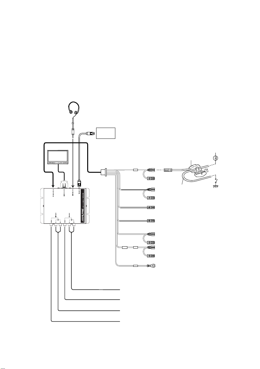
System Connections
TME-M710
(North American Model Only)
TO CONTENTS
- 6 -
Make connections correctly.
Improper connections may cause a fire or operation failure.
Basic connection
p
u
1
a
s
w
q
e
i
;
o
2
t
3
4
5
6
8
d
f
g
h
7
9
q
r
Battery
y
Chassis
Page 7

1 Foot brake lead (Yellow/Black)
TME-M710
TO CONTENTS
- 7 -
2 Hand brake lead (Yellow/Blue)
3 Dimmer lead (White/Blue)
45
6 Reverse Lead (Orange/White)
7 ACC power lead (Red)
8 Fuse (7.5A)
9 Ground lead (Black)
p Foot brake lamp
q Brake connector (Included)
w Foot brake lead
e Foot brake switch
r Hand (parking) brake lamp
t Hand (parking) brake lead
y Hand (parking) brake switch
u Headphone
i Main monitor
o Connection cable
; RGB cable
a To RGB output terminal
s Made by Alpine navigation
d Audio input connectors (AUX 1)
f Video input connector (AUX 1)
Connect this lead to the foot brake lead powered
when the foot brake is pressed.
Connect this lead to the hand brake lead
powered when the hand brake is pulled.
This lead may be connected to the vehicle’s
instrument cluster illumination lead. This will
allow the backlighting of the unit to dim whenever
the vehicle’s lights are turned on.
Remote control output lead (White/Brown)
To remote control input lead of ALPINE products
used in the system.
Use only when a back-up camera is connected.
Connect to the plus side of the car’s reverse
lamp that lights when the transmission is shifted
into reverse (R).
Switches the video picture to the back-up
camera. This is linked with putting the car into
reverse (R).
To ACC power lead powered when engine key
position is ACC.
Connect the lead to a good chassis ground on
the vehicle. Make sure the connection is made to
bare metal and is securely fastened using the
sheet metal screw provided.
If the cable is too short, use the extension cable
(KWE-664N, sold separately).
Use these connectors to input the audio signals
from a DVD player, video deck etc.
Use this connector to input the video signals
from a DVD player, video deck etc.
g Audio input connectors (AUX 2)
Use these connectors to input the audio signals
from a DVD player, video deck etc.
h Video input connectors (AUX 2)
Use this connector to input the video signals from
a DVD player, video deck etc.
• When connecting a rear view camera, use the “AUX
IN 2”.
To prevent external noise from entering the
audio system.
• Locate the unit and route the leads at least
10cm away from the car harness.
• Keep the battery power leads as far away from
other leads as possible.
• Connect the ground lead securely to a bare
metal spot (remove the coating if necessary)
of the car chassis.
• If you add an optional noise suppressor,
connect it as far away from the unit as
possible. Your Alpine dealer carries various
Alpine noise suppressors, contact them for
further information.
• Your Alpine dealer knows best about noise
prevention measures so consult your dealer for
further information.
FR
ES
DE
IT
SE
Page 8
(General Foreign Model Only)
TME-M710
TO CONTENTS
- 8 -
Make connections correctly.
Improper connections may cause a fire or operation failure.
Basic connection
e
u
i
r
t
y
1
2
3
4
5
7
o
;
a
s
6
8
p
q
9
w
Page 9

1 Parking brake lead (Yellow/Blue)
TME-M710
TO CONTENTS
- 9 -
2 Dimmer lead (White/Blue)
34
5 Reverse Lead (Orange/White)
6 ACC power lead (Red)
7 Fuse (7.5A)
8 Ground lead (Black)
9 Parking Brake Lamp
p Brake Connector (Included)
q Parking Brake Signal Lead
w Parking Brake Switch
e Headphone
r Main monitor
t Connection cable
y RGB cable
u To RGB output terminal
i Made by Alpine navigation
o Audio input connectors (AUX 1)
; Video input connector (AUX 1)
a Audio input connectors (AUX 2)
s Video input connectors (AUX 2)
Connect this lead to the parking brake lead
powered when parking brake is pulled.
This lead may be connected to the vehicle’s
instrument cluster illumination lead. This will
allow the backlighting of the unit to dim whenever
the vehicle’s lights are turned on.
Remote control output lead (White/Brown)
To remote control input lead of ALPINE products
used in the system.
Use only when a back-up camera is connected.
Connect to the plus side of the car’s reverse
lamp that lights when the transmission is shifted
into reverse (R).
Switches the video picture to the back-up
camera. This is linked with putting the car into
reverse (R).
To ACC power lead powered when engine key
position is ACC.
Connect the lead to a good chassis ground on
the vehicle. Make sure the connection is made to
bare metal and is securely fastened using the
sheet metal screw provided.
If the cable is too short, use the extension cable
(KWE-664N, sold separately).
Use these connectors to input the audio signals
from a DVD player, video deck etc.
Use this connector to input the video signals
from a DVD player, video deck etc.
Use these connectors to input the audio signals
from a DVD player, video deck etc.
Use this connector to input the video signals
from a DVD player, video deck etc.
To prevent external noise from entering the
audio system.
• Locate the unit and route the leads at least
10 cm away from the car harness.
• Keep the battery power leads as far away from
other leads as possible.
• Connect the ground lead securely to a bare
metal spot (remove the coating if necessary)
of the car chassis.
• If you add an optional noise suppressor,
connect it as far away from the unit as
possible. Your Alpine dealer carries various
Alpine noise suppressors, contact them for
further information.
• Your Alpine dealer knows best about noise
prevention measures so consult your dealer for
further information.
• When connecting a rear view camera, use the “AUX
IN 2”.
Page 10
TME-M710
TO CONTENTS
- 10 -
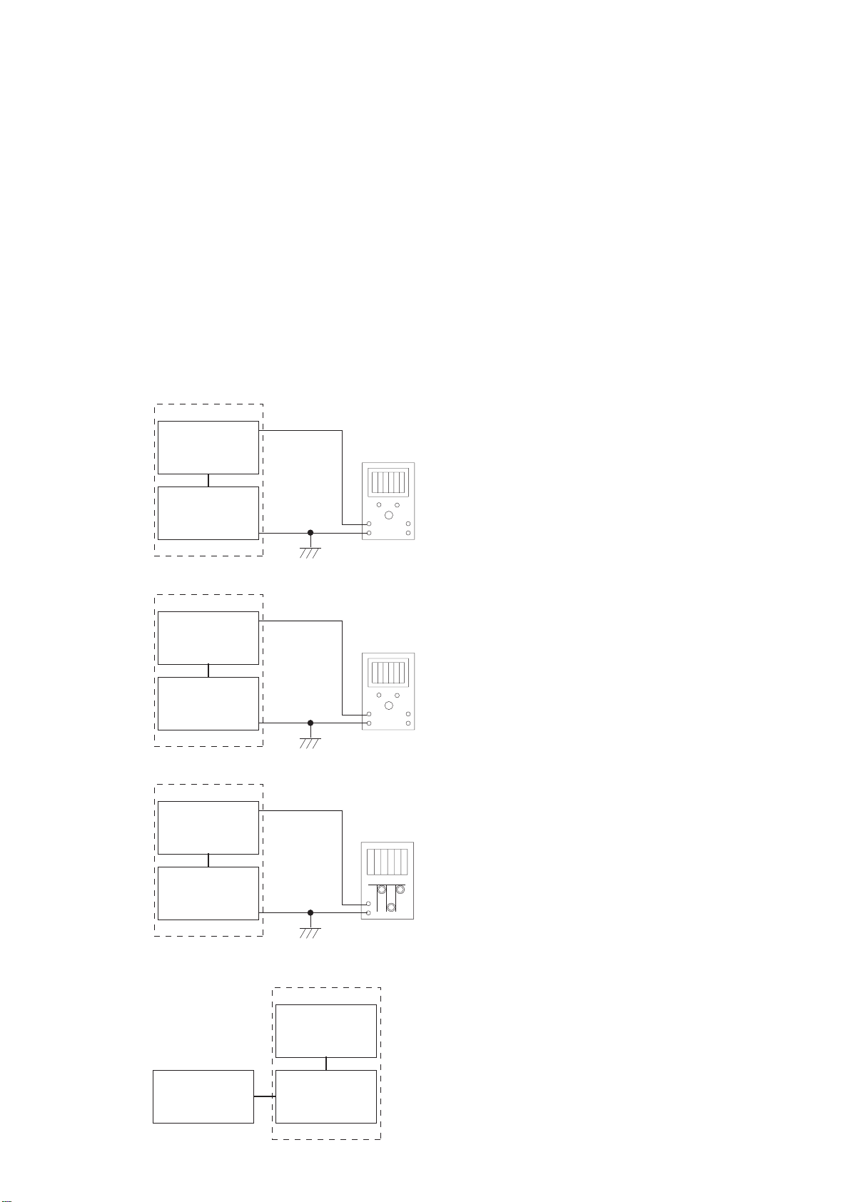
Adjustment Procedures
1. Preparation product :
* TME-M770 and NAVIGATION (North American : NVE-N872A, General Foreign : NVE-N099P) are needed for adjustment.
2. Cancellation of AUX Regulation (Parking Wire)
(North American Model Only)
(1) HAND : L <GND> (ON), FOOT : H <14V> (ON)...by initial setting
(2) HAND : H <14V> (OFF)
(3) HAND : L <GND> (ON)
(4) FOOT : L <GND> (OFF)
3. VIDEO Adjustment
(1) Connection
TME-M710
MONITOR Unit
TP540(VSS)
DC Volt Meter
(General Foreign Model Only)
(1) Parking Brake : L <GND>
GND
AV Interface Unit
TME-M710
MONITOR Unit
TP529(VGH)
GND
AV Interface Unit
TME-M710
MONITOR Unit
TP549(HSYNC)
GND
AV Interface Unit
+
-
Figure 1
DC Volt Meter
+
-
Figure 2
Frequency Counter
+
-
Figure 3
NAVIGATION
NVE-N099P or NVE-N872A
<Map information is displayed. >
TME-M710
MONITOR Unit
RGB-IN
AV Interface Unit
Figure 4
Page 11
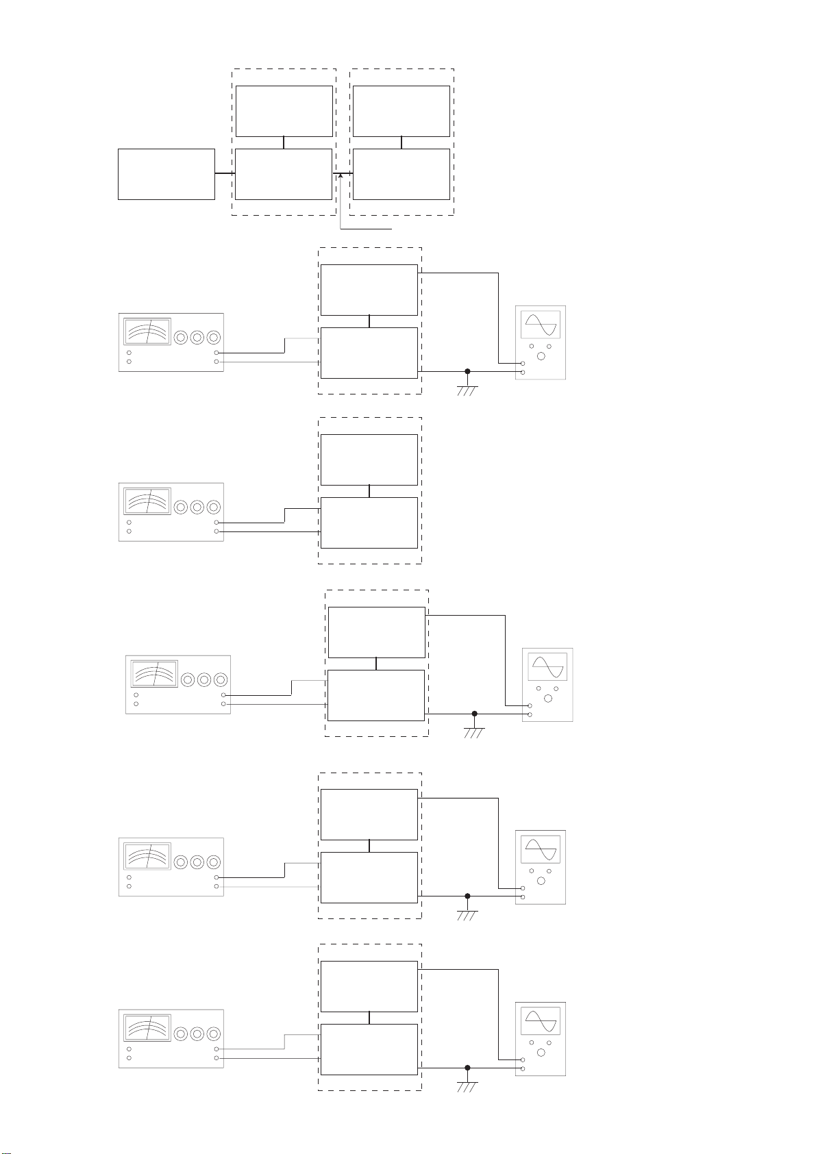
TME-M770
TO CONTENTS
- 11 -
TME-M710
TME-M710
MONITOR UnitMONITOR Unit
NAVIGATION
NVE-N099P or NVE-N872A
<Map information is displayed. >
+
-
Pattern Generator
(10STEP SIGNAL : NTSC)
+
-
Pattern Generator
(10STEP SIGNAL : NTSC)
RGB-IN AUX-OUT
AUX-IN
AV Interface UnitAV Interface Unit
TME-M710
MONITOR Unit
TP525(VCOM)
AUX IN
GND
AV Interface Unit
TME-M710
MONITOR Unit
AUX IN
GND
AV Interface Unit
TME-M710
MONITOR Unit
TP530(GREEN)
Figure 5
COMPOSITE SIGNAL
GND
GND
Figure 7
Oscilloscope
+
-
Oscilloscope
Figure 6
+
-
Pattern Generator
(10STEP SIGNAL : NTSC)
+
-
Pattern Generator
STEP13 : (10STEP SIGNAL : NTSC)
STEP14 : (PAL COLOR BAR)
+
-
Pattern Generator
(PAL COLOR BAR)
AUX IN
GND
AV Interface Unit
TME-M710
MONITOR Unit
TP528(RED)
AUX IN
GND
AV Interface Unit
TME-M710
MONITOR Unit
TP532(BLUE)
AUX IN
GND
AV Interface Unit
GND
GND
GND
+
-
Oscilloscope
+
-
Oscilloscope
+
-
Figure 8
Figure 9
Figure 10
Page 12

(2) Adjustment Procedures
TO CONTENTS
- 12 -
NOTE : NAVIGATION(*) = North American : NVE-N872A, General Foreign : NVE-N099P
Step Operations Process
Connection
Test Point/
P.W.Board
Coordinates
TME-M710
Adjustment
AUX terminal
1
2
VSS Voltage Adjustment
VGH Voltage Adjustment
3
HSYNC Frequency Adjustment
4
NAVI Screen Adjustment (1)
5
NAVI Screen Adjustment (2)
6
Switching MODE1 and setting DIAG Mode
7
Figure 1 to 3
Figure 1
Figure 2
Figure 3
Figure 4
Figure 5
Figure 6
TP540
(4-E)
TP529
(4-E)
TP549
(4-E)
Confirm AUX terminal OPEN.
Adjust by VR501 so that it may be set to
-16V+0.05, -0.05.
Adjust by VR500 so that it may be set to
+13V+0.05, -0.05.
Adjust by VR504 so that it may be set to 15.73KHz.
(1) After connecting NAVIGATION(*) and TME-M710,
switched NAV. Mode.
(2) Monitored NAVI position adjustment screen by
TME-M710.
<NAVIGATION (*) Screen position setting value :
“X=-2, Y=00”>
(3) Adjust by VR503 so that a white line may be
visible to right and left of NAVI position adjustment
screen.
(1) After connecting NAVIGATION(*) and TME-M770,
inputed Composite Signal to TME-M710 AUX-IN1.
(2) Monitored NAVI position adjustment screen by
TME-M710.
<NAVIGATION(*) Screen position setting value :
“X=00, Y=00”>
(3) Switched AUX1 Mode (TME-M710).
(4) Switched MODE2 by pushing long DISP Key.
(5) Adjust by VR505 so that a white line may be
visible to right and left of NAVI position adjustment
screen.
(1) Switched MODE1 by pushing long DISP Key.
(2) Inputed 10STEP SIGNAL NTSC to AUX-IN 1
(TME-M710).
(3) After pushing long POWER Key, pushed VOLUME
Down Key and VOLUME Up Key in an order.
(Setting DIAG Mode)
8
COM AMP Adjustment
9
COM DC Adjustment
10
BRIGHT Adjustment
11
CONT-RGB 2 Adjustment
12
NTSC TINT Adjustment
13
PAL COLOR Adjustment
14
PAL TINT Adjustment
Figure 6
Figure 7
Figure 8
Figure 7
Figure 9
Figure 9
Figure 9
TP525
(4-E)
TP530
(4-F)
TP528
(4-F)
TP528
(4-F)
TP528
(4-F)
Adjust to 6.5Vp-p by VOLUME Up/Down Key as
becoming the waveform of Figure 11.
Adjust by VOLUME Up/Down Key so as that flicker of
screen may disappear.
Adjust to black color should be set to “0 level” by
VOLUME Up/Down Key as becoming the waveform
of Figure 12.
Adjust by L508 so that outside frame of H characters
shown in Figure 13 may become black.
(1) Switched NTSC COLOR BAR.
(2) Set up NTSC COLOR value “65” by VOLUME Up/
Down Key.
(3) Adjust by VOLUME Up/Down Key as becoming the
waveform of Figure 14.
(1) Switched PAL COLOR BAR.
(2) Adjust by VOLUME Up/Down Key as becoming the
waveform of Figure 15.
Adjust by VOLUME Up/Down Key as becoming the
waveform of Figure 15.
Page 13

Step Operations Process
TO CONTENTS
- 13 -
Connection
Test Point/
P.W.Board
Coordinates
TME-M710
Adjustment
PAL PHASE Adjustment
15
16
Cancellation DIAG Mode
Figure 11
Figure 10
Figure 10
TP532
(4-F)
Adjust by VOLUME Up/Down Key as becoming the
waveform of Figure 16.
Cancelled DIAG Mode by Pushing POWER Key at
DIAG Mode.
Figure 12
Figure 13
Page 14

Figure 14
TO CONTENTS
- 14 -
TME-M710
Figure 15
Figure 16
Page 15

Extension Cable
TO CONTENTS
- 15 -
*Always connect the Extension Cable when making checks of voltage and repair.
< Monitor Unit >
LCD Display
TME-M710
KEY P.W.Board
MONITOR P.W.Board
CB900
32PIN
CB504
CB500
(1)
(2)
(1) 01E37339S01
(2) 01E37341S01
Page 16

< Monitor Unit >
TO CONTENTS
- 16 -
TME-M710
Block Diagram
Parts Layout on P.W.Boards and Wiring Diagram
Schematic Diagram
Terminal Voltage of IC/TR
18 , 19
20 , 21
22 to 24
Exploded View (Cabinet)
17
25
NOTE : Due to continuing product improvement, specifications and designs are subject to
change without notice.
Page 17

Block Diagram
TO CONTENTS
- 17 -
ACC+5V
REMSEN
KEY
GND
GND
DIMMER
GND
SHIELD-GND
RGB/VIDEO
1
S-GND
2
3
RGB
4
5
NTSC/PAL
6
CS_DECODER
7
CS_DAC
8
SLK
9
DI
10
CS_OSD
11
KEY
12
REMSEN
13
ACC+9V
14
P-GND
15
BL-PWM(BL-OFF)
16
BL +9V
17
BL-GND
18
P.GND
19
20
SP-OUT
REMO-CON
RECEIVER
ICC:Max1mA
BUFFER
BUFFER
BUFFER
BUFFER
BUFFER
DIMMER
POW
IND.
DAC
OSD
BUFFER
KEY
POW-CTL
VGH-CTL
VGL-CTL
V-MUTE
MODE1, 2
OSD RESET
ACC+9V
3.58
MHz
4.43
MHz
RGB
VSH,V5B
ACC+5V
REG.
ACC+3.3V
REG.
PWR+5V
REG.
DC/DC
CONVERTER
ACC+5V
P.SAVE
Vcc1
CHROMATIC
CIRCUIT
TME-M710
ACC+5V
ACC+3.3V
VSH,V5B
-16V
+13V
-11V
-10V
ICC1:58mA
13V
ICC2: 6
mA
ICC3:1.5mA
Vcc2
Vcc3
SYNCOUT
BLKIN
TC
7SH
32FU
Hsync
NTSC/PAL
MDW, MDN
SYNI
VCS
HSY
VSY
TC7S
66FU
CONTROL
CIRCUIT
TFT
+5V
RGB
VDD
-11V
-10V
ISH:60mA
IGH:1mA
IGL:-1mA
ICC:1mA
ISS:-1mA
IDD:15mA
+5V +13V
-10V
VGH
VGL
VSH
LCD
PANEL
UNIT
ACC+9V
BACK
LIGHT
INVERTER
IL=6mArms(Max6.5)
VL7:660Vrms(Max730)
WL:4.29W
-11V
-16V
VCC
VSS
Page 18

Parts Layout on P.W.Boards and Wiring Diagram(1/2)
TO CONTENTS
- 18 -
KEY P.W.Board
(Foil Side View)
TME-M710
1
2
4
3
LCD504
ASSY,LB065WQ2
(Bottom Side View)
To CB504
32 1
Caution:The part marked with is generating a high voltage,
so care will be necessary when working.
WHT
PNK
1 2
B
MONITOR P.W.Board
(Component Side View)
Q509
R616R613
C598
C597
Q508
BE EB
R577
TP548TP547TP546
C576
R588
IC508
R552
R634
C582
R553
R589
C580
R571
C550
RA505
XL501
C615
R533
E513
ZD503
R536
R578
C574
C566
R566
C565
R538
C573
R573
R633
EB
C546
XL500
R574
C548
R550
Q512
R575
R576
R527
R528
R541
R544
C545
C535
R529
R546
C547
R556
SD501
D507
C592
C593
C594
ZD500
VR504
B
Q500
L512
C603
SD500
VR501
R542
R547
VR502
R612
R607
R606
C595
R608
C596
C600
R618
C591
R605
R617
L514
1 32
C543
R532
R524
C538
C536
R526R525
C534
VR500
R535
R540
C544
IC507
R543
R545
C549
EBE
E504
Q501
L510 L509
E506 E505
R602
C588
IC509
VR505
31
54
IC513
A
SD502
CB504
R581
R587
R582
R586
C578
VR503
C532
R585
R580
RA502
TP534
C589
E512
E511
E501
C529
R583
C608
L506
RA501
F500
C523
4
3
C577
51
IC510
R590
L513
L511
C575
E510
E508
E509
CB500
R564
C561
R508
R511
IC504
R523
R522
IC505
IC503
ZD502 ZD501
T500
C533
C530
C526
C525
C524
RA503
R512
C540
C539
L508
IC506
C537
C518
R519
C519
R516
R515
C520
E502
D502
D503
D504
D501
D500
To AV Interface Unit
(B.BOX P.W.Board (CB101))
C500
D515
CB501
KEY P.W.Board
(Component Side View)
2 1
To CB503
2
CB503
1
IC502
IC501
C511
C509
IC512
SP502
CB502
21
SPEAKER, 8ohm-1W
RED
12
BLK
To CB502
R500
R904
2
1
SW900
R901
R902
ZD900LD900
34
IC900
R906
R909
R908
R907
Q901
SW901
SW904SW903 SW902
R903
R905
TP905
E900
TP904
CB900
TP902
TP903
TP901
5
A
To CB500
17
To CB900
17
Orange Color Pattern:Component Side Pattern
Blue Color Pattern:Foil Side Pattern
FGEDCB
Page 19

Parts Layout on P.W.Boards and Wiring Diagram(2/2)
TO CONTENTS
- 19 -
1
MONITOR P.W.Board (Foil Side View)
TME-M710
2
4
3
C528
C522
C516
C515
C506
TP504
L505
TP503
TP502
C505
C531
C521
C517
C514
C513
C512
C504
C502
TP508
TP501
TP506TP505
TP523
TP507
TP552
TP551
TP522
TP520
TP521
TP512
TP519
TP513
C501
TP514
TP515
TP516
RA504
R505
C503
R506
R507
R509
TP517
C542
C541
C527
R510
R539
C558
C553
C551
C555
R537
C557
E514
R534
C556
R520
C560 C559
R517
R502
C590
5
Q507
32
R604
Q505
R518
R561
EB
C613
R635
C612
1
R603
R503
R501
L515
Q506
R504
Q511
EB
E
B
R549
R548
R632
L516
TP518
TP510
TP509
TP511
TP529
C587
C585
C584
R623
R621
C607
TP531
TP529
C579
TP550
TP549
TP525
TP536
TP533
TP535
C581
C586
TP539
TP537
TP525 TP540TP549
C563
C583
TP540
R631
C554
R558
Q504
23
15
TP524
TP542
TP526
TP543
TP527
C614
TP544
TP538
TP530
TP532
C570
C571
RA500
TP545
TP541
TP528
C567
C569
C572
RA506
5321
Q503
C568
R570
C602
C599
R625
R569
R567
R568
R513
R514
R615
C601
R624
R565
R626
B
C609
C610
R627
C562
BE
R560
R559
R557
R630
C552
C604
R614
43
IC511
Q510
E
C611
C564
Q502
15
R622
R609
R611
R610
R619
R620
C605
C606
VD500
TP528
TP530
TP532
5
A
Orange Color Pattern:Component Side Pattern
Blue Color Pattern:Foil Side Pattern
FGEDCB
Page 20

C500 0.01
TO CONTENTS
TO PARTS LIST
TO P. W. BOARD
- 20 -
CB500
CONN,FFC-7P
CB501
CONN, CSS5020-20P
IC512
BA05SFP
33k
2.2k
R532
R535
27k
R543
12k
2.2k
C544
IC502
BA05SFP
C534 0.1
L505
2.2u
IC501
NJM2880U33
C509 0.01
C506 0.1
C502 10
C504 10
TP511
TP509
TP510
TP518
D515
1SS355
TP513
TP514
TP515
TP516
TP512
TP519
TP520
D500 1SS355
D501 1SS355
C512 10
C513 10
C514 0.1
0.01
C511
47k
RA504
C515 0.01
R505 47k
R509 10k
R510 10k
C517 10
C521 10
C516 0.022
C519 1000p
C520 1000p
C518 0.1
C522 0.1C523 0.1
IC506
NJU3713AV
C531 N.U.C532 N.U.
C528 0.1C529 0.1
C505 10
L506
2.2u
E501
100/6.3
R519
1k
560
560
R516
R515
1k
R512
C524 1000p
C525 1000p
C526 1000p
C530 1000p
VR500
220k
R525
R524 68k
C536 0.22
IC507
AN8018SA
C535 0.1
R526 10k
C538 390p
R527 2.7k
R528 10k
R529 68k
C501 10
E502 100/16
C537 0.1
560
RA503
C533
1000p
R540
C543 2.2
R541
VR501
22k
R545
0.01
R565
4.7k-F
LCD504
CB504
CONN,FFC-32P
ASSY, LB065WQ2
C567 1
C568 1
C563 0.1
C564 1
C562 220p
R569 10k-F
R567
18k-F
C569
10
R570
30k-F
C570
R568
10
12k-F
R513
5.6k-F
C571
10
N.U.
VR502
C572
10
R514
4.7k-F
TP549
TP550
TP534
R582
100
C578
470p
RA502 100
C581 10
C579 10
R583 100
R580 10k
R581 N.U.
0.1
C577
IC510
TC7SH32FU
R586
C583 0.1
R585 N.U.
47k
100k
VR505
R587 10k
RA501
560
22k
R590
IC513
TC7S66FU
C586
82p
100k
VR503
C587 33p
C584 1000p
C585 1000p
C588 0.1
IC509
LZ9GH29
100
RA506
100
100
R602
RA500
C591 0.22
R605 220k
SD500
MA716
560k
C603
1000p
33p
C600
C599 1
C602 0.022
IC511
NJM2107F
R614
68k
C601 560p
R615 1M
R604
R617
560k
R618
8.2k
R619
R620
5.6k
ZD500
2.2k
VR504
MAZS0510M
C605 0.1
0.1
R622
C606 0.1
C609
VD500
1000p
MA335-TX
L514
C610
2.7u
18k
R621
68
100p
C607 0.022
R623 13k
TP524
TP525
TP526
100
R626
2.7k
R624
Q510
2SC2411K
3.3k
R625
C611 330p
R627 330
TP529
TP531
TP533
TP535
TP536
TP537
TP538
C608 N.U.
TP539
TP540
TP527
TP541
R606
1M
R608
390
C592 0.1
C593 0.1
C594 10
C595 220p
D507
R609
R607
47k
R612
24k
L512
15u
33p
C596
MA2S111
3.6k
R610
68k
R611
5.6k
Q501
2SC4540
2SA1735
SB05-05CP
L509
470u
L510
330u
Q500
SD501
SD502
SB05-05CP
E505 330/25
E506 330/25
R630 16k
C552 0.01
1k
R556
560
C549 0.1
E504 100/16
1k
R547
R544
560-1/4
0.01
C545
10k
68k
0.1
R546
R542
C547
68k
Q504
XN1A311
R558
1
C554 0.01
R631 1.2k-1/4
R557
1
Q502
2SD1782K
22k
R559
22k
R560
Q503
XN1A312
SP502
SPEAKER, 8ohm-1W
TP501
TP502
TP503
TP504
TP505
CB502
CONN,WTB-02P
R500
TP507
TP508
1k
TP521TP506
TP522
TP523
D502 1SS355
D503 1SS355
D504 1SS355
C527 0.1
R506
10k
R507 10k
R508 10k
ZD501
ZD503
MAZS056M
MAZS056M
R511
IC503
C541 0.1
TC74VHC14FT
ZD502
MAZS056M
IC504
2.2k
MB90097PFV
10k
R522
L508
FSDV
C540
27p
N.U.
R523
C539
27p
TP517
IC505
TC74VHC14FT
L515
R548 1k
R549 N.U.
C612 N.U.
C546
C548 1
R550 270
N.U.
E513 47/16
R552 18k-F
C550 0.1
R553 10k
RA505
100
R533 3.9k
R536 3.9k
R538 3.9k
Q512
DTA124EKA
C503 10
C542 0.1
R534 1.2k
R537 1.2k
R539 1.2k
R632
10k
2.2
0
R633
N.U.
R634
0.01
C551
C553 0.01
C555 0.01
C556 0.01
R635 560
Q511
2SC2412K
R501
47k
IC508
RB5P0090M
C557 0.01
C558 0.01
E508 10/16
C561 0.1
R564 10k
C613 10
C559 1
560
R503
N.U.
R561
R518 2.7k
1k
82p
C560
R504
R520
47k
10
E514
R502
R517
39 1/4
36 1/4
E510
E509 100/16
47/16
L516
2.2u
TP546
TP547
TP548
C573 0.1
R573 75
R574 75
R575 75
R576 1k
R577 1k
R571 1.8k
C574 0.1
C565 1
C566 6800p
R566 1M
C575 3p
XL500
4.43MHz
C576
3p
XL501
3.57MHz
C615
0.01
1M
R578
5.6k
R588
C582
0.47
0.01
C580
8.2k
R589
L511
100u
F500
1.6A
R603
Q505
DTC124EKA
E511 100/16
E512 100/16
C589 N.U.
10k
Q506
DTC124EKA
2.7k
R604
Q507
FMY1A
0.1
C590
R613
L513 68u
C597 0.18
820-1/4
2SD1760
C598
Q508
N.U.
T500
TP551
TP552
CB503
CONN,WTB-2P
Q509
2SD1760
R616
BLC4115
820-1/4
C614 100p
TP528
TP530
TP532
TP542
TP543
TP544
TP545
Page 21

CB900
TO CONTENTS
TO PARTS LIST
TO P. W. BOARD
- 21 -
CONN, FFC-7P
TP901
TP902
TP903
TP904
TP905
R909
R901
2.7k-1/4-F
SW900
SKRPACE010E2
R902
3.9k-1/4-F
SW901
SKRPACE010E2
R903
8.2k-1/4-F
SW902
SKRPACE010E2
R905
27k-1/4-F
SW903
SKRPACE010E2
R906
47-1/4F
SW904
SKRPACE010E2
R904
E900 10/16
IC900
RS-181
1k
Q901
DTC124EE
R907
82 1/4
R908
47 1/4
180 1/4
LD900
ZD900
SML512BC2T
MAZS0560M
Page 22

TME-M710
TO CONTENTS
TO SCHEMATIC
- 22 -
Terminal Voltage of IC/TR
Ref.No. Pin No. Voltage (V) MODE Ref.No. Pin No. Voltage (V) MODE
1 9 8 3.3
2 0 9 0
IC501
IC502
IC503
IC504
IC505-1
3 1.3 10 3.3
4 3.3 11 0
5 9 12 3.2
1 4.9 13 0.3
2 9 14 3.3
3 0 1 0
4 5 2 5
5 0 3 5
1 0.6 4 5
2 5 5 0
3 0.6 6 0
4 0 7 5
5 0.6 8 0
6 5 9 0
7 0.3 10 0
8 0 11 5
9 5 12 5
10 0.3 13 5
11 4.8 14 5
12 5 15 0
13 0.6 16 0
14 5 17 0
1 3.3 18 5
2 3.3 19 5
3 3.3 20 5
4 0 1 0.5
5 3.3 2 0
6 3.3 3 0.6
7 1.6 4 0.6
8 1.6 5 0.3
9 0 6 0.6
10 0 7 7.9
11 0 8 0
12 0 9 9.1
13 0 10 0
14 0 11 0
15 0.3 12 1
16 0.3 13 1
17 0.3 14 0.8
18 0.3 15 1.7
19 3.3 16 1.3
20 3.2 1 4.8
1 0.6 2 0
2 3.3 3 5
3 0.6 4 2.1
4 3.3 5 3.6
5 0.6 6 0.5
6 3.3 7 0
7 0 8 1.3
IC505-2
IC506
IC507
IC508-1
Page 23

TME-M710
TO CONTENTS
TO SCHEMATIC
- 23 -
Ref.No. Pin No. Voltage (V) MODE Ref.No. Pin No. Voltage (V) MODE
9 5 15 5
10 4.7 16 5
11 0 17 0
12 5 18 0
13 2.6 19 0
14 2.6 20 5
15 2.6 21 5
16 2.6 22 5
17 2.6 23 0
18 2.6 24 5
19 0.9 25 0
20 2.2 26 5
21 2.7 27 0
22 2.4 28 0
23 0 29 0
24 0 30 0
25 2.5 31 0
26 4.2 32 5
27 2.9 33 5
IC508-2
IC509-1
28 2.5 34 0
29 4.2 35 0
30 3 36 2.5
31 0 37 0
32 0 38 2.7
33 2.5 39 5
34 2.5 40 0
35 2.5 41 0
36 5 42 0
37 1.9 43 2.5
38 0 44 2.5
39 6.4 45 5
40 13 46 0
41 2.6 47 2.2
42 2.5 48 0
43 5/0 NTSC/PAL 49 0
44 0 50 4.9
45 0.2 51 5
46 5 52 5
47 5 53 5
48 5 54 0
1 0.3 55 0
2 0.3 56 0
3 4.8 57 3.5
4 2.5 58 4
5 0 59 0
6 2.5 60 5
7 0 61 0
8 5 62 0
9 0 63 5
10 0 64 0
11 0.2 65 4.9
12 5 66 0
13 5 67 0
14 0.2 68 0
IC509-2
Page 24

TME-M710
TO CONTENTS
TO SCHEMATIC
- 24 -
Ref.No. Pin No. Voltage (V) MODE Ref.No. Pin No. Voltage (V) MODE
69 0 1 0
IC509-3
IC510
IC511
IC512
IC513
IC900
Ref.No. Pin No. Voltage (V) MODE
Q500
Q501
Q502
Q503
70 2.6 2 13
71 2.5 3 13
72 0 4 4.8
1 0 5 0
2 5 E 0
3 0 B 4.6
4 5 C 0
5 5 E 0
1 2.7
2 0
3 2.7
4 2.7 2 0
5 5
1 9
2 0
3 1.3
4 5 B -0.5
5 9
1 2.5
2 2.5 B -0.4
3 0
4 0
5 5 B 2.7
1 4.8
2 0
3 0 B 3.9
4 5
E 9.1
B 8.7 B 5/0
C 0
E 0
B 0
C 9
E -16
B -15.4
C -16
1 0
2 5
3 5
4 0
5 0
Q504
Q505
Q506
Q507
Q508
Q509
Q510
Q511
Q512
Q901
B
C
1
3
4
5
E
C
E
C
E
C
E
C
E
B 3.6
C
E
C
8.8
8.8
0.2
8.7
0.2
8.7
2.3
4.4
3.2
3.6
0/0
0/3.8
0
9
0
0
5
0
DIMMER
ON/OFF
[Measuring Conditions]
1. Power Supply Voltage : DC14.4V
2. Measuring Meter : Digital Multimeter
3. Measuring Point Reference : Between GND
4. Measuring Condition : See each data
Page 25

Exploded View (Cabinet)
TO CONTENTS
TO PARTS LIST
- 25 -
(Monitor Unit)
7
8
9
10
TME-M710
SP502
1
11
17
X3
a
2
LCD504
3
4
20
a
2
CB501
18
15
X2
15
X2
12
13
X4
16
14
X4
14
X2
Page 26

< AV Interface Unit >
TO CONTENTS
- 26 -
TME-M710
Block Diagram
Parts Layout on P.W.Board and Wiring Diagram
28 , 29
Schematic Diagram
Terminal Voltage of IC/TR
Description of IC Terminal
31 to 33
34 , 35
Exploded View (Cabinet)
27
30
36
NOTE : Due to continuing product improvement, specifications and designs are subject to
change without notice.
Page 27

Block Diagram
TO CONTENTS
- 27 -
TME-M710
R SU
POWE PPLY
NAVI INPUT
AUX
IN_1
AUX
IN_2
GND
ACC
REVERSE
P-BRAKE
H-BRAKE
F-BRAKE
ILUM
PROTECTION
REMOUT1
REMOUT2
REMOUT3((NAVI)
GUID CTL
NRGB
RGB
C.SYNC
VIDEO
AUDIO
VIDEO
L,R
VIDEO
L,R
CIRCUIT
ISO
AMP
ISO
AMP
ISO
AMP
ISO
AMP
ISO
AMP
SW
5V
REG.
RESET
VIDEO
SELECTOR
SELECTOR
VOUT1
AUDIO
AUDIO 9V
REG.
Navi SYNC
/VIDEO
Switching
CONVERTER
9V REG.
REM 1
REM 2
REM 3
Navi INT
V_SEL 1
V_SEL 2
A_SEL 1
A_SEL 2
GUID CTL
NRGB
EEPROM
BUFFER
A+9V
SHIELD-GND
C.SYNC/VIDEO
S-GND
5V
REG.
u-COM
BL-PWM
V
NAVI/ IDEO
SCL
SDA
BEEP(PWM)
NAVI-VOL
SP-VOL
RGB
RGB
NTSC/PAL
CS-DECORDER
CS-DAC
CLK
DI
CS-OSD
KEY IN
REMSEN
ACC+9V
P-GND
BL-PWM
BL+9V
BL_GND
SP_GND
SP-OUT
1
2
3
4
5
6
7
8
9
10
11
12
13
14
15
16
17
18
19
20
BPF
A+9V
Volume
SP AMP
E-VR + H.PHONE AMP
A+9V
HEAD
PHONE
OUTPUT
Page 28

Parts Layout on P.W.Boards and Wiring Diagram(1/2)
TO CONTENTS
- 28 -
1
B.BOX P.W.Board (Component Side View)
To Monitor Unit
(MONITOR P.W.Board (CB501))
TME-M710
2
4
3
ZD114
ZD111
L105
E168
E163
R248
R249
L103
L102
CB100
C169
E167
IC116
TP110
CB101
E169
ZD105
ZD104
ZD115
C148
R240
IC119
E166
IC112
E159
E162
ZD107
R239
ZD106
C124
R246
CB102
E136
E137
E138
E111
JK101 JK100
R235
B
Q130
E
IC113
RA103
IC111
Q121
45
21
IC107
E112
R241
3153
R218
C146
RA105
R230
E160
ZD103
D100
C144
R217R216
E117
ZD116
IC114
C123
E147
E131
R261
R138
C149
E118
R244
B
Q131
E
ZD110
RA107
C151
XL100
R165
C116
C117
R166
ZD113
B
Q129
R259
E
B
Q126
E
B
Q127
E
B
Q128
E
B
Q125
E
IC117
R233
R234
RA104
R227
R226
RA108
RA101RA100
E
Q115
B
C150
C139
E139
E123 E122
E120
C120
R175 R174
R136
R137
IC101
R147
R148
R176
C121
TP108
R242
R245
R243
R237
R236
E165
C135
IC110
C122
R146
R145
R144
R143
R173
C119
C115
R164
R163
C114
E101
E104 E103 E102
E100
E124
E113
R177
E107
R180
E108
E109
E110
JK102
R169
R159
B
Q108
E
C112 C111 C110
R135 R133 R131
B
BE
R113
R112
R105
R104
B
Q101
E
B
Q102
E
B
Q103
E
E125
E114
R152
R151
E
Q104
R128
Q100
B
Q105
E
R139
TP120
B
Q106
E
R140
TP121
B
Q107
E
R141
IC106
R256
R247
C109
R129
TP119
E170
Q109
R160
E171
R161
E172
TP122
E119
R154
Q110
R156
Q111
R162
R158
E115
R124
E
B
E
B
R171 R170
E
B
E106
C118
R181
R184
R172
E148
R187
R186
E105
R167
E116
3
4
IC100
51
E121
E154
R123
R142
R149
E155
Q113
53
Q114
R190
E132
R264
DIN100
E143
E
B
R268
E152
21
B
Q116
E
R265
R231
E145
IC108
2
Q119
IC109
IC105
R185
R238
C129
E157
3
51
ZD100
ZD101
ZD102
R168
E144
E146
E156
E142
C130
E158
5
A
Orange Color Pattern:Component Side Pattern
Blue Color Pattern:Foil Side Pattern
FGEDCB
Page 29

Parts Layout on P.W.Boards and Wiring Diagram(2/2)
TO CONTENTS
- 29 -
1
B.BOX P.W.Board (Foil Side View)
TME-M710
2
4
3
C137
R127
R126
R125
C140
TP130TP129
TP127 TP126
TP124
B
R260
R193
R206
R195
R189 R188
R222
R209
R212
Q120
Q118
TP123
Q112
E
R225
R207
TP133TP132
C178
C136
R211
C138
Q132
EB
C141
TP128
BE
C113
R214R213
C142
TP116
Q117
R117
R132
R215
R210
C106
R150
R114
C143
R153
R130
R155
R157
R199
TP103
C102
TP148
R270
R269
C108
R120
R134
R262
C126
TP112
R115
R118
R119
R121
C134
R203
R192
TP101
R116
R122
R202
C125
C104
C127
C132
R191
R100
R101
R198
TP149
TP131
TP113
TP114
TP125
TP111
R106
R107
TP115
R110
R111
TP100
C100
TP106
TP152
TP151
TP150
TP159
TP166
R108
R109
C164
R204
R179
R178
R205
C163
R201
R194
R250
C177
TP158
TP153
R251
R200
R182
R183
C176
TP156
TP157
R252
R263
R196
R197
C175
TP154
TP155
R253
C174
C131
C173
TP161
TP160
R254
C133
TP162
R255
C128
TP118
TP164
R258
C153
B
Q124
E
C152
TP163
TP165
D102
TP109
C165
TP134
TP117
TP143
R229
R232
TP139
TP138
TP137
TP136
TP135
TP104
C107
R224
Q123
EB
C103
B
Q122
E
R228
C167
C154
TP102
TP144
D101
1
5
C166
C145
C157
R267
R103
R102
C105
R266
TP147 TP146TP145
TP142TP141 TP140
R219
R223
C155
IC118
C147
R221
TP105
TP107
C101
R220
R271
C171
C168
SD100
C161
5
A
Orange Color Pattern:Component Side Pattern
Blue Color Pattern:Foil Side Pattern
FGEDCB
Page 30

TP123
TO CONTENTS
TO PARTS LIST
TO P. W. BOARD
- 30 -
TP124
JK100
CONN,RCA
JK101
CONN,RCA
TP125
TP126
TP100
DIN,TCS7741-01WA
R106
36-1/4
R107
39-1/4
R108
36-1/4
R109
39-1/4
R110
36-1/4
R111
39-1/4
TP101
TP103
R100
R101
TP102
TP104
TP105
R103
36-1/4
R102
39-1/4
TP115
36-1/4
39-1/4
TP107
DIN100
R104
R105
TP113
TP114
TP106
C100 100p
TP108
TP109
TP110
TP111
E101
4.7/35
TP112
36-1/4
R270
39-1/4
10k
E102
10/16
E103
10/16
E104
10/16
E100 10/16
C102 330p
C101 100p
C103 330p
TP127
TP132
TP133
2.2k
100k
E170
10/16
E171
10/16
E172
10/16
IC101
NJM2060M
E120
IC101
Q112
DTC124EKA
R177
100
R180
100
R181
100
R178
R179
22/16
R182
R183
E121
R184
R185
Q130
R240
1k-1/4
ZD107
MAZS0560M
Q125
DTC124EE
TP137
TP138
ZD114
R242 1k
R243 1k
CB102
CONN,WTB-7P
TP139
22k
R241
R248 1k-1/4
R249 1k-1/4
MAZS0560M
R246
10k-1/4
TP150
TP151
TP152
TP153
TP166
TP154
TP155
TP156
TP157
TP158
TP159
CB101
CONN,CSS5020-20P
R250
1k-1/4
R251 1k-1/4
R245 1k
R252 1k-1/4
R253 1k-1/4
R254 1k-1/4
R255 1k-1/4
R258
TP161
TP160
1k-1/4
TP162
ZD113
ZD116
MAZS0560M
MAZS0560M
C173 N.U.
C174 N.U.
C175 N.U.
C176 N.U.
C177 N.U.
E169 470/10
TP163
TP164
TP165
22k
R259
Q131
DTC124EKA
TP145
TP146
ZD110
R244
1k-1/4
MAZS0560M
TP140
TP142
TP144
CB100
WTB,5569-10A1
TP141
TP143
L105
CHOKE
ZD115
Z5W27V
TP148
TP149
EAR,PHONE SOCKET
TP147
JK102
Q119 FMC2
Q114
FMC2A
10k
R190
Q113
22/16
100
6.8k
6.8k
E122
22/16
6.8k
6.8k
E123 22/16
R264
0
R265
DTC124EKA
Q116
DTC343TK
E152 4.7/35
4.7k
N.U.
IC108
NJW1109V
Q115
2SC2412K
R201
180-1/4
C132 0.022
E143
1/50
E144
75
E147 10/16
R202
C134
0.018
E124 10/16
4.7k
R203
1/50
C136
N.U.
R260
C131
C133
0.022
0.022
Q118
N.U.
IC106
M62429FP
C125 0.1
R186 4.7k
C126 0.1
R187 4.7k
R192 10k
R199 10k
R2220R225
E125
R193
22/16
E131
18k
18k
R195
75
R194
E136 10/16
E137 10/16
E138 10/16
22/16
C128
E132
10/16
C129
C130
IC105
0.15
0.15
E139
10/16
E142
10/16
47k
R196
R197
47k-1/4
R200
IC107
NJM2526V
0.022
NJU4052BV
R189
1.5k
R188
1.5k
C127
0.022
N.U.
E157
1/50
R211
C138
Q117
R213
75k
15k
0.1
C141
C137
E158 470/10
C140
0.047
R212
10-1/4
0.01
6.2k
R231
R247
30-1/4
30-1/4
R256
30-1/4
IC110
C139 0.022
TC7W53FU-TE12L
C135
0.022
R268
R209
R262
100/10
R205
IC109
NJM386BD
E154
4.7/35
47k
E145
47/16
E146
47/16
220
Q120
N.U.
10-1/4
E156
47/16
R210
DTC343TK
R238
30-1/4
Q132
DTC343TK
N.U.
R207 N.U.
E148
4.7/35
R206
10-1/4
0.1
E155
R204
1k
C143
R214
15k
0.01
10k
R215
C142
4700p
4700p
Q121
MFC2
ZD103
R217
UDZS6.2B
4.7k-1/4
R216
D100
4.7k-1/4
1SS355
C144 0.1
0.1
C145
E159 100/10
C147
C146 1000p
C148
0.022
0.01
C153 0.1
C123 0.1
C149 22p
C150 27p
C151
0.1
R138 47k
R218 4.7k
IC112
RA100
100
NJM2880U05
E160
10/16
XL100
8.00MHz
R219
C154 0.01
R261
1M 1/10
IC111
BD5242G
0.01
C152
IC113
TC74VHCT08AFT
Q122
UN211L
D101
DAN202U
0.1
10k-1/4
C155
24kF
R220
R271
180-F
R221
2.7k-F
22k
R223
L102
100u
E162 1000/16
C157 0.1
C124
0.1
100
RA101
IC116
BD9702T
SD100
100
RA103
IC114
H8/3687F
R226
IC117
BR24L02F
Q123
DTC124EKA
ZD104
R224
1k-1/4
MAZS0560M
L103
220u
E163 1000/16
C161 0.022
RB050L
10k
R230
100
RA108
R228
100
RA104
4.7k
4.7k
R227
47
R263
C163 0.022
C164 0.1
E165 220/6.3
C166 0.022
DAN202U
C165
BA09SFP
E166 470/10
IC118
D102
Q124
UN211L
N.U.
C167 0.01
47k
R229
10k-1/4
RA105
R232
R233
100
RA107
100
R234 N.U.
22k
IC119
BA05SFP
E167 100/10
C168 0.022
R239
1k-1/4
10k
ZD106
MAZS0560M
1k
1k
R237
R236
Q129
DTC124EE
Q126
DTC124EE
Q127
DTC124EE
Q128
DTC124EE
TP134
TP135
TP136
DTC124EKA
R235
1k-1/4
ZD105
MAZS0560M
ZD111
MAZS0560M
C171 0.1
E168 1000/16
C169 0.01
R125 1k-1/4
R126 1k-1/4
R127 1k-1/4
ZD101
R160
100-F
R161
100-F
R162
100-F
MAZS0560M
22k
1.2k-F
R159
100-F
2k-F
N.U.
N.U.
N.U.
N.U.
R149
R150
R164
ZD102
MAZS0560M
6.8k
IC100
6.8k
NJM2130F
R167 22k
C118 N.U.
R169
R170
R171
R172
C119 N.U.
R173 22k-F
R163
22k-F
22k-F
R174 22k-F
C122 N.U.
C120 N.U.
R175 22k-F
R165
22k-F
R166
22k-F
R176 22k-F
C121 N.U.
R168
Q108
2SC4617
1k-F
Q109
2SC4617
1.5k-F
Q110
2SC4617
1.5k-F
Q111
2SC4617
1.5k-F
IC101
NJM2060M
IC101
NJM2060M
NJM2060M
ZD100
MAZS0560M
TP128
TP129
TP130
TP131
E105 1/50
E106 1/50
R112
22k-F
Q100
2SC4617
R113
39k-F
R169
100p
C108
R114
12k-F
R130
R115
10k-F
E108
100/10
Q101
2SC4617
R116
27k-F
R131
R117
12k-F
R132
470-F
R118
10k-F
E109
100/10
Q102
2SC4617
R119
27k-F
R133
820-F
R120
12k-F
R134
R121
10k-F
E110
100/10
Q103
2SC4617
R122
27k-F
R135
10k
R191
E113 1/50
R198 10k
E114 1/50
TP116
E115 1/50
E116 1/50
C104 100p
C106 100p
TP117
TP118
R266 10k
C105 100p
R267 10k
C107 100p
R123
R124
R129
22k
22k
10k
E111
1/50
E112
1/50
R128
1.8k-F
E107
10/16
470-F
820-F
470-F
820-F
E117
1/50
E118
1/50
E119
1.5k-F
2SA1774
N.U.
C109
Q105
2SA1774
C110
Q106
2SA1774
C111
Q107
2SA1774
C112
Q104
R139
180k-F
18p
TP120
R140
180k-F
18p
TP121
R141
180k-F
18p
TP122
R143
22k-F
R144
22k-F
R145
22k-F
R146
22k-F
R136
22k-F
R137
22k-F
R147
22k-F
10/16
TP119
R148
22k-F
N.U.
C113
R142
R151
R152
R153
510-F
1k-F
R154
R155
510-F
1k-F
R156
R157
510-F
1k-F
R158
C114
C115
C116
C117
Page 31

TME-M710
TO CONTENTS
TO SCHEMATIC
- 31 -
Terminal Voltage of IC/TR
Ref.No. Pin No. Voltage (V) MODE Ref.No. Pin No. Voltage (V) MODE
1 4.5 9 1.7
2 0 10 5
IC100
IC101
IC105
IC106
IC107-1
3 4.5 11 0
4 4.5 12 0.9
5 9.1 13 0
1 4.5 14 0
2 4.5 15 0.9
3 4.5 16 0
4 9 1 9
5 4.5 2 4.5
6 4.5 3 0
7 4.5 4 3.2
8 4.5 5 4.5
9 4.5 6 0
10 4.5 7 0
11 0 8 5
12 4.5 9 4.6
13 4.5 10 4.6
14 4.5 11 5.4
1 4.5 12 0
2 4.5 13 4.5
3 4.5 14 0
4 0.1 1 1.3
5 4.5 2 0
6 0 3 0
7 0 4 0
8 0 5 4.5
9 0 6 9
10 5 7 4.5
11 0.7 8 1.3
12 4.5 1 0.9
13 4.5 2 0
14 4.5 3 0
15 4.5 4 0
16 9 5 0
1 2.4 6 0
2 2.4 7 0.9
3 0 8 5
4 5 1 4.6
5 5 2 5
6 5 3 0
7 2.4 4 0
8 0.24 5 2.8
1 0 1 5
2 0 2 0
3 1.7 3 1.3
4 1.7 4 5
5 1.7 5 9.2
6 1.7 1 0
7 1.7 2 4.9
8 5 3 0
IC107-2
IC108
IC109
IC110
IC111
IC112
IC113-1
Page 32

TME-M710
TO CONTENTS
TO SCHEMATIC
- 32 -
Ref.No. Pin No. Voltage (V) MODE Ref.No. Pin No. Voltage (V) MODE
4 0 44 0
5 0 45 5
6 0 46 5
7 0 47 5
8 5 48 0
IC113-2
IC114-1
9 4.9 49 0
10 5 50 4.8
11 0 51 0
12 4.9 52 0
13 0 53 1.8
14 5 54 0
1 0 55 5
2 0 56 0
3 5 57 0
4 3.2 58 5
5 0 59 0
6 3.3 60 0
7 4.6 61 0
8 0 62 5
9 0 63 0
10 2.5 64 0
11 2.5 1 15
12 5 2 9.2
13 0 3 0
14 5 4 0.9
15 5 5 15
16 5 1 0
17 0 2 0
18 0 3 0
19 5 4 0
20 0 5 5
21 0 6 0
22 0 7 5
23 5 8 5
24 0 1 5
25 0 2 15
26 5 3 0
27 5 4 9
28 0 5 0
29 0 1 15.5
30 0 2 15.3
31 5 3 0
32 0 4 5
33 0 5 0
34 5
35 5
36 5 Ref.No. Pin No. Voltage (V) MODE
37 5 E 7.9
38 5 B 8.5
39 5 C 8.7
40 5 E 7.7
41 0.8 B 8.3
42 0.9 C 8.9
43 0.8
IC114-2
IC116
IC117
IC118
IC119
Q100
Q101
Page 33

TME-M710
TO CONTENTS
TO SCHEMATIC
- 33 -
Ref.No. Pin No. Voltage (V) MODE Ref.No. Pin No. Voltage (V) MODE
E 7.7 E 2.2
Q102
Q103
Q104
Q105
Q106
Q107
Q108
Q109
Q110
Q111
Q112
Q113
Q114
Q115
Q116
B 8.3 B 0
C 8.9 C 0
E 7.7 1 0
B 8.3 2 0
C 8.9 3 9
E 9.1 4 4.5
B 8.7 5 9
C 0 1 0
E 9.1 2 5
B 8.9 3 5
C 0 4 7.4
E 9.1 5 0
B 8.9 E 5
C 0 B 3.1
E 9.1 C 5
B 8.9 E 0/0
C 0 B 0/2.6
E 0 C 5/0
B 0 E 5/5
C 9.1 B 3.2/4.2
E 0 C 5/0
B 0 E 0
C 9.1 B 5
E 0 C 0
B 0 E 0
C 9.1 B 5
E 0 C 0
B 0 E 0
C 9.1 B 5
E 0/5 C 0
B 0/5 E 0
C 5/0 B 5
E 0 C 0
B 5 E 0
C 0 B 5
1 0 C 0
2 0 E 0/0
3 15.2 B 14.6/0
4 0.1 C 0/5
5 15.2 E 0/0
E 1.4 B 14.6/0
B 2.1 C 0/5
C 9.1 E 2.1
E 0 B 0
B 0 C 0
C 0
P.BRAKE
ON/OFF
Q117
Q119
Q121
Q122
Q123
Q124
Q125
Q126
Q127
Q128
Q129
Q130
Q131
Q132
F.BRAKE
ON/OFF
H.BRAKE
ON/OFF
REVERSE
ON/OFF
ILLUMI
ON/OFF
[Measuring Conditions]
1. Power Supply Voltage : DC14.4V
2. Measuring Meter : Digital Multimeter
3. Measuring Point Reference : Between GND
4. Measuring Condition : See each data
Page 34

Description of IC Terminal
H8/3687F :
IC114
No. Symbol I/O Terminal Description
TO CONTENTS
TO SCHEMATIC
- 34 -
1 PB6/AN6(GND)
2 PB7/AN7(GND)
3 AVCC - ACC +5V connect terminal.
4 X2(NC) - No connect terminal.
5 X1(GND) - GND connect terminal.
6 VCL I Internal power supply terminal.
7 RESET I RESET signal input terminal.
8 TEST(GND)
9 VSS
10 OSC2 O
11 OSC1 I
12 VCC - ACC +5V connect terminal.
13 P50/WKP0(NC) - No connect terminal.
14 P51/WKP1 I GUIDE_DET terminal.
15 DIMMER I DIMMER signal input terminal.
16 GUIDE_DET I NAVI GUIDE voice signal input terminal.
17 NRGB I RGB TYPE NAVI signal input terminal.
18 P37(NC) - No connect terminal.
19 A_SEL_1
20 A_SEL_2
21 P54/WKP4(NC) - No connect terminal.
22 NAVI/VIDEO O AUX/COMPOSITE TYPE NAVI setting output terminal.
23 REM1 O AUX 1 Remote-Control setting output terminal.
24 REM2 O AUX 2 Remote-Control setting output terminal.
25 REM3 O NAVI Remote-Control setting output terminal.
26 SDA
27 SCL
28 P74/TMRIV(NC)
29 NAVI_INT(NC)
30 BEEP O BEEP signal output terminal.
31 V_SEL_1
32 V_SEL_2
33 V_MUTE O V_MUTE terminal.
34 AUDIO_MUTE O AUDIO_MUTE signal output terminal.
35 NMI I FLASH u-COM writing terminal.
36 P60/FTIOA0(NC) - No connect terminal.
37 PW_CTL O PW_CTL control signal output terminal.
38 CLK O CLK signal output terminal for SP VOL, DAC, DEC, OSD.
39 DATA O DATA signal output terminal for SP VOL, DAC, DEC, OSD.
40 BL_PWM O BACK LIGHT lighting control output terminal.
41 P85
42 P86
43 P87
44 P20/SCK3(NC) - No connect terminal.
45 CS_OSD O CS signal output terminal for OSD.
46 CS_DEC O CS signal output terminal for DEC.
GND connect terminal.
-
GND connect terminal.
-
MAIN CLOCK connect terminal. (8.0MHz)
SOURCE AUDIO setting output terminal.
O
HEAD PHONE AMP VOL. control signal output terminal.
O
No connect terminal.
-
O SOURCE VIDEO setting output terminal.
I/O
FLASH u-COM writing terminal.
TME-M710
Page 35

No. Symbol I/O Terminal Description
TO CONTENTS
TO SCHEMATIC
- 35 -
47 CS_DAC O CS signal output terminal for DAC.
48 P70/SCK3_2(NC) - No connect terminal.
49 TEST_RXD(PULL-UP) - Pull-up connect terminal.
50 NTSC/PAL I NTSC/PAL judgment signal input terminal.
51 P14/IRQ0(NC)
52 P15/IRQ1/TMIB1(NC)
53 P16/IRQ2(NC)
54 P17/IRQ3/TRGV(NC)
55 REVERSE I REVERSE signal input terminal.
56 H_BRAKE I H_BRAKE signal input terminal.
57 F_BRAKE I F_BRAKE signal input terminal.
58 P_BRAKE I P_BRAKE signal input terminal.
59 PB3/AN3(GND)
60 PB2/AN2(GND)
61 PB1/AN1(GND)
62 A/D_KEYIN I A/D KEY input terminal.
63 PB4/AN4(GND)
64 PB5/AN5(GND)
-
No connect terminal.
-
GND connect terminal.
-
GND connect terminal.
TME-M710
Page 36

Exploded View (Cabinet)
TO CONTENTS
TO PARTS LIST
- 36 -
TME-M710
5
X2
(AV Interface Unit)
3
b
c
i
f
3
7
4
X4
e
1
3
X2
JK101
JK100
CB101
DIN100
JK102
b
a
i
e
a
CB100
f
c
2
 Loading...