

Page 1
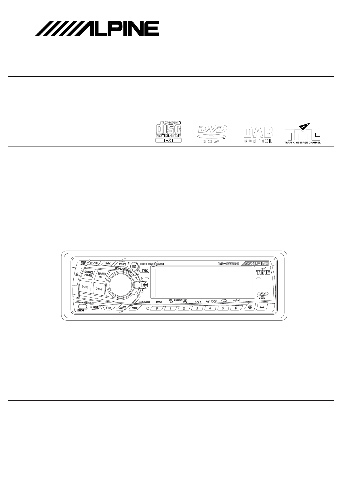
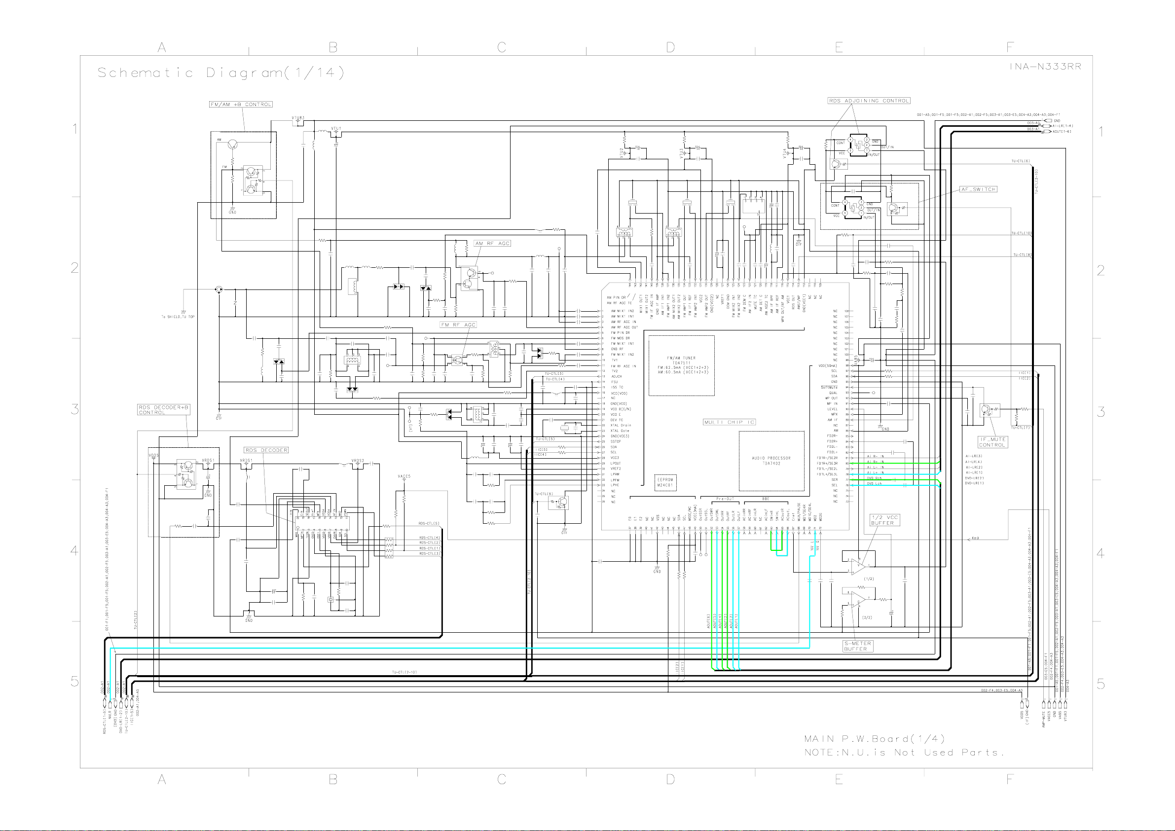
INA-N333RR
SERVICE MANUAL
GPS Car Navigation / CD Receiver
- Confidential -
10 /03-A
68E36039S01
"Schematic Diagram (ECU P.W.Board / ASSY,FPC SHEET SW) cannot use a reference function"
TO ALPINE Home Page
Page 2
<Cautions for Safe Repair Work>
r
s
.
- 2 -
The following cautions will prevent accidents in the workplace and will ensure safe products.
*The symbols indicate caution is needed to prevent injuries and damage to property.
The symbols and their meanings follow.
Warning
Caution
*The following symbols indicate two levels of cautions.
When you see this symbol, you have to be very careful.
When you see this symbol, you have to follow the instructions there.
If you ignore this symbol and handle the product incorrectly or unsafely,
serious injury or death may result.
If you ignore this symbol and handle the product incorrectly or unsafely,
injury or only material damage may result.
Warning
Do not look squarely into the laser light
coming from the pickup. Always use a designated fuse.
You may loose you sight. Use of an incorrect fuse may result in a fire.
Caution
Do not allow wiring to be caught in the Battery Caution
screw/chassis. Use the designated battery.
If wiring is caught in the screw/chassis, it may Confirm the correct polarity and seat of the battery.
cause a short circuit, resulting in a fire. An incorrect battery or an improperly connected or
Fuse Caution
seated battery may result in a fire.
High Temperature Caution Designated Parts Caution
Touching the heat sink may cause severe burns. Look up the part list and ensure that only
designated parts are used to prevent problems or
accidents.
Reverse Power Supply Connections o
Misconnections Caution Ensure that the wiring is correct when rewiring to
Reverse power supply connections or prevent problems with ignition/breakdown.
misconnections may cause ignition problems and
smoke may result.
Soldering Caution Wear Glove
Hot solder from solder splash may cause severe Wear gloves to prevent electrical shocks or injury
burns. from the end face of the metal.
For the FDA laser standard, the following CAUTION label is stuck on each product
Please be careful for repair.
CAUTION-Laser radiation when open, DO NOT STARE INTO BEAM
Wiring Caution
Page 3

Contents
- 3 -
INA-N333RR
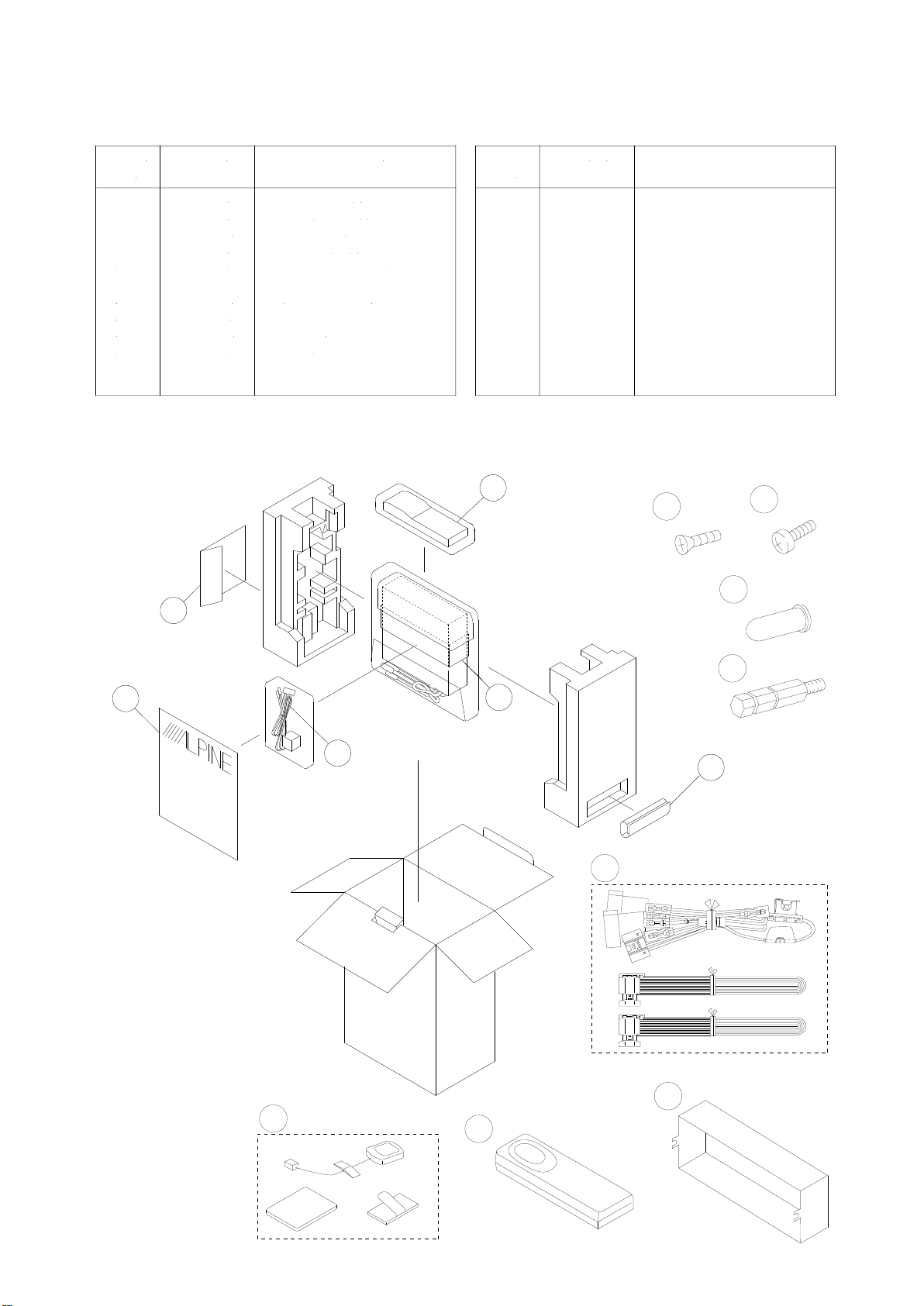
Packing Assembly Parts List
Packing Method View
System Connection
Specifications
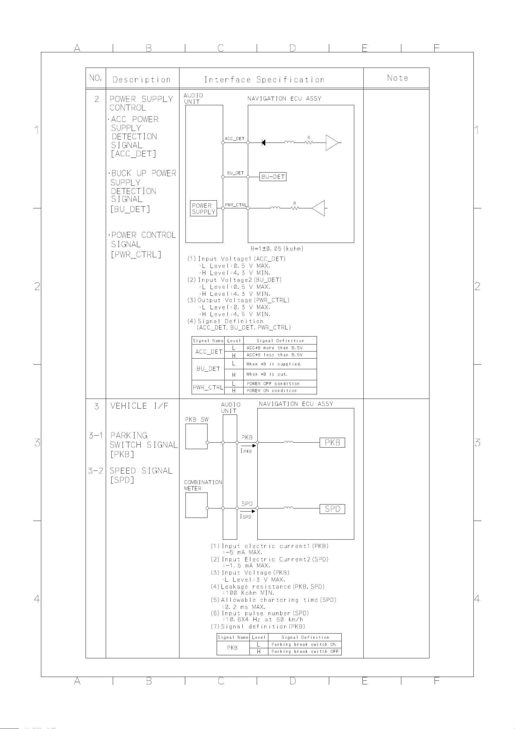
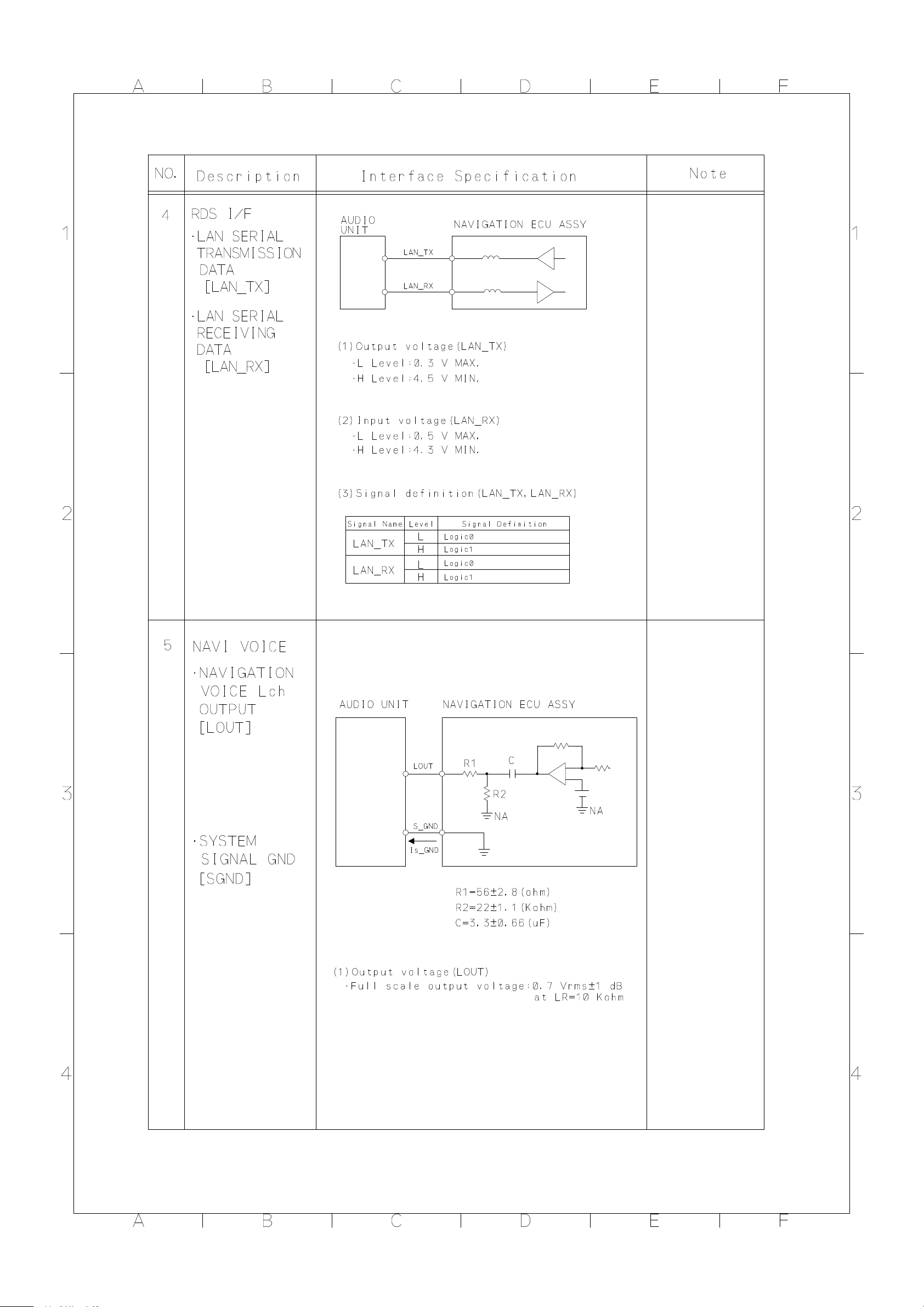
I/O Interface
5 to 7
8 , 9
10 to 16
Extension Cable
Adjustment Procedures
Block Diagram
Parts Layout on P.W.Boards and Wiring Diagram
Schematic Diagram
Terminal Voltage of IC/ TR
18 , 19
20, 21
22 to 26
27 to 40
41 to 48
4
4
17
Description of IC Terminal
Exploded View (Cabinet)
49 to 55
56 , 57
Exploded View (DVD Deck Mechanism) (DV33M010)
58
NOTE : Due to continuing product improvement, specifications and designs are subject to
change without notice.
Page 4
105
102
103
106
104
101
Packing Method View
101 -1
X4
105
X1
104
X1
101 -3
X1
101 -2
X1
101 -4
X1
X1
102
0.5
0.85
AMP
0.5
0.85
AMP
X3
X1
X1
103
Packing Assembly Parts List
Symbol
No.
Part No.
Description
101-1
101-2
101-3
101-4
102
103
104
105
106
03S60820Y16
03S60824Y01
36A11113W01
03A60836Y01
01T15359Y14
01T85385W04
15D50063Y01
15D50406W02
68P50520Y74
SCR,MCH 5X8 ZN A
SCR,WAV 1.7X4 ZN A
CAP,RUBBER(A)
SCR,CUS 5X7 ZN A
ASSY,ISO CONN N033RS
GPS ANT,GPA-CG2C1
CARRYING,CASE
CASE,INNER
O/M AOEU
Symbol
No.
Part No.
Description
INA-N333RR
- 4 -
TO CONTENTS
Page 5
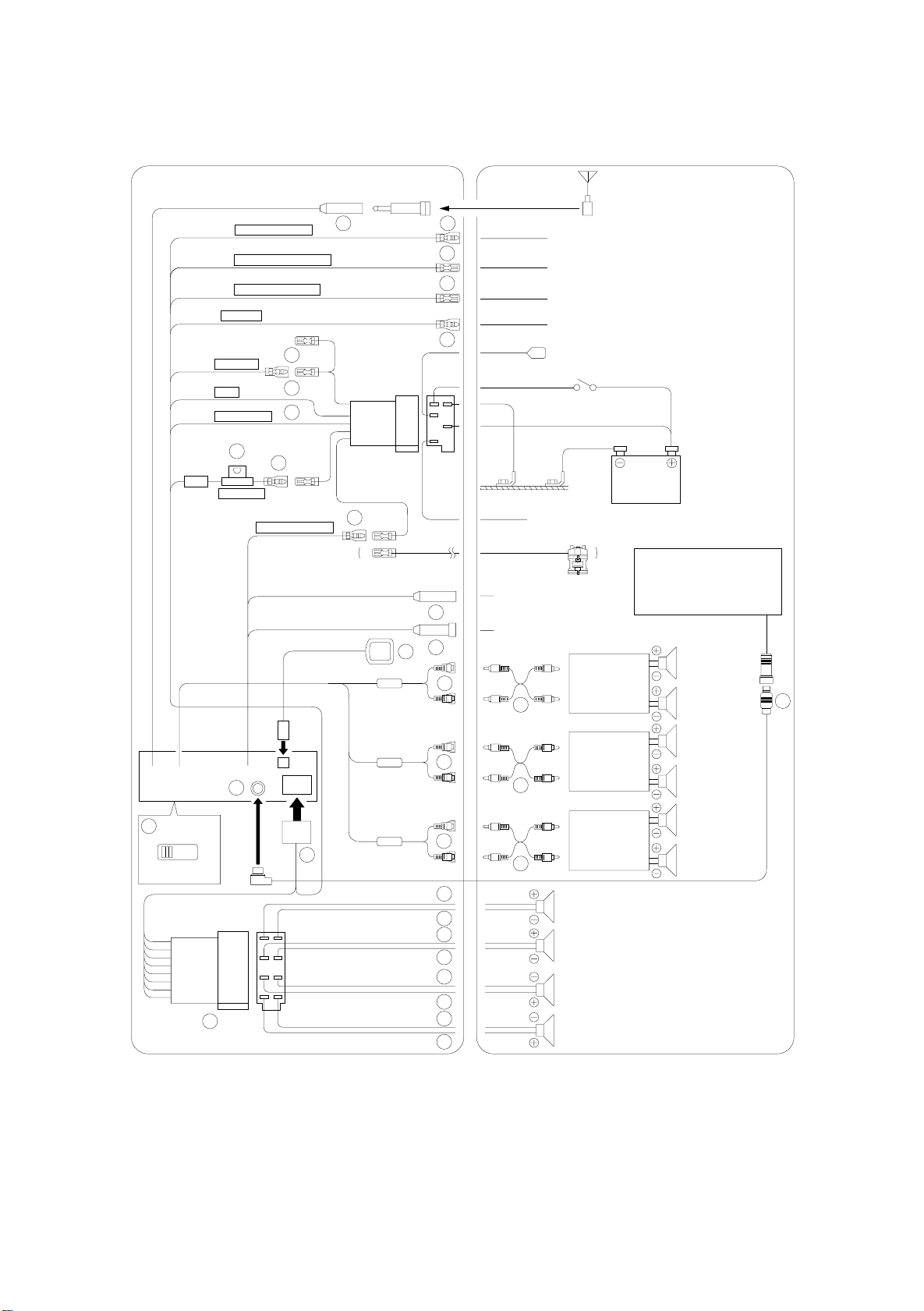
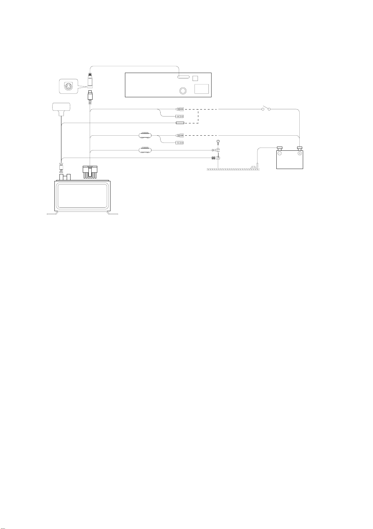
System Connection
- 5 -
TO CONTENTS
<Connection>
INA-N333RR
ISO Antenna Converter Plug
(Yellow/Blue) PARKING BRAKE
(Pink/Black) AUDIO INTERRUPT IN
(Blue/White) REMOTE TURN-ON
(Orange) DIMMER
(Red) IGNITION
(Black) GND
(Blue) POWER ANT
coil
10
BATTERY (Yellow)
choke
6
7
8
9
SPEED SENSOR
(Green/White)
1
12
*
speed sensor
auxiliary lead
Antenna
ISO Antenna Plug
2
3
4
5
To remote control
13
14
15
interface Box
To RDS-TMC Box (TMC-001P)
To the parking brake signal line
To vehicle phone
To amplifier or equalizer
To the instrument cluster
illumination lead
To power antenna
Ignition Key
Battery
To the vehicle speed pulse line
CD Changer
(Ai-NET)
(Sold Separately)
Speakers
18
Ai-NET
NORM EQ/DIV
24
19
22
20
17
21
16
(Green)
(Green/Black)
(White)
(White/Black)
(Gray/Black)
(Gray)
(Violet/Black)
(Violet)
-
25
26
27
28
29
30
31
32
22
22
Amplifier
Amplifier
Amplifier
Rear Left
Front Left
Speakers
Front Right
Rear Right
Front
Rear
Subwoofer
23
Page 6

INA-N333RR
- 6 -
TO CONTENTS
1
Antenna Receptacle
Connect to the supplied ISO antenna converter plug.
2
king Brak
Par
Connect this lead to the power supply side of the parking
brake switch to transmit the parking brake status signals to
the INA-N333RR.
3
Audio Interrupt In Lead (Pink/Blac
Connect this lead to the Audio Interface output of a cellular
phone which pro
received.
4
Remote Turn-On Lead (Blue/White)
Connect this lead to the remote turn-on lead of your
amplifier or signal processor.
5
Dimmer Lead (Or
This lead may be connected to the vehicle's instrument
cluster illumination lead. This will enable the vehicle's
dimmer control to dim the backlighting of the unit.
6
Switched Power
Connect this lead to an open terminal on the vehicle's fuse
box or another unused power source which provides (+) 12V
only when the ignition is turned on or in the accessory
position.
7
Ground Lead (Black)
Connect this lead to a good chassis gr
Mak
e sure the connection is made to bare metal and is
securely fastened using the sheet metal screw provided.
8
wer Antenna Lead (Blue)
Po
Connect this lead to the +B terminal of your po
if applicable.
e Lead (Yello
vides ground shorting w
ange)
Lead (Ignition) (Red)
w/Blue)
k)
hen a call is
ound on the v
wer antenna,
NOTE
This lead should be used only for controlling the vehicle's power
antenna. Do not use this lead to turn on an amplif
processor,
9
Batter
Connect this lead to the positive
battery.
10
Fuse Holder (10A)
11
ISO Power Supply Connector
Speed Sensor (Green/White)
12
Connect to
Improper connection of the speed pulse line may cause
important safety fe
brakes or air bags). Such failures may result in an accident
and loss of life. We strongly recommend that the installation
be performed by a tr
* If the connectors of the vehicle are not ISO type or they
etc.
w)
y Lead (Y
are ISO type but not equipped with the speed sensor
terminal on the v
supplied speed sensor auxiliary cable to connect to the
speed sensor cable of the vehicle.
ello
VSS (Digital or Analog 0V - 3V)
atures of the v
ained
ehicle side ISO connector
(+) post of the v
ehic
ized Alpine dealer.
, author
le to fail (suc
ier or a signal
ehicle's
, use the
ehic
h as the
le.
Remote Control Interf
13
To remote control interf
14
To RDS-TMC Receiv
ace Connector
ace box.
er (Optional)
NOTE
To connect an
dealer.
15
GPS Antenna (Included)
Power Supply Connector
16
Ai-NET Connector
17
Connect this to the output or input connector of other
product (CD chang
NET.
Ai-
System Switch
18
When connecting a pr
switch in the EQ/DIV position.
connected
Alpine RDS-TMC Recei
er
, Equalizer
ocessor using
, leave the
switch
in the NORM position.
consult your
ver,
.) equipped with
, etc
Ai-NET
When no de
Alpine
, place this
vice is
NOTE
Be sur
e to turn the power of
h position.
switc
Front Output RCA Connectors
19
RED is right and WHITE is left.
Rear Output RCA Connectors
20
-
RED is right and WHITE is left.
21
Subwoofer Output RCA Connectors
RED is right and WHITE is left.
22
RCA Extension Cab
23
Ai-NET Cable (Included with CD Changer)
24
ISO Connector (Speaker Output)
25
Left Rear (+) Speak
26
Left Rear (
27
Left Front (+) Speak
28
Left F
29
Right F
Right F
30
Right Rear (–) Speak
31
Right Rear (+) Speaker Output Lead (Violet)
32
–) Speaker Output Lead (Green/Black)
ront (–) Speaker Output Lead (White/Blac
ront (–) Speaker Output Lead (Gra
ront (+) Speak
f to the unit befor
le (Sold Separately)
er Output Lead (Green)
er Output Lead (White)
er Output Lead (Gra
er Output Lead (Violet/Blac
e c
y/Blac
y)
hang
ing the
k)
k)
k)
To prevent external noise from entering the audio system.
• Locate the unit and route the leads at
• Keep
• Connect the gr
• If you add an optional noise suppressor
suppressors, contact them for further information.
• Y
the battery power
ound lead securely to a bare metal spot (remove any paint, dirt or gr
our Alpine dealer knows best a
leads as far
least 10 cm away
away from other leads as possible.
, connect it as far away
bout noise prevention measures so consult your dealer for
from the car harness.
r
from the unit as possible.
ease if necessary) of the car c
hassis.
Alpine dealer carries various noise
Y
our
further information.
Page 7
<Connection with optional RDS-TMC Receiver Box TMC-001P>
- 7 -
TO CONTENTS
<INA-N333RR>
INA-N333RR
TMC-001P
Attached
antenna
ACC (Ignition) (Red)
Battery lead (Yellow)
Ground (Black)
TMC-001P
TMC Receiver Box
(Sold Separately)
For further information about the connection and
installation of TMC-001P, refer to the owner's manual of
TMC-001P.
NOTE
* Matching the optional Navig
to part of
the b
uilt-in
ation Disc (NVD-T003) with the RDS-TMC Receiver Bo
TMC tuner.
Ignition Key
Battery
x (TMC-001P) may cause function failure
Page 8

INA-N333RR
- 8 -
TO CONTENTS
Specifications
<FM RADIO>
Intermediate Frequency ......................................................................................................................... 10.7±0.1MHz
Frequency Range ............................................................................................................................... 87.5 to 108MHz
Usable Sensitivity (Mono, 30dB S/N, at 98.1MHz) .......................................................................................... 20.2dBf
-3dB Limiting Sensitivity (at 98.1MHz) ............................................................................................................ 21.2dBf
Residual Noise (Ref. 400Hz (narrow), at 98.1MHz) ...................................................................................... 28±10dB
S/N Ratio (at 98.1MHz) ......................................................................................................................... Stereo : 55dB
Mono : 58dB
Image Rejection (at 106.1MHz) .......................................................................................................................... 40dB
IF Rejection (at 90.1MHz) ................................................................................................................................... 60dB
Distortion (Input 60dBu, at 98.1MHz) ................................................................................................................... 1%
Frequency Response (Ref. 400Hz, at 98.1MHz) ................................................................................. 100Hz : 0±3dB
10kHz : -10±3dB
Stereo Separation (1kHz, at 98.1MHz) ............................................................................................................... 20dB
PS Sensitivity (at 98.1MHz) ............................................................................................................................ 36.2dBf
<MW RADIO>
Intermediate Frequency ....................................................................................................................... 1st. : 10.7MHz
2nd. : 450kHz
Frequency Range .............................................................................................................................. 531 to 1,602kHz
Usable Sensitivity (20dB S/N, at 999kHz) ........................................................................................................... 36dB
S/N Ratio (at 999kHz) ......................................................................................................................................... 44dB
Image Rejection (at 1,404kHz) ............................................................................................................................ 50dB
IF Rejection (at 603kHz) ..................................................................................................................................... 60dB
Distortion (at 999kHz) .......................................................................................................................................... 1.5%
Frequency Response (Ref. 400Hz, at 999kHz) .................................................................................. 100Hz : -3±4dB
2.5kHz : -5+3, -5dB
<LW RADIO>
Intermediate Frequency ....................................................................................................................... 1st. : 10.7MHz
2nd. : 450kHz
Frequency Range ................................................................................................................................. 153 to 281kHz
Usable Sensitivity (20dB S/N, at 216kHz) ........................................................................................................... 42dB
S/N Ratio (at 216kHz) ......................................................................................................................................... 44dB
Image Rejection (at 270kHz) ............................................................................................................................... 50dB
IF Rejection (at 162kHz) ..................................................................................................................................... 60dB
Distortion (at 216kHz) .......................................................................................................................................... 1.5%
Frequency Response (Ref. 400Hz, at 216kHz) .................................................................................. 100Hz : -3±4dB
2.5kHz : -5+3, -5dB
Page 9

INA-N333RR
- 9 -
TO CONTENTS
<CD SECTION>
System ....................................................................................................................... Optical (Compact Disc System)
Channel Balance (TCD-782, 1kHz) ................................................................................................................... 0±3dB
Distortion (TCD-782, 1kHz) ................................................................................................................................. 0.1%
Frequency Response (TCD-782, Ref. 997Hz) ....................................................................................... 17Hz : 0±3dB
127Hz : 0±2dB
10.007kHz : 0±2dB
19.997kHz : 0±4dB
S/N Ratio (TCD-782) ........................................................................................................................................... 80dB
Separation (TCD-782, 1kHz) ............................................................................................................................... 55dB
De-Emphasis (TCD-782, Ref. 1kHz) .................................................................................................. 4kHz : -20±3dB
16kHz : -20±3dB
<Pickup>
Wave Length .................................................................................................................................................... 655nm
Laser Power .................................................................................................................................................. CLASS II
<GENERAL>
Power Output (TCD-782 (Track No. 2, 1kHz), T.H.D. 10%) /Impedance .............................................. 18W/ch/4ohm
Pre Output (TCD-782 (0dB, 1kHz), Ref. FRONT, T.H.D. 1%) /Impedance ............................ 2V±2.5dBV/ch/10kohm
Sub-Woofer Output Level (TCD-782 (0dB, 1kHz), STEP-0, Ref. FRONT PRE-OUT) ................................... -15±3dB
Navigation Voice Output Level (1kHz, -6dB) ...................................................................................... 800±150mVrms
Back-Up Current .................................................................................................................................................. 5mA
Dimensions (W x H x D) ................................................................................................. Chassis : 178 x 50 x 158mm
Nose (at Closed) : 188 x 58 x 24.5mm
Nose (at Full Opened) : 188 x 58 x 52mm
Weight .................................................................................................................................................................... 2kg
NOTE : Due to Continuing product improvement, specifications and designs are subject to change without notice.
Page 10
INA-N333RR
- 10 -
TO CONTENTS
Page 11
INA-N333RR
- 11 -
TO CONTENTS
Page 12
INA-N333RR
- 12 -
TO CONTENTS
Page 13
INA-N333RR
- 13 -
TO CONTENTS
Page 14
INA-N333RR
- 14 -
TO CONTENTS
Page 15
INA-N333RR
- 15 -
TO CONTENTS
Page 16
INA-N333RR
- 16 -
TO CONTENTS
Page 17
INA-N333RR
- 17 -
TO CONTENTS
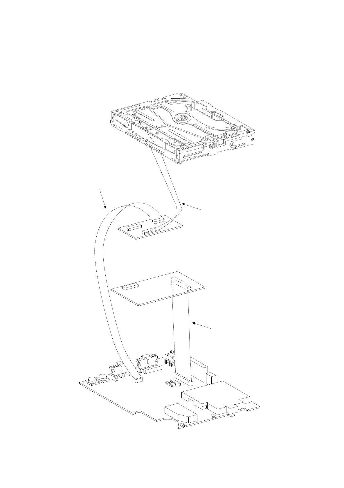
Extension Cable
* When repairing or measuring the voltage of this unit, connect with the Extension Cable as shown in below.
DVD Deck Mechanism
Extension Cable
(01E33127S01)
SUB P.W.Board
ASSY, NAVI CARD V-245
Extension Cable
(01E30083S01)
Extension Cable
(01V33125S01)
MAIN P.W.Board
Page 18
Step
Description
Connection
Signal Generator
Dial Control
Test Point /
P.W.Board
Coordinates
Adjustment
1
Signal Meter
Adjustment
Figure 2
90.1MHz, 26dBu
(Mod. OFF)
90.1MHz
TP503
(3-A)
TP504
(5-E)
Auto Adjustment :
After setting up of Signal Generator,
short GND and TP504.
(SPEC) TP503 : 1.5±0.1V
45ohm
10ohm
60ohm
Input
Output
For 50 ohm FM Signal Generator
Figure 1
FM Signal Generator
FM Dummy
Antenna
Antenna Receptacle
+
-
+
-
Unit Under Test
Figure 2
* only short-circuit at adjustment
TP503
GND
TP504
DC Volt Meter
Adjustment Procedures
- 18 -
TO CONTENTS
1. Tuner Adjustment
-1. FM SECTION
(1) Dummy Antenna Circuit
(2) Connection
INA-N333RR
(3) Control Settings
Fader Control ............................
Center Position Band Switch ............................................. FM
Balance Control ........................ Center Position Others .................................................... OFF
Treble Control ........................... Center Position
Bass Control ............................. Center Position
(4) Adjustment Procedures
Page 19
(4) Adjustment Procedures
Step
Description
Connection
Signal Generator
Dial Control
Test Point /
P.W.Board
Coordinates
Adjustment
1
MW
Signal Meter
Adjustment
Figure 4
999kHz, 30dBu
(Mod. OFF)
999kHz
TP503
(3-A)
TP504
(5-E)
Auto Adjustment :
After setting up of Signal Generator,
short GND and TP504.
(SPEC) TP503 : 1.0±0.1V
2
LW
Signal Meter
Adjustment
Figure 4
216kHz, 30dBu
(Mod. OFF)
216kHz
TP503
(3-A)
TP504
(5-E)
Auto Adjustment :
After setting up of Signal Generator,
short GND and TP504.
(SPEC) TP503 : 1.0±0.1V
For 50 ohm AM Signal Generator
15pF
30ohm
65pF
Input
Output
Figure 3
AM Signal Generator
AM Dummy
Antenna
Antenna Receptacle
+
-
+
-
Unit Under Test
Figure 4
* only short-circuit at adjustment
TP503
GND
TP504
DC Volt Meter
(2) Connection
(3) Control Settings
Fader Control ............................ Center Position Band Switch ..................................... MW/LW
Balance Control ........................ Center Position Others .................................................... OFF
Treble Control ........................... Center Position
Bass Control ............................. Center Position
-2. AM SECTION
(1) Dummy Antenna Circuit
NOTE : For the Test Points, refer to the Parts Layout on P.W.Boards and Wiring Diagram.
INA-N333RR
- 19 -
TO CONTENTS
Page 20
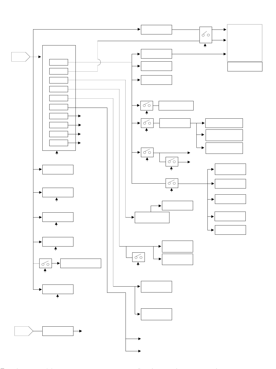
Block Diagram
- 20 -
TO CONTENTS
(signal Block)
INA-N333RR
FAN+B
TUNER
DVD MECHA
(DV33M010)
NAVI CARD
CONVERTER
MEMORY
JASO ANTENNA WIRE
IIC
ATAPI
3V-5V
FLASH
RESET
DIRECT ACCESS KEY
LED/LAMP
AUDIO
PROCESSOR
SERVO+5V SW
ADC
MCU
DISPLAY RESET
IS BUS
ROTARY
ENCODER
EJECT
ST MULTICHIP-IC
KEY MATRIX
EEP-ROM
IIC
MAIN u-COM
NAVI+3.3V
TAB II
NAVI u-COM
SERIAL BUS
DISPLAY
u-COM
OELD DISPLAY MODULE
AUDIO
BUFFER
Ai-NET Hi CIRCUIT
SYSTEM RESET/BATT-DET
REMO-CON
NAVI BUCK-UP+3.3V
D-RAM
SOUND CODEC
MEMORY-IC
I/R RECEIVER
POWER-IC
SERVO +7V
SWING MOTOR+B
OELD+B
VDD+5V/ACC+5V
NAVI +5V
TUNER+B
AUDIO+B
M
PREOUT-FRONT
PREOUT-REAR
PREOUT-SUB.W
4ch SP-OUT
TEL-MUTE CIRCUIT
ACC-DET CIRCUIT
SYSTEM
REGULATOR-IC
BATT-DET
5V-REG
5V-REG
8.3V-REG
8.5V-REG
7V-REG
HIGH-SIDE SW
PARKING BRAKE
CIRCUIT
SPEED SENSOR
I/F
GPS RECEIVER
GYRO SENSOR
REMO-CON DET
CIRCUIT
BATT
OREM+B
ST-REMO
Ai-NET
DIN
GT5
VEHICLE CONNECTOR (16P)
Page 21
(POWER SUPPLY Block)
- 21 -
TO CONTENTS
SYSTEM
BATT
REGULATOR-IC
BATT 5V
5V
*
7V
*
8.3V
8.5V
*
HSW
500mA MAX.
500mA MAX.
1.2A MAX.
150mA MAX.
250mA MAX.
1A MAX.
at usually 5V
power supply
3.3V REG
3.3V REG
MAIN u-COM
Ai-NET
RDS DECODER
Ope : 40mA MAX.
Erase : 100mA MAX.
19mA MAX.
NAVI-ON 5V
INA-N333RR
NAVI CARD
3.3V
1.2A MAX.
5V
500mA MAX.
3.3V BACK-UP
1mA MAX.
GPS RECEIVER
*
*
*
CD CHG
POWER-IC
AMP-ON
MOTOR+B
MOTOR-CNT
VHH+B
V-CNT
RESET
5.2V DET
4.5V DET
16V DET
IIC BUS
adjustable
*
EL-ON
1A MAX., 0.35A typ
150mA MAX.
MECHA SERVO+5V
MAIN u-COM
MAIN u-COM
NAVI u-COM
700mA MAX.
FM-ON
NOSE POWER
5.2V DET
MECHA SERVO
+7V REG
FM-ON
NOSE-ON+B
ACC
A-HOLD
FAN+B
80mA MAX.
1A MAX.
MULTICHIP
FMAM
MULTICHIP
7511
B-HOLD
A-HOLD
ACC-ON 5V
9mA MAX.
FM 62mA MAX.
AM 60mA MAX.
DISPLAY u-COM
GRAPHIC
MEMORY
REMO-CON
RECEIVER
MULTICHIP
EEP-ROM
ST-REMO
Ai-NET
IN-INT I/F
PARKING I/F
80mA MAX.
50mA MAX.
10mA MAX.
3mA MAX.
0.2mA MAX.
31mA MAX.
0.1mA MAX.
0.1mA MAX.
ACC 8.5V DET
LED+B
AMP-ON
270mA MAX.
MAIN u-COM
NAVI u-COM
MULTICHIP
7402 AUDIO
MECHA
AUDIO+B
P-ANT
500mA MIN.
O-REM
10mA
50mA MAX.
10mA MAX.
Page 22

Parts Layout on P.W.Boards and Wiring Diagram (1/5)
- 22 -
TO CONTENTS
MAIN P.W.Board
1
2
3
4
5
(Component Side View)
R097
R096
CB201
CB801
E263
R817
R829
R815
R819
C810
L882
L881
IC261
IC811
E262
CB271
E817
C882
C801
Q828
R827
E811
E815
E812
E814
E882
E881
C261
C263
C264
C262
D821
C816
IC881
C806
R826
R825
Q827
C818
R265
C267
C291
C294
Q826
E816
E813
Q841
ZD801
R618
Q261
C293
C292
R824
L884
R841
CB841
E264
R612
E823
R842
C618
Q842
R619
ZD618
R622
R621
C612
CB591
R617
L813
R292
CB583
CB611
E621
D611
C622
TP602
R573
R571
C655
Q611
D621
TP601
E701
R291
R578
ZD621
R611
Q622
Q621
C578
R579
Q625
D665
R658
C656
D581
D582
R657
Q562
R547
R574
L581
L582
R625
ZD665
C653
C652
C654
R659
C659
R562
C561
R575
R589
CB571
Q626
R654
C661
XL521
E861
R561
Q561
R587
Z581
Z582
R652
C523
R588
C651
D651
R653
R550
R861
C861
TP535
R549
R551
RA515
R576
R581
R582
R661
IC651
C522
TP501
R577
Q581
C581
R662
R656
RA521
R521
RA514
R539
IC581
R663
E651
R655
IC521
TP533
RA513
R563
R517
R518
R537
R536
Q627
E865
RA512
L865
C585
R590
SW201
R522
RA501
C503
XL502
C504
CB581
ZD521
ZD574
ZD573
E866
C867
RA511
R555
IC501
C866
R871
C874
R870
R515
R542
E867
R508
R543
R506
R507
C501
C502
E873
GR591
R073
R072
IC071
R063
R226
R222
C222
Q221
R224
R223
R221
C221
R225
R282R281
R262
IC282
IC281
C281
C506
R283
R264
RA509
XL501
IC871
LD631LD632
R552
C873
R284
R501
R878
E868
E871
RA508
C512
RA506
RA505 RA507
RA504
R263
TP505
E501
GS592
C225
Q062
R069
R261
R232
E872
L871
C029
C062
C063
Q002
R231
R251
R002
E061
E072
Q231
C232
R252
R241
R242
C605
C598
C224
C026
C231
C251
Q001
Q251
C252
C241
Q241
C242
TH641
C846
R849
Q631
C223
R062
L005
L001
R001
E001
C226
R061
R233
R234
R253
R254
R243
R244
C599
C064
R235
R236
R255
R256
R245
R246
R560
R559
R602
C590
C606
C027
C025
R298 R297R296 R293R295 R294
R603
C591
C023
L010
TP009
R605
C021
XL002
CB221
CB081
R606
R607
Q601
Q602
R601
C071
CF003
Q604
C601
C072
E011
R098
CB501
C603
Q603
D601
C602
IC001
CF002
R099
TP209
TP208
E012
E013
D891
Q899
R899
CB601
R032
C053
C898
Q853
VT005
CB891
ZD891
L853
E854
R1851
E006
E008
ZD898
R843
R844
R845
CF001
Q081
R1852
XL001
C036
C037
C052
C049
C048
C044
C046
VT004
R043
E007
E091
C891
C032
R019
IC891
VT003
VT002
R007
C077
E081
E853
D851
E852
C075
L091
E015
R012
C008
L007
C015
L006
C098
C099
C897
R891
C016
R092
C092
C009
C006
L092
R892
E014
Q003
C057
C076
Q004
E897
C078
D005
XL091
R893
VT001
C003
R010
R894
L852
R631
TP006
R895
INA-N333RR
ANT001
L002
L003
SW632
R632
R896
SW631
A
Orange Color Pattern:Component Side Pattern
Blue Color Pattern:Foil Side Pattern
BCDE FG
Page 23

Parts Layout on P.W.Boards and Wiring Diagram (2/5)
- 23 -
TO CONTENTS
MAIN P.W.Board (Foil Side View)
1
2
3
4
C002
L009
L004
SA001
R031
R006
C010
C001
D001
C050
C004
R091
R095
C096
TP002
R016
R015
C007
C012
C097
R897
R851
R855
L013
TP001
R024
R023
R037
C005
C013
D013
R009
R898
R852
R856
C054
D003
R017
C051
TP003
R005
D004
R011
TP004
C014
C894
R853
R857
C043
R029
R020
C087
IC091
C042
C035
TP005
R008
C011
R854
C040
C045
R004
C093
C853
R030
C017
R859
L854
C038
R018
C047
C083
Q898
R858
C041
D002
R021
C095
C091
R850
R1854
C030
R028
C039
C031
C034
C033
R050
IC087
C094
RA091
C852
IC851
Q1852
R1853
R013
L021
TP503
R886
R887
Q1851
C081
C055
R087
Q005
C082
Q852
R885
C856
F852
R035
L022
R022
C056
C018
C895
Q855
Q856
Q851
R036
C019
R044
C024
C058
R082
C066
Q897
C854
TP520
TP518
TP516
TP514
TP512
R026
C074
C020
C060
C061
Q006
R025
C065
R860
TP519
TP517
TP515
TP513
R846
R065
R074
TP061
C069
Q846
C073
R066
C028
R068
R064
C068
C022
TP511
R548
Q086
R086
IC086
R045
F846
R067
C594
R847
C086
C067
Q847
R831 R832
C593
R593
C555
R580
D871
R557
R584
R556
Q873
R504
R503
R641
R502
R553
R554
C556
R509
L504
C878
R880
C557
TP530
TP531
TP534
C505
L502
R879
Q872
R873
R075
R516
C509
L592
R534
Q628
C879
R513
R511
C507
C508
R875
C875
R872
L505
RA503
L501
C871
R874
R596
R505
R876
R877
C596
R595
R541
R519
L872
Q871
F865
C595
C597
R524
Q521
RA510
TP502
D501
RA502
R520
R525
R512
R538
C511
Q865
R531
R526
R514
L597
R530
R527
R533
R535
TP532
L503
R510
R866
R868
R867
C532
Q623
R528
R544
R545
R546
R865
R529
C521
R532
C510
R540
C530
L595
R623
Q624
R838
R839
R837
L596
L521
C524
C531
R624
R651
C657
R523
Q861
TP597
R833
R634
R583
C658
D521
R615
TP504
Q866
R863
R862
Q862
R834
R633
C865
C864
IC864
D864
R835
R836
TP571
TP594
R572
TP593
TP591
TP595
TP596
TP592
Q262
Q263
D826
R616
Q615
C616
R823
R822
R821
R806
C883
R820
R807
R830
R884
L883
Q825
R818
R811
C814
Q811
R882
R883
R808
C811
R816
C815
C822
C821
R812
C807
C265
R805
C813C812
C881
C817
D881
Q881
R881
D801
R266
R828
C803
C819
R802
R801
C802
C804
INA-N333RR
C805
5
A
Orange Color Pattern:Component Side Pattern
Blue Color Pattern:Foil Side Pattern
BCDE FG
Page 24

Parts Layout on P.W.Boards and Wiring Diagram (3/5)
- 24 -
TO CONTENTS
INA-N333RR
1
2
3
LD921
SW909
SW913
LD927
LD911
SW907
LD922
IC909 IC910
LD925LD926
PL901
C958
C957
FRONT P.W.Board (Component Side View)
SW904
LD904
LD913
SW905
LD909
LD906
SW901
LD902LD903
SW90
2
907
LD
R1078
LD914
LD908
R1066
LD901
SW906
SW914
R1098
R1099
R1100
R1101
R908
R909
R910
R903
R930
R1075
R929
R1074
R915
R1076
C911
R968
R969
R970
R971
R914
D904
R906
R1043
R1044
R1084
R1086
R905
R1002
R1087
R1085
D905
R1097
R1010
R902
R907
R1096
R966
R1004
R1082
R972
R967
C912
R1012
C904
R991
R1094
R1081
R1006
C918
R1089
C917
R1088
R1095
C909
R977
R1014
R1083
R916
D906
R1093
C921
R918
R1106
R913
LD910
SW903
SW908
LD924
LD905
LD923
SW910
SW911 SW912
LD912
FRONT P.W.Board (Foil Side View)
C955
C956
C915
C916
IC902
R911
C923
Z901
IC912
C924
R1080
TP984
C925
TP983
C926
C927
TP965
TP977
TP976
TP975
TP985
R925
R1055
RA906
RA910
C950
Z903
R1065
XL901
C901C902
RA905
R1048
R1049
R1047
R1113
R1069
R1068
R1070
R1071
R1072
R1112
R1008
R1111
R1007
CB902
TP994TP992
TP993TP991TP988
IC901
TP995
R1110
L902
R900
R932
Q908
CB905
Q907
R931
Q991
C922
R1041 R1042
C992
IC991
CB904
R901
C905 C907
C991
ZD902
ZD903
R1090
C919
Q906
R1045
R1046
Z902
L901
Q905
C951
C952
C953
C954
CB901
RA909
RA903RA902
RA908
RA907
R1000
R998
R1077
R999
R973
R997
R974
IC911
R990
Q902
Q901
Q909
R1116
C910
R1001
RA904
R992
R1104
R980
R988
R986
R983
R917
R919
R1003
R1115
R1114
R1036
Q904
Q903
R981
R984
R1034
R982
TH901
R994
R1031
R1030
R927
R1032
R1035
R1033
R1029
RA901
R993
R996
R1027
R1024
R1028
R1026
R1118
R1022
R1025
4
5
A
Orange Color Pattern:Component Side Pattern
Blue Color Pattern:Foil Side Pattern
BCDE FG
Page 25

Parts Layout on P.W.Boards and Wiring Diagram (4/5)
- 25 -
TO CONTENTS
1
INA-N333RR
AMP P.W.Board
(Component Side View)
2
3
AMP P.W.Board
(Foil Side View)
4
5
R715
R716
CB701
CB702
R703
C705
C706
C707
R709
R712
R708
R711
R713
IC702
R714
TP702
R710
R704
R706
R705
L705
R702
L702
L703
L704
R701
L701
TP701
C701
C702
C703
CB703
IC101
A
SUB P.W.Board
(Component Side View)
Orange Color Pattern:Component Side Pattern
Blue Color Pattern:Foil Side Pattern
BCDE FG
Page 26

Parts Layout on P.W.Boards and Wiring Diagram (5/5)
- 26 -
TO CONTENTS
1
INA-N333RR
2
FPC,DRIVE P.W.Board
(Foil Side View)
LIMIT P.W.Board
3
(Foil Side View)
4
FPC,LOAD P.W.Board
(Foil Side View)
TP418
TP417
SW406
MAIN-LSI P.W.Board
(Foil Side View)
TP104
TP103
TP105
TP444
TP101
TP409
R440
TP202
SD402
TP405
TP406
TP441
TP411
TP412
TP416
TP415
TP413
R360
TP414
TP355
TP356
CB601
TP357
TP358
TP369
TP400
TP430
TP429
TP344
CB60
TP390
TP337
TP339
R518
TP383
C526
TP316
R517
Q507
C525
Q508
TP308
E505
TP440
TP102
R631
R345
C301
TP410
TP204
R630
E301
TP367 TP368
TP359
TP338
2
TP385
TP388
E503
C524
TP317
TP107
R131
R102
C361
C302C303
TP360
TP439
R403
C451
C450
TP401
C512
C513
C529
C530
C507
C523
R520
TP112
TP113
TP106
C362
R308
R302
C318
TP207
TP442
R415
C401
TP402
TP320
R519
TP307
TP111
TP109
C358
TP246
R304
R303
TP313
R325
R323
C403
C402
R426
CL401
R402
TP325
TP321
TP327
IC501
TP110
RA101
TP108
RA102
C317
C307
TP247
C346
R324
SD602
R428
TP326
L301
TP324
TP387
C308
R329
R332
TP312
R439
C808
TP404
TP386
R504
CB101
RA103
R331
TP364
TP457
C415
C453
C452
C809
R808
R809
TP391
TP381
TP403
TP382
TP384
R505
R503
C501
RA104
IC301
TP288
C406
C454
R425
TP447
C506
C503C504
R506
R507
C502
R524
RA105
R305
C322
IC401
TP262TP263
TP279
R513
C511
R509
R508
TP318
TP319
C505
C804
R804
R807
C807
C314
R306
XL301
TP363
TP393
C404
R422
TP264TP265
R514
R515
C510
Q501
TP322
C806
RA106
C354
TP394
R407
R406
TP282
TP456
TH402
TP453
R806
R307
TP335
R340
R418
TP323
TP212TP213TP216
TP214TP215
TP219
TP220
TP139
TP138
TP141
TP140
TP285
R122
R322
C334
C333
C328
C330
R330
C712
R328
TP445
C604
R437
C419
C410
R442
C420
R443
C405
R417
TH401
TP218
TP222
TP221
TP223
TP142
TP289
TP306
TP284
TP304TP305
R318
C364
R316
C329
C320
C319
R333
C321
TP273
TP446
C418
IC403
C411
TP267
R423
C416
R424
R404
C408
IC402
R409
TP443
CB401
TP224
TP144TP145
TP143
TP353
TP302TP303
TP301
TP294TP295
TP296
TP293
TP292
TP354
C348
TP274
C417
TP351
R416
R405
TP352
MAIN-LSI P.W.Board
(Component Side View)
R121
SW403
C352
C357
C353
R313
R334
C606
R603
R604
R419
SW404
R124
R352
R413
C351
R311
C347
C345
R450
R132
R309
R312
C356
C810
R810
C811
R126
R133
C339
C340
C338
C337
C311
C310
TP291
C355
R614
R811
R414
R451
R128
R129
R125
R127
R421
C335
R310
TP449
R643
R611
R123
R118
R119
RA107 RA108
C313
R321
C312
R317
R702
R642
R640
IC601
R533
R320
R319
C332
C360
R646
R645
R644
R647
R615
R641
C802
C803
C331
E702
C309
R351
R408
R802
R101
C101
C336
C704 C705
TP448
R338
R337
TP450
TP451
C365
C363
R803
R705R706
C702C703
R339
R336
R601
R639
R636
R635
R638
R637
R427
R410
C516
R510
R120
C359
R707R708
R717R718
C706
TP210
IC701
R350
TP452
SD603
R438
C407
C521
C519
C518
C315
C316
C812
R801
IC201
R203
C202
R206
C203
IC202
R512
C515
C514
C813
C801
E202
E203
R511
SW401
IC203
R813R812
C800
SW402
R209
R800
RA109
R357
R356
R355
R301
C304
R522
R521
R544
R528
R530
C528
R529
R531
SW405
R411
R412
RA110
R212
C305
C205
R545
R200
R722
R723
R208
C207
R204
R210
C204
C522
IC204
Q506
R724
R725
R726
5
A
Orange Color Pattern:Component Side Pattern
Blue Color Pattern:Foil Side Pattern
BCDE FG
Page 27
XN1A312
- 27 -
TO CONTENTS
TO PARTS LIST
TO P. W. BOARD
R082
22k
Q081
C082
1u
Q001
2SA1774
R001
R002
ANT001
ASSY,ANT 033RO/561A0
SA001
E081
10/16
100p
C083
2200p
C093
330p
C094
3.3k
1.5k
CSA30-201M
C092
Q002
XN1A311
C002
0.022
L001
2.2uH
E006
4.7
R044
E001
L005
22/16
2.2uH
C026
0 . 022
R021
L021
L007
68uH
68p
D002
KV1410
C016
R013
56k
R019 3.3k
C081
0.047
L022
BK1608HM102
XL001
10.25MHz
R025 1k
R026 1k
N.U.
C058
100p
C031
0.022
TP005
10
C017
C044 0.022
C045 0.022
C046 0.022
C048 6p
C049 6p
C052 10p
C033
0.01
Q006
1
C077
3300p
0.1
C034
N.U.
C030
N.U.
C029
N.U.
R022
C036
BK1608HM102
C015
R011
4.7k
0.01
C013
C076
7p
C047
100
56k
R018
10
1p
68p
C035
C032
15p
C037
22p
0.1
N.U.
E015
C039
22/16
R004
22
1k
1mH
R008
4700p
TP002
22k
10k
L006
1M
R010
C051
OSC F/A 5KR
TP004
Q004
FC18
1
VT002
RF FM 5KR
R012
10
0.01
R017
VT003
E014
C038
22/16
L013
2.2uH
C041
C040
2200p
0.01
R028
100k
C043
C042
0.01
1000p
R029
56k
R030
5.6k
2.2k
R007
R009
2.2k
1
C075
C014
1000p
Q003
3SK195
1
0.01
C050
C078
D003
R023
0.01
5.6k
KV1410
680
R024
0.1
C011
10p
C003
0
R031
D005
1SV316
L009
0.22uH
L091
BK1608HM102
E091
2.2/35
C091
0.022
1000p
0.01
C057
C095
560p
IC091 SAA6588T
470k
R091
C004 7p
C005
C097 2200p
C037
11p
C087
BK1608HM102
XL091
4 .33MHZ
56k
N.U.
L092
R092
L002
4.7uH
L003
C006 1p
VT001
ANT1 FM 5KR
D004
C098
27p
5.6k
C099
27p
L004
R006
15uH
10-1/4
52mH
C008
N.U.
5p
C007
R020
KV1410
56k
C096
0.022
C009
TP003
R095
1k
RA091
8p
1kX4
R005
D001
MA133
22
R098
C001
0.022
C012
D013
1SV172
R015
0.01
C010
R016
C054
TP006 TP001
10k
R099
10k
22/16
C018
N.U.
CF 001
SFELA10M7
12k
VT004
IFT1 F/A 5PG
R050
C055 100p
R032
E007
4.7
R043
22/16
C019
N.U.
XL002
CFWLA450K
CF003
CF002
SFELA10M7
SFELA10M7
VT005
IFT2 AM 5PG
C056 0.022
220-1/4
TP209
TP208
C053
0.022
R035 470
R036 470
E008 22/16
C020 0.1
IC001
TDA7518
TP009
C021 0.022
C060 0.47
E011 10/16
C061 0.47
C022 3900p
E013
10
R045
N.U.
10k
R087
C025
0.01
C024 0.01
E012 22/16
1mH
120p
0.1
L010
C027
C023
R074
100k
1
10u
C071
C5911C590
R073
C074
Q005
UN9215J
C086
0.1
0.1
1k
C073
R065
NJM2904V
R072
1K
NJM2904V
TC7S66F
IC086
TC7S66F
0.22
0
E061
22/16
TP061
IC071
IC071
IC087
N.U.
C066
R064
N.U.
C067
C064
1000p
C605 N.U.
C598
1
R075
2.2K
C028
0.1
R068
220k
C065
0.015
47p
C068
N.U.
C069
R061
470
R062
470
E072
10k
R086
Q086
UN9212J
R067
0.22
C606 N.U.
C599
1
C072
10/16
4.7k
R066
0
0.1
Q062
C063
UN9212J
0.68
C062
10u
R063
R069
N.U.
0
Page 28

CB591
- 28 -
TO CONTENTS
TO PARTS LIST
TO P. W. BOARD
FH12-20S
C593
TP591
TP592
TP593
TP594
TP595
TP596
TP597
0.01
ASSY,DIN BVN033R0
100k
R593
ET583-2
GS592
53253-0310
0.01
C594
CB583
D581
MA133
D582
MA133
C555
BLM18PG300SH1
22
22
C556
TP502
R543
CB081
R559
N.U.
1k
Z581
CKD510JB1H221S
Q581
R581
UN9211J
100-1/4
L581
RA512
R535
N.U.
R533
L503
BK1608HM102
R544
10k
10k
R540
R563
C510
R510
1k x 4
R545
22k
N.U.
0.01
R583
BLM18AG102SH1
2.2k-1/4
L582
L592
R582
Z582
10k-1/4
BLM18AG102SH1
CKD510JB1H221S
22
C557
IC581
TC7WH14FK
0.01
C581
C530
4.7
L595
BLM18PG300SH1
C595
0.01
C596
0.01
L596
BLM18AG102SH1
R595 100
C531
GR591
4.7
R596
L597
BLM18PG300SH1
4.7
0.01
C532
C597
100
CB501
BM(10)B-SRSS
TP512
TP515
TP513
TP514
TP511
47k
R549
47k
R551
TP516
TP517
TP519
TP518
TP520
R560
1k
47k
R548
R538
100
TP532
D501
R509
MA113
0
TP533
C511
0.01
RA513
1k x 4
RA514
1k x 4
TP535
R532 1k
N.U.
R546
R517 470
R518 470
R537 1k
R536 1k
0
RA515
1k X 4
1k
47k
1k x4
RA511
R534
470-1/4
N.U.
R555
1k x4
RA510
IC501
D70F3032BGF
R515
R542 1k
1k x4
RA509
R508 47k
R507
47k
R506
1k
47k
C506
BK1608HM102
TP531
TP530
TP534
0.022
R512
0
R511
47k
R516
270p
L505
C512
C505
N.U.
N.U.
R514
R513
RA508
0.01
R505
47k L504
BK1608HM102
TP503
RA507
1k x 4
RA506
1k x 4
C509
0.01
R501
1k
0
1k x 4
RA504
1k x 4
R556
0
Q628
XN1A312
R504
47k
R503
470k
TP505
R502
47k
RA505
1k x 4
L502
BK1608HM102
R557
0
R552
1k
22k
TH641
R641
8.2kF
22k
22k
R539
R520
TP501
R554
100
160-1/4
R527
TP504
R524
160-1/4
R525
160-1/4
R526
160-1/4
Q604
UN9211J
1500p
2.2k
R528
1.5k
R530
22k
R606
R607
1k
1.5k
R529
2.2k
R531
C603
1000p
CH571
ASSY, UNIZON CONN 33N
R553
100
D521
CB581
TWK-E80P-E1
47k
R655
10k
C657
470p
R624
Q624
UN9212J
E651
22/16
R654
10p
220k
R659
C659
NJM3404AV
10u
R653
C661
R661
47kF
Q627
UN9212J
R656
120k
100k
R584
R590
100
100p
C585
100k
R580
0.1
10u
C652
C651
IC651
10k
R663
R662
100kF
47k
R623
Q623
UN9212J
D651
MA133
C656
10k
10kF
R652
10u
C654
10kF
R651
10k
10u
C658
R657
47k-1/4
R658
10k-1/4
0.01
C653
1000p
ET583-1
ASSY, DIN BVNO33R0
XL521
4.00MHz
27p
C522
53253-0310
CB601
RA521
4.7k x 4
C523
R550
3.3k
27p
IC521
100p
MB88385CPF
C524
C521
0.022
4.7k
R521
R602
3.3k
R603
2.2k
C601
100-1/4
0.1
C601
R522
Q601
2SA1774
Q602
UN9212J
4.7k
1SS355
L521
ZD574 RLZ7.5A
22k
Q603
UN9211J
BLM21PG221SH1
D601
MA132WK
Q521
UN9111J
C602
R523
10-1/4
ZD521
MAZS0560L
ZD573 RLZ7.5A
R605
C503
RA501
XL502
32.7kHz
10p
R573
22K
CB571
1
L501
C507
1k x 4
10p
C504
10k
R571
52271-1590
C508
XL501
19.9MHz
8p
15p
C501
C502
R574 1k
R572 0-1/4
R578 1k
R579 1k
1k x 4
BK1608HM102
RA502
0.01
R575 1k
R589 1k
R587 1k
R588 1k
R576 1k
R577 1k
R541 47k
R519 47k
1k x 4
RA503
E501
100/16
R547
10k
Q562
2SB1132
22k
N.U.
C578
TP571
Q561
UN9212J
0.01
C561
R562
1.5k
R561
Page 29

C223
- 29 -
TO CONTENTS
TO PARTS LIST
TO P. W. BOARD
C224
R221
220
R222
R231
R232
R241
C242
1u
1u
220
220
220
R251
R252
220
220
220
SW201
SLD-42-508X
C225
1u
C226
1u
R225
Q231
Q251
Q241
100
22k
R223
22k
R224
R226
100
R235
100
22k
R233
22k
R234
R236
100
R255
100
22k
R253
22k
R254
R256
100
R245
100
22k
R243
22k
R244
C246
100
C224
Q221
2.2u
C222
XN0F256
2.2u
C231
2.2u
C235
XN0F256
2.2u
220
C251
2.2u
C252
XN0F256
2.2u
C241
2.2u
C242
XN0F256
2.2u
R297
R298
R292
0
R291
0
CB201
CON, TCP 9389-11
CB221
R297
53253-0910
0
0
0
R294
R295
R296
0
0
0
ET221
ASSY, WIRE RCA NO33RO
R261
120
IC281
NJM4580V
R263
120
R262
120
NJM4580V
R264
120
C281
R283
R282
IC282
NJM4580V
IC282
R284
R281
1.1k
NJM4580V
1.1k
1.1k
1.1k
1
IC281
Q263
UN9112J
Q262
UN9212J
C294
C293
C292
C291
UN9212J
1
1
1
1
Q261
C263
0.33
C264
0.33
0.33
C262
0.33
C261
R265
10k
E263
4700/16
R266
820k
CB271
0.47
C267
E262
100/16
E264
10/16
C265
0.01
IC261
TA8270H
IMSA9210B-1-10Z
Page 30

C861
- 30 -
TO CONTENTS
TO PARTS LIST
TO P. W. BOARD
0.022
D864
RB161M-20
L883
E881
N.U.
C883
E861
C865
BLM21PG221SH1
470/16.
R861
100/16
Q862
UN9211J
S-817A33ANB-T2
10u
R883
3.9k
N.U.
R884
C881
0.022
N.U.
IC864
Q861
2SB1188
L881
220uH
R882
22k
R863
R862
330-1/4
R851
R854
N.U.
1.8-1/4
R852
R855
1.8k-1/4
R856
1.8k-1/4
R857
1.8k-1/4
R860
Q855 N.U.
1.8-1/4
R853
1.8-1/4
IC851
C854
1500p
470-1/4
MC34063AML
R858
33kF
L853
1000uH
E853
0.01
C853
470/16
E856
R859
2.2kF
390
R885
100
R887
1k
R886
Q852
2SA1797
2A
F852
R844
0.01
1.5k-1/4
Q853
UN9211J
L852
RB050L-40
N.U.
330/25
1.5k-1/4
Q1852
UN9212J
D851
0.01
C852
Q851 2SC4672
Q856 N.U.
1500uH
E852
330/25
L854
BLM21PG221SH1
10u
C864
IC881
LM2576S
47k
R881
L882
100uH
D881
E882
1.2k
100/16
Q881
0.01
RB050L-40
C882
UN9212J
R850
E854
R1853
1k
Q1851
2SB1132
R1854
R1852 180-1/4
R1851
180-1/4
MOTOR , F3010CU-12UCV
R843
24k-1/4
R845
1.5k-1/4
DTC124EKA
10/16
R823
Q827
E823
M841
2SA1037AK
10k
Q825
R822
53253-0210
2.2k-1/4
CB841
R821
Q841
2SB1198K
22k
R841
1.5k
R842
Q842
UN9212J
R818
R805
8.2-1/4
R806
8.2-1/4
R807
10k-1/4
8.2-1/4
R808
8.2-1/4
R820
10k
2SB1243
10k
R824
R825
1.8k-1/4
D826
1PS226
Q828
DTC143EKA
R826
R826
1.8k-1/4
R827 10k-1/4
D821 MPG06G
E811
C811
0.022
100/16
L813
10uH
E812
100/16
100/16
E813
C812 0.022
C813 0.022
220kF
R816
22k
100/16
E815
E813
C814 0.022
100/16
L884
10uH
R811
220kF
R812
180kF
1
N.U.
C821
C822
E817
E816
C815 0.022
100/16
100/16
C816 0.022
C817 0.022
TP602
R815
220k-1/4F
0.1
C818
E701
470/10
IC811
L5952
R819
C819
1
0.01
C810
470
R829
470
R817
68kF
TP601
Q811
XN1A312
22k
R828
R830
47k
R633
470-1/4
R634
560-1/4
SML-010DTT87
R631
47k
R632
47k
Q611
UN911LJ
47k
R611
SML-010DTT87
LD631
SW631
SPVG13
SW632
SPVG23
MA132WK
LD632
Q631
UN921FJ
D611
D891
MA4S159
R612
10k-1/4
C612
0.022
M891
MOTOR , LOAD FF-050SK
C891
0.022
R617
ZD618
R619 220k
CH891
ASSY , CONN 2P
ZD891
MAZS0430H
R618
22K
1k-1/4
0.01
C618
MAZS0510H
IC891
BA6219BFP
R891
33-1/4
CH891
53253-0210
R892 33-1/4
R893
33-1/4
Q873
2SJ327
L871
C895
0.022
Q897
2SD1760
R897
2.2-1/4
Q898
2SD1760
R898
33-1/4
33-1/4
33-1/4
R895
R896
R894
47k
R615
Q615
UN9212J
2.2-1/4
C897
0.022
C894
0.022
E897 100/16
R616
10k-1/4
1u
R616
ZD898
C898 1
R899
390-1/4
MA1Z120
Q899
XN1A312
100uH
Q872
C879
D871
RB050L-40
L872
BLM21PG221SH1
E871
E873
C871
E872
100/16
0.022
100/16
100/16
Q622 UMC2N Q621 UMC2N
10u
C622
FMY1A
1000p
C878
0.047
R880
100-1/4
R879
10-1/4
Q871
UN9211J
R874
22kF
R878
1.2kF
R875
22kF
270F
R877
220F
R876
IC871
TL5001
C874
10u
C873
R873
0.1
C875
R872
R871
100k
0.1
22kF
R870
D621
1SS355
470-1/4
470-1/4
C867
ZD621
MAZS0680H
E621
L865
100uH
0.01
E868
E867
100/16
R621
4.7k-1/4
R622
0.1/50
Q865
2SA1797
F865
2A
R866
R837
E866
E865
100/16
100/16
4.7k-1/4
820-1/4
820-1/4
Q866
UN921LJ
100/16
R867
820-1/4
R838
820-1/4
0.01
C866
Q625 XN1A312
R865
24k-1/4
R835
R836
1.8-1/4
R868
820-1/4
R839
820-1/4
1.8-1/4
R834
R833
1.8-1/4
1.8-1/4
R831
R832
1.8-1/4
1.8-1/4
Q846
F846
2SA1797
2A
R846
24k-1/4
C846
0.022
R847
UN9211J
Q626
UN9212J
Q847
R625
10k
1.5k-1/4
D665
SC25-02WS
S1G-6904
N.U.
C655
2200p
ZD665
R849 N.U.
CB611
C805
0.01
C804
0.01
0.01
C801
C806
0.01
ZD801
ZSH5MA27A
0.01
C803
0.01
C802
ET583-3
ASSY,DIN BVN033RO
D801
S1G-6904
R802
270-1/4
R801
270-1/4
CB801
CON,53377-16220
0.01
C807
Page 31

R1115
- 31 -
TO CONTENTS
TO PARTS LIST
TO P. W. BOARD
68
OELD901
OELD,UEL10010
22k
IC991
S-80935CLMC-T2
22k
R991
CB902
FH12-30S-0.5S
TP995
TP988
C905
0.022
C907
0.022
CB904
FH12-30S-0.5S
R1081 100
R1082 100
R1083 1k
R1084 1k
R1085 1k
R1086 1k
R1087 1k
SW902
ENC , EC11E0B2LB
R1024
R1022
2.2k-1/4
2.2k-1/4
LD926
LD923
AA1111C
AA1111C
LD925
LD922
AA1111C
AA1111C
LD924
LD921
AA1111C
AA1111C
Q901
R1026
1.2k-1/4
2SD1328
1k-1/4
R1025
LD927
SML-511DW
R982
R981
R1032 150-1/4
R1034 150-1/4
R1036 150-1/4
R1035 150-1/4
R1033 150-1/4
R1031 150-1/4
LD901
PL901
BRBG1211C
6V-80mA
Q903
R980
820
UMC3N
R1045 10k
R986
R984
820-1/4
3.3k-1/4
270-1/4
R983
1k-1/4
330-1/4
LD902
BRBG1211C
R1048 10k
R1046 10k
R1047 10k
R988
R990
R992
1.2k-1/4
3.3k-1/4
1.2k-1/4
LD906
LD909
BRBG1211C
BRBG1211C
LD905
LD908
BRBG1211C
BRBG1211C
LD904
LD907
BRBG1211C
BRBG1211C
R1104
Q904
680
2SD1328
UMC3N
R1110 68
TP991
TP992
TP993
TP994
R1049 10k
R996
R994
R998
1k-1/4
270-1/4
1.8k-1/4
R997
R993
R1118
1k-1/4
330-1/4
1.5k-1/4
LD911
BRBG1211C
LD910
BRBG1211C
Q902
R1113 68
R1114 68
68x4
R1112 68
R1111 68
RA907
68x4
RA908
68x4
RA909
68x4
R1095 100k
R1000
R1028
470-1/4
R999
R1027
470-1/4
LD914
BRBG1211C
LD913
BRBG1211C
RA910
68x4
RA906
R901 68
R972 1k
R966 1k
R967 1k
R968 1k
R969 1k
R970 1k
R971 1k
R1096 100k
R1098 100k
R1100 100k
R1097 100k
R1099 100k
R1101 100k
R1007 1k
R1008 1k
R1068 1k
R1069 1k
R1070 1k
R1071 1k
R1072 1k
R1030
1.2k-1/4
270-1/4
R1029
330-1/4
1.5k-1/4
LD912
BRBG1211C
LD903
BRBG1211C
SW901
SW903
Q991
UN9212J
RA905
R902
10k
SW911
68x4
C901
10p-CH
C951
0.022
68x4
RA904
IC901
M30803FGGP
XL901
20.00MHz
C902 8p-CH
10
C952
C953 10
SW904 SW905
SW908SW907
SW912 SW913
N.U.
C992
C954
C991
0.022
68x4
68x4
RA903
RA902
L902
BLM18HD601SH1
10
N.U.
R900
SW909
RA901
68x4
SW906
SW910
SW914
TH901
8.2k
R911
100
R1116
10k
R918
R916
100
10k
R1106
R917 100
10k
R1093
C919
D904
IMN10
IMN10
D905
C918
10p-CH
R910 1k
R909 1k
R908 1k
R907 1k
R906 1k
R905 1k
C917
10p-CH
D906
MA113
2SB1198K
10p-CH
Q907
UN9212J
R1094
C904
Q908
R1003
R1001
100
100k
TP965
100
22k
R931
R932
3.9k-1/4
R913
10k
R1065 10k
100
R1055
0.022
C921
ZD903
MAZS0510H
C909
0.1
TP985
R1080
68
R927 68
R1088
100p-CH
100
R977
Q905
UN921FJ
TP984
TP983
MBM29F800TA90
R919
68
100k
R1089
Q906
UN921FJ
TP977
M66710FP
IC902
Z902
NFE31PT222Z1E
100k
100k
R1090
IC911
TP976
TP975
IC912
S-81233SGUP-T1
C926 10
C925 10
C927 10
R925 100k
C956 10
C957 10
C958 10
C955 0.1
R974 1k
Q909
UN9212J
R1042
R1041
R1012
R1004
330-1/4
330-1/4
CB905
R1014
470-1/4
2.7k-1/4
FH12-30S-0.55
560-1/4
C915 0.1
Z901
NFE31PT222Z1E
R930 0
R929 0
39k
R973
R1010
R1002
R1006
2.2k-1/4
470-1/4
1.2k-1/4
IC909
TC74VHC00FT
NFE31PT222Z1E
10
C950
R1044
330-1/4
R1043
330-1/4
C924 0.022
Z903
ZD902
MAZS0510H
C923 0.33
0.1
C916
IC910
TC74VHC00FT
CB901
BTB,55323-1511
E . S . GND
GND
REMOCON
RESET
NAVI DATA
NAVI CLK
NAVI CS
F IN/F OUT
AUDIO TX/RX
NOSE
EJECT KEY
RESET KEY
NOSE-DET
C910
C912
N.U.
0.022
C922
100p-CH
R1076 1k
R903 1k
R914 1k
R1066 1k
R915 1k
R1075 1k
R1074 1k
R1078 1k
R1077 1k
L901
BLM21PG221SHI
C911
1000p-CH
Page 32

CB701
- 32 -
TO CONTENTS
TO PARTS LIST
TO P. W. BOARD
IMSA9632S-20Y
CB702
IMSA9631S-30Y
R715
L701
L705 BK1608HM102
0-1/4
R712
C70510C706
220uH
L704
BK1608HM102
C707
10
10
C70210C703
C701
BLM21PG221SH1
L702
10
BLM21PG221SH1
L703
R716
0-1/4
0
R710
R713
0-1/4
R714
0-1/4
TP702
0-1/4
R711
0-1/4
R706
0-1/4
IC702
TC74VHCT08AFT
100
R704
R705
100-1/4
R701
R702
100
100
IMSA9631S-50Y
10
CB703
R709
100-1/4
R708
0-1/4
R703
0-1/4
TP701
Page 33

CH271
- 33 -
TO CONTENTS
TO PARTS LIST
TO P. W. BOARD
IMSA9110S-13
C278
R278
0.1
2.2-1/4
D268
S1G-6904
D264
S1G-6904
D262
S1G-6904
D266
S1G-6904
C277
C274
C273
C271
C272
C275
C276
R277
2.2-1/4
0.1
R274
2.2-1/4
0.1
R273
2.2-1/4
0.1
R271
2.2-1/4
0.1
R271
2.2-1/4
0.1
R275
0.1
2.2-1/4
R276
0.1
2.2-1/4
Page 34

- 34 -
TO CONTENTS
TO PARTS LIST
TO P. W. BOARD
Page 35

Schematic Diagram (9/14)
INA-N333RR
- 35 -
TO CONTENTS
TO PARTS LIST
TO P. W. BOARD
NOTE :
1. This is the control circuit of the Assy., ECU P.W.Board of INA-N333R.
2. This ECU has three types of connectors CN1 -CN3 for connection of
input/output to/from an external unit, and is provided on the P.W.Board.
3. For the convenience of drawing the circuit diagram, the signals are
expressed by the symbols shown in the notes, but the signals having
the same nsme are connected.
(Example)
Signal
POWER SUPPLY WATCH-DOG Circuit
Pin No. of Connector
Symbol No. of Connector
4. AS to the electric signal, the element enclosed by a broken line indicates
a compsite elements, based on JIS C 0301.
5. In a capacitor, the element symbol is as shown below.
Tantalum
Electrolytic
Condenser
6. For the convenience of drawing the circuit diagram, the following rough
sketch is used. The meaning is as shown below.
In the above description, a thick line is called a BUS line and the BUS line
having the same name are connected.
7. In the circuit diagram, elements indicated by a broken line are not
assembled, but a circuit is provided on the P.W.Board for the change in
specifications.
Aluminum
Electrolytic
Condenser
IIC I/F Function
ECU P.W.Board (1/4)
"Schematic Diagram cannot use a reference function"
Page 36

Scematic Diagram (10/14)
INA-N333RR
- 36 -
TO CONTENTS
TO PARTS LIST
TO P. W. BOARD
VOICE SIGNAL CONVERTER Function
A/D CONVERTER Function
ECU P.W.Board (2/4)
"Schematic Diagram cannot use a reference function"
Page 37

Schematic Diagram (11/14)
INA-N333RR
- 37 -
TO CONTENTS
TO PARTS LIST
TO P. W. BOARD
CENTER PROCESSING OPERATION Function
BACK-UP MEMORY Function
PROGRAM MEMORY Function
(correspondence MASK-ROM)
SYSTEM CONTROL Function
ECU P.W.Board (3/4)
"Schematic Diagram cannot use a reference function"
Page 38

Schematic Diagram (12/14)
INA-N333RR
- 38 -
TO CONTENTS
TO PARTS LIST
TO P. W. BOARD
3V 5V CONVERTER Function
To SUB P.W.Board (CB702)
DVD PLAYER I/F Function
connect of VCC, GND and not used terminal
ECU P.W.Board (4/4)
"Schematic Diagram cannot use a reference function"
Page 39

DVLD+
- 39 -
TO CONTENTS
TO PARTS LIST
TO P. W. BOARD
TP307
TP308
DVLD-
R200
2SB1132
R722
R723
0-1/4
10-1/4
10-1/4
1
E503
C523
Q507
47/10-TA
Q506
FMC2
C5182p
C5190.1
SW406
SPVG23
MOTOR,MSDV020L01
TP418
LIMSW2
LIMSW1
M103
M102
MOTOR,F7IHR13
TP417
HD101
PISKUP,ED21A010
M101
MOTOR,M1N6GB105E
100k
C525
0.022
R517
C526
0.022
100k
R518
10-1/4
TP321
TP325
TP320
TP324
TP404
TP403
TP327
TP326
TP381
TP382
TP383
TP384
TP385
TP386
TP387
TP337
TP402
TP401
TP400
TP338
TP430
TP429
TP391 N.U.
TP344
TP390
TP388
TP339
LD-
LD+
TP415
TP416
TP409
TP412
TP410
TP411
TP413
TP414
TP355
TP356
TP357
TP358
TP359
TP360
TP367
TP368
TP369
47k
TP441
R726
10-1/4
C529N.U.
R413
TP442
C524
R522 82
R521 82
R544 10k
R545 10k
R5280
R5300
R5310
R5390
C530
R630100
R631100
47k
1
E505
47/10-TA
C512
0.1
C513
0.1
47k
R440
47k
R414
TP443
SW404
SPVG23
SW403
SPVL12
TP316
CDLD-
R724
10-1/4
R725
TP317
CDLD+
CB602
54104-3292
TP405
TP406
CB601
52435-2491
47k
R411
R412
SD402
MA713
TP440
SW401
ESE13V01CE5
SW402
ESE13V01CE5
C522
0.1
R5191k
R5201k
C507
0.1
L301
10uH
10
C808
47k
0.1
C528
47k
R415
TP444
SW405
ESE13V01CE5
C808
47k
10
C809
C809
10
47k
C810
R810
47k
R811
10
C811
1M
R510
C5160.047
C601
BD7905BFS-E2
560p
C515
C5210.022
R513
C5121M
0
560p
C514
IC501
AN8703FH-V
R5140R515
82p
C501
R533
47k
0.1
C606
1M
0.1
R511
C506
TP447 RFOUT
TP312 BDO
TP313 OFTR
TP453 RFDIF
TP318 ARF+
TP319 ARF-
0
R503 27k
R504 27k
0.01
C604
12k
R6472.7
R506 4.7k
R524
R6462.7
R6452.7
R6442.7
R505
12k
R6152.7
C505
0.1
C804
10
R804
C504
N.U.
C503
N.U.
C502 0.1
R507
33k
R6432.7
R6422.7
R6412.7
R6402.7
R6142.7
TP446
SLDSENS2
TP445
SLDSENS1
1
1
R638
R6371R636
1
R639
N.U
R635
47k
R509
N.U.
C511
N.U.
0
R508
C510
3900p
47k
R611
R354
VHALF
TP322
VREF2
TP323
C806
10
R806
47k
Q501
N.U.
TP282 FEPRES
F+ F-
TP351
T+ T-
TP352
TP335
LOADOUT
R3400
R601100
N.U
TP363
R807
R604
R603
C807
10
47k
100
TP353TP354
100
TP364
Page 40

TP210
- 40 -
TO CONTENTS
TO PARTS LIST
TO P. W. BOARD
VDD3
0.1
C202
R212 47k
R204 22k
IC204
TC74VHC08FT
R131 47k
E702
47/10-TA
AVDD
IC701
NJM2871F33
560k
R702
0.01
C706
SD603
N.U.
470k
IC201
R203
NJU7223DL1
R102 N.U.
R101 0
C317
C316
C315
C359
C358
0.1
R132
C361
0.1
0.1
0.1
0.1
47kx4
47kx4
RA107
C314
0.1
TP284
TP285
RA108
R127 10k
R129 5.6k
R128 N.U.
47k
R133 47k
1000p
TP289
22k
R210
22
C812
47k
R812
47k
22
R813
C813
C800
22
47kx4
RA109
IC204
TC74VHC08FT
R800
C801
22
R801
47k
47k
C101
0.1
22
C802
47k
47kx4
RA110
R802
47k
R803
TP112
22
C803
TP113
TP111
TP110
RA101
22x4
RA102
22x4
RA103
22x4
RA104
22x4
R118
22
RA105
100x4
R119
22
RA106
100x4
R120 100
R121 100
R122 100
R123 100
R124 100
R125 100
R126 100
SD602
MA713
R208 22k
R209 47kC205 0.1
TP102
TP103
TP104
TP105
TP106
TP107
TP108
TP109
TP138
TP139
TP140
TP141
TP142
TP143
TP144
TP145
TP456 TP457
IC203
BD4828G
TP101
CB101
54104-5092
IC204
C321
SCLOCK
TC74VHC08FT
R427 47k
10p
R305
TP246
TP247
SDATA
C322
R306
1M
TP288
FG
R717 470
R718 470
10k
R304
220p
C318
E301
22/10-TA
C204 0.015
10p
XL301
16.9MHz
1.5k
CB401
52745-1690
0.1
C415
0.1
C404
TP212
UVCC
TP213 UGND
TP214 SBO
TP216
TP215 SBT
TP218 UCTX
TP219
TP220 UCRX
TP221
TP220 UDTX
TP223 /T-RST
TP224 UDRX
IC402
M24C08-WDW6T
IC204
TC74VHC08FT
C403
TP274 PLAYB
TP273 PLAYA
TP394 DRVCNT2
TP393 DRVCNT1
TP279 HFMCNT
C408
0.1
R450 0
R451 0
0.1
0.1
C365
R405
R407 4.7k
R422 4.7k
R406 4.7k
R409 47k
R408 47k
TP439
C402
C401
0.1
0.1
0
22k
R426
R403
IC401
MN102H73GAH
C410
0.1
C405
R334
220
0.01
C346
C416 N.U.
R423
47k
3.9k
R424
0.1
C417
R330
27k
R329 27k
C348
0.1
0.1
TP267
TRSDRV
C345
C411
4.7k
R332
0.1
R333
1.8k
TH402
100k
R443
10k
C420
2200p
22k
22k
220
R404
R419
R416
0
R350 120k
R351
47k
C363
R442
560k
TH401
100k
C419
2200p
0.1
0.01
C347
R402
0
R417
N.U.
IC403
NJM2100V
R437 10k
0.1
R331 4.7k
R328
C450 10p
C451 10p
CL401
33.2MHz
47k
R425
R410 47k
R421 47k
R439 22k
0.01
C452
R428
47k
22k
R438
C407
1000p
C453
1000p
0.1
C406
0.01
C454
TP265
TEST3
TP262
TEST2
TP263
TEST1
TP264
TEST0
R418
47k
0.1
C418
27k
10k
R303
R308 0
C362
0.01
C307
0.1
C705
TP452
TP451
C309
0.1
C360
0.1
R707 470
R708 470
N.U.
N.U.
R706
C704
C703
3900p
R302
10k
C308
0.1
R336
100
TP450
C702
3900p
3300p
3300p
0.1
C712
C319
0.1
R307 1k
C320 0.01
R705
TP204
VDD18
0.1
C203
470k
C304
0.1
PLPG
TP291
R206
IC301
MN103S26EDCUB
0.1
C311
1M
R317
C331
1000p
C332
5600p
C336
0.01
C333 1000p
E203
22/10-TA
N.U.
R323
56p
C355
C356
1000p
C353 100p
C352 390p
R313 3.3k
R312 3.3k
R311 3.3k
2.7k
R309
560p
C357
22k
N.U.
R325
R324
0.1
C305
15k
R316
0.1
TP449
TP448
C310
47k
R310
C328
C351
N.U.
C329
0.022
47p
C330
390p
IC202
NJU7223DL118
R301 1.5k
R360
R345 1.5k
0
R355 1.5k
R356 1.5k
0.1
C303
TP292
JITOUT
C334 1000p
C335
0.1
C302
0.1
C312
R318
N.U.
1000p
R3370R3380R339
TP296
RFENV
FE TP293
TE TP294
AS TP295
10k
R321
5.6k
R319
R322 47k
R320 5.6k
0
C340 330p
C339 2200p
C338 560p
C337 2700p
0.1
C364
0.1
C301
TP301
TP302
TP303
TP304
C313
0.1
R352
R357
1.5k
TP202
E202
47/10-TA
TP306
TP305
22k
TP207
/RESET
0.1
C207
Page 41

Terminal Voltage of IC/TR
- 41 -
TO CONTENTS
TO SCHEMATIC
INA-N333RR
IC001
1 0 37 0 73 0 109 0 1 4.2
2 0 38 0 74 0 110 0 2 4.2
3 0 39 0 75 0 111 0 3 4.2
4 0 40 0 76 3.8 112 0 4 0
5 0 41 0 77 3.8 113 0.6 5 0
6 7.6 42 0 78 3.8 114 2.8 6 0
7 2 43 0 79 3.8 115 7.8 7 0
8 0 44 0 80 3.8 116 0 8 8.4
9 2 45 0 81 3.8 117 2
10 1.4 46 PULSE(4.8) 82 3.8 118 1.8
11 0.8 47 PULSE(4.8) 83 3.8 119 0
12 1 48 0 84 3.8 120 0.6 1 3.6
13 PULSE(3.0) 49 5 85 3.8 121 3.8 2 3.6
14 0 50 4.2 86 4 122 1.6 3 0
15 PULSE(4.8) 51 4.2 87 4 123 1.8 4 8.4
16 8 52 4.2 88 4 124 4.2 5 8.4
17 0 53 4.2 89 4 125 4.2
18 0 54 4.2 90 0 126 0
19 3.8 55 4.2 91 PULSE(0.6) 127 5
20 3.4 56 4.2 92 0 128 0 1 3.2
21 3.2 57 4.2 93 PULSE(4.0) 129 0 2 3.2
22 2 58 4 94 3.4 130 3.8 3 0
23 1 59 4 95 0 131 7.8 4 8.4
24 0 60 4 96 PULSE(4.8) 132 2 5 8.4
25 PULSE(3.6) 61 0 97 PULSE(4.8) 133 2
26 5 62 4 98 8.4 134 3.8
27 5 63 4.2 99 0 135 8
28 8 64 4.2 100 0 136 8
29 1.4 65 4.2 101 0 137 2
30 2.4 66 4.2 102 0 138 2
31 2.4 67 4.2 103 0 139 0
32 2.4 68 4.2 104 0 140 3.6
33 2.4 69 4 105 0 141 7.8
34 0 70 4 106 0 142 8
35 0 71 4 107 0 143 6
36 0 72 4 108 0 144 0
IC071
IC086
IC087
IC261IC091
1 0 11 0 1 0 14 2.6
2 0 12 0 2 0 15 2.6
3 0 13 2.4 3 10.8 16 7
4 PULSE(2.6) 14 4.8 4 4.4 17 3.4
5 1.4 15 0 5 11 18 8
6 0 16 2.4 6 14.2 19 3.6
7 4.8 17 2.2 7 3.6 20 14.2
8 4.8 18 PULSE(3.0) 8 0 21 10.8
9 4.8 19 PULSE(2.6) 9 3.6 22 1
10 4.8 20 PULSE(3.0) 10 10 23 10.8
11 2.6 24 0
12 2.6 25 0
13 0
Page 42

INA-N333RR
- 42 -
TO CONTENTS
TO SCHEMATIC
IC501IC281
1 4.2 1 4.8 26 4.6 51 4.8 76 4.8
2 4.2 2 0 27 4.6 52 4.8 77 2.2
3 4.2 3 4.8 28 4.6 53 0 78 PULSE(1.2)
4 0 4 0 29 4.6 54 4.8 79 0
5 4.2 5 4.8 30 4.8 55 4.8 80 0
6 4.2 6 4.8 31 4.8 56 0 81 1.6
7 4.2 7 4.8 32 4.8 57 0 82 PULSE(2.6)
8 8.4 8 0 33 4.8 58 4.8 83 PULSE(0.8)
9 4.8 34 4.8 59 0 84 2.6
10 0 35 0 60 4.8 85 PULSE(3.4)
IC282
1 4.2 12 4.8 37 3.2 62 0 87 0
2 4.2 13 4.8 38 1.4 63 0 88 0
3 4.2 14 4.8 39 1.4 64 4.8 89 0
4 0 15 0 40 0 65 0 90 4.8
5 4.2 16 0 41 4.8 66 0 91 4.8
6 4.2 17 4.8 42 0 67 4.6 92 4.8
7 4.2 18 0 43 4.8 68 0 93 0
8 8.4 19 4.8 44 4.8 69 0 94 0
11 4.8 36 PULSE(2.4) 61 0 86 0
20 4.8 45 4.8 70 0 95 4.8
21 0 46 0 71 4.8 96 0
22 4.8 47 0 72 0 97 4.8
23 4.6 48 3.2 73 4.8 98 0
24 4.6 49 4.8 74 4.8 99 0
25 4.6 50 0 75 0 100 4.6
IC521 IC581 IC651
1 4.8 9 4.8 1 4.8 1 0.6
2 0 10 0 2 4.8 2 2.4
3 4.8 11 4.8 3 4.8 3 1.8
4 4.8 12 2 4 0 4 0
5 1.8 13 2.8 5 0 5 2.2
6 PULSE(4.2) 14 0 6 0 6 2.4
7 4.8 15 0 7 0 7 2.4
8 0 16 4.8 8 4.8 8 4.8
IC702
1 0 8 PULSE(3.2) 1 0 14 0
2 0 9 PULSE(3.2) 2 0 15 2.6
3 0 10 PULSE(3.2) 3 4.8 16 0
4 0 11 0 4 4.2 17 14.2
5 0 12 0 5 8.2 18 4.8
6 0 13 0 6 2 19 6.8
7 0 14 5 7 8.4 20 0
8 0 21 4.8
9 4.8 22 4.8
10 3.2 23 14.2
11 4.8 24 4.8
12 0 25 14.2
13 4.8
IC811
Page 43

INA-N333RR
- 43 -
TO CONTENTS
TO SCHEMATIC
IC851 IC864 IC871
1 PULSE(17.4) 1 0 1 PULSE(13.8)
2 PULSE(0.6) 2 4.8 2 14
3 PULSE(1.2) 3 3.4 3 0.8
40 40 41
5 1.2 5 0.2
6 13.8 6 2.4
7 PULSE(13.8) 7 0.8
8 PULSE(13.8) 8 0
IC881 IC891
1 14.2 1 0 14 0
2 PULSE(13.4) 2 0 15 0
30 30160
4 1.2 4 0 17 0
50 50180
6 0 19 0
7 0 20 0
8 0 21 0
9 0 22 0
10 11.4 23 0
11 11.4 24 0
12 0 25 0
13 0
IC901
1 PULSE(4.8) 26 4.8 51 0 76 0
2 0 27 4.8 52 4.8 77 0
3 0 28 4.8 53 0 78 0
4 4.8 29 4.8 54 0 79 0
5 4.8 30 0 55 0 80 0
6 0 31 4.8 56 0 81 0
7 0 32 0 57 0 82 0
8 0 33 4.8 58 0 83 0
9 4.8 34 PULSE(5.2) 59 0 84 0
10 4.8 35 PULSE(4.8) 60 4.8 85 0
11 2.2 36 4.8 61 0 86 0
12 0 37 4.8 62 0 87 0
13 1.4 38 4.8 63 0 88 0
14 4.8 39 4.8 64 4.8 89 0
15 4.8 40 4.8 65 0 90 0
16 PULSE(5.0) 41 0 66 0 91 0
17 4.8 42 4.8 67 0 92 0
18 PULSE(2.0) 43 4.8 68 0 93 0
19 4.8 44 4.8 69 4.8 94 0
20 PULSE(5.0) 45 4.8 70 0 95 0
21 0 46 4.8 71 0 96 4.8
22 0 47 0 72 0 97 4.8
23 0 48 0 73 0 98 4.8
24 4.8 49 0 74 0 99 2.2
25 0 50 0 75 0 100 0
Page 44

IC902
- 44 -
TO CONTENTS
TO SCHEMATIC
1 132537
2 142638
3 152739
4 162840
5 172941
6 183042
7 193143
8 203244
9 213345
10 22 34 46
11 23 35 47
12 24 36 48
4.8
4.8
4.8
0
0
0
0
0
0
0
0
0
0
0
4.8
0
0
0
0
4.8
0
0
0
0
4.8
0
0
4.8
0
0
0
0
0
0
0
0
4.8
4.8
4.8
4.8
4.8
4.8
4.8
4.8
4.8
4.8
PULSE(5.0)
0
INA-N333RR
IC909
18 18
29 29
310 310
411 411
512 512
613 613
714 714
1 173349 1
2 183450 2
3 193551 3
4 203652
5 213753
6 223854
7 233955 1
8 244056 2
9 254157 3
10 26 42 58 4
11 27 43 59 5
12 28 44 60
13 29 45 61
14 30 46 62
15 31 47 63
16 32 48 64
4.9
PULSE(5.0)
0
0
0
PULSE(5.0)
0
PULSE(4.9)
PULSE(4.9)
PULSE(2.0)
0
4.9
4.9
4.9
4.9
4.9
4.9
4.9
4.9
3.4
PULSE(4.8)
0
4.9
0
PULSE(5.0)
PULSE(5.0)
PULSE(5.0)
0
0
PULSE(5.0) PULSE(5.0)
IC911
4.9
0
4.9
0
0
0
0
4.9
0
3.4
0
0
0
0
0
0
0
4.9
0
0
0
0
0
0
0
0
0
4.9
0
0
0
0
PULSE(5.0)
PULSE(5.0)
PULSE(5.0)
PULSE(4.9)
PULSE(1.9)
PULSE(2.5)
PULSE(4.9)
PULSE(1.84)
PULSE(4.9)
PULSE(4.9)
PULSE(4.9)
PULSE(4.9)
0
0
0
0
0
0
0
0
3.4
4.9
0
IC910
PULSE(5.0)
0
PULSE(5.0)
PULSE(5.0)
0
0
IC912
0
4.9
3.36
IC991
4.9
4.9
0
0
0
Ref. No.
Q221
Q231
Q241
Q251
1
0
0
0
0
234
0
0
0
0
0
0
0
0
13.4
13.4
13.4
13.4
65
0
0
0
0 13.4
13.4
13.4
13.4
Page 45

INA-N333RR
- 45 -
TO CONTENTS
TO SCHEMATIC
Ref. No. 12345
Q002 0 7.6 7.6 3.8 0
Q004 00000
Q081 0 4.2 4.4 3.8 0
Q621 0 5.4 4.4 4.4 0
Q622 0 4.4 4.4 4.4 0
Q625 0 13.4 13.6 5.6 0
Q628 0 4.83 4.8 4.8 0
Q811 0 4.8 4.8 2.6 0
Q872 0 13.6 13.4 13.4 13.4
Q899 0 13.6 13.6 4.2 0
Q903 0 0 4.8 0 4.8
Q904 0 4.4 4.8 4.8 0
Ref. No. 1234
Q003 7.2 0.6 2 7.2
Ref. No. E B C Ref. No. E B C
Q001 7.6 7.4 0 Q841 6.4 5.8 6.4
Q005 0 0 7.8 Q842 0 4.2 0
Q062 0 0 3 Q846 13.6 13 13.6
Q086 0 0 7.8 Q847 0 4 0
Q261 0 5.6 0 Q851 0 0.6 16.8
Q262 0 0 0.8 Q852 13.6 12.8 13.6
Q263 4.4 4.4 0 Q853 0 4 0
Q521 4.4 4.4 1.4 Q861 4.4 3.8 4.4
Q561 0 4.2 0 Q862 0 3.4 0
Q562 4.4 4.4 3.8 Q865 13.6 12.8 13.6
Q581 0 0 0 Q866 0 3.4 0
Q601 4.4 4.4 0 Q871 0 0 0.8
Q602 0 0 0 Q881 0 4.2 0
Q603 0 0 1.8 Q897 11 11.4 13.6
Q604 0 1.4 0 Q898 11 11.4 13.6
Q611 4.4 4.4 0 Q901 0.08 0 9.2
Q615 0 0 4.2 Q902 0 0 0
Q623 0 4.2 0 Q905 0 0 10.6
Q624 0 4.2 0 Q906 0 0 10.6
Q626 0 0 5.6 Q907 17 17 16.4
Q627 0 0 2.8 Q908 0 4.8 0
Q631 0 0 8.8 Q909 0 4.8 0
Q825 14 13.8 0 Q991 0 4.8 0
Q826 13.6 13 13.6 Q1851 13.6 12.8 13.6
Q827 13.4 0 0 Q1852 0 4.2 0
Q828 0 0 4.4
Ref. No. G S D
Q873 13.4 4.6 13.6
[Measuring Conditions]
1. Power Supply Voltage : DC14.4V
2. Measuring Meter : Digital Multi Voltmeter
3. Measuring Point Reference : Between GND
4. Measuring Condition : at usually operation
Page 46

(DVD Deck Mechanism)
- 46 -
TO CONTENTS
TO SCHEMATIC
NOTE : DATA, ADDRESS, DIGITAL, PWM : Low/High switching Digital Signal by 0V/3.3V
ANALOG : usually changing Signal
RF : High-frequency RF Signal
INA-N333RR
IC201
1 3.3 1 3.3 45 CLOCK 89 0 133 3.29
2 4.83 2 3.28 46 0 90 1.63 134 3.27
3 0 3 3.3 47 3.15 91 1.64 135 3.27
4 0 48 0 92 ANALOG 136 ADDRESS
5 3.3 49 CLOCK 93 ANALOG 137 ADDRESS
IC202
1 1.81 7 3.3 51 0 95 ANALOG 139 ADDRESS
2 4.83 8 0 52 0 96 ANALOG 140 DATA
3 0 9 ADDRESS 53 PWM 97 1.16 141 0
IC203
1 3.15 13 ADDRESS 57 3.3 101 1.25 145 3.27
2 3.3 14 ADDRESS 58 1.8 102 0 146 3.27
3 0 15 ADDRESS 59 0 103 1.44 147 3.27
IC204
1 DIGITAL 19 0 63 PWM 107 1.62 151 DATA
2 DIGITAL 20 1.8 64 PWM 108 1.5 152 1.81
3 DIGITAL 21 0 65 DIGITAL 109 3.3 153 0
4 DIGITAL 22 ADDRESS 66 DIGITAL 110 RF 154 0
5 DIGITAL 23 ADDRESS 67 DIGITAL 111 RF 155 0
6 DIGITAL 24 ADDRESS 68 DIGITAL 112 2.16 156 3.3
7 0 25 ADDRESS 69 FG 113 0 157 DATA
8 DIGITAL 26 ADDRESS 70 DIGITAL 114 ANALOG 158 DATA
9 DIGITAL 27 ADDRESS 71 DIGITAL 115 ANALOG 159 DATA
10 DIGITAL 28 ADDRESS 72 DIGITAL 116 3.3 160 DATA
11 DIGITAL 29 ADDRESS 73 0 117 ANALOG 161 DATA
12 DIGITAL 30 ADDRESS 74 3.3 118 ANALOG 162 3.3
13 DIGITAL 31 3.3 75 0 119 ANALOG 163 0
14 3.3 32 0 76 1.8 120 ANALOG 164 DATA
6 3.3 50 DATA 94 ANALOG 138 3.29
10 ADDRESS 54 PWM 98 1.63 142 3.27
11 ADDRESS 55 PWM 99 3.29 143 3.3
12 ADDRESS 56 PWM 100 1.25 144 0
16 ADDRESS 60 0 104 2.14 148 0
17 ADDRESS 61 PWM 105 2.82 149 DATA
18 1.8 62 PWM 106 1.65 150 DATA
33 3.3 77 0 121 ANALOG 165 DATA
34 3.29 78 3.3 122 ANALOG 166 DATA
35 3.3 79 CLOCK 123 ANALOG 167 DATA
36 3.29 80 CLOCK 124 ANALOG 168 DATA
37 DATA 81 0 125 3.3 169 3.3
38 DATA 82 0 126 0 170 0
39 DATA 83 0 127 0 171 DATA
40 DATA 84 DIGITAL 128 0 172 DATA
41 DATA 85 0 129 0 173 DATA
42 DATA 86 1.72 130 0 174 4.85
43 DATA 87 1.68 131 3.28 175 3.3
44 DATA 88 3.37 132 3.29 176 3.25
IC301
Page 47

INA-N333RR
- 47 -
TO CONTENTS
TO SCHEMATIC
IC401
1 - 33 - 65 0 97 3.29 1 0
2 - 34 3.28 66 3.3 98 3.29 2 0
3 DATA 35 3.29 67 - 99 0 3 0
4 DATA 36 - 68 3.29 100 - 4 0
5 DATA 37 - 69 0 101 - 5 3.23
6 DATA 38 3.3 70 0 102 - 6 3.22
7 3.29 39 0 71 0 103 ADDRESS 7 0
8 0 40 0 72 1.65 104 ADDRESS 8 3.29
9 DATA 41 3.3 73 1.71 105 ADDRESS
10 DATA 42 3.3 74 2.8 106 ADDRESS
11 DATA 43 3.3 75 2.99 107 ADDRESS
12 DATA 44 3.3.6 76 - 108 ADDRESS 1 1.37
13 SW 45 3.3 77 - 109 ADDRESS 2 1.63
14 SW 46 3.3 78 - 110 ADDRESS 3 1.63
15 SW 47 - 79 3.28 111 ADDRESS 4 0
16 3.29 48 - 80 3.23 112 - 5 1.64
17 3.27 49 - 81 3.22 113 - 6 1.64
18 SW 50 3.3 82 0 114 ADDRESS 7 1.64
19 SW 51 0 83 3.28 115 ADDRESS 8 3.29
20 SW 52 0 84 3.28 116 ADDRESS
21 0 53 0 85 3.29 117 ADDRESS
22 0 54 0 86 3.29 118 ADDRESS
23 3.28 55 FG 87 3.29 119 3.29
24 3.23 56 3.3 88 1.64 120 25 3.22 57 3.3 89 1.64 121 ADDRESS
26 0 58 3.3 90 1.64 122 ADDRESS
27 0 59 3.3 91 - 123 ADDRESS
28 0 60 3.3 92 - 124 ADDRESS
29 3.29 61 3.3 93 - 125 30 CLOCK 62 0 94 1.64 126 31 CLOCK 63 3.3 95 - 127 32 0 64 3.28 96 3.29 128 -
IC402
IC403
IC501
1 ANALOG 17 ANALOG 33 0 49 RF
2 3.45 18 ANALOG 34 2.07 50 RF
3 ANALOG 19 DIGITAL 35 ANALOG 51 RF
4 3.19 20 2.1 36 3.29 52 RF
5 DIGITAL 21 ANALOG 37 ANALOG 53 RF
6 ANALOG 22 ANALOG 38 ANALOG 54 RF
7 ANALOG 23 DIGITAL 39 ANALOG 55 4.85
8 DIGITAL 24 - 40 ANALOG 56 2.19
9 DIGITAL 25 DIGITAL 41 ANALOG 57 RF
10 DIGITAL 26 0 42 ANALOG 58 RF
11 DIGITAL 27 2.14 43 ANALOG 59 RF
12 DIGITAL 28 4.85 44 ANALOG 60 RF
13 DIGITAL 29 1.64 45 ANALOG 61 0
14 DIGITAL 30 RF 46 ANALOG 62 RF
15 1.17 31 RF 47 ANALOG 63 RF
16 1.64 32 2.16 48 ANALOG 64 DIGITAL
Page 48

IC601 IC701
- 48 -
TO CONTENTS
TO SCHEMATIC
1 3.06 28 1.68 1 6.97
2 3.06 29 1.65 2 0
3 3.08 30 6.87 3 1.33
4 3.08 31 6.87 4 3.37
5 3.08 32 6.87 5 6.97
6 3.08 33 ANALOG
7 1.26 34 ANALOG
8 0 35 ANALOG
9 3.05 36 ANALOG 1 NC
10 6.86 37 ANALOG 2 4.69
11 3.05 38 0 3 4.81
12 0 39 0 4 3.27
13 0 40 0 5 0
14 0 41 0
15 0 42 0
16 0 43 0
17 0 44 6.87 B 3.56
18 3.05 45 ANALOG C 2.33
19 6.85 46 ANALOG E 4.2
20 6.85 47 ANALOG
21 FG 48 ANALOG
22 3.28 49 ANALOG
23 3.28 50 ANALOG B 3.3
24 1.69 51 6.87 C 1.98
25 0 52 ANALOG E 3.95
26 1.64 53 ANALOG
27 1.64 54 4.86
Q506
Q507
Q508
INA-N333RR
[Measuring Conditions]
1. Power Supply Voltage : MECH-7V, MECH-5V power supply
2. Measuring Meter : Digital Multi Meter
3. Measuring Point Reference : Between GND
4. Measuring Condion : playing DVD, measuring of DVD-MECH simple substance
Page 49

INA-N333RR
- 49 -
TO CONTENTS
TO SCHEMATIC
Description of IC Terminal
D70F3032BGF : IC501
No. Symbol I/O Terminal Description
1 RDS-TX O RDS monitor data output terminal.
2 VPP2/HS - VPP2 for Handshake Mode or HS connect terminal.
3 TU-SDA(7511) I/O 7511-IIC data signal input/output terminal.
4 NC - No connect terminal.
5 TU-SCL(7511) O 7511-IIC clock signal output terminal.
6 IS-BUS-RXD I Internal serial BUS data input terminal.
7 IS-BUS-TXD O Internal serial BUS data output terminal.
8 NC - No connect terminal.
9 EVDD - VDD+5V connect terminal.
10 EVSS - GND connect terminal.
11 OFF REQ I Control OFF signal input terminal from NAVI.
12 BUS-RS O Ai-NET BUS-RS signal output terminal.
13 BUS-R/W O Ai-NET BUS-R/W signal output terminal.
14 BUS-RESET O Ai-NET BUS-RESET signal output terminal.
15 BUS-IN I Ai-NET BUS data signal input terminal.
16 BUS-OUT O Ai-NET BUS data signal output terminal.
17 BUS-SCLK O Ai-NET BUS clock signal output terminal.
18 IN-INT I IN-INT detection signal input terminal.
19 AMP-ON O POWER-IC power supply output terminal.
20 P-ANT(NC) - No connect terminal.
21 VPP - Terminal connected GND at usually active/connected Flash Pro II at writing Mode.
22 IS-BUS-FOUT O Internal serial BUS frame signal output terminal.
23 I2C-SDA I/O IIC data signal input/output terminal to E-VOL/EEP-ROM/VDD-IC.
24 I2C-SCL O IIC clock signal output terminal to E-VOL/EEP-ROM/VDD-IC.
25 SYS-SCL(RDS) O RDS-IIC clock signal output terminal.
26 SYS-SDA(RDS) I/O RDS-IIC data signal input/output terminal.
27 DISC SW1 I Mechanism Disc insertion detection SW1 input terminal.
28 DISC SW2 I Mechanism Disc insertion detection SW2 input terminal.
29 DIMMER I DIMMER detection signal input terminal. (L : DIMMER ON)
30 FAN-CONT O Cooling FAN rotation ON/OFF control signal output terminal.
31 V-CONT O DVD Mechanism power supply control output terminal.
32 EJECT IN I Eject direct access key input terminal. (L : EJECT)
33 NOSE-POWER O NOSE POWER output terminal.
34 SYS-RESET I System RESET signal input terminal.
35
36
37 REGC - Capacitor (0.1uF/6.3V) connect terminal.
38
39
40 VSS - GND connect terminal.
41 VDD - VDD+5V connect terminal.
42 NC - No connect terminal.
43 DISP-RESET O Display u-COM RESET signal output terminal.
44 AUTO ADJ I 7511 adjustment Mode input terminal.
45 NAVI ON-5V O NAVI ACC+5V power supply control signal output terminal.
SUB-CLK
MAIN-CLK - Crystal connect terminal for main system clock OSC. (19.9465MHz)
- Crystal connect terminal for sub clock OSC. (32.768KHz)
Page 50

INA-N333RR
- 50 -
TO CONTENTS
TO SCHEMATIC
No. Symbol I/O Terminal Description
46 F-SHIFT O V3 power supply PWM control variable output terminal.
47 DOOR-LED O Door light signal output terminal.
48 MECH-MUTE I MUTE signal input terminal from DVD Mechanism. (H : MUTE)
49 I2C-RST O IIC RESET signal output terminal to VDD-IC.
50 VHH LV-1
51 VHH LV-2
52 EL-ON O OELD supply power supply control output terminal.
53 EJECT OUT O Eject signal output terminal to NAVI card. (H : EJECT)
54 NV ADET O ACC DET output signal terminal to NAVI. (H : more than ACC 8.5V)
55 NV BDET O BATT DET output signal terminal to NAVI. (H : more than BATT 8.5V)
56 A-St O Audio u-COM communication start signal output terminal.
57 NC - No connect terminal.
58 BVDD - VDD+5V connect terminal.
59 BVSS - GND connect terminal.
60 LIMIT SW1(OPEN) I Swing opend condition detection input terminal. (L : opened condition)
61 LIMIT SW2(CLOSE) I Swing closed condition detection input terminal. (L : closed condition)
62 MOTOR-REV O Swing reverse control output terminal.
63 MOTOR-FOR O Swing forward control output terminal.
64 MOTOR-CONT O Swing power supply control output terminal.
65
66
67 DAVN I RDS DAVN signal input terminal.
68 RDS CONT O RDS data input prevention control terminal of adjoining station.
69 IF-MUTE O IF-MUTE signal output terminal.
70 BW-CONT(NC) - No connect terminal.
71 FM/AM-SEL O FM/AM switching control signal output terminal. (H : FM, L : AM)
72 NC - No connect terminal.
73 VREF-CON O VREF control terminal.
74 AVDD - VDD+5V connect terminal.
75 AVSS - GND connect terminal.
76 AVREF-AD - REF+5V connect terminal.
77 T-SENS I P.W.Board temperature detection input terminal.
78 S-METER I FM/AM TUNER feild strength signal input terminal. (DC voltage)
79 PAUSE I RDS PAUSE signal input terminal.
80 MALTIPATH I RDS Decoder multipath signal input terminal.
81 NOSE-DET I NOSE ON detection signal input terminal.
82 ADJCH-DET I TUNER adjoining rejection detection signal input terminal. (DC voltage)
83 AM SD I AM station detector signal input terminal. (H : station ON)
84 AFC I Adjoining detection terminal.
85 SSTOP I FM station detection signal input terminal.
86 AREA1(NC) - No connect terminal.
87 AREA2 I Area set up input terminal.
88 DIAG I NAVI DIAG Mode signal input terminal. (H : DIAG Mode)
89 A-MUTE O Audio MUTE control signal output terminal.
90 BDET-5.2V I Battery voltage 5.2V detection input terminal.
91 A-HOLD I ACC voltage detection signal input terminal.
92 BUS-IRQ I Ai-NET BUS interrupt terminal.
93 A-St(NC) - No connect terminal.
NC - No connect terminal.
O VHH voltage level control terminal.
Page 51

INA-N333RR
- 51 -
TO CONTENTS
TO SCHEMATIC
No. Symbol I/O Terminal Description
94 N-St I Audio u-COM communication start signal input terminal.
95 IS-BUS-FIN I Internal serial BUS frame signal input detection terminal.
96 REMOCON I Remote control signal input terminal.
97 D-Rx I Audio u-COM data input terminal.
98 D-Tx O Audio u-COM data output terminal.
99 A-CLK O Audio u-COM CLK output terminal.
100 RDS-RX I RDS monitor data input terminal.
M30803FGGP : IC901
No. Symbol I/O Terminal Description
1 K06 O Key matrix scan signal output terminal.
2 ENCO-1 I Rotary encoder inner axis-A input terminal.
3 ENCO-2 I Rotary encoder inner axis-B input terminal.
4 ENCO-3 I Rotary encoder outside axis-A input terminal.
5 ENCO-4 I Rotary encoder outside axis-B input terminal.
6 BYTE I External data BUS width switching input terminal. (connect VSS) (16 Bit width)
7 CNVSS - Processor switching input terminal. (connect VSS) (extension Mode)
8 RED
9 GREEN
10 RESET I System RESET input terminal.
11 XOUT O Crystal connect terminal for main system clock OSC. (20MHz)
12 VSS - GND potential supply terminal.
13 XIN I Crystal connect terminal for main system clock OSC. (20MHz)
14 VCC - +5V power supply supply terminal.
15 PUSH-SW I Rotary encoder PUSH-SW input terminal.
16 NAVI-CS I NAVI u-COM communication start signal input terminal.
17 FIN I IS-BUS FIN input terminal.
18 YD I OELD communication ERROR watch-dog signal input terminal.
19 RY/BY I External ROM RY/BY signal input terminal.
20 EXCLK O EXCLK output terminal for OELD driver IC (M66710FP).
21 K05
22 K04
23 K03
24 K02
25 K01
26 DIMMER O OELD Unit DIMMER signal output terminal.
27 AUDIO-RX I IS-BUS Rx input terminal.
28 AUDIO-TX O IS-BUS Tx output terminal.
29 F-TX O Flash writing Tx output terminal.
30 F-RX I Flash writing Rx input terminal.
31 SCLK I Flash writing SCLK input terminal.
32 BUSY O Flash writing BUSY output terminal.
33 FOUT O IS-BUS FOUT output terminal.
34 NAVI-DATA O NAVI u-COM communication data signal output terminal.
35 NAVI-CLK O NAVI u-COM communication clock signal output terminal.
36 CON-RESET O RESET output terminal for OELD driver IC (M66710FP).
37 RDY I External ROM RDY input terminal.
O Lighting switching signal output terminal.
O Key matrix scan signal output terminal.
Page 52

No. Symbol I/O Terminal Description
- 52 -
TO CONTENTS
TO SCHEMATIC
38 NC - No connect terminal.
39 EPM I Pull-up connect terminal. (connected GND at writing)
40
41
42 RD O RD output terminal for OELD driver IC (M66710FP).
43 BHE O BHE output terminal for OELD driver IC (M66710FP).
44 LWR O LWR output terminal for OELD driver IC (M66710FP).
45 HWR O HWR output terminal for OELD driver IC (M66710FP).
46 MEMCS O Memory CS signal output terminal.
47 CE O External ROM CE output terminal.
48 A20
49 A19
50 A18
51 A17
52 A16
53 A15
54 A14
55 A13
56 A12
57 A11
58 A10
59 A9
60 VCC - +5V power supply supply terminal.
61 A8 O
62 VSS - GND potential supply terminal.
63 A7
64 A6
65 A5
66 A4
67 A3
68 A2
69 A1
70 A0
71 D15
72 D14
73 D13
74 D12
75 D11
76 D10
77 D9
78 D8
79 D7
80 D6
81 D5
82 D4
83 D3
84 D2
85 D1
NC - No connect terminal.
External ROM high-rank address/OELD driver IC (M66710FP) high-rank address
O
output terminal.
External ROM middle-rank address/OELD driver IC (M66710FP) middle-rank
O
address output terminal.
External ROM middle-rank address/OELD driver IC (M66710FP) middle-rank
address output terminal.
External ROM low-rank address/OELD driver IC (M66710FP) low-rank address
O
output terminal.
External ROM data-BUS input terminal.
I/O
OELD driver IC (M66710FP) data-BUS input/output terminal.
INA-N333RR
Page 53

No. Symbol I/O Terminal Description
(
)
- 53 -
TO CONTENTS
TO SCHEMATIC
86 D0 I/O
87 KI7
88 KI6
89 KI5
90 KI4
91 KI3
92 KI2
93 KI1
94 AVSS - A/D converter GND potential terminal.
95 DIR-L O Direction indicator LEFT output terminal.
96 VREF
97 AVCC
98 VHH-CONT O OELD VHH+B control output terminal.
99 EL-SENS I OELD temperature detection input terminal.
100 DIR-R O Direction indicator RIGHT output terminal.
External ROM data-BUS input terminal.
OELD driver IC (M66710FP) data-BUS input/output terminal.
I Key matrix input signal input terminal.
- A/D converter ANALOG potential terminal.
INA-N333RR
MN102H73GAH : IC401
No. Symbol I/O Terminal Description
1
2
3 CPUDT0 I/O Data input/output-0 terminal.
4 CPUDT1 I/O Data input/output-1 terminal.
5 CPUDT2 I/O Data input/output-2 terminal.
6 CPUDT3 I/O Data input/output-3 terminal.
7 VDD - Power supply terminal.
8 VSS - GND potential supply terminal.
9 CPUDT4 I/O Data input/output-4 terminal.
10 CPUDT5 I/O Data input/output-5 terminal.
11 CPUDT6 I/O Data input/output-6 terminal.
12 CPUDT7 I/O Data input/output-7 terminal.
13 /MECH_SW1 I Mechanism SW-1 input signal LEFT detection terminal.
14 /MECH_SW2 I Mechanism SW-2 input signal RIGHT detection terminal.
15 /MECH_SW3 I Mechanism SW-3 input signal 12cm-RELOAD detection terminal.
16 /SODC_RES O MN103S26E N-RESET signal terminal
17 AMUTE O Audio MUTE signal terminal.
18 /MECH_SW4 I Mechanism SW-4 input signal 8cm-RELOAD detection terminal.
19 /MECH_SW5 I Mechanism SW-5 input signal LOAD END detection terminal.
20 /LIMIT_SW I LIMIT SW input signal SLED maximum inner LIMIT detection terminal.
21
22
23 /WORD I Data BUS width set up input terminal. (using 8bit Processor Mode)
24 VDD - Power supply terminal.
25 MODE I Mode set up input terminal. (using 8bit Processor Mode)
26 NC - No connect terminal.
27 XI(GND) - Low-speed OSC input terminal. (not used, connected VSS, not dealed SOFT)
28 XO(NC) - Low-speed OSC output terminal. (not used, OPEN, not dealed SOFT)
29 VDD - Power supply terminal.
NC - No connect terminal.
GND - GND connect terminal.
DV33M010
Page 54

INA-N333RR
- 54 -
TO CONTENTS
TO SCHEMATIC
No. Symbol I/O Terminal Description
30 OSCI I High-speed OSC input terminal.
31 OSC0 O High-speed OSC output terminal.
32 VSS - GND potential supply terminal.
33 NC - No connect terminal.
34 /NMI(PULL-UP) - Pull-up connect terminal.
35 /RST I HARD RESET input terminal from power supply/HOST.
36
37
38 /INT0 I MN103S26E /INT0 signal terminal.
39 /INT1 I MN103S26E /INT1 signal terminal.
40 /CPUIRQ I MN103S26E /CPUIRQ signal terminal.
41 /EJECT I Eject key terminal. (using interrupt at Stand-by)
42 /LOAD_SW I
43 /MRST I NM103S26E N-MRST input terminal.
44 /SLEEP I SLEEP Mode signal input terminal from HOST.
45 WAIT I MN103S26E N-RESET/WAIT signal input terminal.
46 /WAKEUP O MN103S26E STAND-BY cancellation signal terminal by NTRYCL signal.
47
I
49
50 VDD - Power supply terminal.
51 TEST3
52 TEST2
53 TEST1
54 TEST0
55 FG O FG signal input terminal.
56 FEPSENS O AN8709 SENSE signal terminal.
57 CPUDTIO O AN8709 CPUDTIN signal terminal.
58 SCK O AN8709 SCK signal terminal.
59 (SBD) I YDC Flash writer SBD signal terminal.
60 (SBO) I YDC Flash writer SBO signal terminal.
61 (SBT) I YDC Flash writer SBT signal terminal.
62 UDRX I UART receiving signal terminal. (DEBUG side : not used)
63 UDTX O UART transmitting signal terminal. (DEBUG side)
64 FEPRES O AN8709 RESETsignal terminal.
65 UCRX I UART receiving signal terminal. (COMMAND side)
66 UCTX O UART transmitting signal terminal. (COMMAND side)
67 NC - No connect terminal.
68 VDD - Power supply terminal.
69 VSS - GND potential supply terminal.
70 AVSS - ANALOG GND potential supply terminal.
71 Vref- - ANALOG standard (-) voltage terminal.
72 HALFSENS I VHALF power supply terminal.
73 SLEDSENS I SLED control signal input terminal.
74 HITEMP I High-temperature signal input terminal.
75 LOTEMP I Low-temperature signal input terminal.
76
I
78
NC - No connect terminal.
OR Signal input terminal of Mechanism SW-1/SW-2.
(using interrupt at STAND-BY)
NC - No connect terminal.
O TEST terminal.
- No connect terminal.NC
Page 55

INA-N333RR
- 55 -
TO CONTENTS
TO SCHEMATIC
No. Symbol I/O Terminal Description
79 MODE_SEL I
80 SDA I/O E2P-ROM SDA signal terminal.
81 SCL O E2P-ROM SCL signal terminal.
82 DCFLTCNT O FEP filter switching terminal.
83 HFMCNT O High-frequency upon another control output terminal. (connected pull-down)
84 DRVCNT1 O Driver logic control output-1 terminal. (connected pull-down by internal IC)
85 DRVCNT2 O Driver logic control output-2 terminal. (connected pull-down by internal IC)
86 VREF+ - Analog standard (+) voltage terminal.
87 AVDD - Analog power supply terminal.
88 PLAYA O SLED-2 driving control D/A output-A terminal.
89 PLAYB O 4 SLED-2 driving control D/A output-B terminal.
90 LOADOUT O LOAD MOTOR control D/A output terminal.
91
I
93
94 /WE O MN103S26E WRITE ENABLE output terminal.
95 NC - No connect terminal.
96 /RE O MN103S26E READ ENABLE output terminal.
97 /CS O MN103S26E CHIP SELECT output terminal.
98 VDD - Power supply terminal.
99 VSS - GND potential supply terminal.
100
I
102
103 CPUADR0 O Address output-0 terminal.
104 CPUADR1 O Address output-1 terminal.
105 CPUADR2 O Address output-2 terminal.
106 CPUADR3 O Address output-3 terminal.
107 CPUADR4 O Address output-4 terminal.
108 CPUADR5 O Address output-5 terminal.
109 CPUADR6 O Address output-6 terminal.
110 CPUADR7 O Address output-7 terminal.
111 CPUADR8 O Address output-8 terminal.
112
113
114 CPUADR9 O Address output-9 terminal.
115 CPUADR10 O Address output-10 terminal.
116 CPUADR11 O Address output-11 terminal.
117 CPUADR12 O Address output-12 terminal.
118 CPUADR13 O Address output-13 terminal.
119 VDD - Power supply terminal.
120 NC - No connect terminal.
121 CPUADR14 O Address output-14 terminal.
122 CPUADR15 O Address output-15 terminal.
123 CPUADR16 O Address output-16 terminal.
124 CPUADR17 O Address output-17 terminal.
125
I
128
NC - No connect terminal.
NC - No connect terminal.
NC -
NC
Discrimination input terminal of correspondence both 8cm Disc and CD
(connected pull-up)/or not (connected pull-down).
No connect terminal.
- No connect terminal.
Page 56

Exploded View (Cabinet) (1/2)
- 56 -
TO CONTENTS
TO PARTS LIST
11
C
2
11
X2
INA-N333RR
11
27
X2
11
15
J
19
11
H
31
14
29
30
X2
23
F
31 X2
21
28
24
X211
56
X2
G
C
ET583
25
26
54
55
A
F
B
12
32
56
57
X2
L
46
CB801
CB201
E
16
J
H
47
8
X2
ET221
44
45
18
ANT001
49
50
(T)
48
35
39
40
34
59
42
K
1
37
SW902
CB901
38
OELD901
X2
36
37
13
60
7
11
9
CH571
X2
41
21
52
11
53
A
B
SW631
4
51
SW632
17
6
E
G
K
B
D
X2
58
A
10
11
11
M841
D
5
L
NOTE : The place of the connection of (T)
as shown in ( ), is mentioned in the
"Exploded View (Cabinet) (2/2)."
Page 57

Exploded View (Cabinet) (2/2)
- 57 -
TO CONTENTS
TO PARTS LIST
114
117
X2
113
116
A
103
S
118
101
100
N
A
116
X2
M
116
S
116
X2
114
102
X2
116
INA-N333RR
T
N
A
A
CH891
M891
112
B
105
111
(T)
116
106
113
115
107
113
Q
A
109
117
X2
Q
110
N
118
T
N
T
A
A
A
A
A
A
104
R
A
115
P
116
108
N
M
.......point of GREASE applied.
A
GREASE, E-PAST ( 11S42419J09 )
GREASE, G-8007 ( 11S41558Y01 )
B
P
R
3
NOTE : The place of the connection of (T)
as shown in ( ), is mentioned in the
"Exploded View (Cabinet) (1/2)."
Page 58

Exploded View (DVD Deck Mechanism)
SW402
M102
HD101
SW403
SW401
SW405
SW404
M101
M103
SW406
- 58 -
TO CONTENTS
TO PARTS LIST
(DV33M010)
X2
X2
8
62
d
T
8
S
76
79
INA-N333RR
19
T
L
6
65
U
80
82
63
S
X
X2
31
72
87
77
8
8
e
55
M
X2
8
8
75
77
56
X2
60
57
J
59
58
54
8
K
24
A
61
n
b
17
X
30
28
16
n
d
U
13
8
7
X2
3
R
m
8
66
X2
88
Q
P
R
67
2
64
Y
68
b
Z
5
78
69
Z
M
N
W
73
70
V
31
P
37
Q
83
81
71
g
45
74
N
X5
38
40
41
44 77
B
45
51
G
53
k
8
31
33
E
47
D
52
50
B
271423
27
34
18
15
8
H
35
W
32
a
e
V
m
28
J
8
29
H
20
27
36
9
8
7
j
A
f
h
E
L
d
K
G
D
F
m
26
9
26
25
10
k
g
h
22
f
12
X2
11
42
C
21
39
Y
4
a
86
84
8
38
F
48
49
C
j
43
46
8
Page 59

INA-N333RR
Electrical Parts List
* Each parts on P.W.Board are described in order of the reference number.
=======MAIN P.W.Board
C001 08S45676W80 CAP,CER 223K-B1E -CP
C002 08S45677W12 CAP,CER.10RD-CH1H-CP
C003 08S45677W60 CAP,CER 102J-CH1H-CP
C004 08S45677W09 CAP,CER 7R0D-CH1H-CP
C005 08S45677W13 CAP,CER 11RJ-CH1H-CP
C006 08S45677W02 CAP,CER 1R0C-CH1H-CP
C007 08S45677W07 CAP,CER.5R0C-CH1H-CP
C009 08S45677W10 CAP,CER 8R0D-CH1H-CP
C010 08S45676W73 CAP,CER.103K-B1H -CP
C011 08S45676W85 CAP,CER 104K-B1C -CP
C012 08S45676W69 CAP,CER.472K-B1H -CP
C013 08S45676W73 CAP,CER.103K-B1H -CP
C014 08S45677W60 CAP,CER 102J-CH1H-CP
C015 08S45677W32 CAP,CER.68RJ-CH1H-CP
C016 08S45677W36 CAP,CER.101J-CH1H-CP
C017 08S45676W73 CAP,CER.103K-B1H -CP
C020 08S45676W85 CAP,CER 104K-B1C -CP
C021 08S45676W80 CAP,CER 223K-B1E -CP
C022 08S45676W68 CAP,CER.392K-B1H -CP
C023 08S45677W38 CAP,CER 121J-CH1H-CP
C024 08S45676W73 CAP,CER.103K-B1H -CP
C025 08S45676W73 CAP,CER.103K-B1H -CP
C026 08S45676W80 CAP,CER 223K-B1E -CP
C027 08S45676W85 CAP,CER 104K-B1C -CP
C028 08S45676W85 CAP,CER 104K-B1C -CP
C031 08S45676W80 CAP,CER 223K-B1E -CP
C032 08S45677W32 CAP,CER.68RJ-CH1H-CP
C033 08S45676W67 CAP,CER.332K-B1H -CP
C034 08S45676W85 CAP,CER 104K-B1C -CP
C035 08S45677W02 CAP,CER 1R0C-CH1H-CP
C036 08S45677W20 CAP,CER.22RJ-CH1H-CP
C037 08S45677W16 CAP,CER.15RJ-CH1H-CP
C039 08S45676W85 CAP,CER 104K-B1C -CP
C040 08S45676W73 CAP,CER.103K-B1H -CP
C041 08S45676W65 CAP,CER.222K-B1H -CP
C042 08S45677W60 CAP,CER 102J-CH1H-CP
C043 08S45676W73 CAP,CER.103K-B1H -CP
C044 08S45676W80 CAP,CER 223K-B1E -CP
C045 08S45676W80 CAP,CER 223K-B1E -CP
C046 08S45676W80 CAP,CER 223K-B1E -CP
C047 08S45677W09 CAP,CER 7R0D-CH1H-CP
C048 08S45677W08 CAP,CER.6R0D-CH1H-CP
C049 08S45677W08 CAP,CER.6R0D-CH1H-CP
C050 08S45676W73 CAP,CER.103K-B1H -CP
C051 08S45676W73 CAP,CER.103K-B1H -CP
C052 08S45677W12 CAP,CER.10RD-CH1H-CP
C053 08S45676W80 CAP,CER 223K-B1E -CP
C054 08S45676W73 CAP,CER.103K-B1H -CP
C055 08S45677W36 CAP,CER.101J-CH1H-CP
C056 08S45676W80 CAP,CER 223K-B1E -CP
C057 08S45676W73 CAP,CER.103K-B1H -CP
- -
59
Page 60

INA-N333RR
C060 08S35374W08 CAP,CER 474K-B1C -CP
C061 08S35374W08 CAP,CER 474K-B1C -CP
C062 08S35349Y13 CAP,CER 684K-B1A -CP
C063 08S45676W85 CAP,CER 104K-B1C -CP
C064 08S45677W60 CAP,CER 102J-CH1H-CP
C065 08S45676W75 CAP,CER.153K-B1H -CP
C068 08S45677W28 CAP,CER 47RJ-CH1H-CP
C069 08S45676W93 CAP,CER 224K-B1A -CP
C071 08T81833F10 CAP,CER 106K-B0J -CP
C072 08T81833F10 CAP,CER 106K-B0J -CP
C073 08S45676W93 CAP,CER 224K-B1A -CP
C074 08S45676W85 CAP,CER 104K-B1C -CP
C075 08S35349Y16 CAP,CER 105K-B1A -CP
C076 08S35349Y16 CAP,CER 105K-B1A -CP
C077 08S35349Y16 CAP,CER 105K-B1A -CP
C078 08S35349Y16 CAP,CER 105K-B1A -CP
C081 08S45676W89 CAP,CER 473K-B1E -CP
C082 08S35350Y04 CAP,CER 105K-B1C -CP
C083 08S45677W36 CAP,CER.101J-CH1H-CP
C086 08S45676W85 CAP,CER 104K-B1C -CP
C091 08S45676W80 CAP,CER 223K-B1E -CP
C092 08S45676W80 CAP,CER 223K-B1E -CP
C093 08S45677W48 CAP,CER.331J-CH1H-CP
C094 08S45676W65 CAP,CER.222K-B1H -CP
C095 08S45677W54 CAP,CER 561J-CH1H-CP
C096 08S45676W80 CAP,CER 223K-B1E -CP
C097 08S45676W65 CAP,CER.222K-B1H -CP
C098 08S45677W22 CAP,CER.27RJ-CH1H-CP
C099 08S45677W22 CAP,CER.27RJ-CH1H-CP
C221 08T81833F11 CAP,CER 225K-B1C -CP
C222 08T81833F11 CAP,CER 225K-B1C -CP
C223 08S35350Y04 CAP,CER 105K-B1C -CP
C224 08S35350Y04 CAP,CER 105K-B1C -CP
C225 08S35350Y04 CAP,CER 105K-B1C -CP
C226 08S35350Y04 CAP,CER 105K-B1C -CP
C231 08T81833F11 CAP,CER 225K-B1C -CP
C232 08T81833F11 CAP,CER 225K-B1C -CP
C241 08T81833F11 CAP,CER 225K-B1C -CP
C242 08T81833F11 CAP,CER 225K-B1C -CP
C251 08T81833F11 CAP,CER 225K-B1C -CP
C252 08T81833F11 CAP,CER 225K-B1C -CP
C261 08T25628Y01 CAP,TF 334M-1C -CP
C262 08T25628Y01 CAP,TF 334M-1C -CP
C263 08T25628Y01 CAP,TF 334M-1C -CP
C264 08T25628Y01 CAP,TF 334M-1C -CP
C265 08S45676W73 CAP,CER.103K-B1H -CP
C267 08S35374W08 CAP,CER 474K-B1C -CP
C281 08S35350Y04 CAP,CER 105K-B1C -CP
C291 08S35350Y04 CAP,CER 105K-B1C -CP
C292 08S35350Y04 CAP,CER 105K-B1C -CP
C293 08S35350Y04 CAP,CER 105K-B1C -CP
C294 08S35350Y04 CAP,CER 105K-B1C -CP
C501 08S45677W10 CAP,CER 8R0D-CH1H-CP
C502 08S45677W16 CAP,CER.15RJ-CH1H-CP
C503 08S45677W12 CAP,CER.10RD-CH1H-CP
C504 08S45677W12 CAP,CER.10RD-CH1H-CP
C505 08S45676W73 CAP,CER.103K-B1H -CP
- -
60
Page 61

INA-N333RR
C506 08S45676W80 CAP,CER 223K-B1E -CP
C507 08S35349Y16 CAP,CER 105K-B1A -CP
C508 08S45676W73 CAP,CER.103K-B1H -CP
C509 08S45676W73 CAP,CER.103K-B1H -CP
C510 08S45676W73 CAP,CER.103K-B1H -CP
C511 08S45676W73 CAP,CER.103K-B1H -CP
C512 08S45677W46 CAP,CER 271J-CH1H-CP
C521 08S45676W80 CAP,CER 223K-B1E -CP
C522 08S45677W22 CAP,CER.27RJ-CH1H-CP
C523 08S45677W22 CAP,CER.27RJ-CH1H-CP
C524 08S45677W36 CAP,CER.101J-CH1H-CP
C530 08T81833F08 CAP,CER 475K-B1A -CP
C531 08T81833F08 CAP,CER 475K-B1A -CP
C532 08T81833F08 CAP,CER 475K-B1A -CP
C555 08T35688Y03 CAP,CER 226K-B1A -CP
C556 08T35688Y03 CAP,CER 226K-B1A -CP
C557 08T35688Y03 CAP,CER 226K-B1A -CP
C561 08S45676W73 CAP,CER.103K-B1H -CP
C581 08S45676W73 CAP,CER.103K-B1H -CP
C585 08S45677W36 CAP,CER.101J-CH1H-CP
C590 08S35349Y16 CAP,CER 105K-B1A -CP
C591 08S35349Y16 CAP,CER 105K-B1A -CP
C593 08S45676W73 CAP,CER.103K-B1H -CP
C594 08S45676W73 CAP,CER.103K-B1H -CP
C595 08S45676W73 CAP,CER.103K-B1H -CP
C596 08S45676W73 CAP,CER.103K-B1H -CP
C597 08S45676W73 CAP,CER.103K-B1H -CP
C598 08S35349Y16 CAP,CER 105K-B1A -CP
C599 08S35349Y16 CAP,CER 105K-B1A -CP
C601 08S65128F88 CAP,CER 104K-B1H -CP
C602 08S45676W63 CAP,CER 152K-B1H -CP
C603 08S45677W60 CAP,CER 102J-CH1H-CP
C612 08S65128F78 CAP,CER.223K-B1H -CP
C616 08S35350Y04 CAP,CER 105K-B1C -CP
C618 08S45676W73 CAP,CER.103K-B1H -CP
C622 08T81833F10 CAP,CER 106K-B0J -CP
C651 08S45676W85 CAP,CER 104K-B1C -CP
C652 08T81833F10 CAP,CER 106K-B0J -CP
C653 08S45677W60 CAP,CER 102J-CH1H-CP
C654 08S45676W73 CAP,CER.103K-B1H -CP
C655 08S45539Y02 CAP,CER 222KX7R2J-CP
C656 08T35688Y01 CAP,CER 106KX5R1C-CP
C657 08S45677W52 CAP,CER 471J-CH1H-CP
C658 08T81833F10 CAP,CER 106K-B0J -CP
C659 08S45677W12 CAP,CER.10RD-CH1H-CP
C661 08T81833F10 CAP,CER 106K-B0J -CP
C801 08S45539Y04 CAP,CER 103KX7R2J-CP
C802 08S45539Y04 CAP,CER 103KX7R2J-CP
C803 08S45539Y04 CAP,CER 103KX7R2J-CP
C804 08S45539Y04 CAP,CER 103KX7R2J-CP
C805 08S45539Y04 CAP,CER 103KX7R2J-CP
C806 08S45539Y04 CAP,CER 103KX7R2J-CP
C807 08S45539Y04 CAP,CER 103KX7R2J-CP
C810 08S45676W73 CAP,CER.103K-B1H -CP
C811 08S45676W80 CAP,CER 223K-B1E -CP
C812 08S45676W80 CAP,CER 223K-B1E -CP
C813 08S45676W80 CAP,CER 223K-B1E -CP
- -
61
Page 62

INA-N333RR
C814 08S45676W80 CAP,CER 223K-B1E -CP
C815 08S45676W80 CAP,CER 223K-B1E -CP
C816 08S45676W80 CAP,CER 223K-B1E -CP
C817 08S45676W80 CAP,CER 223K-B1E -CP
C818 08T55401W37 CAP,TF 104J-1H -E2
C819 08S35349Y16 CAP,CER 105K-B1A -CP
C821 08S35349Y16 CAP,CER 105K-B1A -CP
C846 08S45676W80 CAP,CER 223K-B1E -CP
C852 08S45676W73 CAP,CER.103K-B1H -CP
C853 08S45676W73 CAP,CER.103K-B1H -CP
C854 08S45676W63 CAP,CER 152K-B1H -CP
C856 08S45676W73 CAP,CER.103K-B1H -CP
C861 08S45676W80 CAP,CER 223K-B1E -CP
C864 08T81833F10 CAP,CER 106K-B0J -CP
C865 08T81833F10 CAP,CER 106K-B0J -CP
C866 08S45676W73 CAP,CER.103K-B1H -CP
C867 08S45676W73 CAP,CER.103K-B1H -CP
C871 08S45676W80 CAP,CER 223K-B1E -CP
C873 08T81833F10 CAP,CER 106K-B0J -CP
C874 08S45676W85 CAP,CER 104K-B1C -CP
C875 08S45676W85 CAP,CER 104K-B1C -CP
C878 08S45676W89 CAP,CER 473K-B1E -CP
C879 08S45677W60 CAP,CER 102J-CH1H-CP
C881 08S45676W80 CAP,CER 223K-B1E -CP
C882 08S45676W73 CAP,CER.103K-B1H -CP
C891 08S45676W80 CAP,CER 223K-B1E -CP
C894 08S45676W80 CAP,CER 223K-B1E -CP
C895 08S45676W80 CAP,CER 223K-B1E -CP
C897 08S45676W80 CAP,CER 223K-B1E -CP
C898 08S35350Y04 CAP,CER 105K-B1C -CP
CB221 09T25436Y09 WTB,53253-0910 -DB
CB271 09T45664Y13 PIN,IMSA9210B-10Z-DB
CB501 09T25286Y10 WTB,BM(10)B-SRSS -E9
CB571 09T45434W15 FFC,52271-1590 -ED
CB581 09T45517Y80 BTB,TWK-E80P-E1 -EZ
CB583 09T25436Y03 WTB,53253-0310 -DB
CB591 09T15153Y20 FFC,FH12-20S -E7
CB601 09T25436Y03 WTB,53253-0310 -DB
CB611 09T55228W02 WTB,SC25-02WS -DB
CB841 09T25436Y02 WTB,53253-0210 -DB
CB891 09T25436Y02 WTB,53253-0210 -DB
CF001 91T35405W03 CERFIL,SFELA10M7 -RD
CF002 91T35405W03 CERFIL,SFELA10M7 -RD
CF003 91T35405W03 CERFIL,SFELA10M7 -RD
D001 48T15707Y01 DIO,MA133-TX -CP
D002 48T65157W01 DIO,VAR KV1410 -XX
D003 48T65157W01 DIO,VAR KV1410 -XX
D004 48T65157W01 DIO,VAR KV1410 -XX
D005 48T25619Y01 DIO,1SV316-TB -CP
D013 48T68806F01 DIO,1SV172/L -CP
D501 48T25564Y01 DIO,MA113-TX -CP
D521 48T25665Y01 DIO,1SS355-TE17 -CP
D581 48T15707Y01 DIO,MA133-TX -CP
D582 48T15707Y01 DIO,MA133-TX -CP
D601 48T15706Y02 DIO,MA132WK-TX -CP
D611 48T15706Y02 DIO,MA132WK-TX -CP
D621 48T25665Y01 DIO,1SS355-TE17 -CP
- -
62
Page 63

INA-N333RR
D651 48T15707Y01 DIO,MA133-TX -CP
D665 48T25593Y01 DIO,S1G-6904 -E1
D801 48T25593Y01 DIO,S1G-6904 -E1
D821 48T85270W02 DIO,MPG06G -H5
D826 48T85357W01 DIO,1PS226 -CP
D851 48T45286Y01 DIO,SHT RB050L-40-E1
D864 48T55105Y01 DIO,SHT RB161M-20-CP
D871 48T45286Y01 DIO,SHT RB050L-40-E1
D881 48T45286Y01 DIO,SHT RB050L-40-E1
D891 48T25274Y01 DIO,MA4S159-TX -CP
E001 23S65134W81 CAP,ELY 22R-1C(4)-E2
E006 23S65134W81 CAP,ELY 22R-1C(4)-E2
E007 23S65134W81 CAP,ELY 22R-1C(4)-E2
E008 23S65134W81 CAP,ELY 22R-1C(4)-E2
E011 23S65134W80 CAP,ELY 10R-1C(3)-E2
E012 23S65134W81 CAP,ELY 22R-1C(4)-E2
E014 23S65134W81 CAP,ELY 22R-1C(4)-E2
E015 23S65134W81 CAP,ELY 22R-1C(4)-E2
E061 23S65134W81 CAP,ELY 22R-1C(4)-E2
E072 23S65134W80 CAP,ELY 10R-1C(3)-E2
E081 23S65134W80 CAP,ELY 10R-1C(3)-E2
E091 23S65134W51 CAP,ELY 2R2-1V(3)-E2
E262 23T35735Y02 CAP,MVY 101-1C -E6
E263 23T75346W02 CAP,X-PRO 472-1C +
E264 23T95564W08 CAP,FC 10R-1C-B -E2
E501 23T35735Y02 CAP,MVY 101-1C -E6
E621 23S65134W61 CAP,ELY 0R1-1H(3)-E2
E651 23S65134W81 CAP,ELY 22R-1C(4)-E2
E701 23T75486W15 CAP,RZ 471-1A -R5
E811 23T35735Y02 CAP,MVY 101-1C -E6
E812 23T35735Y02 CAP,MVY 101-1C -E6
E813 23T35735Y02 CAP,MVY 101-1C -E6
E814 23T35735Y02 CAP,MVY 101-1C -E6
E815 23T35735Y02 CAP,MVY 101-1C -E6
E816 23T35735Y02 CAP,MVY 101-1C -E6
E817 23T35735Y02 CAP,MVY 101-1C -E6
E823 23S75372W04 CAP,ELY 10R-1C -R2
E852 23T35735Y08 CAP,MVY 331-1E-H10EA
E853 23T45213Y05 CAP,UD 471-1C -EA
E854 23T35735Y08 CAP,MVY 331-1E-H10EA
E861 23T35735Y02 CAP,MVY 101-1C -E6
E865 23T35735Y02 CAP,MVY 101-1C -E6
E866 23T35735Y02 CAP,MVY 101-1C -E6
E867 23T35735Y02 CAP,MVY 101-1C -E6
E868 23T35735Y02 CAP,MVY 101-1C -E6
E871 23T35735Y02 CAP,MVY 101-1C -E6
E872 23T35735Y02 CAP,MVY 101-1C -E6
E873 23T35735Y02 CAP,MVY 101-1C -E6
E881 23T45213Y05 CAP,UD 471-1C -EA
E882 23T35735Y02 CAP,MVY 101-1C -E6
E897 23T35735Y02 CAP,MVY 101-1C -E6
F846 65T35516Y09 FUSE,TF16N 2.00A -CP
F852 65T35516Y09 FUSE,TF16N 2.00A -CP
F865 65T35516Y09 FUSE,TF16N 2.00A -CP
IC001 51T65382Y01 TDA7518 -QT
IC071 51T93333F02 NJM2904V-TE2 -SE2
IC086 51T15731W10 TC7S66F-TE85L -CP
- -
63
Page 64

INA-N333RR
IC087 51T15731W10 TC7S66F-TE85L -CP
IC091 51T15132Y02 SAA6588T -SE9
IC261 51T45495Y02 TA8270H(A) -ZS
IC281 51T25576W07 NJM4580V-TE2 -SE2
IC282 51T25576W07 NJM4580V-TE2 -SE2
IC501 51T65493Y06 MTP,D70F3032BGF
IC521 51T55070W05 MB88385CPF-ER -SE9
IC581 51T45360Y01 TC7WH14FK-TE85L -CP
IC651 51T96490F02 NJM3404AV-TE1 -SE2
IC811 51T45336Y01 L5952 -ZS
IC851 51T15510W01 IC ,MC34063AML -SPD
IC864 51T35410Y01 S-817A33ANB-T2 -CP
IC871 51T75523W01 TL5001 -SE6
IC881 51T15572Y10 LM2576S-ADJ -NEA
IC891 51T25448Y01 BA6219BFP-Y-E2 -SE9
L001 24T25164Y17 IND,FSLM2520 2R2J-CP
L002 24T25164Y21 IND,FSLM2520 4R7J-CP
L003 24T35286Y01 IND,MG56 523J -DB
L004 24S45109Y08 IND,MA2125 15RK -CP
L005 24T25164Y17 IND,FSLM2520 2R2J-CP
L006 24T15758Y19 IND,NLFC 102K -CP
L007 24T25164Y35 IND,FSLM2520 68RJ-CP
L009 24T25164Y05 IND,FSLM2520 R22J-CP
L010 24T65176W37 IND,NL453232 102J-E2
L013 24T25164Y17 IND,FSLM2520 2R2J-CP
L021 91T15509Y08 EMI,BK1608HM102 -CP
L022 91T15509Y08 EMI,BK1608HM102 -CP
L091 91T15509Y08 EMI,BK1608HM102 -CP
L092 91T15509Y08 EMI,BK1608HM102 -CP
L501 91T15509Y08 EMI,BK1608HM102 -CP
L502 91T15509Y08 EMI,BK1608HM102 -CP
L503 91T15509Y08 EMI,BK1608HM102 -CP
L504 91T15509Y08 EMI,BK1608HM102 -CP
L505 91T15509Y08 EMI,BK1608HM102 -CP
L521 24T95457W18 FBI,BLM21PG221SH1-CP
L581 24T95456W12 FBI,BLM18AG102SH1-CP
L582 24T95456W12 FBI,BLM18AG102SH1-CP
L592 24T95456W12 FBI,BLM18AG102SH1-CP
L595 24T95456W01 FBI,BLM18PG300SH1-CP
L596 24T95456W12 FBI,BLM18AG102SH1-CP
L597 24T95456W01 FBI,BLM18PG300SH1-CP
L813 24T25164Y25 IND,FSLM2520 10RJ-CP
L852 24T35196Y15 IND,SLF12555 152M-EA
L853 24T25368Y13 IND,SLF10145 102M-EA
L854 24T95457W18 FBI,BLM21PG221SH1-CP
L865 24T35196Y08 IND,SLF12555 101M-EA
L871 24T35196Y08 IND,SLF12555 101M-EA
L872 24T95457W18 FBI,BLM21PG221SH1-CP
L881 24T35196Y10 IND,SLF12555 221M-EA
L882 24T35196Y08 IND,SLF12555 101M-EA
L883 24T95457W18 FBI,BLM21PG221SH1-CP
L884 24T45379Y06 IND,D53LC 10RM -E2
LD631 48T65477W02 LED,SML-010LTT87 -CP(AMB)
LD632 48T65477W02 LED,SML-010LTT87 -CP(AMB)
Q001 48T15657Y01 TR,2SA1774-TL -CP
Q002 48T45594W16 TR,XN1A311-TX -CP
Q003 48T16465W01 FET,CP.3SK195-Y-R
- -
64
Page 65

INA-N333RR
Q004 48T15606Y01 FET,FC18-TL -CP
Q005 48T25137Y05 TR,UN9215J-TX -CP
Q062 48T25137Y02 TR,UN9212J-TX -CP
Q081 48T45594W12 TR ,XN1A312 -TX-CP
Q086 48T25137Y02 TR,UN9212J-TX -CP
Q221 48T25317Y01 TR,XN0F256-TX -CP
Q231 48T25317Y01 TR,XN0F256-TX -CP
Q241 48T25317Y01 TR,XN0F256-TX -CP
Q251 48T25317Y01 TR,XN0F256-TX -CP
Q261 48T25137Y02 TR,UN9212J-TX -CP
Q262 48T25137Y02 TR,UN9212J-TX -CP
Q263 48T25136Y02 TR,UN9112J-TX -CP
Q521 48T25136Y01 TR,UN9111J-TX -CP
Q561 48T25137Y02 TR,UN9212J-TX -CP
Q562 48T55462Y02 TR,2SB1132-R-T100-E2
Q581 48T25137Y01 TR,UN9211J-TX -CP
Q601 48T15657Y01 TR,2SA1774-TL -CP
Q602 48T25137Y02 TR,UN9212J-TX -CP
Q603 48T25137Y01 TR,UN9211J-TX -CP
Q604 48T25137Y01 TR,UN9211J-TX -CP
Q611 48T25136Y16 TR,UN911LJ-TX -CP
Q615 48T25137Y02 TR,UN9212J-TX -CP
Q621 48T25736Y01 TR,UMC2N-TR -CP
Q622 48T25736Y01 TR,UMC2N-TR -CP
Q623 48T25137Y02 TR,UN9212J-TX -CP
Q624 48T25137Y02 TR,UN9212J-TX -CP
Q625 48T45594W12 TR ,XN1A312 -TX-CP
Q626 48T25137Y02 TR,UN9212J-TX -CP
Q627 48T25137Y02 TR,UN9212J-TX -CP
Q628 48T45594W12 TR ,XN1A312 -TX-CP
Q631 48T25137Y13 TR,UN921FJ-TX -CP
Q811 48T45594W12 TR ,XN1A312 -TX-CP
Q825 48T63420F01 TR,2SA1037AK-146 -CP
Q826 48T84366F01 TR,2SB1243-PQR-V2-RD
Q827 48T62967F03 TR,DTC124EKA-T146-CP
Q828 48T62967F01 TR,DTC143EKA-T146-CP
Q841 48T25720W01 TR,2SB1198K-QR-46-CP
Q842 48T25137Y02 TR,UN9212J-TX -CP
Q846 48T45388Y01 TR,2SA1797-T100 -E2
Q847 48T25137Y01 TR,UN9211J-TX -CP
Q851 48T55067Y01 TR,2SC4672-T100 -E2
Q852 48T45388Y01 TR,2SA1797-T100 -E2
Q853 48T25137Y01 TR,UN9211J-TX -CP
Q861 48T80612F01 CP.2SB1188-QR-101-E2
Q862 48T25137Y01 TR,UN9211J-TX -CP
Q865 48T45388Y03 TR,2SA1797-Q-T100-E2
Q866 48T25137Y16 TR,UN921LJ-TX -CP
Q871 48T25137Y01 TR,UN9211J-TX -CP
Q872 48T45230W03 TR,FMY1A-T148 -CP
Q873 48T75133W01 FET,2SJ327-Z-E1 -E5
Q881 48T25137Y02 TR,UN9212J-TX -CP
Q897 48T92368F04 TR,2SD1760 R -E5
Q898 48T92368F04 TR,2SD1760 R -E5
Q899 48T45594W12 TR ,XN1A312 -TX-CP
Q1851 48T55462Y02 TR,2SB1132-R-T100-E2
Q1852 48T25137Y02 TR,UN9212J-TX -CP
R001 06S45674W69 RES,RK 332J 1/10 -CP
- -
65
Page 66

INA-N333RR
R002 06S45674W61 RES,RK 152J 1/10 -CP
R004 06S45674W17 RES,RK 22RJ 1/10 -CP
R005 06S45674W17 RES,RK 22RJ 1/10 -CP
R006 06S70072F05 RES,CP .10R-J-1/4-CP
R007 06S45674W65 RES,RK 222J 1/10 -CP
R008 06S45674W57 RES,RK 102J 1/10 -CP
R009 06S45674W65 RES,RK 222J 1/10 -CP
R010 06S45675W30 RES,RK 105J 1/10 -CP
R011 06S45674W73 RES,RK 472J 1/10 -CP
R012 06S45674W09 RES,RK 10RJ 1/10 -CP
R013 06S45674W99 RES,RK 563J 1/10 -CP
R015 06S45674W89 RES,RK 223J 1/10 -CP
R016 06S45674W81 RES,RK 103J 1/10 -CP
R017 06S45674W33 RES,RK 101J 1/10 -CP
R018 06S45674W99 RES,RK 563J 1/10 -CP
R019 06S45674W69 RES,RK 332J 1/10 -CP
R020 06S45674W99 RES,RK 563J 1/10 -CP
R021 06S45674W09 RES,RK 10RJ 1/10 -CP
R022 06S45674W09 RES,RK 10RJ 1/10 -CP
R023 06S45674W75 RES,RK 562J 1/10 -CP
R024 06S45674W53 RES,RK 681J 1/10 -CP
R025 06S45674W57 RES,RK 102J 1/10 -CP
R026 06S45674W57 RES,RK 102J 1/10 -CP
R028 06S45675W06 RES,RK 104J 1/10 -CP
R029 06S45674W99 RES,RK 563J 1/10 -CP
R030 06S45674W75 RES,RK 562J 1/10 -CP
R031 06S45675W43 RES,RK JUMPER1/10-CP
R032 06S70072F37 RES,CP .221-J-1/4-CP
R035 06S45674W49 RES,RK 471J 1/10 -CP
R036 06S45674W49 RES,RK 471J 1/10 -CP
R037 06S45674W99 RES,RK 563J 1/10 -CP
R043 06S45674W05 RES,RK 4R7J 1/10 -CP
R044 06S45674W05 RES,RK 4R7J 1/10 -CP
R045 06S45674W09 RES,RK 10RJ 1/10 -CP
R050 06S45674W83 RES,RK 123J 1/10 -CP
R061 06S45674W49 RES,RK 471J 1/10 -CP
R062 06S45674W49 RES,RK 471J 1/10 -CP
R065 06S45675W43 RES,RK JUMPER1/10-CP
R066 06S45674W73 RES,RK 472J 1/10 -CP
R067 06S45675W43 RES,RK JUMPER1/10-CP
R068 06S45675W14 RES,RK 224J 1/10 -CP
R069 06S45675W43 RES,RK JUMPER1/10-CP
R072 06S45674W57 RES,RK 102J 1/10 -CP
R073 06S45674W57 RES,RK 102J 1/10 -CP
R074 06S45675W06 RES,RK 104J 1/10 -CP
R075 06S45674W65 RES,RK 222J 1/10 -CP
R082 06S45674W89 RES,RK 223J 1/10 -CP
R086 06S45674W81 RES,RK 103J 1/10 -CP
R087 06S45674W81 RES,RK 103J 1/10 -CP
R091 06S45675W22 RES,RK 474J 1/10 -CP
R092 06S45674W75 RES,RK 562J 1/10 -CP
R095 06S45674W57 RES,RK 102J 1/10 -CP
R098 06S45674W81 RES,RK 103J 1/10 -CP
R099 06S45674W81 RES,RK 103J 1/10 -CP
R221 06S45674W41 RES,RK 221J 1/10 -CP
R222 06S45674W41 RES,RK 221J 1/10 -CP
R223 06S45674W89 RES,RK 223J 1/10 -CP
- -
66
Page 67

INA-N333RR
R224 06S45674W89 RES,RK 223J 1/10 -CP
R225 06S45674W33 RES,RK 101J 1/10 -CP
R226 06S45674W33 RES,RK 101J 1/10 -CP
R231 06S45674W41 RES,RK 221J 1/10 -CP
R232 06S45674W41 RES,RK 221J 1/10 -CP
R233 06S45674W89 RES,RK 223J 1/10 -CP
R234 06S45674W89 RES,RK 223J 1/10 -CP
R235 06S45674W33 RES,RK 101J 1/10 -CP
R236 06S45674W33 RES,RK 101J 1/10 -CP
R241 06S45674W41 RES,RK 221J 1/10 -CP
R242 06S45674W41 RES,RK 221J 1/10 -CP
R243 06S45674W89 RES,RK 223J 1/10 -CP
R244 06S45674W89 RES,RK 223J 1/10 -CP
R245 06S45674W33 RES,RK 101J 1/10 -CP
R246 06S45674W33 RES,RK 101J 1/10 -CP
R251 06S45674W41 RES,RK 221J 1/10 -CP
R252 06S45674W41 RES,RK 221J 1/10 -CP
R253 06S45674W89 RES,RK 223J 1/10 -CP
R254 06S45674W89 RES,RK 223J 1/10 -CP
R255 06S45674W33 RES,RK 101J 1/10 -CP
R256 06S45674W33 RES,RK 101J 1/10 -CP
R261 06S45674W35 RES,RK 121J 1/10 -CP
R262 06S45674W35 RES,RK 121J 1/10 -CP
R263 06S45674W35 RES,RK 121J 1/10 -CP
R264 06S45674W35 RES,RK 121J 1/10 -CP
R265 06S45674W81 RES,RK 103J 1/10 -CP
R266 06S45675W28 RES,RK 824J 1/10 -CP
R281 06S45674W58 RES,RK 112J 1/10 -CP
R282 06S45674W58 RES,RK 112J 1/10 -CP
R283 06S45674W58 RES,RK 112J 1/10 -CP
R284 06S45674W58 RES,RK 112J 1/10 -CP
R291 06S45675W43 RES,RK JUMPER1/10-CP
R292 06S45675W43 RES,RK JUMPER1/10-CP
R293 06S45675W43 RES,RK JUMPER1/10-CP
R294 06S45675W43 RES,RK JUMPER1/10-CP
R295 06S45675W43 RES,RK JUMPER1/10-CP
R296 06S45675W43 RES,RK JUMPER1/10-CP
R297 06S45675W43 RES,RK JUMPER1/10-CP
R298 06S45675W43 RES,RK JUMPER1/10-CP
R501 06S45674W57 RES,RK 102J 1/10 -CP
R502 06S45674W97 RES,RK 473J 1/10 -CP
R503 06S45675W22 RES,RK 474J 1/10 -CP
R504 06S45674W97 RES,RK 473J 1/10 -CP
R505 06S45674W97 RES,RK 473J 1/10 -CP
R506 06S45674W97 RES,RK 473J 1/10 -CP
R507 06S45674W97 RES,RK 473J 1/10 -CP
R508 06S45674W97 RES,RK 473J 1/10 -CP
R509 06S45675W43 RES,RK JUMPER1/10-CP
R510 06S15593Y49 RES,RK 102F 1/10 -CP
R511 06S45675W43 RES,RK JUMPER1/10-CP
R513 06S45675W43 RES,RK JUMPER1/10-CP
R515 06S45674W57 RES,RK 102J 1/10 -CP
R516 06S45674W97 RES,RK 473J 1/10 -CP
R517 06S45674W49 RES,RK 471J 1/10 -CP
R518 06S45674W49 RES,RK 471J 1/10 -CP
R519 06S45674W97 RES,RK 473J 1/10 -CP
R520 06S45674W89 RES,RK 223J 1/10 -CP
- -
67
Page 68

INA-N333RR
R521 06S45674W73 RES,RK 472J 1/10 -CP
R522 06S45674W73 RES,RK 472J 1/10 -CP
R523 06S70072F05 RES,CP .10R-J-1/4-CP
R524 06S70072F34 RES,CP .161-J-1/4-CP
R525 06S70072F34 RES,CP .161-J-1/4-CP
R526 06S70072F34 RES,CP .161-J-1/4-CP
R527 06S70072F34 RES,CP .161-J-1/4-CP
R528 06S45674W65 RES,RK 222J 1/10 -CP
R529 06S45674W61 RES,RK 152J 1/10 -CP
R530 06S45674W61 RES,RK 152J 1/10 -CP
R531 06S45674W65 RES,RK 222J 1/10 -CP
R532 06S45674W57 RES,RK 102J 1/10 -CP
R534 06S70072F45 RES,CP .471-J-1/4-CP
R535 06S45674W89 RES,RK 223J 1/10 -CP
R536 06S45674W57 RES,RK 102J 1/10 -CP
R537 06S45674W57 RES,RK 102J 1/10 -CP
R538 06S45674W33 RES,RK 101J 1/10 -CP
R539 06S45674W89 RES,RK 223J 1/10 -CP
R540 06S45674W81 RES,RK 103J 1/10 -CP
R541 06S45674W97 RES,RK 473J 1/10 -CP
R542 06S45674W57 RES,RK 102J 1/10 -CP
R543 06S45674W97 RES,RK 473J 1/10 -CP
R544 06S45674W81 RES,RK 103J 1/10 -CP
R547 06S45674W81 RES,RK 103J 1/10 -CP
R548 06S45674W97 RES,RK 473J 1/10 -CP
R549 06S45674W97 RES,RK 473J 1/10 -CP
R550 06S45674W69 RES,RK 332J 1/10 -CP
R551 06S45674W97 RES,RK 473J 1/10 -CP
R552 06S45674W57 RES,RK 102J 1/10 -CP
R553 06S45674W33 RES,RK 101J 1/10 -CP
R554 06S45674W33 RES,RK 101J 1/10 -CP
R556 06S45675W43 RES,RK JUMPER1/10-CP
R557 06S45675W43 RES,RK JUMPER1/10-CP
R559 06S45674W57 RES,RK 102J 1/10 -CP
R560 06S45674W57 RES,RK 102J 1/10 -CP
R561 06S45674W61 RES,RK 152J 1/10 -CP
R562 06S45674W89 RES,RK 223J 1/10 -CP
R563 06S45675W43 RES,RK JUMPER1/10-CP
R571 06S64995F77 RES,RK 103J 1/8 -CP
R572 06S35095Y08 RES,RK JUMPER 1/4-CP
R573 06S45674W89 RES,RK 223J 1/10 -CP
R574 06S64995F53 RES,RK 102J 1/8 -CP
R575 06S64995F53 RES,RK 102J 1/8 -CP
R576 06S64995F53 RES,RK 102J 1/8 -CP
R577 06S64995F53 RES,RK 102J 1/8 -CP
R578 06S64995F53 RES,RK 102J 1/8 -CP
R579 06S64995F53 RES,RK 102J 1/8 -CP
R580 06S45675W06 RES,RK 104J 1/10 -CP
R581 06S70072F29 RES,CP .101-J-1/4-CP
R582 06S70072F77 RES,CP .103-J-1/4-CP
R583 06S70072F61 RES,CP .222-J-1/4-CP
R584 06S45675W06 RES,RK 104J 1/10 -CP
R587 06S64995F53 RES,RK 102J 1/8 -CP
R588 06S64995F53 RES,RK 102J 1/8 -CP
R589 06S64995F53 RES,RK 102J 1/8 -CP
R590 06S45674W33 RES,RK 101J 1/10 -CP
R593 06S45675W06 RES,RK 104J 1/10 -CP
- -
68
Page 69

INA-N333RR
R595 06S45674W33 RES,RK 101J 1/10 -CP
R596 06S45674W33 RES,RK 101J 1/10 -CP
R601 06S70072F29 RES,CP .101-J-1/4-CP
R602 06S45674W69 RES,RK 332J 1/10 -CP
R603 06S45674W65 RES,RK 222J 1/10 -CP
R605 06S45674W89 RES,RK 223J 1/10 -CP
R606 06S45674W89 RES,RK 223J 1/10 -CP
R607 06S45674W57 RES,RK 102J 1/10 -CP
R611 06S45674W97 RES,RK 473J 1/10 -CP
R612 06S70072F77 RES,CP .103-J-1/4-CP
R615 06S45674W97 RES,RK 473J 1/10 -CP
R616 06S70072F77 RES,CP .103-J-1/4-CP
R617 06S45674W89 RES,RK 223J 1/10 -CP
R618 06S70072F53 RES,CP .102-J-1/4-CP
R619 06S45675W14 RES,RK 224J 1/10 -CP
R621 06S70072F69 RES,CP .472-J-1/4-CP
R622 06S70072F69 RES,CP .472-J-1/4-CP
R623 06S45674W97 RES,RK 473J 1/10 -CP
R624 06S45674W97 RES,RK 473J 1/10 -CP
R625 06S45674W81 RES,RK 103J 1/10 -CP
R631 06S45674W97 RES,RK 473J 1/10 -CP
R632 06S45674W97 RES,RK 473J 1/10 -CP
R633 06S70072F45 RES,CP .471-J-1/4-CP
R634 06S70072F47 RES,CP .561-J-1/4-CP
R641 06S15593Y71 RES,RK 822F 1/10 -CP
R651 06S15593Y73 RES,RK 103F 1/10 -CP
R652 06S15593Y73 RES,RK 103F 1/10 -CP
R653 06S45674W81 RES,RK 103J 1/10 -CP
R654 06S45674W81 RES,RK 103J 1/10 -CP
R655 06S45674W81 RES,RK 103J 1/10 -CP
R656 06S45675W08 RES,RK 124J 1/10 -CP
R657 06S55362Y06 RES,RK 473J 1/4 -CP
R658 06S70072F77 RES,CP .103-J-1/4-CP
R659 06S45675W14 RES,RK 224J 1/10 -CP
R661 06S15593Y89 RES,RK 473F 1/10 -CP
R662 06S15593Y97 RES,RK 104F 1/10 -CP
R663 06S45674W81 RES,RK 103J 1/10 -CP
R801 06S70072F39 RES,CP .271-J-1/4-CP
R802 06S70072F39 RES,CP .271-J-1/4-CP
R805 06S70072F04 RES,CP .8R2-J-1/4-CP
R806 06S70072F04 RES,CP .8R2-J-1/4-CP
R807 06S70072F04 RES,CP .8R2-J-1/4-CP
R808 06S70072F04 RES,CP .8R2-J-1/4-CP
R811 06S15594Y06 RES,RK 224F 1/10 -CP
R812 06S15594Y04 RES,RK 184F 1/10 -CP
R815 06S45348Y31 RES,RK 224F 1/4 -CP
R816 06S45674W89 RES,RK 223J 1/10 -CP
R817 06S45674W49 RES,RK 471J 1/10 -CP
R818 06S15594Y06 RES,RK 224F 1/10 -CP
R819 06S15593Y93 RES,RK 683F 1/10 -CP
R820 06S45674W81 RES,RK 103J 1/10 -CP
R821 06S70072F77 RES,CP .103-J-1/4-CP
R822 06S70072F61 RES,CP .222-J-1/4-CP
R823 06S45674W81 RES,RK 103J 1/10 -CP
R824 06S45674W81 RES,RK 103J 1/10 -CP
R825 06S70072F59 RES,CP .182-J-1/4-CP
R826 06S70072F59 RES,CP .182-J-1/4-CP
- -
69
Page 70

INA-N333RR
R827 06S70072F77 RES,CP .103-J-1/4-CP
R828 06S45674W89 RES,RK 223J 1/10 -CP
R829 06S45674W49 RES,RK 471J 1/10 -CP
R830 06S45674W97 RES,RK 473J 1/10 -CP
R831 06S70072F94 RES,RK 1R8J 1/4 -CP
R832 06S70072F94 RES,RK 1R8J 1/4 -CP
R833 06S70072F94 RES,RK 1R8J 1/4 -CP
R834 06S70072F94 RES,RK 1R8J 1/4 -CP
R835 06S70072F94 RES,RK 1R8J 1/4 -CP
R836 06S70072F94 RES,RK 1R8J 1/4 -CP
R837 06S70072F51 RES,CP .821-J-1/4-CP
R838 06S70072F51 RES,CP .821-J-1/4-CP
R839 06S70072F51 RES,CP .821-J-1/4-CP
R841 06S45674W89 RES,RK 223J 1/10 -CP
R842 06S45674W61 RES,RK 152J 1/10 -CP
R843 06S35095Y15 RES,RK 243J 1/4 -CP
R844 06S70072F57 RES,CP .152-J-1/4-CP
R845 06S70072F57 RES,CP .152-J-1/4-CP
R846 06S35095Y15 RES,RK 243J 1/4 -CP
R847 06S70072F57 RES,CP .152-J-1/4-CP
R851 06S70072F94 RES,RK 1R8J 1/4 -CP
R852 06S70072F94 RES,RK 1R8J 1/4 -CP
R853 06S70072F94 RES,RK 1R8J 1/4 -CP
R855 06S70072F59 RES,CP .182-J-1/4-CP
R856 06S70072F59 RES,CP .182-J-1/4-CP
R857 06S70072F59 RES,CP .182-J-1/4-CP
R858 06S15593Y85 RES,RK 333F 1/10 -CP
R859 06S15593Y57 RES,RK 222F 1/10 -CP
R860 06S70072F45 RES,CP .471-J-1/4-CP
R862 06S70072F41 RES,CP .331-J-1/4-CP
R863 06S45674W89 RES,RK 223J 1/10 -CP
R865 06S35095Y15 RES,RK 243J 1/4 -CP
R866 06S70072F51 RES,CP .821-J-1/4-CP
R867 06S70072F51 RES,CP .821-J-1/4-CP
R868 06S70072F51 RES,CP .821-J-1/4-CP
R870 06S15593Y81 RES,RK 223F 1/10 -CP
R871 06S15593Y97 RES,RK 104F 1/10 -CP
R872 06S70072F45 RES,CP .471-J-1/4-CP
R873 06S70072F45 RES,CP .471-J-1/4-CP
R874 06S15593Y81 RES,RK 223F 1/10 -CP
R875 06S15594Y06 RES,RK 224F 1/10 -CP
R876 06S15593Y33 RES,RK 221F 1/10 -CP
R877 06S15593Y35 RES,RK 271F 1/10 -CP
R878 06S15593Y51 RES,RK 122F 1/10 -CP
R879 06S70072F05 RES,CP .10R-J-1/4-CP
R880 06S70072F29 RES,CP .101-J-1/4-CP
R881 06S45674W97 RES,RK 473J 1/10 -CP
R882 06S15593Y51 RES,RK 122F 1/10 -CP
R883 06S15593Y63 RES,RK 392F 1/10 -CP
R885 06S15593Y39 RES,RK 391F 1/10 -CP
R886 06S15593Y49 RES,RK 102F 1/10 -CP
R887 06S15593Y25 RES,RK 101F 1/10 -CP
R891 06S70072F17 RES,CP .33R-J-1/4-CP
R892 06S70072F17 RES,CP .33R-J-1/4-CP
R893 06S70072F17 RES,CP .33R-J-1/4-CP
R894 06S70072F17 RES,CP .33R-J-1/4-CP
R895 06S70072F17 RES,CP .33R-J-1/4-CP
- -
70
Page 71

INA-N333RR
R896 06S70072F17 RES,CP .33R-J-1/4-CP
R897 06S70072F78 RES,CP .2R2-J-1/4-CP
R898 06S70072F78 RES,CP .2R2-J-1/4-CP
R899 06S70072F43 RES,CP .391-J-1/4-CP
R1851 06S70072F35 RES,CP .181-J-1/4-CP
R1852 06S70072F35 RES,CP .181-J-1/4-CP
R1853 06S45674W57 RES,RK 102J 1/10 -CP
R1854 06S70072F57 RES,CP .152-J-1/4-CP
RA091 06S45591W06 RES,ARY MNR102J 4-CP
RA501 06S45591W06 RES,ARY MNR102J 4-CP
RA502 06S45591W06 RES,ARY MNR102J 4-CP
RA503 06S45591W06 RES,ARY MNR102J 4-CP
RA504 06S45591W06 RES,ARY MNR102J 4-CP
RA505 06S45591W06 RES,ARY MNR102J 4-CP
RA506 06S45591W06 RES,ARY MNR102J 4-CP
RA507 06S45591W06 RES,ARY MNR102J 4-CP
RA508 06S45591W06 RES,ARY MNR102J 4-CP
RA509 06S45591W06 RES,ARY MNR102J 4-CP
RA510 06S45591W06 RES,ARY MNR102J 4-CP
RA511 06S45591W06 RES,ARY MNR102J 4-CP
RA512 06S45591W06 RES,ARY MNR102J 4-CP
RA513 06S45591W06 RES,ARY MNR102J 4-CP
RA514 06S45591W06 RES,ARY MNR102J 4-CP
RA515 06S45591W06 RES,ARY MNR102J 4-CP
RA521 06S45591W15 RES,ARY MNR472J 4-CP
SA001 48T45306Y01 VST,CSA30-201M -CP
SW201 40T45282W02 SW,SLIDE SLD-42-508X
(Ai-NET-NORM/(EQ/DIV))
TH641 48T25250Y06 TMT,ERTJ1VR223G -CP
VT001 24T45428Y02 COIL,ANTI FM 5KR -DB
VT002 24T45429Y02 COIL,RF FM 5KR -DB
VT003 24T45427Y02 COIL,OSC F/A 5KR -DB
VT004 24T45563Y01 COIL,IFT1 F/A 5PG-DB
VT005 24T45563Y02 COIL,IFT2 AM 5PG -DB
XL001 91T45560Y01 XTL,HC-49 10.25M -R5
XL002 91T15651Y01 CERFIL,CFWLA450K -DB
XL091 91T45637Y01 XTL,CMR309T 4.33M-E9
XL501 91T45637Y13 XTL,CMR309T 19.9M-E9
XL502 91T65148Y01 XTL,CMR200T 32.7K-E5
XL521 91T65149Y01 XTL,CMR310T 4.00M-E9
Z581 91T45343Y02 EMI,CKD510JB1H221SCP
Z582 91T45343Y02 EMI,CKD510JB1H221SCP
ZD521 48T15541Y51 DIO,ZEN MAZS0560L-CP
ZD573 48T35392Y06 DIO,ZEN RLZ7.5A -CP
ZD574 48T35392Y06 DIO,ZEN RLZ7.5A -CP
ZD618 48T15541Y50 DIO,ZEN MAZS0510H-CP
ZD621 48T15541Y59 DIO,ZEN MAZS0680H-CP
ZD801 48T25064Y02 DIO,ZEN ZSH5MA27A-ED
ZD891 48T15541Y44 DIO,ZEN MAZS0430H-CP
ZD898 48T15542Y11 DIO,ZEN MA1Z120 -E1
=======FRONT P.W.Board
C901 08S45677W12 CAP,CER.10RD-CH1H-CP
C902 08S45677W10 CAP,CER 8R0D-CH1H-CP
C904 08S45676W80 CAP,CER 223K-B1E -CP
C905 08S45676W80 CAP,CER 223K-B1E -CP
C907 08S45676W80 CAP,CER 223K-B1E -CP
- -
71
Page 72

INA-N333RR
C909 08S45676W85 CAP,CER 104K-B1C -CP
C910 08S45676W80 CAP,CER 223K-B1E -CP
C911 08S45677W60 CAP,CER 102J-CH1H-CP
C915 08S45676W85 CAP,CER 104K-B1C -CP
C916 08S45676W85 CAP,CER 104K-B1C -CP
C917 08S45677W12 CAP,CER.10RD-CH1H-CP
C918 08S45677W12 CAP,CER.10RD-CH1H-CP
C919 08S45677W12 CAP,CER.10RD-CH1H-CP
C921 08S45677W36 CAP,CER.101J-CH1H-CP
C922 08S45677W36 CAP,CER.101J-CH1H-CP
C923 08S35374W07 CAP,CER 334K-B1C -CP
C924 08S45676W80 CAP,CER 223K-B1E -CP
C925 08S35374W12 CAP,CER 106K-B0J -CP
C926 08S35374W12 CAP,CER 106K-B0J -CP
C927 08S35374W12 CAP,CER 106K-B0J -CP
C950 08S35374W12 CAP,CER 106K-B0J -CP
C951 08S45676W80 CAP,CER 223K-B1E -CP
C952 08S35374W12 CAP,CER 106K-B0J -CP
C953 08S35374W12 CAP,CER 106K-B0J -CP
C954 08S35374W12 CAP,CER 106K-B0J -CP
C955 08S45676W85 CAP,CER 104K-B1C -CP
C956 08S35374W12 CAP,CER 106K-B0J -CP
C957 08S35374W12 CAP,CER 106K-B0J -CP
C958 08S35374W12 CAP,CER 106K-B0J -CP
C991 08S45676W80 CAP,CER 223K-B1E -CP
CB902 09T15536Y30 FFC,FH12-30S-0.5S-ED
CB904 09T15536Y10 FFC,FH12-10S-0.5S-E6
CB905 09T15536Y30 FFC,FH12-30S-0.5S-ED
D904 48T94471F04 DIO,IMN10-T108 -CP
D905 48T94471F04 DIO,IMN10-T108 -CP
D906 48T25564Y01 DIO,MA113-TX -CP
IC901 51T45460Y45 MTP,M30803FGGP
IC902 51T15427Y12 MBM29F800TA90-A12-ST
IC909 51T25532Y01 TC74VHC00FT -SE5
IC910 51T25532Y01 TC74VHC00FT -SE5
IC911 51T65494Y01 M66710FP -QT
IC912 51T25189Y01 S-81233SGUP-T1 -NE2
IC991 51T65074Y21 S-80935CLMC-T2 -CP
L901 24T95457W18 FBI,BLM21PG221SH1-CP
L902 24T45464Y03 FBI,BLM18HD601SH1-CP
LD901 48T15110Y03 LED,R/G BRBG1211C-CP
LD902 48T15110Y03 LED,R/G BRBG1211C-CP
LD903 48T15110Y03 LED,R/G BRBG1211C-CP
LD904 48T15110Y03 LED,R/G BRBG1211C-CP
LD905 48T15110Y03 LED,R/G BRBG1211C-CP
LD906 48T15110Y03 LED,R/G BRBG1211C-CP
LD907 48T15110Y03 LED,R/G BRBG1211C-CP
LD908 48T15110Y03 LED,R/G BRBG1211C-CP
LD909 48T15110Y03 LED,R/G BRBG1211C-CP
LD910 48T15110Y03 LED,R/G BRBG1211C-CP
LD911 48T15110Y03 LED,R/G BRBG1211C-CP
LD912 48T15110Y03 LED,R/G BRBG1211C-CP
LD913 48T15110Y03 LED,R/G BRBG1211C-CP
LD914 48T15110Y03 LED,R/G BRBG1211C-CP
LD921 48T25534Y02 LED,RED BR1111C -CP
LD922 48T25534Y02 LED,RED BR1111C -CP
LD923 48T25534Y02 LED,RED BR1111C -CP
- -
72
Page 73

INA-N333RR
LD924 48T25534Y02 LED,RED BR1111C -CP
LD925 48T25534Y02 LED,RED BR1111C -CP
LD926 48T25534Y02 LED,RED BR1111C -CP
LD927 48T25534Y02 LED,RED BR1111C -CP
PL901 65T55351Y01 LAMP,GRN 6-80 -E5
Q901 48T63788F04 TR ,CP.2SD1328-T -TX
Q902 48T63788F04 TR ,CP.2SD1328-T -TX
Q903 48T25736Y02 TR,UMC3N-TR -CP
Q904 48T25736Y02 TR,UMC3N-TR -CP
Q905 48T25137Y13 TR,UN921FJ-TX -CP
Q906 48T25137Y13 TR,UN921FJ-TX -CP
Q907 48T25720W01 TR,2SB1198K-QR-46-CP
Q908 48T25137Y02 TR,UN9212J-TX -CP
Q909 48T25137Y02 TR,UN9212J-TX -CP
Q991 48T25137Y02 TR,UN9212J-TX -CP
R901 06S45674W29 RES,RK 68RJ 1/10 -CP
R902 06S45674W81 RES,RK 103J 1/10 -CP
R903 06S64995F53 RES,RK 102J 1/8 -CP
R905 06S45674W57 RES,RK 102J 1/10 -CP
R906 06S45674W57 RES,RK 102J 1/10 -CP
R907 06S45674W57 RES,RK 102J 1/10 -CP
R908 06S45674W57 RES,RK 102J 1/10 -CP
R909 06S45674W57 RES,RK 102J 1/10 -CP
R910 06S45674W57 RES,RK 102J 1/10 -CP
R911 06S15593Y71 RES,RK 822F 1/10 -CP
R913 06S45674W81 RES,RK 103J 1/10 -CP
R914 06S64995F53 RES,RK 102J 1/8 -CP
R915 06S64995F53 RES,RK 102J 1/8 -CP
R916 06S45674W33 RES,RK 101J 1/10 -CP
R917 06S45674W33 RES,RK 101J 1/10 -CP
R918 06S45674W81 RES,RK 103J 1/10 -CP
R919 06S45674W29 RES,RK 68RJ 1/10 -CP
R925 06S45675W06 RES,RK 104J 1/10 -CP
R927 06S45674W29 RES,RK 68RJ 1/10 -CP
R929 06S45675W43 RES,RK JUMPER1/10-CP
R930 06S45675W43 RES,RK JUMPER1/10-CP
R931 06S45674W89 RES,RK 223J 1/10 -CP
R932 06S70072F67 RES,CP .392-J-1/4-CP
R966 06S45674W57 RES,RK 102J 1/10 -CP
R967 06S45674W57 RES,RK 102J 1/10 -CP
R968 06S45674W57 RES,RK 102J 1/10 -CP
R969 06S45674W57 RES,RK 102J 1/10 -CP
R970 06S45674W57 RES,RK 102J 1/10 -CP
R971 06S45674W57 RES,RK 102J 1/10 -CP
R972 06S45674W57 RES,RK 102J 1/10 -CP
R973 06S64995F91 RES,RK 393J 1/8 -CP
R974 06S64995F53 RES,RK 102J 1/8 -CP
R977 06S45674W33 RES,RK 101J 1/10 -CP
R980 06S45674W55 RES,RK 821J 1/10 -CP
R981 06S70072F53 RES,CP .102-J-1/4-CP
R982 06S70072F51 RES,CP .821-J-1/4-CP
R983 06S70072F41 RES,CP .331-J-1/4-CP
R984 06S70072F39 RES,CP .271-J-1/4-CP
R986 06S70072F65 RES,CP .332-J-1/4-CP
R988 06S70072F55 RES,CP .122-J-1/4-CP
R990 06S70072F65 RES,CP .332-J-1/4-CP
R991 06S45674W89 RES,RK 223J 1/10 -CP
- -
73
Page 74

INA-N333RR
R992 06S70072F55 RES,CP .122-J-1/4-CP
R993 06S70072F53 RES,CP .102-J-1/4-CP
R994 06S70072F53 RES,CP .102-J-1/4-CP
R996 06S70072F39 RES,CP .271-J-1/4-CP
R997 06S70072F57 RES,CP .152-J-1/4-CP
R998 06S70072F59 RES,CP .182-J-1/4-CP
R999 06S55361Y57 RES,RK 471J 1/4 -CP
R1000 06S55361Y57 RES,RK 471J 1/4 -CP
R1001 06S45674W33 RES,RK 101J 1/10 -CP
R1002 06S70072F55 RES,CP .122-J-1/4-CP
R1003 06S45674W33 RES,RK 101J 1/10 -CP
R1004 06S70072F63 RES,CP .272-J-1/4-CP
R1006 06S70072F61 RES,CP .222-J-1/4-CP
R1007 06S45674W57 RES,RK 102J 1/10 -CP
R1008 06S45674W57 RES,RK 102J 1/10 -CP
R1010 06S55361Y57 RES,RK 471J 1/4 -CP
R1012 06S55361Y57 RES,RK 471J 1/4 -CP
R1014 06S70072F47 RES,CP .561-J-1/4-CP
R1022 06S70072F61 RES,CP .222-J-1/4-CP
R1024 06S70072F61 RES,CP .222-J-1/4-CP
R1025 06S70072F53 RES,CP .102-J-1/4-CP
R1026 06S70072F55 RES,CP .122-J-1/4-CP
R1027 06S70072F57 RES,CP .152-J-1/4-CP
R1028 06S70072F55 RES,CP .122-J-1/4-CP
R1029 06S70072F41 RES,CP .331-J-1/4-CP
R1030 06S70072F39 RES,CP .271-J-1/4-CP
R1031 06S70072F33 RES,CP .151-J-1/4-CP
R1032 06S70072F33 RES,CP .151-J-1/4-CP
R1033 06S70072F33 RES,CP .151-J-1/4-CP
R1034 06S70072F33 RES,CP .151-J-1/4-CP
R1035 06S70072F33 RES,CP .151-J-1/4-CP
R1036 06S70072F33 RES,CP .151-J-1/4-CP
R1041 06S70072F41 RES,CP .331-J-1/4-CP
R1042 06S70072F41 RES,CP .331-J-1/4-CP
R1043 06S70072F41 RES,CP .331-J-1/4-CP
R1044 06S70072F41 RES,CP .331-J-1/4-CP
R1045 06S45674W81 RES,RK 103J 1/10 -CP
R1046 06S45674W81 RES,RK 103J 1/10 -CP
R1047 06S45674W81 RES,RK 103J 1/10 -CP
R1048 06S45674W81 RES,RK 103J 1/10 -CP
R1049 06S45674W81 RES,RK 103J 1/10 -CP
R1055 06S45674W33 RES,RK 101J 1/10 -CP
R1065 06S45674W81 RES,RK 103J 1/10 -CP
R1066 06S64995F53 RES,RK 102J 1/8 -CP
R1068 06S45674W57 RES,RK 102J 1/10 -CP
R1069 06S45674W57 RES,RK 102J 1/10 -CP
R1070 06S45674W57 RES,RK 102J 1/10 -CP
R1071 06S45674W57 RES,RK 102J 1/10 -CP
R1072 06S45674W57 RES,RK 102J 1/10 -CP
R1074 06S64995F53 RES,RK 102J 1/8 -CP
R1075 06S64995F53 RES,RK 102J 1/8 -CP
R1076 06S64995F53 RES,RK 102J 1/8 -CP
R1077 06S64995F53 RES,RK 102J 1/8 -CP
R1078 06S64995F53 RES,RK 102J 1/8 -CP
R1080 06S45674W29 RES,RK 68RJ 1/10 -CP
R1081 06S45674W33 RES,RK 101J 1/10 -CP
R1082 06S45674W33 RES,RK 101J 1/10 -CP
- -
74
Page 75

INA-N333RR
R1083 06S45674W57 RES,RK 102J 1/10 -CP
R1084 06S45674W57 RES,RK 102J 1/10 -CP
R1085 06S45674W57 RES,RK 102J 1/10 -CP
R1086 06S45674W57 RES,RK 102J 1/10 -CP
R1087 06S45674W57 RES,RK 102J 1/10 -CP
R1088 06S45675W06 RES,RK 104J 1/10 -CP
R1089 06S45675W06 RES,RK 104J 1/10 -CP
R1090 06S45675W06 RES,RK 104J 1/10 -CP
R1093 06S45674W81 RES,RK 103J 1/10 -CP
R1094 06S45675W06 RES,RK 104J 1/10 -CP
R1095 06S45675W06 RES,RK 104J 1/10 -CP
R1096 06S45675W06 RES,RK 104J 1/10 -CP
R1097 06S45675W06 RES,RK 104J 1/10 -CP
R1098 06S45675W06 RES,RK 104J 1/10 -CP
R1099 06S45675W06 RES,RK 104J 1/10 -CP
R1100 06S45675W06 RES,RK 104J 1/10 -CP
R1101 06S45675W06 RES,RK 104J 1/10 -CP
R1104 06S45674W53 RES,RK 681J 1/10 -CP
R1106 06S45674W81 RES,RK 103J 1/10 -CP
R1110 06S45674W29 RES,RK 68RJ 1/10 -CP
R1111 06S45674W29 RES,RK 68RJ 1/10 -CP
R1112 06S45674W29 RES,RK 68RJ 1/10 -CP
R1113 06S45674W29 RES,RK 68RJ 1/10 -CP
R1114 06S45674W29 RES,RK 68RJ 1/10 -CP
R1115 06S45674W29 RES,RK 68RJ 1/10 -CP
R1116 06S45674W33 RES,RK 101J 1/10 -CP
R1118 06S70072F41 RES,CP .331-J-1/4-CP
RA901 06S45591W19 RES,ARY MNR68RJ 4-CP
RA902 06S45591W19 RES,ARY MNR68RJ 4-CP
RA903 06S45591W19 RES,ARY MNR68RJ 4-CP
RA904 06S45591W19 RES,ARY MNR68RJ 4-CP
RA905 06S45591W19 RES,ARY MNR68RJ 4-CP
RA906 06S45591W19 RES,ARY MNR68RJ 4-CP
RA907 06S45591W19 RES,ARY MNR68RJ 4-CP
RA908 06S45591W19 RES,ARY MNR68RJ 4-CP
RA909 06S45591W19 RES,ARY MNR68RJ 4-CP
RA910 06S45591W19 RES,ARY MNR68RJ 4-CP
SW901 40T55656W06 SW,TACT SKQMAJ001-E2
(T.INFO/ANMC.)
SW903 40T55656W06 SW,TACT SKQMAJ001-E2
(PLAY/PAUSE/TUNE/A.ME)
SW904 40T55656W06 SW,TACT SKQMAJ001-E2
(NAV.)
SW905 40T55656W06 SW,TACT SKQMAJ001-E2
(VOICE)
SW906 40T55656W06 SW,TACT SKQMAJ001-E2
(OK/TMC)
SW907 40T55656W06 SW,TACT SKQMAJ001-E2
(SOURCE/POWER)
SW908 40T55656W06 SW,TACT SKQMAJ001-E2
(BAND/TEL.)
SW909 40T55656W06 SW,TACT SKQMAJ001-E2
(BWD/TUNE DOWN)
SW910 40T55656W06 SW,TACT SKQMAJ001-E2
(FWD/TUNE UP)
SW911 40T55656W06 SW,TACT SKQMAJ001-E2
(MENU)
- -
75
Page 76

INA-N333RR
SW912 40T55656W06 SW,TACT SKQMAJ001-E2
(RTN)
SW913 40T55656W06 SW,TACT SKQMAJ001-E2
(DEFEAT)
SW914 40T55656W06 SW,TACT SKQMAJ001-E2
(TITLE)
TH901 48T25250Y06 TMT,ERTJ1VR223G -CP
XL901 91T95084W04 XTL,CS20 20.000M -E9
Z901 91T15058Y07 EMI,NFE31PT222Z1E-CP
Z902 91T15058Y07 EMI,NFE31PT222Z1E-CP
Z903 91T15058Y07 EMI,NFE31PT222Z1E-CP
ZD902 48T15541Y50 DIO,ZEN MAZS0510H-CP
ZD903 48T15541Y50 DIO,ZEN MAZS0510H-CP
=======SUB P.W.Board
C701 08T81833F13 CAP,CER 106K-B1C -CP
C702 08T81833F13 CAP,CER 106K-B1C -CP
C703 08T81833F13 CAP,CER 106K-B1C -CP
C705 08T81833F13 CAP,CER 106K-B1C -CP
C706 08T81833F13 CAP,CER 106K-B1C -CP
C707 08T81833F13 CAP,CER 106K-B1C -CP
CB701 09T45391Y20 FFC,IMSA9632S-20Y-E9
CB702 09T45507Y30 FFC,IMSA9631S-30Y-ED
CB703 09T45507Y50 FFC,IMSA9631S-50Y-EQ
IC702 51T15194Y01 TC74VHCT08AFT-EL-SE5
L701 24T25164Y41 IND,FSLM2520 221J-CP
L702 24T95457W18 FBI,BLM21PG221SH1-CP
L703 24T95457W18 FBI,BLM21PG221SH1-CP
L704 91T15509Y08 EMI,BK1608HM102 -CP
L705 91T15509Y08 EMI,BK1608HM102 -CP
R701 06S45674W33 RES,RK 101J 1/10 -CP
R702 06S45674W33 RES,RK 101J 1/10 -CP
R703 06S55362Y39 RES,RK JUMPER 1/4-CP
R704 06S45674W33 RES,RK 101J 1/10 -CP
R705 06S55361Y41 RES,RK 101J 1/4 -CP
R706 06S55362Y39 RES,RK JUMPER 1/4-CP
R708 06S55362Y39 RES,RK JUMPER 1/4-CP
R709 06S55361Y41 RES,RK 101J 1/4 -CP
R710 06S55362Y39 RES,RK JUMPER 1/4-CP
R711 06S55362Y39 RES,RK JUMPER 1/4-CP
R712 06S55362Y39 RES,RK JUMPER 1/4-CP
R713 06S55362Y39 RES,RK JUMPER 1/4-CP
R714 06S55362Y39 RES,RK JUMPER 1/4-CP
R715 06S45675W43 RES,RK JUMPER1/10-CP
R716 06S55362Y39 RES,RK JUMPER 1/4-CP
=======AMP P.W.Board
C271 08S65128F88 CAP,CER 104K-B1H -CP
C272 08S65128F88 CAP,CER 104K-B1H -CP
C273 08S65128F88 CAP,CER 104K-B1H -CP
C274 08S65128F88 CAP,CER 104K-B1H -CP
C275 08S65128F88 CAP,CER 104K-B1H -CP
C276 08S65128F88 CAP,CER 104K-B1H -CP
C277 08S65128F88 CAP,CER 104K-B1H -CP
C278 08S65128F88 CAP,CER 104K-B1H -CP
CH271 09T55053Y13 BTB,IMSA9110S-13 -DB
D262 48T25593Y01 DIO,S1G-6904 -E1
- -
76
Page 77

INA-N333RR
D264 48T25593Y01 DIO,S1G-6904 -E1
D266 48T25593Y01 DIO,S1G-6904 -E1
D268 48T25593Y01 DIO,S1G-6904 -E1
R271 06S70072F78 RES,CP .2R2-J-1/4-CP
R272 06S70072F78 RES,CP .2R2-J-1/4-CP
R273 06S70072F78 RES,CP .2R2-J-1/4-CP
R274 06S70072F78 RES,CP .2R2-J-1/4-CP
R275 06S70072F78 RES,CP .2R2-J-1/4-CP
R276 06S70072F78 RES,CP .2R2-J-1/4-CP
R277 06S70072F78 RES,CP .2R2-J-1/4-CP
R278 06S70072F78 RES,CP .2R2-J-1/4-CP
=======MAIN-LSI P.W.Board P.W.Board
C101 08S45676W85 CAP,CER 104K-B1C -CP
C202 08S45676W85 CAP,CER 104K-B1C -CP
C203 08S45676W85 CAP,CER 104K-B1C -CP
C204 08S45676W75 CAP,CER.153K-B1H -CP
C205 08S45676W85 CAP,CER 104K-B1C -CP
C207 08S45676W85 CAP,CER 104K-B1C -CP
C301 08S45676W85 CAP,CER 104K-B1C -CP
C302 08S45676W85 CAP,CER 104K-B1C -CP
C303 08S45676W85 CAP,CER 104K-B1C -CP
C304 08S45676W85 CAP,CER 104K-B1C -CP
C305 08S45676W85 CAP,CER 104K-B1C -CP
C307 08S45676W85 CAP,CER 104K-B1C -CP
C308 08S45676W85 CAP,CER 104K-B1C -CP
C309 08S45676W85 CAP,CER 104K-B1C -CP
C310 08S45676W85 CAP,CER 104K-B1C -CP
C311 08S45676W85 CAP,CER 104K-B1C -CP
C312 08S45676W85 CAP,CER 104K-B1C -CP
C313 08S45676W85 CAP,CER 104K-B1C -CP
C314 08S45676W85 CAP,CER 104K-B1C -CP
C315 08S45676W85 CAP,CER 104K-B1C -CP
C316 08S45676W85 CAP,CER 104K-B1C -CP
C317 08S45676W85 CAP,CER 104K-B1C -CP
C318 08S45677W44 CAP,CER.221J-CH1H-CP
C319 08S45676W85 CAP,CER 104K-B1C -CP
C320 08S45676W73 CAP,CER.103K-B1H -CP
C321 08S45677W12 CAP,CER.10RD-CH1H-CP
C322 08S45677W12 CAP,CER.10RD-CH1H-CP
C328 08S45676W80 CAP,CER 223K-B1E -CP
C330 08S45677W28 CAP,CER 47RJ-CH1H-CP
C331 08S45677W60 CAP,CER 102J-CH1H-CP
C332 08S45676W70 CAP,CER 562K-B1H -CP
C333 08S45677W60 CAP,CER 102J-CH1H-CP
C334 08S45677W60 CAP,CER 102J-CH1H-CP
C335 08S45677W60 CAP,CER 102J-CH1H-CP
C336 08S45676W73 CAP,CER.103K-B1H -CP
C337 08S45676W66 CAP,CER.272K-B1H -CP
C338 08S45677W54 CAP,CER 561J-CH1H-CP
C339 08S45676W65 CAP,CER.222K-B1H -CP
C340 08S45677W48 CAP,CER.331J-CH1H-CP
C345 08S45676W85 CAP,CER 104K-B1C -CP
C346 08S45676W73 CAP,CER.103K-B1H -CP
C347 08S45676W73 CAP,CER.103K-B1H -CP
C348 08S45676W85 CAP,CER 104K-B1C -CP
C351 08S45677W50 CAP,CER 391J-CH1H-CP
- -
77
Page 78

INA-N333RR
C352 08S45677W50 CAP,CER 391J-CH1H-CP
C353 08S45677W36 CAP,CER.101J-CH1H-CP
C355 08S45677W30 CAP,CER.56RJ-CH1H-CP
C356 08S45677W60 CAP,CER 102J-CH1H-CP
C357 08S45677W54 CAP,CER 561J-CH1H-CP
C358 08S45676W85 CAP,CER 104K-B1C -CP
C359 08S45676W85 CAP,CER 104K-B1C -CP
C360 08S45676W85 CAP,CER 104K-B1C -CP
C361 08S45677W60 CAP,CER 102J-CH1H-CP
C362 08S45676W73 CAP,CER.103K-B1H -CP
C363 08S45676W85 CAP,CER 104K-B1C -CP
C364 08S45676W85 CAP,CER 104K-B1C -CP
C365 08S45676W85 CAP,CER 104K-B1C -CP
C401 08S45676W85 CAP,CER 104K-B1C -CP
C402 08S45676W85 CAP,CER 104K-B1C -CP
C403 08S45676W85 CAP,CER 104K-B1C -CP
C404 08S45676W85 CAP,CER 104K-B1C -CP
C405 08S45676W85 CAP,CER 104K-B1C -CP
C406 08S45676W85 CAP,CER 104K-B1C -CP
C407 08S45677W60 CAP,CER 102J-CH1H-CP
C408 08S45676W85 CAP,CER 104K-B1C -CP
C410 08S45676W85 CAP,CER 104K-B1C -CP
C411 08S45676W85 CAP,CER 104K-B1C -CP
C415 08S45676W85 CAP,CER 104K-B1C -CP
C417 08S45676W85 CAP,CER 104K-B1C -CP
C418 08S45676W85 CAP,CER 104K-B1C -CP
C419 08S45676W65 CAP,CER.222K-B1H -CP
C420 08S45676W65 CAP,CER.222K-B1H -CP
C450 08S45677W12 CAP,CER.10RD-CH1H-CP
C451 08S45677W12 CAP,CER.10RD-CH1H-CP
C452 08S45676W73 CAP,CER.103K-B1H -CP
C453 08S45677W60 CAP,CER 102J-CH1H-CP
C454 08S45676W73 CAP,CER.103K-B1H -CP
C501 08S45677W34 CAP,CER.82RJ-CH1H-CP
C502 08S45676W85 CAP,CER 104K-B1C -CP
C505 08S45676W85 CAP,CER 104K-B1C -CP
C506 08S45676W85 CAP,CER 104K-B1C -CP
C507 08S45676W85 CAP,CER 104K-B1C -CP
C510 08S45676W68 CAP,CER.392K-B1H -CP
C512 08S45676W85 CAP,CER 104K-B1C -CP
C513 08S45676W85 CAP,CER 104K-B1C -CP
C514 08S45677W54 CAP,CER 561J-CH1H-CP
C515 08S45677W54 CAP,CER 561J-CH1H-CP
C516 08S45676W89 CAP,CER 473K-B1E -CP
C518 08S45677W04 CAP,CER.2R0C-CH1H-CP
C519 08S45676W85 CAP,CER 104K-B1C -CP
C521 08S45676W80 CAP,CER 223K-B1E -CP
C522 08S45676W85 CAP,CER 104K-B1C -CP
C523 08S35349Y12 CAP,CER 105K-B0J -CP
C524 08S35349Y12 CAP,CER 105K-B0J -CP
C525 08S45676W80 CAP,CER 223K-B1E -CP
C526 08S45676W80 CAP,CER 223K-B1E -CP
C528 08S45676W85 CAP,CER 104K-B1C -CP
C604 08S45676W73 CAP,CER.103K-B1H -CP
C606 08S45676W85 CAP,CER 104K-B1C -CP
C702 08S45676W67 CAP,CER.332K-B1H -CP
C703 08S45676W67 CAP,CER.332K-B1H -CP
- -
78
Page 79

INA-N333RR
C704 08S45676W68 CAP,CER.392K-B1H -CP
C705 08S45676W68 CAP,CER.392K-B1H -CP
C706 08S45676W73 CAP,CER.103K-B1H -CP
C712 08S45676W85 CAP,CER 104K-B1C -CP
C800 08T65231Y01 CAP,CER 226K-BJ1A-CP
C801 08T65231Y01 CAP,CER 226K-BJ1A-CP
C802 08T65231Y01 CAP,CER 226K-BJ1A-CP
C803 08T65231Y01 CAP,CER 226K-BJ1A-CP
C804 08T81833F13 CAP,CER 106K-B1C -CP
C806 08T81833F13 CAP,CER 106K-B1C -CP
C807 08T81833F13 CAP,CER 106K-B1C -CP
C808 08T81833F13 CAP,CER 106K-B1C -CP
C809 08T81833F13 CAP,CER 106K-B1C -CP
C810 08T81833F13 CAP,CER 106K-B1C -CP
C811 08T81833F13 CAP,CER 106K-B1C -CP
C812 08T65231Y01 CAP,CER 226K-BJ1A-CP
C813 08T65231Y01 CAP,CER 226K-BJ1A-CP
CB101 09T45442Y50 FFC,54104-5092 -EQ
CB401 09T15107Y16 FFC,52745-1690 -E9
CB601 09T15107Y24 FFC,52435-2491 -ED
CB602 09T45442Y32 FFC,54104-3292 -EQ
CL401 91T65422Y02 OSC,CER CSTCG33M2-CP
E202 23S55311W29 CAP,TAN 47R-1A-B -CP
E203 23S55311W28 CAP,TAN 22R-1A-B -CP
E301 23S55311W28 CAP,TAN 22R-1A-B -CP
E503 23S55311W29 CAP,TAN 47R-1A-B -CP
E505 23S55311W29 CAP,TAN 47R-1A-B -CP
E702 23S55311W29 CAP,TAN 47R-1A-B -CP
IC201 51T55517Y02 NJU7223DL1-33TE1-NE5
IC202 51T55517Y01 NJU7223DL118-TE1-NE5
IC203 51T65169Y01 BD4828G-TR -CP
IC204 51T15191Y01 TC74VHC08FT-EL -SE5
IC301 51T45669Y02 MN103S26EDCUB -QT
IC401 51T65505Y07 IC,MN102H73GAH -QT
IC402 51T25161Y02 M24C08-WDW6T -SE2
IC403 51T55166Y01 NJM2100V-TE2 -SE2
IC501 51T45670Y01 AN8703FH-V -QT
IC601 51T55021Y02 BD7905BFS-E2 -SEE
IC701 51T65414Y01 NJM2871F33-TE1 -CP
L301 24T25164Y25 IND,FSLM2520 10RJ-CP
Q506 48T75366Y06 TR,FMC2-T148 -CP
Q507 48T55462Y01 TR,2SB1132-QR-100-E2
Q508 48T55462Y01 TR,2SB1132-QR-100-E2
R101 06S45675W43 RES,RK JUMPER1/10-CP
R118 06S45674W17 RES,RK 22RJ 1/10 -CP
R119 06S45674W17 RES,RK 22RJ 1/10 -CP
R120 06S45674W33 RES,RK 101J 1/10 -CP
R121 06S45674W33 RES,RK 101J 1/10 -CP
R122 06S45674W33 RES,RK 101J 1/10 -CP
R123 06S45674W33 RES,RK 101J 1/10 -CP
R124 06S45674W33 RES,RK 101J 1/10 -CP
R125 06S45674W33 RES,RK 101J 1/10 -CP
R126 06S45674W33 RES,RK 101J 1/10 -CP
R127 06S45674W81 RES,RK 103J 1/10 -CP
R129 06S45674W75 RES,RK 562J 1/10 -CP
R131 06S45674W97 RES,RK 473J 1/10 -CP
R132 06S45674W97 RES,RK 473J 1/10 -CP
- -
79
Page 80

INA-N333RR
R133 06S45674W97 RES,RK 473J 1/10 -CP
R200 06S70072F05 RES,CP .10R-J-1/4-CP
R203 06S45675W22 RES,RK 474J 1/10 -CP
R204 06S45674W89 RES,RK 223J 1/10 -CP
R206 06S45675W22 RES,RK 474J 1/10 -CP
R208 06S45674W89 RES,RK 223J 1/10 -CP
R209 06S45674W97 RES,RK 473J 1/10 -CP
R210 06S45674W89 RES,RK 223J 1/10 -CP
R212 06S45674W97 RES,RK 473J 1/10 -CP
R301 06S45674W61 RES,RK 152J 1/10 -CP
R302 06S45674W81 RES,RK 103J 1/10 -CP
R303 06S45674W81 RES,RK 103J 1/10 -CP
R304 06S45674W81 RES,RK 103J 1/10 -CP
R305 06S45675W30 RES,RK 105J 1/10 -CP
R306 06S45674W61 RES,RK 152J 1/10 -CP
R307 06S45674W57 RES,RK 102J 1/10 -CP
R308 06S45675W43 RES,RK JUMPER1/10-CP
R309 06S45674W67 RES,RK 272J 1/10 -CP
R310 06S45674W97 RES,RK 473J 1/10 -CP
R311 06S45674W69 RES,RK 332J 1/10 -CP
R312 06S45674W69 RES,RK 332J 1/10 -CP
R313 06S45674W69 RES,RK 332J 1/10 -CP
R316 06S45674W85 RES,RK 153J 1/10 -CP
R317 06S45675W30 RES,RK 105J 1/10 -CP
R319 06S45674W75 RES,RK 562J 1/10 -CP
R320 06S45674W75 RES,RK 562J 1/10 -CP
R321 06S45674W81 RES,RK 103J 1/10 -CP
R322 06S45674W97 RES,RK 473J 1/10 -CP
R325 06S45674W89 RES,RK 223J 1/10 -CP
R328 06S15593Y83 RES,RK 273F 1/10 -CP
R329 06S45674W91 RES,RK 273J 1/10 -CP
R330 06S45674W91 RES,RK 273J 1/10 -CP
R331 06S45674W73 RES,RK 472J 1/10 -CP
R332 06S45674W73 RES,RK 472J 1/10 -CP
R333 06S45674W63 RES,RK 182J 1/10 -CP
R334 06S45674W41 RES,RK 221J 1/10 -CP
R336 06S45674W33 RES,RK 101J 1/10 -CP
R337 06S45675W43 RES,RK JUMPER1/10-CP
R338 06S45675W43 RES,RK JUMPER1/10-CP
R339 06S45675W43 RES,RK JUMPER1/10-CP
R340 06S45675W43 RES,RK JUMPER1/10-CP
R345 06S45674W61 RES,RK 152J 1/10 -CP
R350 06S45675W08 RES,RK 124J 1/10 -CP
R351 06S45674W97 RES,RK 473J 1/10 -CP
R352 06S45674W89 RES,RK 223J 1/10 -CP
R355 06S45674W61 RES,RK 152J 1/10 -CP
R356 06S45674W61 RES,RK 152J 1/10 -CP
R357 06S45674W61 RES,RK 152J 1/10 -CP
R360 06S45675W43 RES,RK JUMPER1/10-CP
R402 06S45675W43 RES,RK JUMPER1/10-CP
R403 06S45675W43 RES,RK JUMPER1/10-CP
R404 06S45674W41 RES,RK 221J 1/10 -CP
R405 06S45675W43 RES,RK JUMPER1/10-CP
R406 06S45674W73 RES,RK 472J 1/10 -CP
R407 06S45674W73 RES,RK 472J 1/10 -CP
R408 06S45674W97 RES,RK 473J 1/10 -CP
R409 06S45674W97 RES,RK 473J 1/10 -CP
- -
80
Page 81

INA-N333RR
R410 06S45674W97 RES,RK 473J 1/10 -CP
R411 06S45674W97 RES,RK 473J 1/10 -CP
R412 06S45674W97 RES,RK 473J 1/10 -CP
R413 06S45674W97 RES,RK 473J 1/10 -CP
R414 06S45674W97 RES,RK 473J 1/10 -CP
R415 06S45674W97 RES,RK 473J 1/10 -CP
R416 06S45674W89 RES,RK 223J 1/10 -CP
R418 06S45674W97 RES,RK 473J 1/10 -CP
R419 06S45674W89 RES,RK 223J 1/10 -CP
R421 06S45674W97 RES,RK 473J 1/10 -CP
R422 06S45674W73 RES,RK 472J 1/10 -CP
R423 06S45674W97 RES,RK 473J 1/10 -CP
R424 06S45674W71 RES,RK 392J 1/10 -CP
R425 06S45674W97 RES,RK 473J 1/10 -CP
R426 06S45674W89 RES,RK 223J 1/10 -CP
R427 06S45674W97 RES,RK 473J 1/10 -CP
R428 06S45674W97 RES,RK 473J 1/10 -CP
R437 06S45674W81 RES,RK 103J 1/10 -CP
R438 06S45674W89 RES,RK 223J 1/10 -CP
R439 06S45674W89 RES,RK 223J 1/10 -CP
R440 06S45674W97 RES,RK 473J 1/10 -CP
R442 06S15594Y16 RES,RK 564F 1/10 -CP
R443 06S15593Y73 RES,RK 103F 1/10 -CP
R450 06S45675W43 RES,RK JUMPER1/10-CP
R451 06S45675W43 RES,RK JUMPER1/10-CP
R503 06S45674W91 RES,RK 273J 1/10 -CP
R504 06S45674W91 RES,RK 273J 1/10 -CP
R505 06S15593Y75 RES,RK 123F 1/10 -CP
R506 06S15593Y65 RES,RK 472F 1/10 -CP
R507 06S15593Y85 RES,RK 333F 1/10 -CP
R508 06S45675W43 RES,RK JUMPER1/10-CP
R510 06S45675W30 RES,RK 105J 1/10 -CP
R511 06S45675W30 RES,RK 105J 1/10 -CP
R512 06S45675W30 RES,RK 105J 1/10 -CP
R513 06S45675W43 RES,RK JUMPER1/10-CP
R514 06S45675W43 RES,RK JUMPER1/10-CP
R515 06S45675W43 RES,RK JUMPER1/10-CP
R517 06S45675W06 RES,RK 104J 1/10 -CP
R518 06S45675W06 RES,RK 104J 1/10 -CP
R519 06S45674W57 RES,RK 102J 1/10 -CP
R520 06S45674W57 RES,RK 102J 1/10 -CP
R521 06S45674W31 RES,RK 82RJ 1/10 -CP
R522 06S45674W31 RES,RK 82RJ 1/10 -CP
R524 06S15593Y75 RES,RK 123F 1/10 -CP
R528 06S45675W43 RES,RK JUMPER1/10-CP
R529 06S45675W43 RES,RK JUMPER1/10-CP
R530 06S45675W43 RES,RK JUMPER1/10-CP
R531 06S45675W43 RES,RK JUMPER1/10-CP
R533 06S45674W97 RES,RK 473J 1/10 -CP
R544 06S45674W81 RES,RK 103J 1/10 -CP
R545 06S45674W81 RES,RK 103J 1/10 -CP
R601 06S45674W33 RES,RK 101J 1/10 -CP
R603 06S45674W33 RES,RK 101J 1/10 -CP
R604 06S45674W33 RES,RK 101J 1/10 -CP
R611 06S45674W97 RES,RK 473J 1/10 -CP
R614 06S45674W02 RES,RK 2R7J 1/10 -CP
R615 06S45674W02 RES,RK 2R7J 1/10 -CP
- -
81
Page 82

INA-N333RR
R630 06S45674W33 RES,RK 101J 1/10 -CP
R631 06S45674W33 RES,RK 101J 1/10 -CP
R636 06S45675W45 RES,RK 1R0J 1/10 -CP
R637 06S45675W45 RES,RK 1R0J 1/10 -CP
R638 06S45675W45 RES,RK 1R0J 1/10 -CP
R639 06S45675W45 RES,RK 1R0J 1/10 -CP
R640 06S45674W02 RES,RK 2R7J 1/10 -CP
R641 06S45674W02 RES,RK 2R7J 1/10 -CP
R642 06S45674W02 RES,RK 2R7J 1/10 -CP
R643 06S45674W02 RES,RK 2R7J 1/10 -CP
R644 06S45674W02 RES,RK 2R7J 1/10 -CP
R645 06S45674W02 RES,RK 2R7J 1/10 -CP
R646 06S45674W02 RES,RK 2R7J 1/10 -CP
R647 06S45674W02 RES,RK 2R7J 1/10 -CP
R702 06S45675W24 RES,RK 564J 1/10 -CP
R707 06S45674W49 RES,RK 471J 1/10 -CP
R708 06S45674W49 RES,RK 471J 1/10 -CP
R717 06S45674W49 RES,RK 471J 1/10 -CP
R718 06S45674W49 RES,RK 471J 1/10 -CP
R722 06S35095Y08 RES,RK JUMPER 1/4-CP
R723 06S70072F05 RES,CP .10R-J-1/4-CP
R724 06S70072F05 RES,CP .10R-J-1/4-CP
R725 06S70072F05 RES,CP .10R-J-1/4-CP
R726 06S70072F05 RES,CP .10R-J-1/4-CP
R800 06S45674W97 RES,RK 473J 1/10 -CP
R801 06S45674W97 RES,RK 473J 1/10 -CP
R802 06S45674W97 RES,RK 473J 1/10 -CP
R803 06S45674W97 RES,RK 473J 1/10 -CP
R804 06S45674W97 RES,RK 473J 1/10 -CP
R806 06S45674W97 RES,RK 473J 1/10 -CP
R807 06S45674W97 RES,RK 473J 1/10 -CP
R808 06S45674W97 RES,RK 473J 1/10 -CP
R809 06S45674W97 RES,RK 473J 1/10 -CP
R810 06S45674W97 RES,RK 473J 1/10 -CP
R811 06S45674W97 RES,RK 473J 1/10 -CP
R812 06S45674W97 RES,RK 473J 1/10 -CP
R813 06S45674W97 RES,RK 473J 1/10 -CP
RA101 06S45591W11 RES,ARY MNR22RJ 4-CP
RA102 06S45591W11 RES,ARY MNR22RJ 4-CP
RA103 06S45591W11 RES,ARY MNR22RJ 4-CP
RA104 06S45591W11 RES,ARY MNR22RJ 4-CP
RA105 06S45591W07 RES,ARY MNR101J 4-CP
RA106 06S45591W07 RES,ARY MNR101J 4-CP
RA107 06S45591W02 RES,ARY MNR473J 4-CP
RA108 06S45591W02 RES,ARY MNR473J 4-CP
RA109 06S45591W02 RES,ARY MNR473J 4-CP
RA110 06S45591W02 RES,ARY MNR473J 4-CP
SD402 48T95117F01 DIO,CP MA713 -CP
SD602 48T95117F01 DIO,CP MA713 -CP
TH401 48T15688Y01 TMT,SC20-3U104KT -CP
TH402 48T15688Y01 TMT,SC20-3U104KT -CP
XL301 91T55217Y08 XTL,NX8045GB 16.9-E5
=======Miscellaneous
ANT001 01T15513W35 ASSY,ANT 033R0/561A0
CB201 09T55071W11 CON,TCP9389-11 -DT
CB801 09T55175W16 CON,53377-1620
- -
82
Page 83

INA-N333RR
CB901 09T25444Y15 BTB,55323-1511 -B
CH571 01T35001Y04 ASSY,UNIZON CONN 33N
CH891 01T25413Y01 ASSY,CONN 2P
ET221 01T15332Y10 ASSY,WIRE RCA N033R0
(FRONT OUT/REAR OUT/SUB-W)
ET583 01T35496Y06 ASSY,DIN BVN033R0
(TMC/ST-REMO/SPEED SENSOR)
M841 59T55190Y13 MOTOR,F3010CU-12UCV
(FAN MOTOR/12V-110mA)
M891 59T65085W01 MOTOR,LOAD FF-050SK
(NOSE MOTOR/7V-370mA )
OELD901 01T65442Y01 OELD,UEL10010
SW631 40T15494Y02 SW,DETCT SPVG13 -E6
(NOSE OPEN DET)
SW632 40T15494Y01 SW,DETCT SPVG23 -E6
(NOSE CLOSE DET)
SW902 40T45305Y01 ENC,EC11E0B2LB -DB
(ROTARY ENCODER VOLUME-
FLIPPER SW/MODE-SEARCH)
=======DV33M010
HD101 81B51264Y01 PICKUP,ED21A010
M101 59T65140Y01 MOTOR,M1N6GB105E
(5V-200mA)
M102 59T65141Y01 MOTOR,F7IHR13
(5V-350mA)
M103 59T65142Y01 MOTOR,MSDV020L01
(6.5V)
SW401 40T55230Y01 SW,DETCT ESE13V01CE5
(DISC DETECT L)
SW402 40T55230Y01 SW,DETCT ESE13V01CE5
(DISC DETECT R)
SW403 40T55043Y02 SW,DETCT SPVL12 -E5
(12cm DISC RELOAD DETECT)
SW404 40T15494Y01 SW,DETCT SPVG23 -E6
(8cm DISC DETECT)
SW405 40T55230Y02 SW,DETCT ESE13V99-E5
(DISC LOAD END DETECT)
SW406 40T15494Y01 SW,DETCT SPVG23 -E6
(LIMIT)
- -
83
Page 84

INA-N333RR
Cabinet Assembly Parts List
Note : The part that has not PART NUMBER will not be supplied.
1 01V81200Y02 ASSY,NOSE UNIT
2 - - - - - - - - - - - COVER,TOP
3 - - - - - - - - - - - CHAS,BASE
4 14B50117Y01 INSULATOR,MAIN
5 - - - - - - - - - - - BKT,FAN
6 03S94385F91 SCR,NYLOK M2X14
7 03S94385F77 SCR,NYLOK M1.7X3
8 03S60822Y18 SCR,S-T 2.6X8 ZN A
9 07D91595W03 BKT,SIDE(L) ASSY
10 07D91595W04 BKT,SIDE(R) ASSY
11 03S60822Y11 SCR,S-T 2.6X5 ZN A
12 13B41611Y01 NOSE,BASE ASSY
13 13D21372Y01 NOSE,BASE COVER
14 33C50062Y01 FACE,PLATE
15 47A21013Y01 SHAFT,A
16 75S50638W51 CUSH,RUB 10X10T10
17 75S40755Y47 CUS,RUB 4X4XT4
18 75T25010Y52 CUSHION,SHIELD 10-13
19 14S31545Y25 INS,CVR 70X32XT0.025
21 30T25132Y28 FFC,SML2CD-30X30-P.5
23 15C50058Y01 SHIELD,NAVI TOP
24 15C50059Y01 SHIELD,NAVI BOTTOM
25 14S31545Y15 INS,CVR 55X40XT0.025
26 75S40755Y64 CUS,RUB 10X6XT6.5
27 30T25132Y19 FFC,SML2CD-20X35-P.5
28 30T25132Y29 FFC,SML2CD-50X90-P.5
29 81D51392Y01 DV33M010,DVD MECH
30 - - - - - - - - - - - BKT,CD
31 03S60822Y07 SCR,S-T 2.6X4 ZN A
32 14S50096Y26 INS,CVR 35X20XT0.05
34 01T45695Y02 ASSY,FPC SHEET SW R
35 13C50018Y04 NOSE,PIECE ASSY
36 13D40822Y01 NOSE,BOTTOM
37 03S68555F20 SCR,WAVE M1.7X5
38 41A50111W10 SPRING,KNOB
39 36C41927Y01 KNOB,SHUTTLE
40 36C41928Y01 KNOB,ROTARY ASSY
41 14S31545Y24 INS,CVR 99X5XT1.0
42 15A41994Y01 BKT,ENC
44 01T45351Y01 ASSY,GPS RCV V-173(GR591)
45 01T45355Y02 ASSY,GYRO UNIT V-245(GS592)
46 - - - - - - - - - - - BKT,IC
47 - - - - - - - - - - - BKT,IC
48 15B50056Y01 SHIELD,TU TOP
49 15B50057Y01 SHIELD,TU BOTTOM
50 36A70327W01 KNOB,SLIDE
51 14S31545Y16 INS,CVR 59X8XT0.1
52 14S31545Y17 INS,CVR 100X8XT0.1
53 15B50101Y01 SHIELD,PWR
54 - - - - - - - - - - - HEAT,SINK L
55 - - - - - - - - - - - HEAT,SINK S
56 03S60822Y22 SCR,S-T 2.6X14 ZN A
- -
84
Page 85

INA-N333RR
57 26A31722Y01 SHIELD,PLATE
58 14S50096Y55 INS,CVR 10X5XT0.15
59 14S50096Y29 INS,CVR 5X10T0.1
60 64A51492W01 PLATE,SERIAL NO.
100 07B50045Y01 BKT,SLIDER
101 07A01754K01 BKT,ARM(L)
102 07A01754K02 BKT,ARM(R)
103 07A50046Y01 BKT,BASE L
104 07C50047Y01 BKT,BASE R
105 41A50048Y01 SPRING,WORM
106 44A50049Y01 GEAR,ID
107 44A50050Y01 GEAR,SLIDER
108 41A50060Y01 SPRING,SLIDE
109 01C21375Y04 ASSY,BKT F BASE
110 03A20851Y02 SCR,SLIDER
111 44T25192Y01 GEAR,CLUTCH ASSY
112 44A90467W02 GEAR,WORM
113 03S94385F13 SCR,NYLOK M2.6X3
114 03S60820Y06 SCR,MCH 2X3.5 ZNNA
115 03S68259F23 SCR,P-LOCK M2X3
116 04B41345P54 WASHER,LOCK
117 43A50493Y01 BUSH,SLIDER
118 41A50492Y01 SPRING,NOSE
- -
85
Page 86

INA-N333RR
DVD Deck Mechanism Assembly Parts List
Note : The part that has not PART NUMBER will not be supplied.
2 01A51490Y01 ASSY,RIV GUIDE TOP
3 - - - - - - - - - - - CHASSIS,TOP
4 41A60338Y01 SPRING,DRIVE F-L
5 41A60339Y01 SPRING,DRIVE F-R
6 41A60340Y01 SPRING,DRIVE R
7 41A60344Y01 SPRING,LEV ROLL-L
8 03S94385F19 SCR,NYLOK M2X2.5
9 43A51233Y01 ROLLER,DISC PIN
10 14T60573Y01 INSULATOR,DRIVER
11 03S72235F76 SCR,MCH M2X2 SN
12 14B51711Y01 INSULATOR,PWB MAIN
13 - - - - - - - - - - - ASSY,RIV CHAS BASE
14 45C51003Y02 LEVER,TRIGER MAIN
15 41A51395Y01 SPRING,LEV TRG MAIN
16 45A50833Y01 LEVER,LINK SLDR (R)
17 45B51221Y01 SLIDER,LOCK (R2)
18 41A51396Y01 SPRING,SLD LOCK(R2)
19 45C51237Y02 SLIDER,LOCK (R1)
20 44A50829Y01 GEAR,LOAD (E)
21 45B50834Y01 SLIDER,DISC SW (L)
22 45B50835Y01 SLIDER,DISC SW (R)
23 45B50838Y01 LEVER,LOCK (RC)
24 41A60343Y01 SPRING,LEV LOCK-RC
25 07A51206Y01 BKT,DRIVE IC
26 41A60341Y01 SPRING,LEV DISC
27 04B41345P14 WASH,L. 2.1X4X0.25
28 75C60456Y01 DAMPER,DV-TM
29 75C60456Y02 DAMPER,DV-TM
30 14A51712Y01 INSULATOR,FPC
31 03S94385F07 SCR,NYLOK M2X2
32 45D51236Y02 SLIDER,LOCK(L)
33 01A51491Y01 ASSY,RIV LEV ASST
34 01B51315Y01 ASSY,SLIDER TRIGER
35 41A60348Y01 SPRING,SLD TRIGER
36 04B41345P15 WASH,1.2X3.5X0.35
37 49A51397Y01 ROLLER,DV-TM
38 43A51228Y11 BUSH,ARM GUIDE
39 45A51218Y01 LEVER,ROLLER (L)
40 45A51219Y01 LEVER,ROLLER (R)
41 41A60360Y01 SPRING,ARM GUIDE
42 45B60964Y01 ARM,DISC GUIDE
43 45B60959Y01 ARM,DISC GUIDE-L
44 45B60960Y01 ARM,DISC GUIDE-R
45 04S40075G09 WASH,2.6X4.7X0.25
46 14A61435Y01 INSULATOR,ARM DISC
47 47A51349Y01 SHAFT,ROLLER
48 44A50832Y01 GEAR,ROLLER
49 04B41345P02 WASH,1.7X3.5X0.25
50 01A51485Y01 ASSY,RIV BKT LD-F
51 47A51346Y01 SHAFT,LOAD
52 44A50827Y01 GEAR,LOAD (C)
53 44A50830Y01 GEAR,LOAD (F)
- -
86
Page 87

INA-N333RR
54 84T65143Y01 FPC,LOAD
55 01A51486Y01 ASSY,RIV BKT LD-R1
56 01A51487Y01 ASSY,RIV BKT LD-R2
57 44A50825Y01 GEAR,LOAD (A)
58 44A50826Y01 GEAR,LOAD (B)
59 07B51226Y01 BKT,SHAFT LOAD
60 03S30688Y17 SCR,MCH M1.4X2
61 04B41345P11 WASH,1.2X2.5X0.25
62 45B51235Y01 SLIDER,ARM LIFT (R)
63 41A60336Y01 SPRING,CLAMP-R
64 41A60335Y01 SPRING,CLAMP-L
65 41A60337Y01 SPRING,CLAMP-RTL
66 - - - - - - - - - - - ASSY,RIV ARM CLAMP
67 43A51239Y01 STOPPER,CLAMP
68 43B51225Y01 TABLE,CLAMPER
69 - - - - - - - - - - - ASSY,RIV CHAS PICK
70 07B51317Y01 BKT,SPINDLE ADJUST
71 84T65144Y01 FPC,DRIVE
72 07A50823Y01 BKT,SHAFT PICKUP
73 47A51347Y01 SHAFT,PICKUP MAIN
74 47A51348Y01 SHAFT,PICKUP SUB
75 41B50836Y01 SPRING,NUT
76 15A51210Y01 COVER,MAIN
77 03S94385F09 SCR,NYLOK M2X3 P2
78 45C51234Y01 SLIDER,8CM
79 01B61577Y01 ASSY,RIV LEVER-8L
80 45A51231Y01 LEVER,TRIGER 8CM
81 45A51232Y01 LEVER,TRIGER SUB
82 41A51394Y01 SPRING,LEV 8CM(L)
83 41A60346Y01 SPRING,LEV TRG-SUB
84 41A60347Y01 SPRING,SLD 8CM
86 07A60069Y01 BKT,SLIDER 8CM
87 15B61279Y01 SPACER,DAMPER
88 03S94385F98 SCR,NYLOK M2X2.5
- -
87
 Loading...