

Allegro A3210EUA-TL, A3210EUA-LC, A3210EUA, A3210ELH, A3209EUA-TL Datasheet
...
The A3209Ex and A3210Ex integrated circuits are ultra-sensitive, pole
independent Hall-effect switches with a latched digital output. They are
especially suited for operation in battery-operated, hand-held equipment such as
cellular and cordless telephones, pagers, and palmtop computers. 2.5 volt to
3.5 volt operation and a unique clocking scheme to reduce the average operating power requirements – the A3209Ex to 400 µW, the A3210Ex to 25 µW!
Except for operating duty cycle and average operating current, the A3209Ex
and A3210Ex are identical.
Unlike other Hall-effect switches, either a north or south pole of sufficient
strength will turn the output on; in the absence of a magnetic field, the output is
off. The polarity independence and minimal power requirement allows these
devices to easily replace reed switches for superior reliability and ease of
manufacturing, while eliminating the requirement for signal conditioning.
Improved stability is made possible through chopper stabilization (dynamic
offset cancellation), which reduces the residual offset voltage normally caused
by device overmolding, temperature dependencies, and thermal stress.
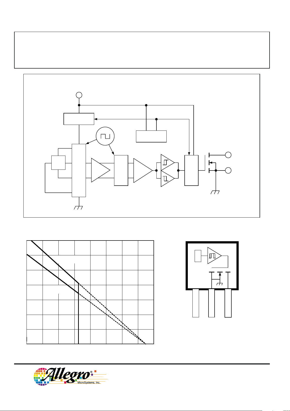
These devices include on a single silicon chip a Hall-voltage generator,
small-signal amplifier, chopper stabilization, a latch, and a MOSFET output.
Advanced BiCMOS processing is used to take advantage of low-voltage and
low-power requirements, component matching, very low input-offset errors,
and small component geometries.
The A3209Ex and A3210Ex are rated for operation over a temperature
range of -40°C to +85°C. Two package styles provide a magnetically optimized package for most applications. Suffix ‘LH’ is a miniature low-profile
surface-mount package while suffix ‘UA’ is a three-lead ultra-mini-SIP for
through-hole or surface mounting.
FEATURES
■ Micropower Operation
■ Operate With North or South Pole
■ 2.5 V to 3.5 V Battery Operation
■ Chopper Stabilized
Superior Temperature Stability
Extremely Low Switch-Point Drift
Insensitive to Physical Stress
■ ESD Protected to 5 kV
■ Solid-State Reliability
■ Small Size
■ Easily Manufacturable With Magnet Pole Independence
Data Sheet
27622.60A
Always order by complete part number: the prefix ‘A’ + the basic four-digit
part number + the suffix ‘E’ to indicate operating temperature range + a
suffix to indicate package style, e.g., A3210ELH .
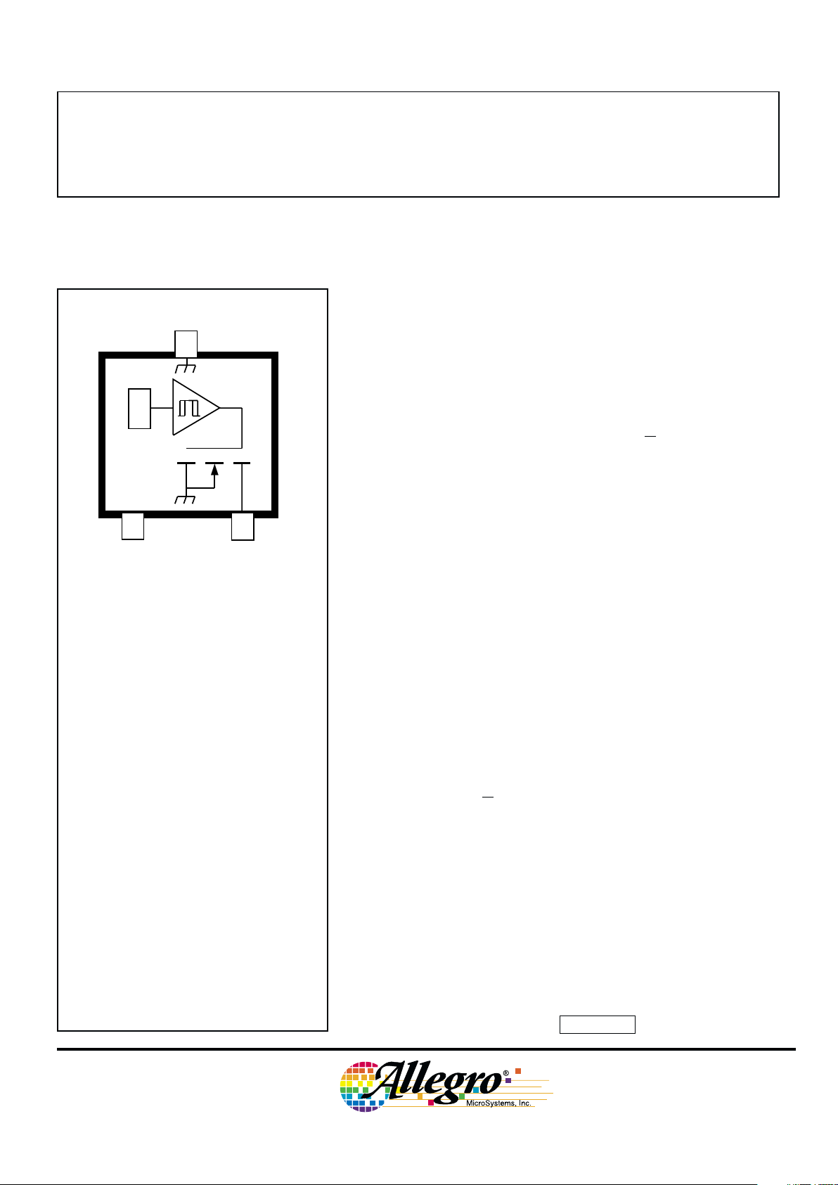
Package Suffix ‘LH’ Pinning
3209
AND
3210
ABSOLUTE MAXIMUM RATINGS
at TA = +25°C
Supply Voltage, VDD............................. 5 V
Magnetic Flux Density, B .......... Unlimited
Output Off Voltage, V
OUT
..................... 5 V
Output Current, I
OUT
.......................... 1 mA
Junction Temperature, TJ............... +170°C
Operating Temperature Range,
TA............................... -40°C to +85°C
Storage Temperature Range,
TS.............................. -65°C to +170°C
Caution: These CMOS devices have input
static protection (Class 3) but are still
susceptible to damage if exposed to
extremely high static electrical charges.
Pinning is shown viewed from branded side.
MICROPOWER, ULTRA-SENSITIVE
HALL-EFFECT SWITCHES
X
Dwg. PH-016-1
SUPPLY
GROUND
OUTPUT
V
DD
12
3
3209
AND
3210
MICROPOWER,
ULTRA-SENSITIVE
HALL-EFFECT SWITCHES
115 Northeast Cutoff, Box 15036
Worcester, Massachusetts 01615-0036 (508) 853-5000
2
FUNCTIONAL BLOCK DIAGRAM
Copyright © 2000, Allegro MicroSystems, Inc.
Package Suffix ‘UA’ Pinning
TIMING
LOGIC
Dwg. FH-020-5
LATCH
GROUND
OUTPUT
SUPPLY
X
DYNAMIC
OFFSET CANCELLATION
SWITCH
SAMPLE
& HOLD
Dwg. PH-016
1
SUPPLY
V
DD
GROUND
32
OUTPUT
X
Pinning is shown viewed from branded side.
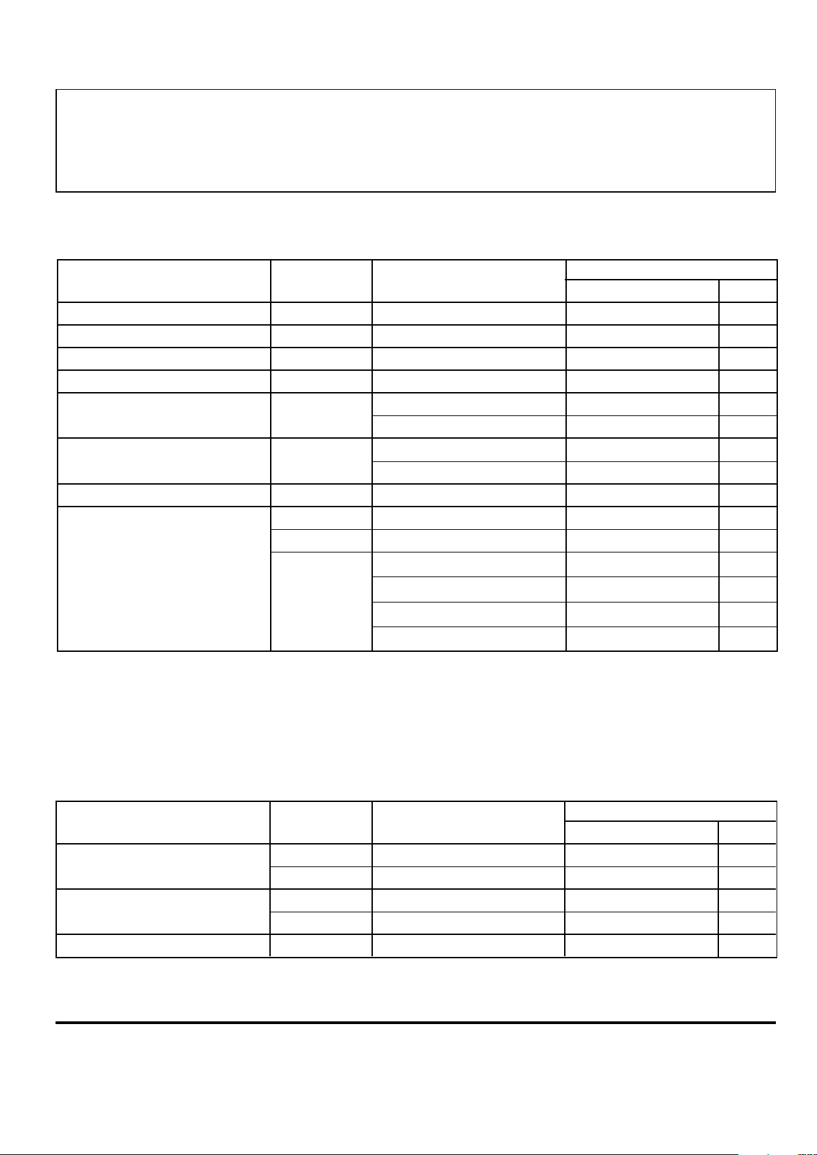
600
400
200
20 60 100
140
0
AMBIENT TEMPERATURE in °C
ALLOWABLE PACKAGE POWER DISSIPATION in MILLIWATTS
Dwg. GH-046-3A
Suffix "UA"
R
θJA
= 206°C/W
40 80 120 180
700
500
300
100
160
Suffix "LH"
R
θJA
= 248°C/W
3209
AND
3210
MICROPOWER,
ULTRA-SENSITIVE
HALL-EFFECT SWITCHES
www.allegromicro.com
3
ELECTRICAL CHARACTERISTICS with C
BYPASS
= 0.1 µF,
over operating voltage and temperature range (unless otherwise specified).
Limits
Characteristic Symbol Test Conditions Min. Typ. Max. Units
Operate Points B
OPS
South pole to branded side – 30 60 G
B
OPN
North pole to branded side -60 -35 – G
Release Points B
RPS
South pole to branded side 5.0 22 – G
B
RPN
North pole to branded side – -27 -5.0 G
Hysteresis B
hys
|B
OPx
- B
RPx
| – 7.7 – G
NOTES: 1. As used here, negative flux densities are defined as less than zero (algebraic convention) and -50 G is less than +10 G.
2. Typical Data is at T
A
= +25°C and VDD = 2.75 V and is for design information only.
MAGNETIC CHARACTERISTICS with C
BYPASS
= 0.1 µF,
over operating voltage and temperature range (unless otherwise specified).
Limits
Characteristic Symbol Test Conditions Min. Typ. Max. Units
Supply Voltage Range V
DD
Operating
1)
2.5 2.75 3.5 V
Output Leakage Current I
OFF
V
OUT
= 3.5 V, B
RPN
< B < B
RPS
– «1.0 1.0 µA
Output On Voltage V
OUT
I
OUT
= 1 mA, VDD = 2.5 V – 105 300 mV
Awake Time t
awake
30 60 90 µs
Period t
period
A3209Ex 240 480 720 µs
A3210Ex 30 60 90 ms
Duty Cycle d.c. A3209Ex – 12.5 – %
A3210Ex – 0.10 – %
Chopping Frequency f
C
– 340 – kHz
Supply Current I
DD(EN)
Chip awake (enabled) 0.1 – 3.0 mA
(2.5 ≤ VDD ≤3.5 V)
I
DD(DIS)
Chip asleep (disabled) 1.0 10 50 µA
I
DD(AVG)
A3209Ex, VDD = 2.75 V – 145 425 µA
A3209Ex, VDD = 3.5 V – 195 425 µA
A3210Ex, VDD = 2.75 V – 8.8 25 µA
A3210Ex, VDD = 3.5 V – 13 60 µA
NOTES: 1. Operate and release points will vary with supply voltage.
2. B
OPx
= operate point (output turns ON); B
RPx
= release point (output turns OFF).
3. Typical Data is at TA = +25°C and VDD = 2.75 V and is for design information only.
3209
AND
3210
MICROPOWER,
ULTRA-SENSITIVE
HALL-EFFECT SWITCHES
115 Northeast Cutoff, Box 15036
Worcester, Massachusetts 01615-0036 (508) 853-5000
4
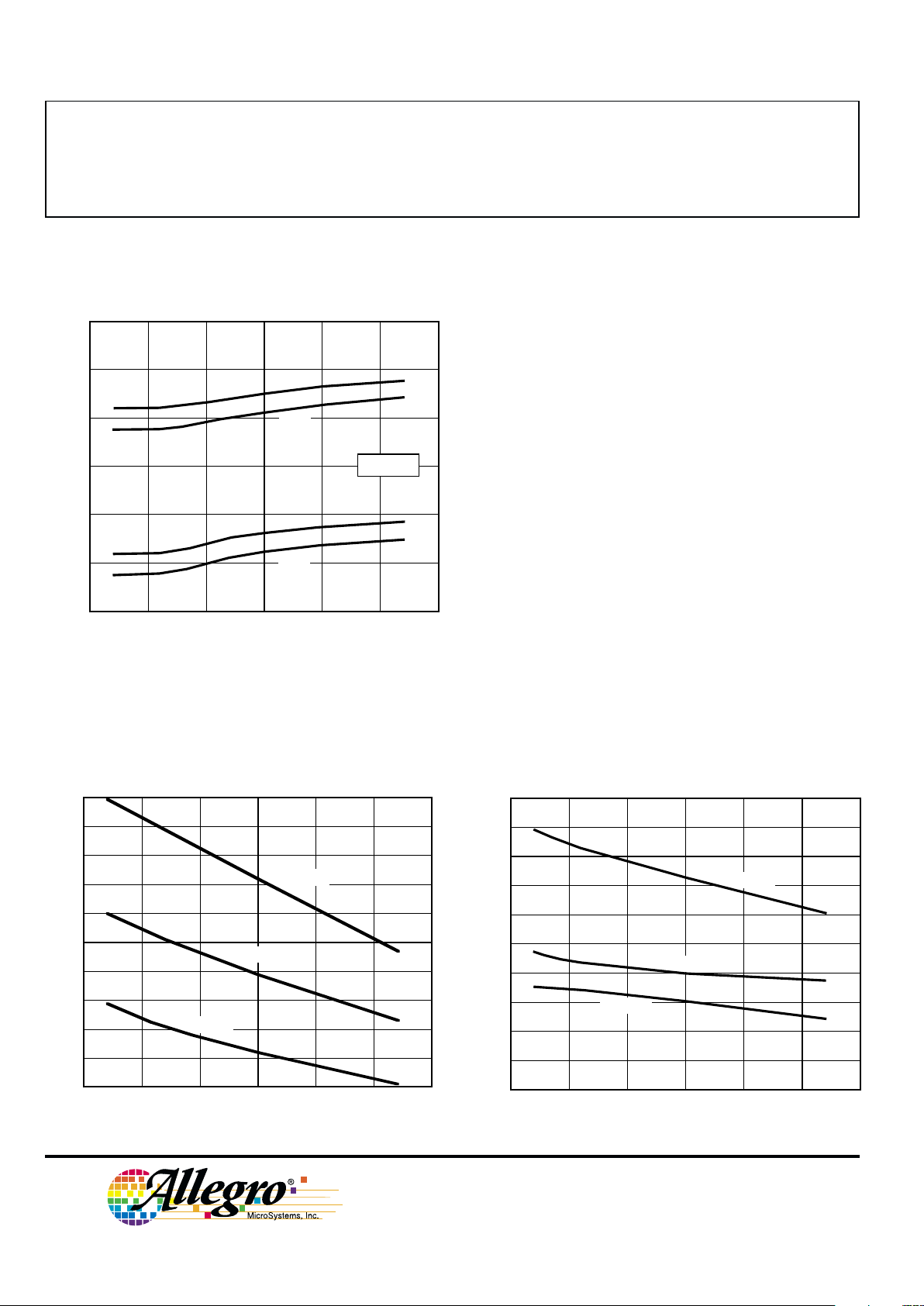
TYPICAL OPERATING CHARACTERISTICS
as a function of temperature
A3210-- SUPPLY CURRENT
SWITCH POINTS
60
SWITCH POINTS IN GAUSS
20
0
-20
-40
0 25 50 75 100
AMBIENT TEMPERATURE IN °C
-50
Dwg. GH-027-2
-25
B
OPS
-60
40
B
RPS
B
RPN
B
OPN
VDD = 2.75 V
16
AVERAGE SUPPLY CURRENT IN µA
12
10
8.0
6.0
0 25 50 75 100
AMBIENT TEMPERATURE IN °C
-50
Dwg. GH-028-6
-25
VDD = 3.5 V
VDD = 2.5 V
14
VDD = 3 V
A3209-- SUPPLY CURRENT
220
AVERAGE SUPPLY CURRENT IN µA
180
160
140
120
0 25 50 75 100
AMBIENT TEMPERATURE IN °C
-50
Dwg. GH-028-7
-25
VDD = 3.5 V
VDD = 3 V
200
VDD = 2.5 V
 Loading...