

Page 1

S
S
S
e
e
e
r
r
r
C
C
C
v
v
v
o
o
o
i
c
i
c
i
c
l
o
l
l
e
e
e
o
o
r
r
r
M
M
M
T
T
T
a
a
a
V
V
V
n
n
n
u
u
u
a
a
a
l
l
l
Page 2

2
Model:
C
C
C
C
C
C
T
T
T
h
h
h
-
-
-
a
a
a
3
3
3
s
s
s
s
s
s
4
4
4
s
i
i
i
C
C
C
s
s
:
:
:
J
J
J
C
C
C
S
S
S
N
N
N
-
-
-
5
5
5
1
1
1
R
R
R
8
8
8
E
E
E
E
E
E
D
D
D
Model no.: CT-34CJ5RE.doc
version 1.0
Page 3

3
CONTENTS
SAFETY INSTRUCTIONS AND MAINTENANCE..........................................................................4
TECHNICAL SPECIFICATION...............................................................................................................................4
PRODUCT SAFETY NOTICE................................................................................................................................. 5
SAFETY SYMBOL DESCRIPTION........................................................................................................................ 7
MAINTENANCE ..................................................................................................................................................... 8
MECHANICA DISASSEMBLES......................................................................................................... 9
ADJUSTMENTS..................................................................................................................................11
SET-UP ADJUSTMENTS.......................................................................................................................................11
CIRCUIT ADJUSTMENTS.................................................................................................................................... 14
STRUCTURE AND CHASSIS FUNCTION DESCRIPTION.........................................................25
STRUCTION BLOCK DIAGRAM......................................................................................................................... 25
BLOCK DIAGRAM FOR SUPPLY VOLTAGE SYSTEM................................................................................... 26
CHASSIS DESCRIPTION...................................................................................................................................... 27
SERVICE DATA..................................................................................................................................28
TECHNICAL DATA OF KEY ICs......................................................................................................................... 28
SERVICE DATA OF KEY ICs............................................................................................................................... 51
APPENDIX............................................................................................54
CIRCUIT DIAGRAM
PARTS LIST
Please read this manual carefully before service.
Model no.: CT-34CJ5RE.doc
version 1.0
Page 4

SERVICE SAFETY AND MAINTENANCE
WARNING:
BEFORE EXAMINING AND SERVICING
THIS CHASSIS READ CAREFULLY THE
FOLLOWING SAFETY
INSTRUCTIONS.
X-RAY RADIATION PRECAUTION
4
1. The EHT must be checked every time the TV is serviced to ensure that the CRT does
not emit X-ray radiation as result of excessive EHT voltage. The maximum EHT voltage
permissible in any operating circumstances must not exceed the rated value. When
checking the EHT, use the High Voltage Check procedure in this manual using an
accurate EHT voltmeter.
2. The only source of X-RAY radiation in this TV is the CRT. The TV minimizes X-RAY
radiation, which ensures safety during normal operation. To prevent X-ray radiation,
the replacement CRT must be identical to the original fitted as specified in the parts list.
3. Some components used in this TV have safety related characteristics preventing the
CRT from emitting X-ray radiation. For continued safety, replacement component
should be made after referring the PRODUCT SAFETY NOTICE below.
4. Service and adjustment of the TV may result in changes in the nominal EHT voltage of
the CRT anode. So ensure that the maximum EHT voltage does not exceed the rated
value after service and adjustment.
Model no.: CT-34CJ5RE.doc
version 1.0
Page 5

5
SAFETY PRECAUTION
WARNING:
REFER SERVICING TO
QUALIFIED SERVICE
PERSONNEL ONLY.
1. The TV has a nominal working EHT voltage. Extreme caution should be exercised when
working on the TV with the back removed.
a. Do not attempt to service this TV if you are not conversant with the precautions
and procedures for working on high voltage equipment.
b. When handling or working on the CRT, always discharge the anode to the TV
chassis before removing the anode cap in case of electric shock.
c. The CRT, if broken, will violently expel glass fragments. Use shatterproof
goggles and take extreme care while handling.
d. Do not hold the CRT by the neck as this is a very dangerous practice.
2. It is essential that to maintain the safety of the customer all power cord forms be replaced
exactly as supplied from factory.
3. Voltage exists between the hot and cold ground when the TV is in operation. Install a
suitable isolating transformer of beyond rated overall power when servicing or connecting
any test equipment for the sake of safety.
4. When replacing ICs, use specific tools or a static-proof electric iron with small power (below
35W).
5. Do not use a magnetized screwdriver when tightening or loosing the deflection yoke
assembly to avoid electronic gun magnetized and decrement in convergence of the CRT.
6. When remounting the TV chassis, ensure that all guard devices, such as nonmetal control
buttons, switch, insulating sleeve, shielding cover, isolating resistors and capacitors,
are installed on the original place.
7. Replace blown fuses within the TV with the fuse specified in the parts list. 8. When
replacing wires or components to terminals or tags, wind the leads around the terminal
before soldering. When replacing safety components identified by the international
hazard symbols on the circuit diagram and parts list, it must be the company-approved
type and must be mounted as the original.
8. Keep wires away from high temperature components.
Model no.: CT-34CJ5RE.doc
version 1.0
Page 6

PRODUCT SAFETY NOTICE
CAUTION:
FOR YOUR PROTECTION
THE FOLLOWING PRODUCT SAFETY NOTICE
SHOULD BE READ CAREFULLY BEFORE
OPERATING AND SERVICING THIS TV SET.
1. Many electrical and mechanical components in this chassis have special safety-related
characteristics. These characteristics are often passed unnoticed by a visual inspection
and the X-ray radiation protection afforded by them cannot necessarily be obtained by
using replacements rated at higher voltages or wattage, etc. Components which have
these special safety characteristics in this manual and its supplements are identified by the
international hazard symbols on the circuit diagram and parts list. Before replacing any of
these components read the parts list in this manual carefully. Substitute replacement
components which do not have the same safety characteristics as specified in the parts list
may create X-ray radiation.
2. Do not slap or beat the cabinet or CRT, since this may result in fire or explosion.
3. Never allow the TV sharing a plug or socket with other large-power equipment. Doing so
may result in too large load, causing fire.
4. Do not allow anything to rest on or roll over the power cord. Protect the power cord from
being walked on, modified, cut or pinched, particularly at plugs.
5. Do not place any objects, especially heavy objects and lightings, on top of the TV set. Do
not install the TV near any heat sources such as radiators, heat registers, stove, or other
apparatus that produce heat.
6. Service personnel should observe the SAFETY INSTRUCTIONS in this manual during use
and servicing of this TV set. Otherwise, the resulted damage is not protected by the
manufacturer.
6
Model no.: CT-34CJ5RE.doc
version 1.0
Page 7
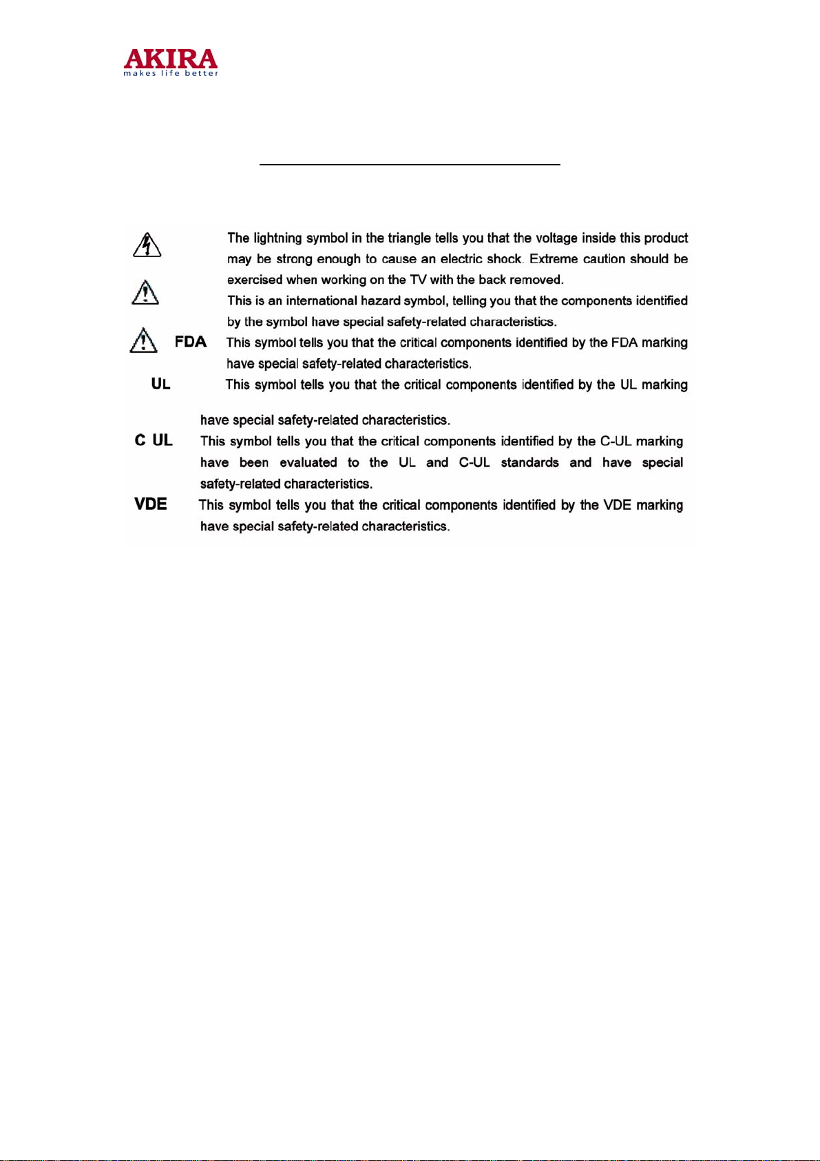
SAFETY SYMBOL DESCRIPTION
7
Model no.: CT-34CJ5RE.doc
version 1.0
Page 8

1. Place the TV set on a stable stand or base that is of adequate size and strength to
prevent it from being accidentally tipped over, pushed off, or pulled off. Do not
place the set near or over a radiator or heat register, or where it is exposed to direct
sunlight.
2. Do not install the TV set in a place exposed to rain, water, excessive dust,
mechanical vibrations or impacts.
3. Allow enough space (at least 10cm) between the TV and wall or enclosures for
proper ventilation.
4. Slots and openings in the cabinet should never be blocked by clothes or other
objects.
5. Please power off the TV set and disconnect it from the wall immediately if any
abnormal condition are met, such as bad smell, belching smoke, sparkling,
abnormal sound, no picture/sound/raster. Hold the plug firmly when disconnecting
the power cord.
6. Unplug the TV set from the wall outlet before cleaning or polishing it. Use a dry soft
cloth for cleaning the exterior of the TV set or CRT screen. Do not use liquid
cleaners or aerosol cleaners.
MAINTENANCE
8
Model no.: CT-34CJ5RE.doc
version 1.0
Page 9
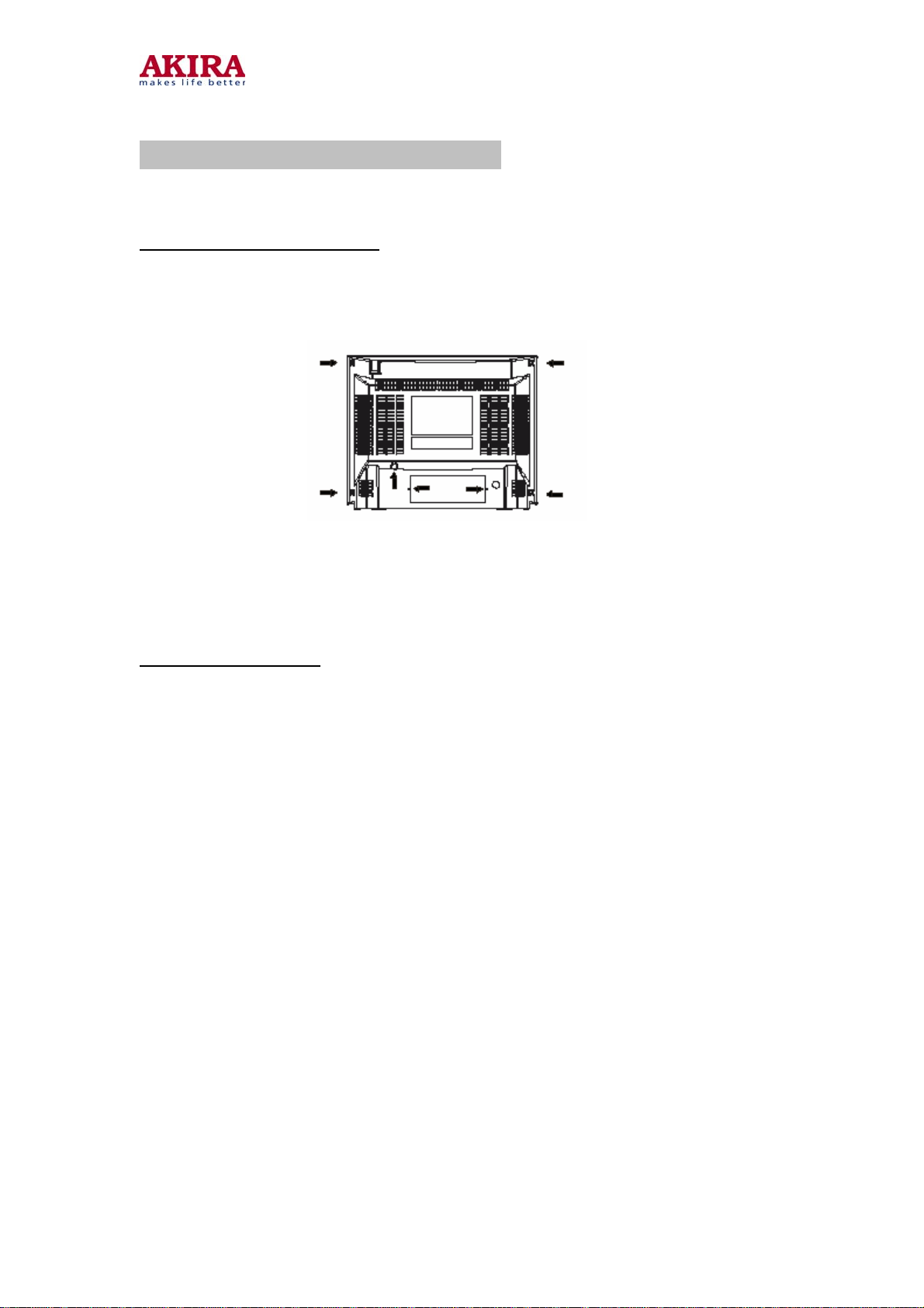
MECHANICA DISASSEMBLIES
CABINET BACK REMOVAL
1. Refer to Figure 1, remove 7screws.
2. Pull off cabinet back and remove.
9
CHASSIS REMOVAL
1. Remove cabinet back.
2. Discharge the picture tube anode (2
grounding lead).
3. Disconnect Degaussing coil socket (KE). Picture tube socket, Deflection yoke connector
(KDY). Speaker connectors (KL and KR), and 2
4. Remove chassis completely by sliding it straight back.
nd
anode lead) to the dag coating (picture tube
nd
anode lead.
Model no.: CT-34CJ5RE.doc
version 1.0
Page 10
10
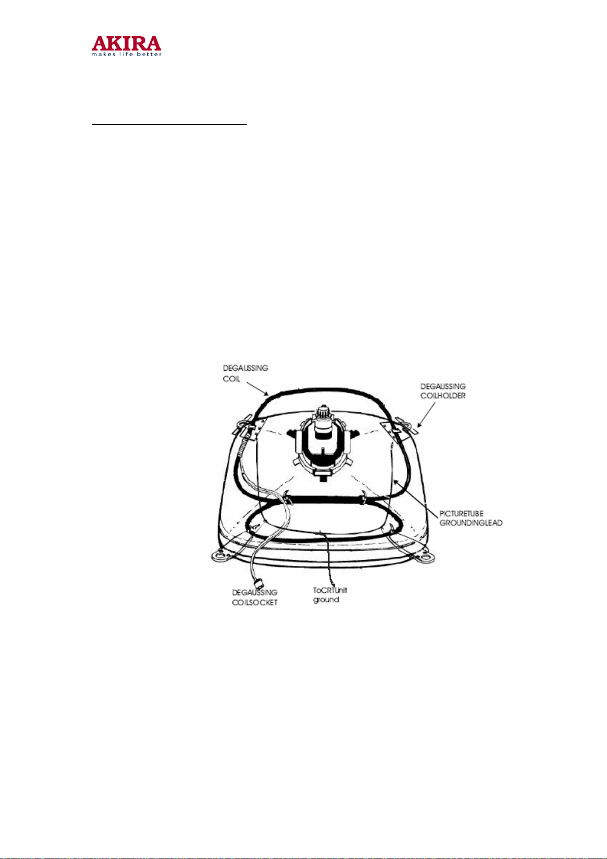
PICTURE TUBE REMOVAL
CAUTION: Do not disturb the deflection yoke or magnet assembly on the picture tube Neck.
Care must be taken to keep these assemblies intact, unless picture tube is being replaced.
Discharge the picture tube to the coating before handing the Tube.
1. Remove chassis, referring to Chassis Removal instructions.
2. Place cabinet front face down on the soft surface.
3. Remove the screw one ach corner of the picture tube and GENTLY lift the picture tube out
of the cabinet.
4. Install a replacement picture tube in reverse order.
5. Properly install the degaussing coil and picture tube grounding lead on the picture tube.
SeeFigure2.
Note: If the Picture Tube is being replaced, mount the Degaussing Coi l on the picture tube. See
following Figure1.Cabinet Back Removal
Model no.: CT-34CJ5RE.doc
version 1.0
Page 11

11
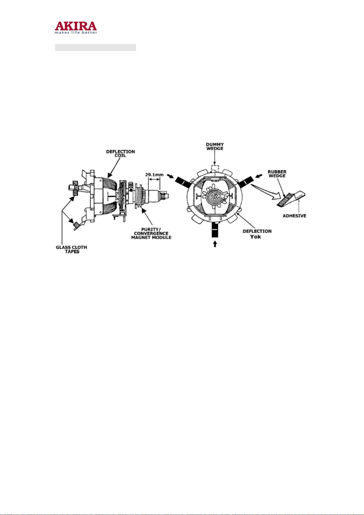
ADJUSTMENTS
SET-UP ADJUSTMENTS
The following adjustments should be made when a complete realignment is required or a new
picture tube is installed.
Perform the adjustments in the following order:
1. Color purity
2. Convergence
3. White balance
Notes:
1. The purity/convergence magnet assembly and rubber wedges need mechanical ositioning.
Refer to Fig1, 2.
2. For some picture tubes, purity/ convergence adjustments are not required.
1. Color Purity Adjustment
Preparation:
Before starting this adjustment, adjust the vertical sync, horizontal sync, vertical amplitude and
focus.
1.1 Face the TV set north or south.
1.2 Connect the power plug into the wall outlet and turn on the main power switch of the TV set.
1.3 Operate the TV for at least 15 minutes.
1.4 Degauss the TV set using a specific degaussing coil.
1.5 Set the brightness and contrast to maximum.
1.6 Counter clockwise rotate the R /B low brightness potentiometers to the end and rotate
the green low brightness potentiometer to center.
1.7 Receive green raster pattern signals.
1.8 Loosen the clamp screw holding the deflection yoke assembly and slide it forward
or backward to display a vertical green zone on the screen. Rotate and spread the
tabs of the purity magnet around the neck of the CRT until the green zone is
located vertically at the center of the screen.
1.9 Slowly move the deflection yoke assembly forward or backward until a uniform
green screen is obtained.
1.10 Tighten the clamp screw of the assembly temporarily. Check purity of the red raster
and blue raster until purities of the three rasters meet the requirement.
Model no.: CT-34CJ5RE.doc
version 1.0
Page 12
12
2. Convergence Adjustment
Preparation:
Before attempting any convergence adjustment, the TV should be operated for at least 15
minutes.
2.1 Center convergence adjustment
2.1.1 Receive dot pattern.
2.1.2 Adjust the brightness/contrast controls to obtain a sharp picture.
2.1.3 Adjust two tabs of the 4-pole magnet to change the angle between them and red and blue
vertical lines are superimposed each other on the center of the screen.
Fig. 1
2.1.4 Turn both tabs at the same time keeping the angle constant to superimpose red and blue
horizontal on the center of the screen.
2.1.5 Adjust two tabs of the 6-pole magnet to superimpose RED/BLUE line and green line.
2.1.6 Remember RED and BLUE movement. Repeat step 2.1.3 ~ 2.1.5 until optimal
convergence is obtained.
2.2 Circumference convergence adjustment
2.2.1 Loosen the clamp screw holding the deflection yoke assembly and allow it tilting.
2.2.2 Temporarily put the first wedge between the picture tube and deflection yoke assembly.
Move front of the deflection yoke up or down to obtain better convergence
in circumference. Push the mounted wedge in to fix the yoke temporarily.
2.2.3 Put the second wedge into bottom.
2.2.4 Move front of the deflection yoke to the left or right to obtain better convergence in
circumference.
2.2.5 Fix the deflection yoke position and put the third wedge in either upper space. Fasten the
deflection yoke assembly on the picture tube.
2.2.6 Detach the temporarily mounted wedge and put it in either upper space. Fasten the
deflection yoke assembly on the picture tube.
2.2.7 After fastening the three wedges, recheck overall convergence and ensure to get optimal
convergence. Tighten the lamp screw holding the deflection yoke assembly.
Model no.: CT-34CJ5RE.doc
version 1.0
Page 13

3. White Balance Adjustment
Generally, white balance adjustment is made with professional equipment. It’s not practical to
get good white balance only through manual adjustment. For TVs with I
the bus data to adjust white balance.
²C bus control, change
13
Fig. 2
Model no.: CT-34CJ5RE.doc
version 1.0
Fig.3
Page 14
14
CIRCUIT ADJUSTMENTS
Preparation:
Circuit adjustments should be made only after completion of set-up adjustments. Circuit
adjustments can be performed using the adjustable components inside the TV set. For TVs with
2C bus control, first change the bus data.
I
1. Degaussing
A degaussing coil is built inside the TV set. Each time the TV is powered on, the
degaussing coil will automatically degauss the TV. If the TV is magnetized by external strong
magnetic field, causing color spot on the screen, use a specific degausser to demagnetize the
TV in the following ways. Otherwise, color distortion will be shown on the screen.
1.1 Power on the TV set and operate it for at least 15 minutes.
1.2 Receive red full-field pattern.
1.3 Power on the specific degausser and face it to the TV screen.
1.4 Turn on the degausser. Slowly move it around the screen and slowly take it away from
the TV.
1.5 Repeat the above steps until the TV is degaussed completely.
2. Confirmation and Adjustment for Voltage
Caution: +B voltage has close relation to high voltage. To prevent X-ray radiation, set +B
voltage to the rated value.
2.1 Power on the TV and receive Philips test pattern.
2.2 Check the resistors and coils for being burned. (If the fuse is burned out, do not power on
the TV again until the cause is found out.)
2.3 Measure voltages of test points with the digital voltmeter. Measure the CRT high voltage
with the high-voltage testing equipment and heater voltage with the high-frequency effective
voltmeter. The rated values are shown as below.
Table 2
Test Point Voltage (V) Test Point Voltage (V)
Negative of VD871
Positive of C879 5±0.5V
Positive of C882 9±0.5V
82V±5V in standby
134±1.5V in use
Positive of C414 5±0.5V
Positive of C412 9±0.5V
16±
Negative of VD872
1V
Positive of C117 32±1V
Negative of VD402A 12.5±1V
Negative of VD404
Heater 6.3+0.2\-0.3Vrms
Model no.: CT-34CJ5RE.doc
version 1.0
27±1.5V
Negative of VD873 16±1V
Negative of VD874 16±1V
Negative of VD403 190±5.0V
CRT anode
29.5KV±1.2KV (only for 29” CRTs)
30.5KV±1.2KV (only for 34” CRTs)
Page 15
15
3. High Voltage Inspection
Caution: No high voltage adjustment components inside the chassis. Please perform high
voltage inspection in the following ways.
3.1 Connect a precise static high voltmeter to the second anode (inside the high voltage cap)
of the CRT.
3.2 Plug in the supply socket (240V AC 50Hz) and turn on the TV. Set the brightness and
contrast to minimum (OµA).
3.3 The high voltage reading should be less than the limited EHT voltage.
3.4 Change the brightness from minimum to maximum, and ensure high voltage not beyond the
Nominal EHT voltage: 29.5±29.51.2KV Limited EHT voltage: 32KV (only for 29” CRTs)
Nominal EHT voltage: 30.5±1.2KV Limited EHT voltage: 35KV (only for 34” CRTs)
4. Focus Adjustment
Caution: Dangerously high voltages are present inside the TV. Extreme caution should be
exercised when working on the TV with the back removed.
4.1 After removing the back cover, look for the FBT on the main PCB. There should be a FCB
on the FBT.
4.2 Power on the TV and preheat it for 15 min.
4 .3 Receive a normal TV signal. Rotate knob of the FCB until you get a sharp picture.
Fig. 4
5. Safety Inspection
5.1 Inspection for insulation and voltage-resistant
Perform safety test for all naked metal of the TV. Supply high voltage of 3000V AC, 50Hz (limit
current of 10mA) between all naked metal and cold ground. Test every point for 3 sec. and
ensure no arcing and sparking.
5.2 Requirements for insulation resistance
Measure resistance between naked metal of the TV and feed end of the power cord to be
infinity with a DC-500 high resistance meter and insulation resistance between the naked metal
and degaussing coil to be over 20M
Model no.: CT-34CJ5RE.doc
version 1.0
Page 16

6. Service Mode
6.1 To enter the SERVICE mode
Set the volume to 0 by the remote control. Then press and hold the MUTE button
on the remote control and MENU button on the TV at the same time for over 2 seconds.
In the S mode, press the POWER button to quit the S mode.
S
16
( “S” is Red and other items are Yellow.)
Use the ↑ ⁄ ↓ bttons on the remote control to highlight an adjustment and the← ⁄ → buttons
to adjust it.
The POS+/-, ↑ ⁄ ↓ , 1~6, RECALL, VOL+/-, MUTE and POWER buttons on the remote control
function in the S mode, but 100+, 7, 8, 9 and 0 buttons not.
Model no.: CT-34CJ5RE.doc
version 1.0
Page 17
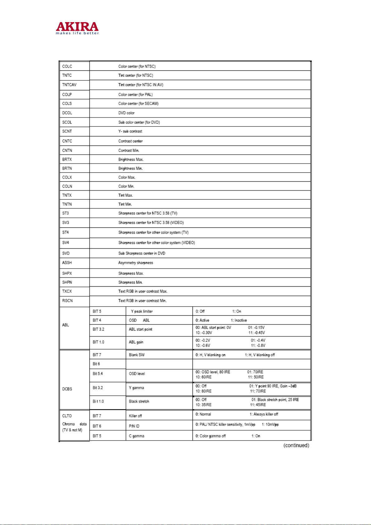
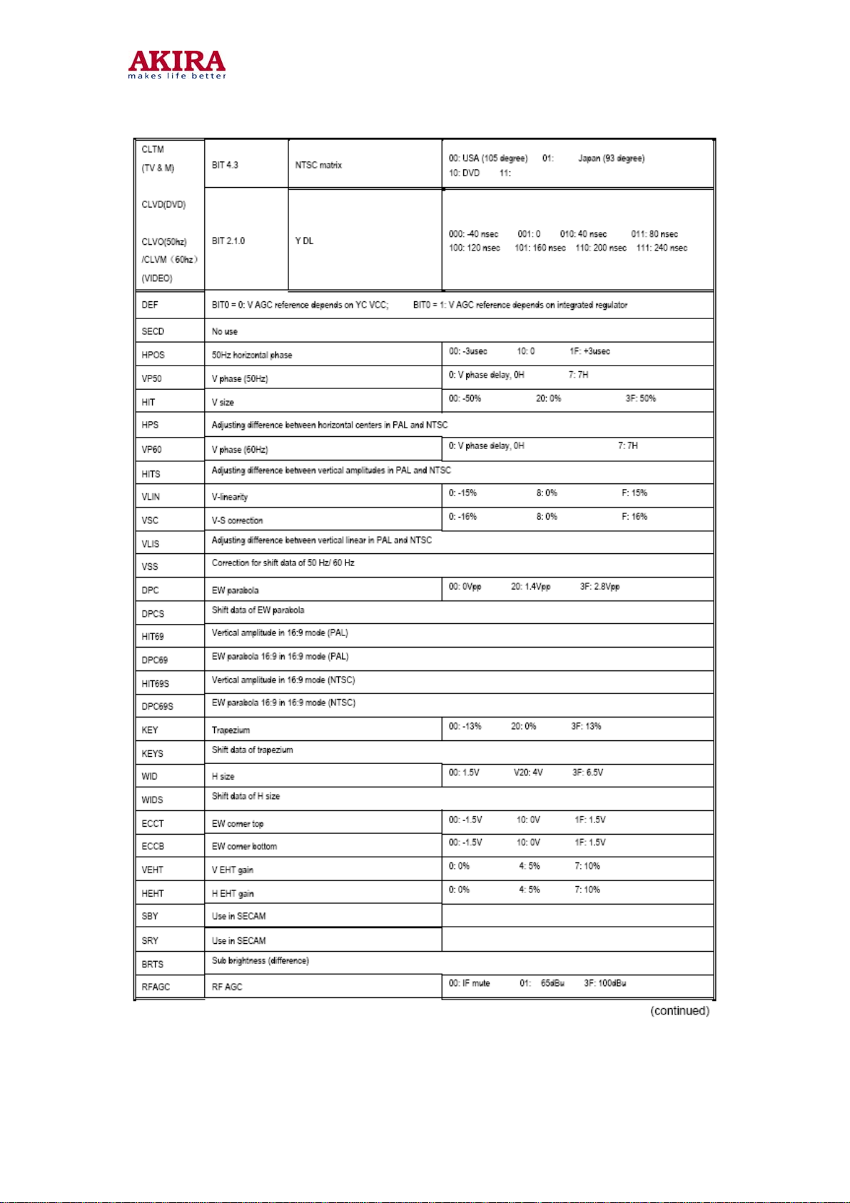
6.2 Adjustments for Service mode and design mode
Table 3
17
Model no.: CT-34CJ5RE.doc
version 1.0
Page 18
18
Model no.: CT-34CJ5RE.doc
version 1.0
Page 19
19
Model no.: CT-34CJ5RE.doc
version 1.0
Page 20
20
Model no.: CT-34CJ5RE.doc
version 1.0
Page 21

21
Model no.: CT-34CJ5RE.doc
version 1.0
Page 22

22
Model no.: CT-34CJ5RE.doc
version 1.0
Page 23

6.3 Adjustment and Bus date
23
Model no.: CT-34CJ5RE.doc
version 1.0
Page 24

24
Model no.: CT-34CJ5RE.doc
version 1.0
Page 25

25
STRUCTURE AND CHASSIS FUNCTION DESCRIPTION
1. STRUCTURE BLOCK DIAGRAM
Model no.: CT-34CJ5RE.doc
version 1.0
Page 26

2. BLOCK DIAGRAM FOR SUPPLY VOLTAGE SYSTEM
26
Model no.: CT-34CJ5RE.doc
version 1.0
Page 27

27
A
A
A
3. CHASSIS DESCRIPTION
General Description
CN-18ED chassis is applied in PF29158E. By use of Toshiba V/C/D -MCU 2IN1 IC for TV small
signal processing and bus control, the chassis enables TV tuning, adjustment, control and picture
correction, featur
compact circuit with fewer external components. The chassis, widely used in small and medium TVs,
provide
2 In 1 IC TMAP8827CSNG with function of E/W correction for PAL small signal processing
and bus control
EEPROM AT24C16 for data memory
s much more convenience for manufacturing and technical service. It includes:
ing high integration, highperformance -to -price ratio and high reliability and
LA78041
TDA8944J for audio power amplifying
Thick-film IC STR-G8656 for power circuit adjustment and control
AV control TC90L01N
The following features are available in the chassis:
Color systems: PAL NTSC SECAM
Sound systems: B/G D/K I M
236 programs preset
Multilingual on screen display
²C bus control
I
AV Stereo
Game
Biorhythm
Calendar inquiry
The chassis mainly uses the following ICs and assemblies.
for vertical output power amplifying
Table 5 Key ICs and Assemblies
No. Position Type Description
1 N230
2 N210 CH08T0605 (A8827CSNG5BK0 ) 2IN1 IC (Small signal processor + micro control (UOC))
3 N601 TA1343N
4 N603 TDA8944J Stereo audio power amplifier
5 N301 LA78041 Vertical scan output stage circuit
6 N801 STR-G8656 Switch-mode power supply control
7 N901 TC90L01N
8 A101 TDQ-5B4 M Tuner
Model no.: CT-34CJ5RE.doc
version 1.0
T24C016 EERPOM
udio processor
V switch
Page 28

28
SERVICE DATA
TECHNICAL DATA OF KEY ICs
1. TOSHIBA 2IN1 IC SERIES TMPA8827CMNG /CPNG/CSNG
MCU AND SIGNAL PROCESSOR FOR A PAL/NTSC/SECAM TV
The TMPA8827CMNG /CPNG /CSNG is an integrated circuit for a PAL/ NTSC/SECAM TV. A
MCU and a TV signal processor are integrated in a 64-pin shrink DIP package. The MCU
contains 8-bit CPU, ROM, RAM, I/O ports, timer/ counters, A/D converters, an on-screen
display controller, remote control interfaces, IIC bus interfaces and the Closed Caption decoder.
The TV signal processor contains PIF, SIF, Video, multi-standard chroma, Deflection, RGB
processors.
MROM: TMPA8827CMNG (ROM:32K)
TMPA8827CPNG (ROM:48K)
TMPA8827CSNG (ROM:64K)
OTP:TMPA8827SNG
Weight : 8.85g (typ.)
1) Features
MCU
High speed 8 bit CPU (TLCS-870/X series)
Instruction execution time:0.5 µ s (at 8MHz)
(TMPA8827CMNG)
32-Kbytes ROM, 2-Kbytes RAM
(TMPA8827CPNG)
48-Kbytes ROM,2-Kbytes RAM
(TMPA8827CSNG)
64-Kbytes ROM,2-Kbytes RAM
ROM correction
12 I/O ports
14bit PWM output 1 ch for a voltage
Synthesizer
7-bit PWM output 1 channel
8-bit A/D converter 3 ch for a touch key input
with Key ON wake-up CIRCUIT
Remote control signal preprocessor
Two 16-bit internal timer / counter 2 ch
Two 8-bit internal timer / counter 2 ch
Time base timer,watchdog timer
16 interrupt sources:external 5, internal 11
IIC bus interface (multi-master)
TV Processor
Model no.: CT-34CJ5RE.doc
version 1.0
Page 29

CCD Decorder
Digital data slicer for NTSC
OSD
Clcok generation for OSD display
Font ROM charaters:384 charaters
Charaters display:32 columns x 12 lines
Composition: 16 x 18 dots
Size of charaters: 3 (line by line)
Color of charaters: 8 (charaters by charater)
Display position:H 256/V 512 steps
Box function
Fringing, smoothing, Italic, underline
function
Conform to CCD REGULATION
Jitter elimination
IF
Intergrated PIF VCO aligned auto
Negative demodulation PIF
Multi-frequency SIF demodulator without external Tank-coil
Video
Integrated chroma traps
Chroma
Intergrated chroma BPFs
PAL / NTSC / SECAM demodulation
RGB / Base – Band
Intergrated 1 H base-band delay line
Base-band TINT control
Internal OSD interface
Half-tone and transparent for OSD
External YCbCr interface for DVD
RGB cut-off / drive controls by bus
ABCL (ABL and ACL combined)
Sync.
Integrated fH x 640 VCO
DC coupled vert. ramp output (single)
EW correction with EHT input
29
Model no.: CT-34CJ5RE.doc
version 1.0
Page 30

2) Block Diagram
30
Model no.: CT-34CJ5RE.doc
version 1.0
Fig. 8 Block Diagram
Page 31

31
3) Basic Structure
3.1) Internal Connections
TMPA8827 has two pieces of IC chip in one package, using Multi-Chip-Package (MCP)
technology. One is a micro controller (MCU) and the other one is a signal processor (SP) for a
color TV. There are some internal connections between these two ICs for handling below
signals.
Table 6 Signal Name Direction Description
No. Signal Name Direction Description
1 SCL M to S Internal IIC bus SCL
2 SDA Bi-direction Internal IIC bus SDA
3 OSD R M to S OSD signal connection
4 OSD G M to S OSD signal connection
5 OSD B M to S OSD signal connection
6 OSD Y/BL M to S OSD display control
7 OSD I, CS
OUT
8 C-Video S to M Composite video signal from internal video switch, for
9 C-Sync S to M Composite sync. signal from sync. Separator, for CCD
10 HD S to M Horizontal timing pulse regenerated from FBP, for OSD
11 VD S to M Vertical timing pulse from sync. Separator, for OSD
12 CLK M to S 8 MHz clock
13 AVDD M to S Reference voltage for C-Video interface
14 ADC S to M A/D converter monitoring RF-AGC, R-Y and B-Y
Functions of SP from MCU are controllable through the IIC bus of the internal connections.
3.2) Power Supply
TMPA8827 has some power supply and GND pins. Power supplies related MCU must be
applied at the first. Power supplies for H.VCC and TV D.VCC are the second with at least 100
ms delay after MCU power ON. The other power supplies are the last, which are recommended
to be supplied from a regulator circuit using FBP.
3.3) Crystal Resonator
solution requires two resonators at least, one for MCU and the other one for SP. An oscillation
clock with the crystal resonator of TMPA8827is supplied for MCU operation, PIF VCO
automatic alignment, alignment free AFT, chroma demodulation and horizontal oscillation. The
oscillation frequency is very important so that those of functions work properly, so that
designing the oscillation frequency
accurately is required. The spec of crystal is recommended to be within
fosc: 8 MHz +/-20 ppm
ftemp: 8 MHz +/-40 ppm (-20°C to +65°C)
While RESET of MCU is active, the MCU function stops. Hardware and software initialization
sequence including power supplies control is required, because status of any hardware after
the RESET period is unknown especially horizontal oscillator which is a very basic timing
generator of SP operation.
TMPA8827 requires only one crystal resonator, in stead that a conventional two-chip
M to S OSD half-tone control/Test pattern signal
CCD
Model no.: CT-34CJ5RE.doc
version 1.0
Page 32

4) Terminal Interface
MCU Block
32
Model no.: CT-34CJ5RE.doc
version 1.0
Page 33

33
Model no.: CT-34CJ5RE.doc
version 1.0
Page 34

34
Model no.: CT-34CJ5RE.doc
version 1.0
Page 35

35
Model no.: CT-34CJ5RE.doc
version 1.0
Page 36

36
2. AUDIO POWER AMPLIFIER TDA8944J
2 X 7 W STEREO BRIDGE TIED LOAD (BTL) AUDIO AMPLIFIER
1) General Description
The TDA8944J is a dualchannel audio power amplifier with an output power of 2 x 7 W at an 8Ω
load and a 12 V supply. The circuit contains two Bridge Tied Load (BTL) amplifiers with an
all-NPN output stage and standby/mute logic. The TDA8944J comes in a 17 -pin DIL -bent-SIL
(DBS) power package. The TDA8944J is printed-circuit board (PCB) compatible with all other
types in the TDA894x family. One PCB footprint accommodates both the mono and the stereo
products.
2) Features
Few external components
Fixed gain
Standby and mute mode
No on/off switching plops
Low standby current
High supply voltage ripple rejection
Outputs short-circuit protected to ground, supply and across the load
Thermally protected
Printed-circuit board compatible.
3) Blaock Diagram
Model no.: CT-34CJ5RE.doc
version 1.0
Page 37

4) Pinning Information
37
Model no.: CT-34CJ5RE.doc
version 1.0
Page 38

38
3. VERTICAL SCAN OUTPUT STAGE CIRCUIT LA78041
Both LA78040/LA78041 are vertical scan output stage power amplifiers. But there
is a little bit difference between the two amplifiers, that is, LA78040 has supply voltage of
24V and output current of 1.8AP-P while LA78041 has supply voltage of 30V and output
current of 2.2AP-P. LA78041 (N301)
Vertical Deflection Output Circuit
1) Features
Low power dissipation due to built-in pump-up circuit Vertical output circuit
Thermal protection circuit built in Excellent crossover characteristics DC coupling possible
2) Block Diagram
Package Type:TO-220-7H
Fig.12
Model no.: CT-34CJ5RE.doc
version 1.0
Fig.1 3 Block diagram
Page 39

39
4. EPROM AT24C04/08/ 16
1) Features
Low-voltage and Standard-voltage Operation
-2.7 (Vcc=2.7V to 5.5V)
-1.8 (Vcc=1.8V to 5.5V)
Internally Organized 128x8(1K), 256x8 (2K), 512x8 (4K), 1024x8 (8K) or 2048x8 (16K)
2-wire Serial Interface
Schmitt Trigger, Filtered Inputs for Noise Suppression Bi-directional Data Transfer Protocol
100kHz (1.8V, 2.5V, 2.7V) and 400 kHz (5V) Compatibility
Write Protect Pin for Hardware Data Protection
8-byte Page (1K, 2K), 16-byte Page (4K, 8K, 16K) Write Modes Partial Page Writes are allowed
Self-timed Write Cycle (10 ms max)
High-reliability
- Endurance: 1 Million Write Cycles
- Data Retention: 100 Years
Automotive Grade and Extended Temperature Devices Available
8-lead PDIP, 8 -lead JEDEC SOIC, 8 -lead MAP and 8 -lead TSSOP Package
2-wire
Serial EEPROM
AT24C01A 1K (128 x 8)
AT24C02 2K (256 x 8)
AT24C04 4K (512 x 8)
AT24C08 8K (1024 x 8)
AT24C16 6K (2048 x 8)
2) Description
The AT24C01A/02/04/08/16 provides 1024/2048/4096/8192/16384 bits of serial electrically
erasable and programmable read-only memory (EEPROM) organzed as 128/256/512/1024/2048
words of 8 bits each. The device is optimized for use in many industrial and commercial applications
where low-power and low-voltage operations are essential. The AT24C01A/02/04/08/16 is available
in space -saving 8 -pin PDIP, 8 -lead JEDEC SOIC, 8 -lead MAP and 8-lead TSSOP packages and
is accessed via a 2-wire serial interface. In addition, the entire family is available in 2.7V (2.7V to
5.5V) and 1.8V (1.8V to 5.5V) versions.
Model no.: CT-34CJ5RE.doc
version 1.0
Page 40

3) Pin Configuration
40
Table 10
Fig. 14
Fig. 15
4) Pin Description
SERIAL CLOCK (SCL): The SCL input is used to positive edge clock data into each EEPROM
device and negative edge clock data out of each device.
SERIAL DATA (SDA): The SDA pin is bi-directional for serial data transfer. This pin is opendrain
driven and may be wired with any number of other open-drain or open-collector devices.
DEVICE / PAGE ADDRESSES (A2, A1, A0): The A2, A1 and A0 pins are device address inputs that
are hard wired for the AT24C01A and the AT24C02. As many as eight 1K/2K devices may be
addressed on a single bus system (device addressing is discussed in detail under the Device
Addressing section).
The AT24C04 uses the A2 and A1 inputs for hard wire addressing and a total of four 4K devices may
be addressed on a single bus system. The A0 pin is a no connect.
The AT24C08 only uses the A2 input for hardwire addressing and a total of two 8K devices may be
addressed on a single bus system. The A0 and A1 pins are no connects.
The AT24C16 does not use the device address pins, which limits the number of devices on a single
bus to one. The A0, A1 and A2 pins are no connects.
Model no.: CT-34CJ5RE.doc
version 1.0
Page 41

41
WRITE PROTECT (WP): The AT24C01A/02/04/16 has a Write Protect pin that provides
hardware data protection. The Write Protect pin allows normal read/write operations when
connected to ground (GND). When the Write Protect pin is connected to Vcc, the write
protection feature is enabled and operates as shown in the following table.
Table 11
WP Pin Part of the Array Protected
24C08
Status
At Vcc
At GND Normal Read/Write Operations
5) Memory Organization
AT24C01A, 1K SERIAL EEPROM: Internally organized with 16 pages of 8 bytes each, the 1K
requires a 7 -bit data word address for random word addressing.
AT24C02, 2K SERIAL EEPROM: Internally organized with 32 pages of 8 bytes each, the 2K
requires an 8 -bit data word address for random word addressing.
AT24C04, 4K SERIAL EEPROM: Internally organized with 32 pages of 16 bytes each, the 4K
requires a 9 -bit data word address for random word addressing.
AT24C08, 8K SERIAL EEPROM: Internally organized with 64 pages of 16 bytes each, the 8K
requires a 10 -bit data word address for random word addressing.
AT24C16,16K SERIAL EEPROM: Internally organized with 128 pages of 16 bytes each, the 16K
requires an 11-bit data word address for random word addressing.
6) Block Diagram
24C01A
Full (1K)
Array
24C02
Full (2K)
Array
24C04
Full (4K)
Array
Normal
Read/
Write
Operation
24C16
Upper
Half
(8K)
Array
Model no.: CT-34CJ5RE.doc
version 1.0
Fig.16 Block Digram
Page 42

5. SWITCH -MODE POWER SUPPLY IC STRG5653/G8656
1) General Description
The STRG5653/G8656 are part of the STRG5600/G8600 series thick-film ICs for switch-mode
power supply incorporating power MOSFET with a high-precise error amplifier. The ICs feature
fewer external components, small-size and standard power supply.
The series STR-G8600 use Chip on Chip technology with the same operation principle as
STR-G5600. Pin configuration, function and threshold of STR-G8600 are compatible with those of
STR-G5600.
42
Model no.: CT-34CJ5RE.doc
version 1.0
Page 43

6. TC9 0L01N
AUDIO / VIDEO SWITCHING IC FOR TVs
The TC90L01N is an audio/video switching IC
for TV sets. Conforming to I
it allows you to perform various switching
operations through the bus lines by using a
microcomputer. This IC has the functions of
audio mute, ALC (Auto Level Control), audio
volume and so on.
1) Features
²C bus control
· I
Video: 3-channel input abd 1-channel
outputs
(1 channels conforming to S system)
Audio: 3-channel inputs and 3-channel
outputs
Monitor Audio out
ALC (Auto Level Control)
Audio Volume by attenuator circuit
Audio mute
2 I/O ports
2C bus standards,
2) Pin Assignment
Fig. 18
43
Model no.: CT-34CJ5RE.doc
version 1.0
Fig.19 Pin Assignment
Page 44

3). Block Diagram
44
Model no.: CT-34CJ5RE.doc
version 1.0
Fig. 20 Block Diagram
Page 45

4) Pin Description
45
Model no.: CT-34CJ5RE.doc
version 1.0
Page 46

46
Model no.: CT-34CJ5RE.doc
version 1.0
Page 47

47
Model no.: CT-34CJ5RE.doc
version 1.0
Page 48

7. TA1343N
48
Model no.: CT-34CJ5RE.doc
version 1.0
Page 49

2) Block Diagram
49
Fig.21
Model no.: CT-34CJ5RE.doc
version 1.0
Page 50

3) Terminal Function
50
Table 14
Model no.: CT-34CJ5RE.doc
version 1.0
Page 51

SERVICE DATA OF KEY ICs
Table 15 Functions and Service Data of A8827CSNG5BK0 (N210)’s Pins
Pin No. 1 2 3 4 5 6 7 8
Voltage (V)
Resistance (KΩ)
Pin No. 9 10 11 12 13 14 15 16
Voltage (V)
Resistance (KΩ)
Pin No. 17 18 19 20 21 22 23 24
Voltage (V)
Resistance (KΩ)
Pin No. 25 26 27 28 29 30 31 32
Voltage (V)
Resistance (KΩ)
Pin No. 33 34 35 36 37 38 39 40
Voltage (V)
Resistance (KΩ)
Pin No. 41 42 43 44 45 46 47 48
Voltage (V)
Resistance (KΩ)
Pin No. 49 50 51 52 53 54 55 56
Voltage (V)
Resistance (KΩ)
Pin No. 57 58 59 60 61 62 63 64
Voltage (V)
Resistance (KΩ)
3.9 ~ 4.8 4.5~4.9 5 0 5 2.22 2 0
8.8 8.8 22 0 4.55 22.8 22.7 0
5 0 0 1.22 1.87 6.63 4.16 5
3.6 0 0 35.7 0.79 36.3 36.3 15.6
9 2 2.45 2.61 2.44 0 2.44 2.61
10 26 26 26 26 0 26 26
3.4 1.9 4.58 4.78 9.0 3.44 1.77 3.48
10.3 26 24.2 22.9 0.39 3.32 3.3 24.17
2.97 2.44 2.49 4.96 2.2 4.39 1.8 0
26 24.8 26 1.6 20 22.8 26 0
0.12 0.12 1.8 4.9 2.76 3.5 2.4 0
26 26 12.9 1.6 26 26 26 0
8.88 2 2 2 0 0 5 0.086
0.40 23.1 23.1 23.1 0 0 3.52 8.2
5 5 5 4.38 0 4.29 0.23 0.027
13.7 13.7 12 22.6 24.92 20.4 24.85 6.7
51
Model no.: CT-34CJ5RE.doc
version 1.0
Page 52

Table 16 Functions and Service Data of TDA8944J (N603)’s Pins
Digital Multimeter
Measure with
Pin
No.
1
Function Description
Negative Loudspeaker
Terminal
Ref.
Voltage
(V)
7.98 10 2.47
RED
probe while
grounding
Black probe
(KΩ)
2 Ground Channel 1 0 0 0
3 Supply Voltage Channel 1 15.79 7.17 1.7
Positive Loudspeaker
4
Terminal
7.84 11 2.44
5 Not Connected 0 ∞ ∞
6 Positive Input 1 7.85 16 3
7 Not Connected 0 ∞ ∞
8 Negative Input 1 7.85 15.7 3
9 Negative Input 2 7.64 15.7 3
Mode Selection Input
10
(standby, Mute, Operating)
0.21 18.6 2.89
Half Supply Voltage
11
Decoupling (Ripple
7.84 16.2 2.87
Rejection)
12 Positive Input 2 7.62 17 2.88
13 Not Connected 0 ∞ ∞
Negative Loudspeaker
14
Terminal 2
7.84 11 2.44
15 Ground Channel 2 0 0 0
16 Supply Voltage Channel 2 15.80 7.17 1.7
Positive Loudspeaker
17
Terminal 2
7.82 11 2.44
Table 17 Functions and Service Data of LA78041 (N301)’s Pins
GDM8145 Multimeter
Pin
No.
1
2 VCC 27.68 - 1.87
3
4 GND 0 0 0
5 Ver. OUTPUT 16.35 - 2.26
6
7
Function
Description
INVERTING
INPUT
PUMP UP
OUT
OUTPUT
STAGE Vcc
NON
INV.INPUT
Voltage of
Pin (V)
2.87 - 2.62
2.32 - 2.68
28.23
2.88 3.25 2.5
Measure with Red
probe while grouding
Ground Resistance (KΩ)
Measure with Black
probe while grouding
black probe
∞
Mearsure with
Black
probe while
grouding RED
probe (KΩ)
Red probe
2.35
52
Model no.: CT-34CJ5RE.doc
version 1.0
Page 53

53
Table 18 Functions and Service Data of AT24C16 (N230)’s Pins
Digital Multimeter
Pin
No.
1 Address Input 0 0 0
2 Address 0 0 0
3 Address 0 0 0
4
5 Clock Line 5 13.79 11.22
6 Data Line 5 13.70 13.13
7
8
Function
Description
Common
Ground
PW Write
Protect
Supply
Voltage
Ref.
Voltage
(V)
0 0 0
0 0 0
5 3.79 3.78
Table 19 Functions and Sevice Data of STR-G8656 (N801)’s Pins
Pin
No.
Functions Description
1 Drain Terminal 295 ∞ ∞
2 Source Terminal 0.024 0 0
3 Ground Terminal 0 0 0
4 Power Supply Terminal 32.1 ∞ 1.838
Overcurrent / Freback
5
Terminal
Measure with Red
probe while
Grounding Black
probe (KΩ)
Measure with Black probe
while grounding Red probe
(KΩ)
Digital Multimeter
Measure with
Ref. Voltage
(V)
Black probe (KΩ)
1.96 0.68 0.68
Red
Probe while
grounding
Measure with
Black
probe while
grounding
Red probe (KΩ)
Model no.: CT-34CJ5RE.doc
version 1.0
Page 54

54
APPENDIX
Model no.: CT-34CJ5RE.doc
version 1.0
Page 55

Speaker
Wired Connector XP205's A
Blue
Bla k
dRe
la kB c
Control Buttons Board Assembly
c
From Power Switch Assembly
XP803
XP804
XS901A
Remote Sensor PCB Assembly
Wired Connector AwD-02-700
Speaker
XPK01B
Wired Connector XP205's B
To Degaussing Coil
XP801
XS801
XP801
Wired Connector XS703A
XP200B
Wired Connector XP205
XP603
XP205
White
Black
eR d
Black
+
-
+
-
Power PCB Assembly
XP400
To Deflection Yoke
XP403
Wired connector XE01
XP200D
XP202
XP904
AV PCB Assembly
AD-04-480(V2)
XP201
XP903
XP908
XP901B
Screen Wire (Grey)
CRT's Ground Wire
(Soldered)
First soldered the focus wire,
then close the cover.
Wired connector AD-06-380
B
P903
Focus Wire (Red)
A2
A1
CRT RGB PCB assembly
P902A
Side-set AV PCB Assembly
Design
Examine
Standards
Approve
Tracing Width: A3
Page 56

This circuit diagram is only for reference, specifications are subject to change without reference.
Page 57

57
REPLACEMENT PARTS LIST
PART CODE PART NAME SPECIFICATION QTY LOCATION
56282105102 SPEAKER
BC602
562J1110080 SPEAKER
BC606
50640063030
C689A
DEGAUSSING COIL 1 XP804
54111A04650 POWER SWITCH KDC-A04(S) 1 SPB801
54111A04650 POWER SWITCH PS5E-A
54111A04650 POWER SWITCH KDC-A04-MU169
34" CRT 1
FRONT PANEL 1
883370288G001 POWER S JUC8.337.288-G001 1
883370289G006 FUNCTION KEY JUC8.337.289-G006 1
8864001550C LENS JUC8.640.155 1
820180263108L REMOTE CONTROLLER K18F-C108 1
87820111701C MAIN PCB JUC7.820.1117 1
51113100JU0 CARBON RES.
50620071680 CARBON RES.
51113470JU0 CARBON RES.
51113750JU0 CARBON RES.
51113101JU0 CARBON RES.
R204 R207 R212 R213 R222
R233 R238 R241 R243 R253
R255 R256 R258 R259 R263
51113151JU0 CARBON RES.
51113181JU0 CARBON RES.
51113221JU0 CARBON RES.
50620071630 CARBON RES.
51113391JU0 CARBON RES.
51113471JU0 CARBON RES.
50620071910 CARBON RES.
51113102JU0 CARBON RES.
R257 R410 R437 R879 R262
51113122JU0 CARBON RES.
50620073070 CARBON RES.
51113222JU0 CARBON RES.
51113332JU0 CARBON RES.
51113472JU0 CARBON RES.
R247 R610
50620071870 CARBON RES.
51113822JU0 CARBON RES.
51113103JU0 CARBON RES.
R327 R407 R409 R411 R608
R875 R876
51113123JU0 CARBON RES.
51113153JU0 CARBON RES.
51113223JU0 CARBON RES.
51113273JU0 CARBON RES.
50620071720 CARBON RES.
51113333JU0 CARBON RES.
50620071780 CARBON RES.
51113473JU0 CARBON RES.
51113513JU0 CARBON RES.
51113563JU0 CARBON RES.
50620072050 CARBON RES.
51113104JU0 CARBON RES.
50620071490 CARBON RES.
51113224JU0 CARBON RES.
50620071620 CARBON RES.
50620072030 CARBON RES.
51113105JU0 CARBON RES.
50620071270 CARBON RES.
50620071370 CARBON RES.
50620071290 CARBON RES.
50620101340 METAL OXIDE FILM RES.
50620101010 METAL OXIDE FILM RES.
50620101410 METAL OXIDE FILM RES.
50620101440 METAL OXIDE FILM RES.
50620101460 METAL OXIDE FILM RES.
50620100970 METAL OXIDE FILM RES.
50620101550 METAL OXIDE FILM RES.
YDT416-N-10W-8Ω
YDG52-A1-10W-8Ω
CD71-50V-1μFM
RT13-0.166W-10ΩJ
RT13-0.166W-27ΩJ
RT13-0.166W-47ΩJ
RT13-0.166W-75ΩJ
RT13-0.166W-100ΩJ
RT13-0.166W-150ΩJ
RT13-0.166W-180ΩJ
RT13-0.166W-220ΩJ
RT13-0.166W-240ΩJ
RT13-0.166W-390ΩJ
RT13-0.166W-470ΩJ
RT13-0.166W-560ΩJ
RT13-0.166W-1KΩJ
RT13-0.166W-1.2KΩJ
RT13-0.166W-2KΩJ
RT13-0.166W-2.2KΩJ
RT13-0.166W-3.3KΩJ
RT13-0.166W-4.7KΩJ
RT13-0.166W-5.6KΩJ
RT13-0.166W-8.2KΩJ
RT13-0.166W-10KΩJ
RT13-0.166W-12KΩJ
RT13-0.166W-15KΩJ
RT13-0.166W-22KΩJ
RT13-0.166W-27KΩJ
RT13-0.166W-30KΩJ
RT13-0.166W-33KΩJ
RT13-0.166W-39KΩJ
RT13-0.166W-47KΩJ
RT13-0.166W-51KΩJ
RT13-0.166W-56KΩJ
RT13-0.166W-82KΩJ
RT13-0.166W-100KΩJ
RT13-0.166W-150KΩJ
RT13-0.166W-220KΩJ
RT13-0.166W-240KΩJ
RT13-0.166W-820KΩJ
RT13-0.166W-1MΩJ
RT14-0.25W-220ΩJ
RT14-0.25W-680ΩJ
RT14-0.25W-3.3KΩJ
RY21-0.5W-1ΩJ
RY21-0.5W-8.2ΩJ
RY21-0.5W-270ΩJ
RY21-0.5W-3.9KΩJ
RY21-0.5W-4.7KΩJ
RY21-0.5W-820KΩJ
RY21-1W-18ΩJ
2 BC601
2 BC605
2 C688A
1 R136
1 R134
2 R245 R066
2 R605 R606
20 R103 R104 R122 R202 R203
1 R214
1 R140
3 R244 R607 R878
1 R415
1 R447
1 R249
4 R401 R402 R406 R415A
10 R101 R102 R232 R254 R256A
2 R130 R135
2 R611 R612
2 R242 R805
3 R210 R211 R405
7 R131 R222A R234 R236 R237
2 R322 R448
2 R248 R200
12 R118 R120 R224 R226 R231
2 R117 R320
5 R123 R449 R440A R680 R682
1 R114
1 R414
1 R218
2 R119 R239
1 R801
3 R615 R874 R877
1 R328
3 R121 R413 R423
1 R326
3 R115 R206 R252
1 R251
1 R217
1 R116
1 R446
1 R416
1 R418
1 R807
1 R434
2 R325 R330
1 R804
1 R205
1 R433
1 R806
1 R803
1 R441
Model no.: CT-34CJ5RE.doc
version 1.0
Page 58

58
PART CODE PART NAME SPECIFICATION QTY LOCATION
50620102510 METAL OXIDE FILM RES.
50620101790 METAL OXIDE FILM RES.
50620101680 METAL OXIDE FILM RES.
50620101710 METAL OXIDE FILM RES.
50620101980 METAL OXIDE FILM RES.
50620101960 METAL OXIDE FILM RES.
50620102000 METAL OXIDE FILM RES.
50620101760 METAL OXIDE FILM RES.
50620101860 METAL OXIDE FILM RES.
50620102120 METAL OXIDE FILM RES.
50620102040 METAL OXIDE FILM RES.
51515P27J70 FUSE RES.
51516P27J70 FUSE RES.
51224P10K60 FUSE RES.
51515P68J70 FUSE RES.
51527010J90 FUSE RES.
51CB5723725 THERMISTOR RES. B57237-S479-M 1 RT801
51CB5723725 THERMISTOR RES. 4.7D2-14LC
5251C200J10 CERAMIC CAP. CC1-63V-06C-C-20PFJ 2 C200 C201
5251C270J10 CERAMIC CAP. CC1-63V-06C-C-27PFJ 1 C242
5251C101J11 CERAMIC CAP. CC1-63V-08C-C-100PFJ 2 C244 C245
50640020640 CERAMIC CAP. CC1-63V-08C-SL-220PFJ 2 C115
50640022990 CERAMIC CAP. CC1-63V-10C-SL-330PFJ 1 C238
50640021950 CERAMIC CAP. CC1-63V-10C-SL-470PFJ 1 C801
52532102K10 CERAMIC CAP. CT1-63V-06C-2B4-1000PFK 4 C103 C124 C224 C260
52532152K10 CERAMIC CAP. CT1-63V-06C-2B4-1500PFK 6 C126 C620 C621 C622 C623
C803
52532472K11 CERAMIC CAP. CT1-63V-10C-2B4-4700PFK 3 C401 C613 C615
5253F103Z10 CERAMIC CAP. CT1-63V-08C-2F4-10NFZ 17 C121 C203 C220 C221 C228
C231 C236 C241 C243 C246
C258 C403 C412 C426 C815
C880 C881
50640022960 CERAMIC CAP.
52542221KV0 CERAMIC CAP. CT1-500V-06A-2B4-220PFK 3 C406 C407 C433
52542471KV0 CERAMIC CAP. CT1-500V-06A-2B4-470PFK 3 C873 C875 C877
50640021630 CERAMIC CAP. CT81-250VAC-2B4-470PFK-Y1 2 C811
50640063120 CERAMIC CAP. CD95-B2GA471KYHS C812
50640022190 CERAMIC CAP. CT7-250VAC-2B4-470PFK-Y1
52592471K20 CERAMIC CAP. CT81-2KV-10C-2B4-470PFK 1 C871
50640021930 CERAMIC CAP. CT81-2KV-14C-2B4-1000PFK 1 C804
5254E472P30 CERAMIC CAP. CT1-500V-12C-2E4-4700PFP 4 C806 C807 C808 C809
50640021700 CERAMIC CAP. CT81-400VAC-2E4-1000PFM-Y1 1 C830
5254F102M10 CERAMIC CAP. CD85-E2GA102MYHS
52572102M10 CERAMIC CAP. CT7-250VAC-2E4-1000PFM-YI
52367222J10 MYLAR CAPA. CL21X-50V-2200PFJ 1 C234
52367222J10 MYLAR CAPA. ECQB1H222JFW
50640011520 MYLAR CAPA. CL21X-50V-8200PFJ 1 C204
523A0682215 MYLAR CAPA. ECQB1H822JFW
52367103J10 MYLAR CAPA.
52367103J10 MYLAR CAPA. ECQV1H103JLW C214
52367123J10 MYLAR CAPA.
52367123J10 MYLAR CAPA. ECQV1H123JLW
52367223J10 MYLAR CAPA.
52367223J10 MYLAR CAPA. ECQV1H223JLW
52367104J10 MYLAR CAPA.
52367104J10 MYLAR CAPA. ECQV1H104JLW C113 C118 C119 C120 C210
C212 C213 C218 C233 C307
C609 C802A
52367104J10 MYLAR CAPA.
52367104J10 MYLAR CAPA. ECQV1H104JLW
52367224J10 MYLAR CAPA.
52367224J10 MYLAR CAPA. ECQV1H224JLW C608 C611 C612
52367474J10 MYLAR CAPA.
52367474J10 MYLAR CAPA. ECQV1H474JLW C404 C432
52369104J10 MYLAR CAPA.
52369104J10 MYLAR CAPA. ECQV1104JMW
52369224J10 MYLAR CAPA.
523A0122416 MYLAR CAPA. ECQE1224JFW
5241B473J80 POLYPROPYLENE CAP.
523A0247310 POLYPROPYLENE CAP. ECQE2473JF3
5241D433J90 POLYPROPYLENE CAP.
5241D433J90 POLYPROPYLENE CAP. ECQF4433JZH
50640011070 POLYPROPYLENE CAP.
5241D303JB0 POLYPROPYLENE CAP. ECWF4304JB7
5241F223J90 POLYPROPYLENE CAP.
5241F223J90 POLYPROPYLENE CAP. ECQF6223JZH
RY21-1W-1KΩJ
RY21-2W-1ΩJ
RY21-2W-0.12ΩJ
RY21-2W-0.39ΩJ
RY21-2W-4.7ΩJ
RY21-2W-330ΩJ
RY21-2W-47ΩJ
RY21-2W-15KΩJ
RY21-2W-220KΩJ
RY21-3W-15KΩJ
RY21-3W-15KΩJ
RF10-0.5W-0.27ΩJ
RF10-1W-0.27ΩJ
RF10-2W-0.1ΩK
RF10-0.5W-0.68ΩJ
RF11-2W-1ΩJ
CT1-63V-12C-2F4-0.022μFZ
CL21X-50V-0.01μFJ
CL21X-50V-0.012μFJ
CL21X-50V-0.022μFJ
CL21X-50V-0.1μFJ
CL21X-50V-0.1μFJ
CL21X-50V-0.22μFJ
CL21X-50V-0.47μFJ
CL21X-100V-0.1μFJ
CL21X-100V-0.22μFJ
CBB13-200V-0.047μFJ
CBB13-400V-0.043μFJ
CBB13-400V-0.3μFJ
CBB13-630V-0.022μFJ
1 R883
1 R380
1 R808
1 R601
1 R412
1 R329
1 R417
1 R442
1 R802
1 R444
1 R880
3 R427 R871 R872
1 R403
1 R870
1 R499
1 R431
1 C127
2 C208
1 C227
1 C252
13 C035
1 C216
4 C607
3 C206
1 C411
1 C302
1 C417
1 C429
1 C459
1 C420
Model no.: CT-34CJ5RE.doc
version 1.0
Page 59

59
PART CODE PART NAME SPECIFICATION QTY LOCATION
5248K222J90 POLYPROPYLENE CAP. CBB81-1.6KV-2200PFJ 1 C410
5248K222J90 POLYPROPYLENE CAP. ECWH16222JVY
526134P7M11 ELECTROLYTIC CAP.
52623010060 ELECTROLYTIC CAP.
C222 C240 C610
52613101M11 ELECTROLYTIC CAP.
52613221M11 ELECTROLYTIC CAP.
52613471M11 ELECTROLYTIC CAP.
52613102M11 ELECTROLYTIC CAP.
52614221M11 ELECTROLYTIC CAP.
52614471M11 ELECTROLYTIC CAP.
50640062160 ELECTROLYTIC CAP.
52614222M51 ELECTROLYTIC CAP.
52616471M11 ELECTROLYTIC CAP.
52616102M11 ELECTROLYTIC CAP.
52617P47M11 ELECTROLYTIC CAP.
52617010MV0 ELECTROLYTIC CAP.
50640062240 ELECTROLYTIC CAP.
52617470M11 ELECTROLYTIC CAP.
52617101M11 ELECTROLYTIC CAP.
50640062490 ELECTROLYTIC CAP.
52616101M11 ELECTROLYTIC CAP.
5268T331MA0 ELECTROLYTIC CAP.
50640062700 ELECTROLYTIC CAP.
50640061990 ELECTROLYTIC CAP.
526EC220M16 ELECTROLYTIC CAP.
50630061100 INDUCTOR
50630061150 INDUCTOR
50630061080 INDUCTOR
55632120K10 INDUCTOR
50630061170 INDUCTOR
55623560K30 INDUCTOR
50630061270 INDUCTOR
55650110K60 INDUCTOR
55572011085 INDUCTOR TEM2011 5 L404 L871 L873A L875 L876
50630061260 INDUCTOR
8475701320B INDUCTOR
8473900030B BCT-8(JUB4.739.003) 1 T402
61411075DU6 DIODE 2CK75D 9 VD203
61411075DT0 DIODE 1N4148 VD401A VD402 VD411 VD601 VD602
VD603 VD876 VD288
61216075045 DIODE IZ75 1 R317
50660092130 DIODE IZ75
617100210T0 DIODE BAV21 1 VD406
611120RU260 DIODE 2CZRU2 5 VD403 VD404 VD414 VD873 VD874
611120RU260 DIODE 2CZRU2 1 VD407
61112RU4ZB0 DIODE 2CZRU4Z 1 VD402A
61141010320 DIODE HER303 1 VD872
611173280B5 DIODE BY328 1 VD413
61118096D50 DIODE BYW96D 1 VD412
61138001Z45 DIODE ZEM01Z 1 VD304
61112188761 DIODE 2CZ1887 1 VD408
61100111046 DIODE AU01Z 3 VD802 VD803 VD804
61100103010 DIODE AK03 1 VD806
614145408E6 DIODE BY254 4 VD807
614145408E6 DIODE 1N5408 VD808 VD809 VD810
50660091490 DIODE RU4AM(LF-L1) 1 VD871
61118010215 DIODE MUR460
61212036AT5 DIODE W05Z3.6A 1 VD209
61212051BT5 DIODE W05Z5.1B 3 VD204
61212051BT5 GDZJ5.1B VD205 VD206
61212068BT5 DIODE W05Z6.8B 2 VD801 VD877
61212082BT5 DIODE W05Z8.2B 1 VD405
61212091BT5 DIODE W05Z9.1B 1 VD875
61212150CT5 DIODE W05Z15C 1 VD805
62210150YW0 AUDION 3CG1015-Y 5 V205
62210150YW0 AUDION 2SA1015-Y V400A
622101500T6 AUDION 2PA1015GR V401 V402 V603
62118150Y16 AUDION 3DG1815-Y 7 V103
62118150Y16 AUDION 2SC1815-Y/KTC3198-Y V201
50650030610 AUDION 2PC1815GR V204A V241 V251 V802 V803
621038820T0 AUDION 3DG388ATM 1 V101
621038820T0 AUDION 2SC388ATM
62118111296 AUDION KSC388C-Y
50650030820 AUDION 2SC388-Y
62426550YW5 AUDION 2SC2655-Y 1 V801
CD110X-16V-4.7μFM
CD110X-16V-10μFM
CD110X-16V-100μFM
CD110X-16V-220μFM
CD110X-16V-470μFM
CD110X-16V-1000μFM
CD110X-25V-220μFM
CD110X-25V-470μFM
CD110X-25V-1000μFM
CD110X-25V-2200μFM
CD110X-35V-470μFM
CD110X-35V-1000μFM
CD110X-50V-0.47μF
CD110X-50V-1μFM
CD110X-50V-10μFM
CD110X-50V-47μFM
CD110X-50V-100μFM
CDS-100V-10μFM
CD110X-35V-100μFM
CD293H-200V-330μFM
CD110X-250V-1μFM
CD110-250V-10μFM
CD288H-250V-22μFM(Φ10)
LGB0606-1μHK
LGB0606-4.7μHK
LGB0606-10μHK
LGB0606-12μHK
LGB0606-47μHK
LGB0606-56μHK
TLN3155D-100μHK
TLN2026-11μHK
TLN3063-500μHJ
JUB4.757.132$LGT-690μH
1 C225
8 C034 C122 C202 C215
3 C114 C229 C235
4 C207 C414 C416 C879
2 C230 C882
1 C402
1 C605
1 C878
2 C602 C876
1 C874
2 C306 C408
1 C305
5 C101 C102 C205 C223 C308
5 C209 C211 C226 C232 C304
2 C217 C633
1 C117
1 C802
1 C430
1 C303
1 C889
1 C431
1 C405
1 C409
1 L105
1 L243
5 L200 L202 L205 L206 L207
1 L204
2 L201 L203
1 L102
1 L872
1 L874
1 L401
1 L403
Model no.: CT-34CJ5RE.doc
version 1.0
Page 60

60
PART CODE PART NAME SPECIFICATION QTY LOCATION
62123830YT7 AUDION 2SC2383-Y 1 V404
62123830YT7 AUDION KSC2383-Y
62123830YT7 AUDION 2SC2383-Y
50390068590 I.C AT24C16A-10PI2.7 1 N230
50390068660 I.C AT24C16-10PI2.7
67109P62116 I.C HS817 1 N802
67109S81700 I.C TCET1106/TCET1103
50390020140 I.C H11A817A
66132501116 I.C PS2561A-1-V
67173882706 I.C CH08T0605/A8827CSNG5BK0(ON 1 N210
50390070940 I.C KA33V 1 VD101
67311574C30 I.C
67311574C30 I.C CW574CS
50950010430 CRYSTAL OSCILLATOR JA18AS-8MHZ 1 X201
828910001EB TDQ-5B4-M(JUB2.891.001-15) 1 A101
50570050080 CERAMIC TRAP FILTER XT5.5MB 1 Z243
5741455MB05 CERAMIC TRAP FILTER TPSRA5M50B00-B0
50570050110 CERAMIC TRAP FILTER XT6.0MB 1 Z245
5741460MB05 CERAMIC TRAP FILTER TPSRA6M00B00-B0
50570050120 CERAMIC TRAP FILTER XT6.5MB 1 Z241
5741465MB05 CERAMIC TRAP FILTER TPSRA6M50B00-B0
50570030200 SAW FILTER LBN38-96 1 Z101
51113101JU0 CARBON RES.
51113102JU0 CARBON RES.
51113103JU0 CARBON RES.
51113473JU0 CARBON RES.
51113104JU0 CARBON RES.
50640022980 CERAMIC CAP. CC1-63V-06C-C-39PFJ 1 C123
50640021960 CERAMIC CAP. CC1-63V-06C-C-82PFJ 1 C130
5251C101J11 CERAMIC CAP. CC1-63V-08C-C-100PFJ 1 C131
50630061150 INDUCTOR
55897679505 INDUCTOR TRF767950 1 L106
61411075DU6 DIODE 2CK75D 1 VD252
61411075DT0 DIODE 1N4148
62118150Y16 AUDION 3DG1815-Y 2 V102
62118150Y16 AUDION 2SC1815-Y/KTC3198-Y V254
50650030610 AUDION 2PC1815GR
50650030120 AUDION 2SC2878-A 1 V253
50650030910 AUDION 2SA562-Y 1 V252
62205624Y05 AUDION 3CG562Y
50650030870 AUDION 2SA562TM-Y
50650030910 AUDION 2SA562-Y
5741445MB25 CERAMIC TRAP FILTER TPSRA4M50B00-B0 1 Z242
50570050070 CERAMIC TRAP FILTER XT4.5MB
5251C270J10 CERAMIC CAP. CC1-63V-06C-C-27PFJ 1 C298
52367153J10 MYLAR CAPA.
55632270K10 INDUCTOR
51113101JU0 CARBON RES.
5251C200J10 CERAMIC CAP. CC1-63V-06C-C-20PFJ 2 C624 C625
5253F103Z10 CERAMIC CAP. CT1-63V-08C-2F4-10NFZ 3 C651 C652 C653
50640011520 MYLAR CAPA. CL21X-50V-8200PFJ 2 C641
523A0682215 MYLAR CAPA. ECQB1H822JFW C649
52367103J10 MYLAR CAPA.
52367103J10 MYLAR CAPA. ECQV1H103JLW
52367223J10 MYLAR CAPA.
52367223J10 MYLAR CAPA. ECQV1H223JLW
50640011410 MYLAR CAPA.
523A0127315 MYLAR CAPA. ECQV1H273JLW C650
52367333J10 MYLAR CAPA.
52367333J10 MYLAR CAPA. ECQV1H333JLW
52367393J10 MYLAR CAPA.
52367393J10 MYLAR CAPA. ECQV1H393JLW C657 C658
52367224J10 MYLAR CAPA.
52367224J10 MYLAR CAPA. ECQV1H224JLW
50640011440 MYLAR CAPA.
523A0147315 MYLAR CAPA. ECQV1H473JLW
526134P7M11 ELECTROLYTIC CAP.
52367393J10 MYLAR CAPA.
52367393J10 MYLAR CAPA. ECQV1H393JLW C655
52623010060 ELECTROLYTIC CAP.
52613101M11 ELECTROLYTIC CAP.
52617P47M11 ELECTROLYTIC CAP.
50630061080 INDUCTOR
67109134305 I.C TA1343N 1 N601
51113113J20 CARBON RES.
51113822J20 CARBON RES.
μPC574J
RT13-0.166W-100ΩJ
RT13-0.166W-1KΩJ
RT13-0.166W-10KΩJ
RT13-0.166W-47KΩJ
RT13-0.166W-100KΩJ
LGB0606-4.7μHK
CL21X-50V-0.015μFJ
LGB0606-27μHK
RT13-0.166W-100ΩJ
CL21X-50V-0.01μFJ
CL21X-50V-0.022μFJ
CL21X-50V-0.027μFJ
CL21X-50V-0.033μFJ
CL21X-50V-0.039μFJ
CL21X-50V-0.22μFJ
CL21X-50V-0.047μFJ
CD110X-16V-4.7μFM
CL21X-50V-0.039μFJ
CD110X-16V-10μFM
CD110X-16V-100μFM
CD110X-50V-0.47μF
LGB0606-10μHK
RT13-0.166W-11KΩJ
RT13-0.166W-8.2KΩJ
1 R227
1 R292
2 R228 R293
3 R100 R137 R291
2 R264 R265
1 L242
1 C299
1 L208
4 R641 R656 R657 R640
1 C656
1 C646
2 C640
1 C648
2
1 C645
1 C647
5 C638 C642 C643 C671 C672
1 C655
1 C673
1 C654
1 C644
1 L601
1 R321
1 R419
Model no.: CT-34CJ5RE.doc
version 1.0
Page 61

61
PART CODE PART NAME SPECIFICATION QTY LOCATION
50620101600 METAL OXIDE FILM RES.
50620102510 METAL OXIDE FILM RES.
50620101560 METAL OXIDE FILM RES.
5254FO00148 CERAMIC CAP. CT81-2KV-14C-2R4-1500PFK 1 C423
52592152K30 CERAMIC CAP. CT81-2KV-14C-2B4-1500PFK
52592152J30 CERAMIC CAP. CT81-2KV-14C-2B4-1500PFJ
5248K123HD0 POLYPROPYLENE CAP.
52A75815613 POLYPROPYLENE CAP.
5248K123JD0 POLYPROPYLENE CAP.
5248K123HD0 POLYPROPYLENE CAP. ECWH16123HV7
5248K123JD0 POLYPROPYLENE CAP. ECWH16123JV7
50640011070 POLYPROPYLENE CAP.
5241D303J10 POLYPROPYLENE CAP.
5241D303JB0 POLYPROPYLENE CAP. ECWF4304JBQ
8475600370B INDUCTOR HXT35A(JUB4.756.037) 1 L406
8475700520B INDUCTOR
8479901280B BSC73W1(JUB4.799.128) 1 T401
8479902290B BSC73W1(E)(JUB4.799.229)
50640061860 ELECTROLYTIC CAP.
8472601300B SW. TRANSFORMER BCK-24913L(JUB4.726.130) 1 T801
67110984405 I.C TDA8944J/N1 1
67113780415 I.C LA78041 1
50650030480 AUDION 2SC3852 1
63438520035 AUDION 3DA3852R
50390070690 I.C L7809CV 1
50390070690 I.C MC7809CT
50390070690 I.C CW7809CS
67241780556 I.C L7805CV 1
67241780556 I.C MC7805CT
67241780556 I.C KA7805TU
67241780556 I.C CW7805CS
67138865605 I.C STR-G8656 1
67241780556 I.C L7805CV 1
67241780556 I.C MC7805CT
67241780556 I.C KA7805TU
67241780556 I.C CW7805CS
50650020100 AUDION 3DD2253C 1 V405
8782006610C CRT PCB JUC7.820.661 1
50620071060 CARBON RES.
50620071100 CARBON RES.
50620071110 CARBON RES.
51113101JU0 CARBON RES.
50620071090 CARBON RES.
51113331JU0 CARBON RES.
51113471JU0 CARBON RES.
51113821JU0 CARBON RES.
50620072060 CARBON RES.
51113102JU0 CARBON RES.
51113122JU0 CARBON RES.
51113222JU0 CARBON RES.
51113332JU0 CARBON RES.
51113392JU0 CARBON RES.
51113472JU0 CARBON RES.
51113103JU0 CARBON RES.
50620071120 CARBON RES.
51224106J30 METALLIZED FILM RES.
50620071130 CARBON RES.
50620101190 METAL OXIDE FILM RES.
50620101200 METAL OXIDE FILM RES.
5251C101J11 CERAMIC CAP. CC1-63V-08C-C-100PFJ 1 C931
50640021950 CERAMIC CAP. CC1-63V-10C-SL-470PFJ 3 C904 C905 C907
52542472K30 CERAMIC CAP. CT1-500V-14C-2B4-4700PFK 1 C941
52532103K10 CERAMIC CAP. CT1-63V-16C-2B4-10NFK 1 C914
52594332K30 CERAMIC CAP. CT81-2KV-20C-2R4-3300PFK 1 C902
52617P47M11 ELECTROLYTIC CAP.
52613102M11 ELECTROLYTIC CAP.
52643100M10 ELECTROLYTIC CAP.
50640061990 ELECTROLYTIC CAP.
50630061030 INDUCTOR
50630061070 INDUCTOR
50630061020 INDUCTOR
50630061060 INDUCTOR
61112446060 DIODE 2CZ4406E 1 D911
61411075DT0 DIODE 1N4148 9 D901
61411075DU6 DIODE 2CK75D D903 D904 D905 D906 D907
D908 D909 D910
RY21-1W-3.3KΩJ
RY21-1W-1KΩJ
RY21-1W-1KΩJ
CBB81-1.6KV-0.012μFH
CBB81-1.6KV-0.012μFH
CBB81-1.6KV-0.012μFJ
CBB13-400V-0.3μFJ
CBB13-400V-0.3μFJ
LGT-150μH-K(JUB4.757.052)
CD293-450V-560μFM
RT13-0.166W-15ΩJ
RT13-0.166W-51ΩJ
RT13-0.166W-82ΩJ
RT13-0.166W-100ΩJ
RT13-0.166W-33ΩJ
RT13-0.166W-330ΩJ
RT13-0.166W-470ΩJ
RT13-0.166W-820ΩJ
RT13-0.166W-910ΩJ
RT13-0.166W-1KΩJ
RT13-0.166W-1.2KΩJ
RT13-0.166W-2.2KΩJ
RT13-0.166W-3.3KΩJ
RT13-0.166W-3.9KΩJ
RT13-0.166W-4.7KΩJ
RT13-0.166W-10KΩJ
RT14-0.25W-560ΩJ
RJ14-0.25W-10MΩJ
RT15-0.5W-1.2KΩJ
RY21-1W-100KΩJ
RY21-3W-7.5KΩJ
CD110X-50V-0.47μF
CD110X-16V-1000μFM
CD11C-16V-10μFM
CD110-250V-10μFM
LGB0606-4.7μHJ
LGB0606-10μHJ
LGB0606-39μHJ
LGB0606-100μHJ
1 R440
1 R317A
1 C419
1 C424
1 L402
1 C805
2 R905 R992
3 R916 R945 R946
3 R918 R924 R930
4 R915 R922 R929 R939
2 R933 R936
1 R934
4 R917 R925 R937 R980
4 R914 R921 R928 R981
1 R935
3 R912 R919 R926
2 R947 R977
2 R909 R941
1 R932
3 R942 R943 R944
1 R904
1 R940
3 R901 R902 R903
1 R948
1 R951
1 R949
3 R960 R961 R962
1 C910
2 C913 C912
1 C911
2 C909 C940
1 L910
1 L908
3 L905 L906 L907
3 L902 L903 L904
Model no.: CT-34CJ5RE.doc
version 1.0
Page 62

62
PART CODE PART NAME SPECIFICATION QTY LOCATION
61212051BT5 DIODE W05Z5.1B 1 D920
61112529G40 DIODE 2CZ5295G 1 D921
50650030610 AUDION 2PC1815GR 5 Q902
62118150Y16 AUDION 2SC1815-Y/KTC3198-Y Q904
62118150Y16 AUDION 3DG1815-Y Q906 Q910 Q920
637080422W5 AUDION BF422 1 Q921
637080422W5 AUDION 3DG422
637080422W5 AUDION BF422
62421200YW5 AUDION 2SC2120-Y 1 Q908
62421200YW5 AUDION 2SC2120-Y
50650030910 AUDION 2SA562-Y 1 Q907
62205624Y05 AUDION 3CG562Y
50650030870 AUDION 2SA562TM-Y
50650030910 AUDION 2SA562-Y
515162P2J70 FUSE RES.
53610230120 GZS CRT SOCKET GZS10-301-G2 1 V901A
53610230120 GZS CRT SOCKET GZS10-301-2
62118110514 AUDION 2SC4544 3
62118110514 AUDION 3DA4544
8782007161C1 POWER BOARD PCB JUC7.820.716-1 1
50620010490 GLASS GLAZED RES.
51725565J01 GLASS GLAZED RES.
50620040140 THERMISTOR RES. PTDCA1BF4R5Q200 1 RP801
5246Q224KB0 POLYPROPYLENE CAP.
523A0522445 MYLAR CAPA. ECQU2A224KLA
8475700950B INDUCTOR 150-F06T(JUB4.757.095) 1 TP801
84757003100 LINE FILTER LCL-F12(JU4.757.031) 1 TP802
50700010720 FUSE R/S/V50TT4AL250V 1 FP801
59818030040 FUSE 618004
8782005801V10 AV PCB JUC7.820.580-1 1
51113750JU0 CARBON RES.
50620071110 CARBON RES.
51113101JU0 CARBON RES.
R944 R946 R956 R957
R958 R967 R968 R998 W947
51113181JU0 CARBON RES.
51113471JU0 CARBON RES.
51113681JU0 CARBON RES.
51113102JU0 CARBON RES.
R942 R943 R945 R999A
51113222JU0 CARBON RES.
51113392JU0 CARBON RES.
51113472JU0 CARBON RES.
51113103JU0 CARBON RES.
51113123JU0 CARBON RES.
51113223JU0 CARBON RES.
51113473JU0 CARBON RES.
50620071970 CARBON RES.
51113104JU0 CARBON RES.
R914
50620071760 CARBON RES.
50620071900 CARBON RES.
51113105JU0 CARBON RES.
5251S181J10 CERAMIC CAP. CC1-63V-08C-SL-180PFJ 1 C915
52532152K10 CERAMIC CAP. CT1-63V-06C-2B4-1500PFK 1 C926
50640023020 CERAMIC CAP. CT1-63V-08C-2B4-2700PFK 1 C927
5253F103Z10 CERAMIC CAP. CT1-63V-08C-2F4-10NFZ 1 C909
52367104J10 MYLAR CAPA.
52367104J10 MYLAR CAPA. ECQV1H104JLW VD903
526132P2M10 ELECTROLYTIC CAP.
C925
52623010060 ELECTROLYTIC CAP.
C990
52613220M11 ELECTROLYTIC CAP.
52613330M10 ELECTROLYTIC CAP.
52613470M11 ELECTROLYTIC CAP.
52613101M11 ELECTROLYTIC CAP.
52613471M11 ELECTROLYTIC CAP.
52617010MV0 ELECTROLYTIC CAP.
61411075DT0 DIODE IN4148 2 VD901
61411075DU6 DIODE 2CK75D VD902
62118150Y16 AUDION 3DG1815-Y 6 Q903
62118150Y16 AUDION 2SC1815-Y/KTC3198-Y Q906
50650030610 AUDION 2PC1815GR Q907 Q908 Q913 Q915
62210150YW0 AUDION 3CG1015-Y 2 Q911
62210150YW0 AUDION 2SA1015-Y Q912
RF10-1W-2.2ΩJ
RI81-0.5W-5.6MΩJ
232224213565/VR37-0.5W-5.6MΩJ
CBB62-250VAC-0.22μFK
RT13-0.166W-75ΩJ
RT13-0.166W-82ΩJ
RT13-0.166W-100ΩJ
RT13-0.166W-180ΩJ
RT13-0.166W-470ΩJ
RT13-0.166W-680ΩJ
RT13-0.166W-1KΩJ
RT13-0.166W-2.2KΩJ
RT13-0.166W-3.9KΩJ
RT13-0.166W-4.7KΩJ
RT13-0.166W-10KΩJ
RT13-0.166W-12KΩJ
RT13-0.166W-22KΩJ
RT13-0.166W-47KΩJ
RT13-0.166W-68KΩJ
RT13-0.166W-100KΩJ
RT13-0.166W-390KΩJ
RT13-0.166W-560KΩJ
RT13-0.166W-1MΩJ
CL21X-50V-0.1μFJ
CD110-16V-2.2μFM
CD110X-16V-10μFM
CD110X-16V-22μFM
CD110-16V-33μFM
CD110X-16V-47μFM
CD110X-16V-100μFM
CD110X-16V-470μFM
CD110X-50V-1μFM
1 R920
1 RP802
2 CP801 CP803
4 R905 R907 R919 R920
2 R902 R903
13 R909 R935 R936 R940
1 R925
1 R950
1 R918
9 R908 R921 R938 R939 R941
4 R912 R915 R924 R955
2 R952 R953
2 R932 R933
1 R923
1 R951
2 R937 R992
5 R993 R994 R995 R996 R997
1 R949
6 R901 R904 R910 R911 R913
1 R948
1 R922
1 R991
2 C945
6 C917 C919 C920 C921 C923
6 C905 C908 C918 C922 C924
1 C962
1 C916
2 C913 C914
1 C910
1 C904
1 C911
Model no.: CT-34CJ5RE.doc
version 1.0
Page 63

63
PART CODE PART NAME SPECIFICATION QTY LOCATION
622101500T6 AUDION 2PA1015GR
67144900105 I.C TC90L01N 1 N901
53841023061 AV SOCKET AVW-23-6R-YUV 1 XP901
53841023060 AV SOCKET AVW-23-6R 1 XP902
53140312010 S-VIDEO SOCKET S-W-07K 1 XP905
8782013140C SIDE AV PCB JUC7.820.1314 1
53853313030 AV SOCKET AVL-13-3RA 1 XPK01
8782012110C FUNCTION KEY PCB JUC7.820.1211 1
51113512JU0 CARBON RES.
51C08013006 CARBON RES.
50620070880 CARBON RES.
51113183JU0 CARBON RES.
50620073010 CARBON RES.
54167605410 TOUCH SWITCH
S906
8782013150C IR RECEIVER PCB JUC7.820.1315 1
51113101JU0 CARBON RES.
51113471JU0 CARBON RES.
RP12A
51113222JU0 CARBON RES.
5253F103Z10 CERAMIC CAP. CT1-63V-08C-2F4-10NFZ 1 CP12
52613470M11 ELECTROLYTIC CAP.
61118005201 LED HFBA052MP(7.0) 2 VDP11A
VDP11B
67109138025 IR RECEIVER HRM380017 1 NP11A
67109138045 IR RECEIVER HS0038A2
67109138025 IR RECEIVER TSOP1238
67109138025 IR RECEIVER AT138A
The date are subject to change without prior notice
RT13-0.166W-5.1KΩJ
RT13-0.166W-7.5KΩJ
RT13-0.166W-11KΩJ
RT13-0.166W-18KΩJ
RT13-0.166W-36KΩJ
KA1W6×5-41
RT13-0.166W-100ΩJ
RT13-0.166W-470ΩJ
RT13-0.166W-2.2KΩJ
CD110X-16V-47μFM
1 RK91
1 RK92
1 RK94
1 RK95
1 RK96
6 S901 S902 S903 S904 S905
1 RP11
2 RP12
1 RP13
1 CP11
Model no.: CT-34CJ5RE.doc
version 1.0
Page 64

 Loading...