

Page 1

SERVICE MANUAL
Model:
LCT2715
Safety Instructions
Production specification.
Block Diagram
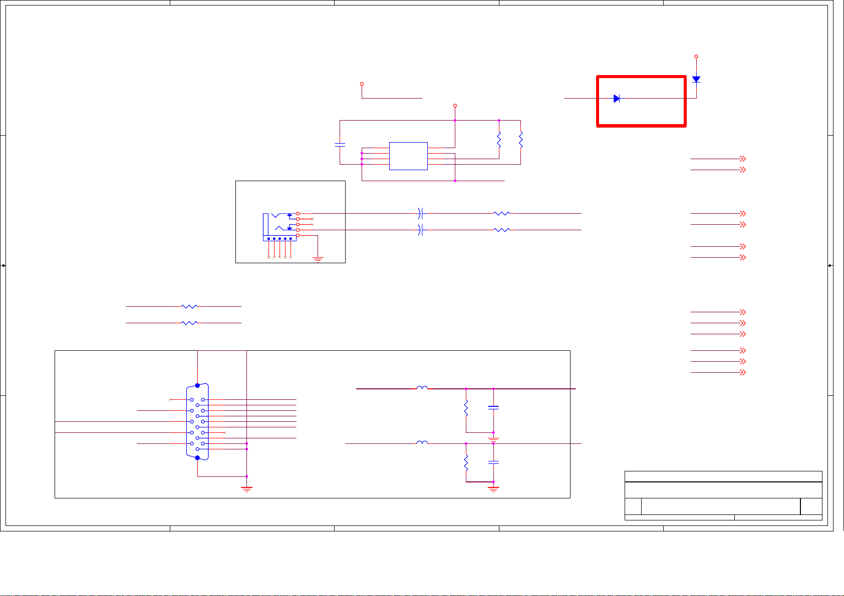
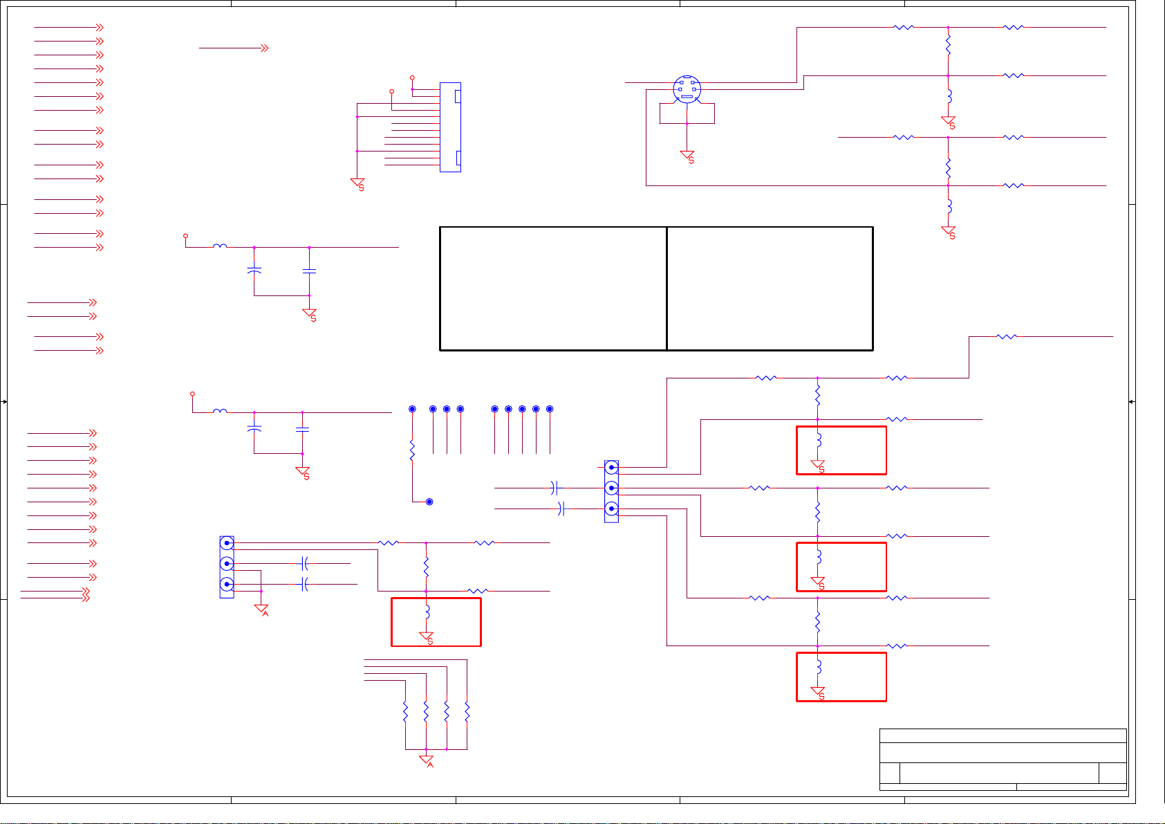
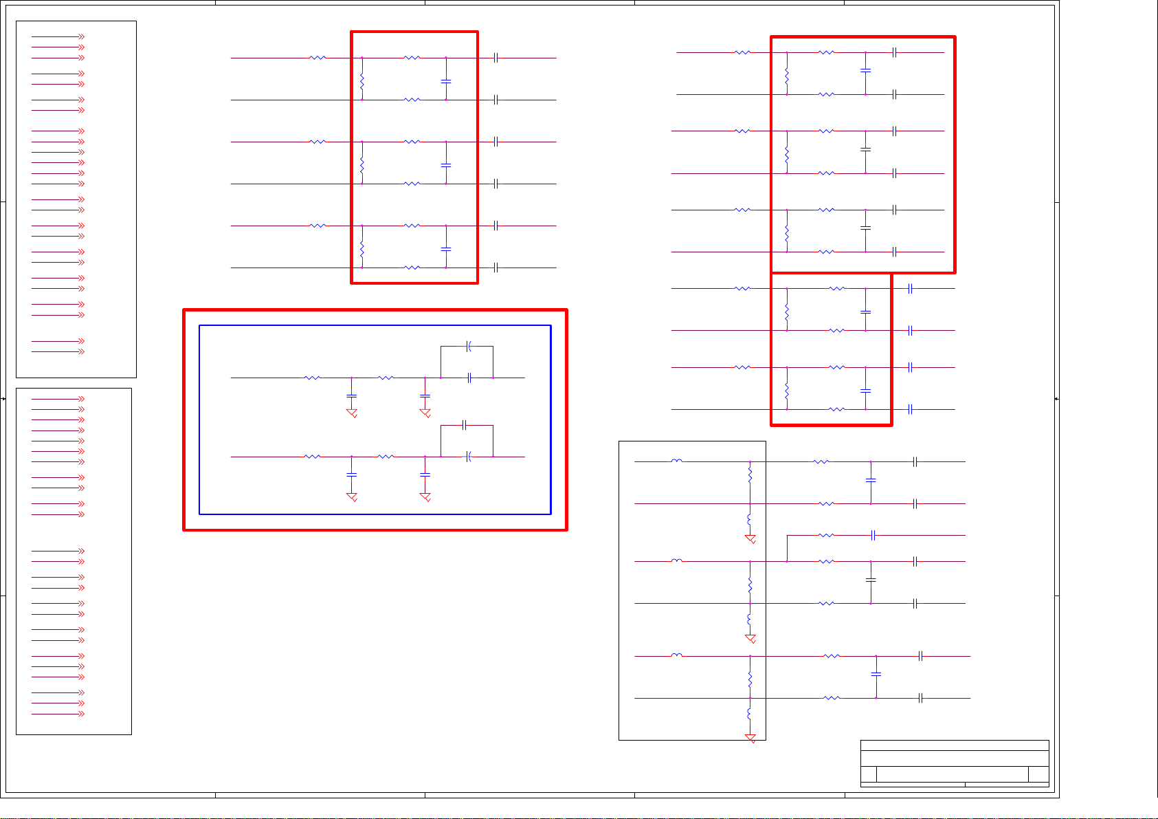
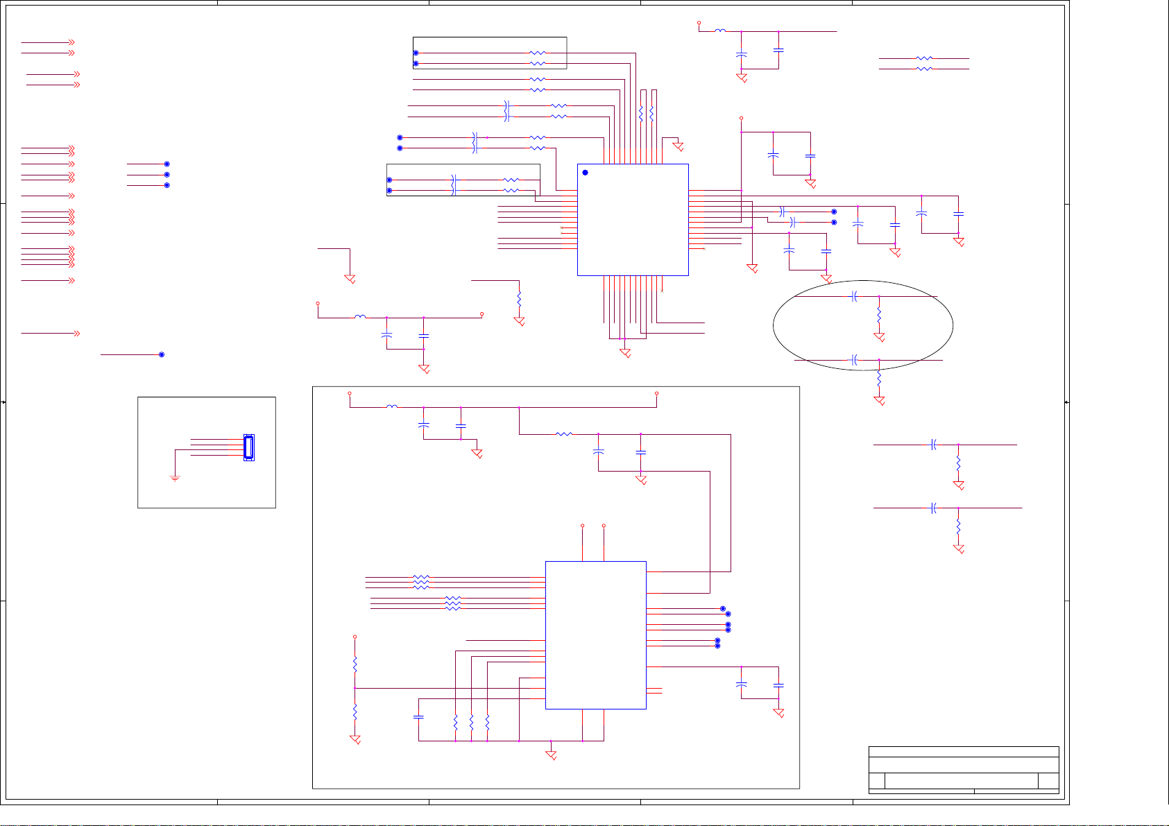
Circuit Diagram
Disassembly
Pin Descriptions
LCD Panel specification
Exploded View Diagram
Spare parts list
V-chip password and software upgrade
This manual is the latest at the time of printing, and does not
include the modification which may be made after the printing,
by the constant improvement of product.
Page 2
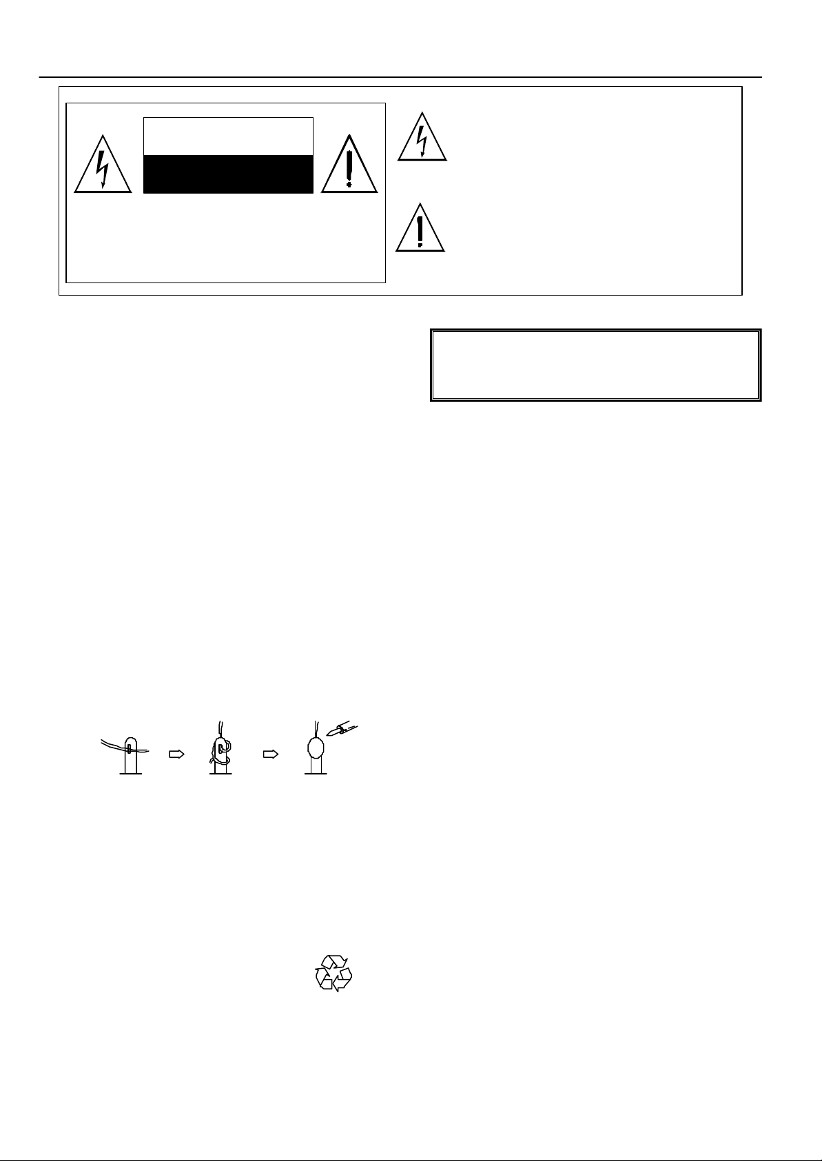
I. Safety Instru ctions
CAUTION
RISK OF ELECTRIC SHOCK
DO NO T OPEN
The l ightning fla sh w ith arro whead symb ol,
within an equilateral triangle, is intended to alert
the user to the presence of uninsulated “dangerous
voltage” within the product’ s enclosure that may
be of sufficient magnitude to constitute a risk of
electric shock to persons.
CAUTIO N: TO REDUCE THE RISK OF ELECTRIC
SHO CK, DO NOT REMOVE COVER (OR BACK). NO
USER-SERVI CEABLE PART S INSIDE. REFER
SERVICING TO QUALIFI ED SERVICE PERSONNEL
O NLY.
PRECAUTIONS DURING SERVICING
1. In a ddition to safety, other parts and assemblies are
speci fied for conformance with such regulations as
those applyi ng to spurious radiation. These must
also be replaced only with specified replacements.
Exampl es: RF converters, tuner units, antenna
selection switches, RF cables, noise-blocking
capacitors, noise-bl ocking filters, etc.
2. Use sp ecified internal Wiring. Note especially:
1) Wires covered with PVC tubing
2) Do uble insulated wires
3) Hig h voltage leads
3. Use specified i nsulating materials for hazardous
live pa rts. Note especially:
1) In sulating Tape
2) PVC tubing
3) Spa cers (insulating barriers)
4) Insulating sheets for transistors
5) Plastic screws for fixing micro switches
4. When replacing AC primary side compo nents
(tran sformers, power cords, n oise blocking
capacitors, e tc.), wrap ends of wires securely about
the te rminals before soldering.
5. Make sure that w ires do not contact heat generating
parts (he at sinks, oxide metal film resistors, fusible
resistors, etc.)
6. Check if replace d wires do not contact sharply edged
or po inted parts.
7. Make sure that foreign objects (screws, solder
drop lets, etc.) do not remain insi de the set.
MAKE YOUR CONTRIBUTION TO PROTECT THE
ENVIR ONMENT
Used batteries with the ISO symbol
for recycling a s well as small
accumu lators (rechargeable batteries), mini-batteries
(cell s) and starter batteries should not be thrown
into the garbage can.
Please leave them at an appropriate depot.
The excla mation po int wi thin a n equilateral
tri angle is intended to a lert th e user to the
presence of important operating and maintenance
(servici n g) instr u ct i o n s i n th e liter a tu re
accompanying the appliance.
W ARNING:
Before servicing this TV receiver, read the X-RAY
RADIATION PRECAUTION, SAFETY INSTRUCTION
and PRODUCT SAFETY NOTICE.
X-RA Y RADIATION PRECAUTION
1. Excessively high can prod uce potentially hazardous
X-RAY RADIATION. T o avoid such hazards, the high
volta ge must not exceed the specified limit. The
normal va lue of the high voltage of this TV receiver
is 2 7 KV at zero bean current (minimum brightness).
The high voltage must not exceed 30 KV under any
circu mstances. Each time when a re ceiver requires
servici ng, the high voltage should be checked. The
readi ng of the high voltage is re commended to be
reco rded as a part of the service record, It is
important to u se an accurate and reliable high
voltage meter.
2. The only source of X-RAY RADIATION in this TV
receiver is the picture tube. For con tinued X-RAY
RADIATION protectio n, the replacement tube must be
exactly the sa me type as specified in th e parts list.
3. Some parts in this TV receiver have special safety
related characteristics fo r X-RADIATION protection.
For continued safety, the parts replacement should
be under taken only afte r referring the PRODUCT
SAFETY NOTICE.
SAFETY IN STRUCTION
The se rvice should not be attempted by anyone
unfamiliar with the ne cessary instructions on this TV
receiver. The fo llowing are the necessary instructions
to be ob served before servicing.
1. An isolation transformer shoul d be connected in the
power li ne between the receiver and the AC line
when a service is performed on the primary of the
conve rter transformer of the set.
2. Comply wi th all caution and safety related provided
on th e back of the cabinet, inside the cabinet, on the
chassis or p icture tube.
3. T o avoid a shock hazard, always discharge the
pictu re tube's anode to the chassis g round before
removi ng the anode cap.
- 2 -
Page 3
4. Completely discharge the high potential voltage of the
picture tube before handli ng. The picture tube is a
vacuum and if bro ken, the glass will explode.
5. When rep lacing a MAIN PCB in the cabinet, always
be certai n that all protective are installed properly
such as control knobs, adjustment co vers or shields,
barri ers, isolation resistor networks etc.
6. When se rvicing is required, observe the original lead
dressing. Extra precau tion should be given to assure
correct lead dressing in the high voltage area.
7. Keep wires away from high voltage or high te mpera
ture components.
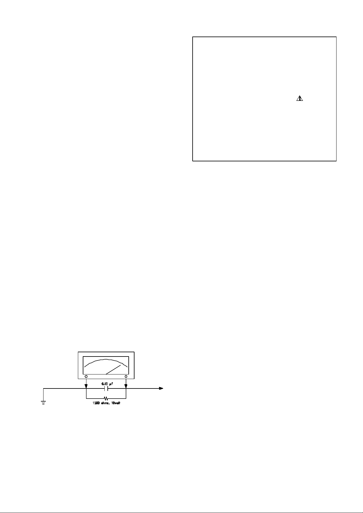
8. Befo re returning the set to the customer, al ways
perform an AC leaka ge current check on the exposed
meta llic parts of the cabinet, such as anten nas,
termin als, screwheads, metal overlay, control shafts,
etc., to be sure the set is safe to operate without
danger of electrica l shock. Plug the AC line cord
directly to the AC outlet (do not use a line isolation
transformer d uring this check). Use an AC voltmeter
havin g 5K ohms volt sensitivity or more in the
following manner.
Conne ct a 1.5K ohm 10 watt resistor paralleled by a
0.15µF AC type capacitor, between a good earth
ground (water pipe, conductor etc.,) and the exposed
metallic parts, one at a time.
Measure the AC vol tage across the combination of
the 1 .5K ohm resistor and 0.15 uF capacitor. Reverse
the AC p lug at the AC outlet and repeat the AC
volta ge measurements for each exposed metallic
part.
The me asured voltage must not exceed 0.3V RMS.
This correspo nds to 0.5mA AC. Any value exceeding
this limit constitutes a potential shock hazard and
must be corrected immediately.
The resistance measurement should be done
betwe en accessible exposed metal parts and power
cord plug prongs with the power switch "ON". The
resi stance should be more than 6M ohms.
PRODUCT SA FETY NOTICE
Many e lectrical and mechanical parts in this TV
receiver have special safety-related characteristics.
These characteristics are offer passed unnoticed by
visual spection and the protection afforded by them
cannot necessari ly be obtained by using replacement
compon ents rates for a higher voltage, wattage, etc.
The replacemen t parts which have these special
safety characteristics are identified by marks on
the schematic diagram and on the parts list.
Before replacin g any of these components, read the
parts list in thi s manual carefully. The use of
substitute re placement parts which do not have the
same safety characteristics as specified in the parts
list may cre ate shock, fire, X-RAY RADIATION or
other h azards.
Good earth ground
such as the water
pipe, conductor,
etc.
AC Leak age Current Check
AC VOLTMETER
Place this probe
on eac h e xpos ed metallic
part
- 3 -
Page 4

KAWA ELECTRONIC RESEARCH & DEVELOPMENT CENTRE
Product Specification
Reference No. : LC27HAB002
Revision : 0
Date : 2005.08.1
Page : P.1 of 8
Model No. : LC27HAB
Customer Model No. : LCT2715
Design Code : LC27HABCUSXM1-A01
BOM No. : LC27HABCUSXM1-A01
Artwork Ass'y No. : 580-L26ABHM-TU02L
Description : AKAL LCD TV 26” NTSC AC100V-240 V AC USA
Checked By: Electronic Engineer
Mechanical Engineer
Approved By: Engineering Manager
Approved By: PM Department Head
DOC Rev
NO.
0 Initial Release
The Latest Revision Details DATE
Page 5
KAWA ELECTRONIC RESEARCH & DEVELOPMENT CENTRE
Reference No : LC27HAB001
Revision : 0
Date : 2005.8.1
Page : P. 2 of 8
General Description
1. Main features
Production Description
Panel Supplier and Model
Chips Solution
Market
1.1 VIDEO SECTION
Display size 27”/16:9
Display Resolution 1366 X 768
Pixel Pitch
Peak Brightness 550(nits)
Contract Ratio 1000:1, Typical (1/100 White Window, Dark Room)
View Angle Hor. And Vert. ≥170 degree
Color Deeps 16.7M Color (R / G/ B each 256 Scales)
PC Resolution Supporting VGA, SVGA, XGA,WXGA
HDTV Compatible 480p / 720p / 1080i
Progressive Scanning Yes
Film Mode Pull Down Yes
“GAMMA” Correction Yes
Color Temperature Control Yes
Comb Filter Yes
Second De-interlace for Sub picture No
Wide Mode
TV System NTSC M
Dual Tuner System No
AV Input Color System PAL /NTSC
PIP Basic mode (video on graphic mode,resolution≥1024×768)
AKAL LCD TV 27” NTSC AC100V-240VAC USA
CHIMEI V270B1-L01
MK8205
USA
0.1460mm×0.4365mm
Full,Fill Aspect Ratio,Nonliner,LB to 16:9,
LB subtitles to 16:9 or Anamorphic
1.2 AUDIO SECTION
Audio Output Power 6W×2 Max.(8 ohm)
Sound Effect NO
Tone Control Yes
1.3 Input Terminals
1.4 Output Terminals Audio Output (RCA ; L&R Type) ×1
1.5 Others
Closed Caption / V-Chip Yes
Teletext No
OSD Language English, FranÇais, Español
D-Sub 15 Pin Type(
D-Sub 9 Pin (RS-233 Input ) ×1
Component Video-YPbPr/YCbCr ×2 RCA Terminals
S-Video Input (Mini Din 4Pin) ×1
Video Input RCA Terminals
Y / Pb / Pr, Y / Cb / Cr (RCA Type) ×2
Stereo Audio Input for YPbPr / YCbCr x 2
Analog-RGB Input ) ×1
(3.5mm Phone Type) ×1
Page 6
KAWA ELECTRONIC RESEARCH & DEVELOPMENT CENTRE
Reference No : LC27HAB001
Revision : 0
Date : 2005.8.1
Page : P. 3 of 8
Stereo Decode
Power Rating AC 100-240V, 50/60Hz
Power Consumption 200W
1.6 Support the Signal Mode
This machine can support the different from VGA signal mode in 19 kinds
No Resolution
1) 640×480 31.50 60.00 25.18
2) 640×480 35.00 67.00 30.24
3) 640×480 37.50 75.00 31.50
4) 640×480 37.86 72.81 31.50
5)
6) 800×600 35.16 56.25 36.00
7) 800×600 37.90 60.32 40.00
8) 800×600 46.90 75.00 49.50
9) 800×600 48.08 72.19 50.00
10) 832×624 49.00 75.00 57.27
11) 1024×768 48.40 60.00 65.00
12) 1024×768 56.50 70.00 75.00
13) 1024×768 60.00 75.00 78.75
14) 1152×864 63.86 70.02 94.51
15) 1152×864 67.52 75.02 108.03
16) 1280×960 60.02 60.02 108.04
17) 1280×1024 64.00 60.01 108.00
MTS with SAP
Horizontal
Frequency(Hz)
720×400
31.47 70.08 28.32
Vertical
Frequency(KHz)
Dot Clock
Frequency(MHz)
1.7 HDTV Mode (YPbPr)
No Resolution
1) 480i 15.734 59.94 13.50
2)
3)
4)
5)
6)
480p(720×480)
576p(720×576)
720p(1280×720)
720p(1280×720)
1080i(1920×1080)
Horizontal
Frequency(KHz)
31.468 59.94 27.00
31.25 50.00 27.00
37.50 50.00 74.25
45.00 60.00 74.25
33.75 60.00 74.25
Vertical
Frequency(Hz)
Dot Clock
Frequency(MHz)
Page 7
KAWA ELECTRONIC RESEARCH & DEVELOPMENT CENTRE
Reference No : LC27HAB001
Revision : 0
Date : 2005.8.1
Page : P. 4 of 8
2. LCD local control button
3. Led indicators :
4. OSD language
5. OSD Full on screen display
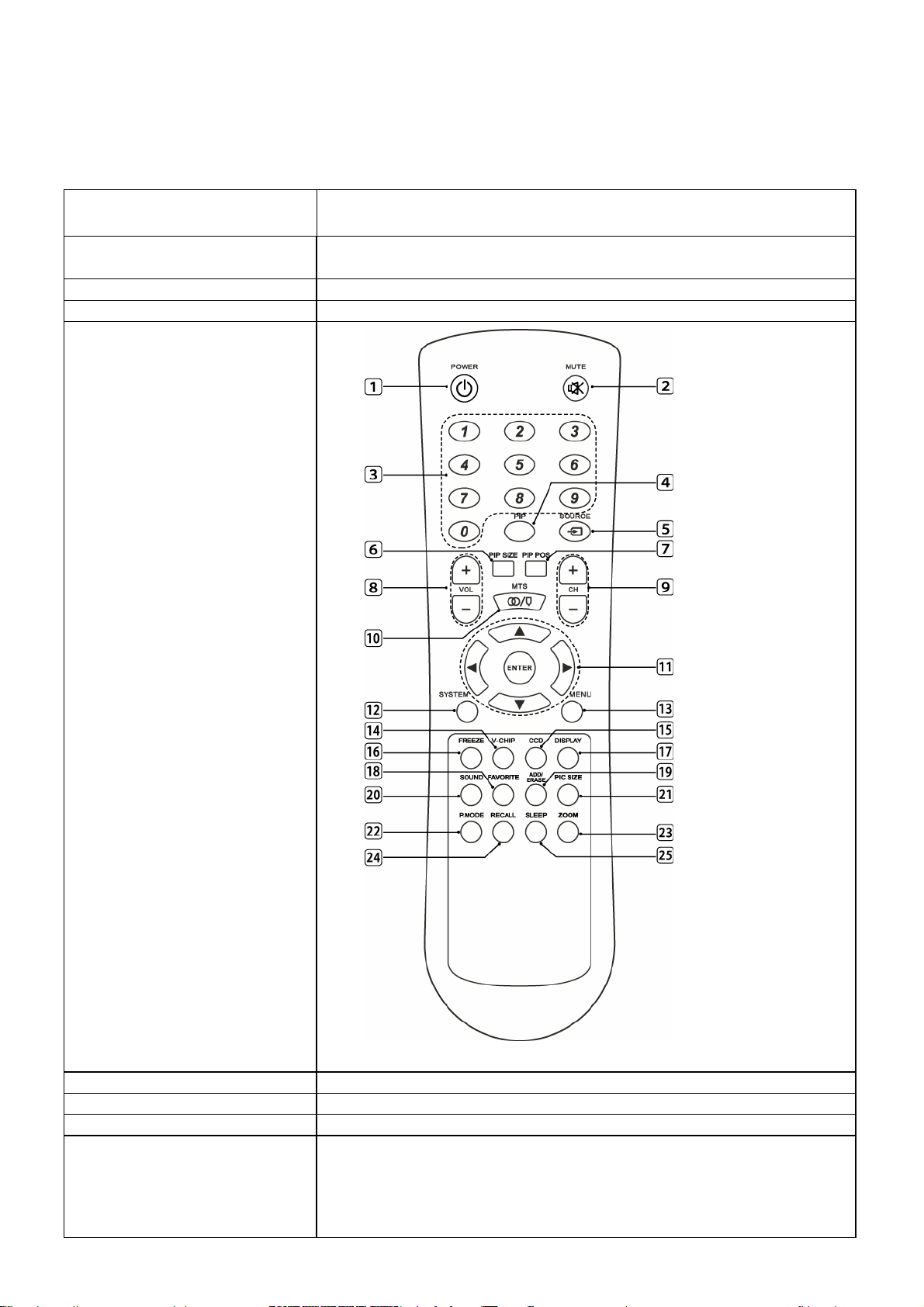
6. Remote control unit
Customer Remote
Code: 609F(NEC)
1 POWER button
2 MUTE button
3 0-9 DIGITAL button
4 PIP button
SOURCE
5
6 PIP SIZE button
7 PIP POS button
8 VOL +/- button
9 CH +/- button
10 MTS button
11 UP/DOWN,LEFT/RIGHT
ENTER buttons
12 SYSTEM button
13 MENU button
14 V-CHIP button
15 CCD button
16 FREEZE button
17 DISPLAY
18 FAVORITE button
19 ADD/ERASE buttons
20 SOUND button
21 PIC SIZE button
22 P.MODE button
23 ZOOM button
24 RECALL button
SLEEP button
25
button
buttons
Main power : push switch
Channel +/- volume up/down menu input. standby : soft touch
Power on: Green
Standby: Red
English, FranÇais, Español
7. Safety standard UL/FCC/cUL
8. EMC standard 15 Parts of the FCC rules,CLASS B
9. Performance standard LCD-TV Standard
10. Accessories Battery 2pcs
User Manual 1pcs
AC Cable 1pcs
Remote Control 1pcs
The Accessories box 1pcs
E7501-051001
Page 8
KAWA ELECTRONIC RESEARCH & DEVELOPMENT CENTRE
Reference No : LC27HAB001
Revision : 0
Date : 2005.8.1
Page : P. 5 of 8
Technical Data
1. Chassis MICO
TV AC 100-240 V, 50/60Hz 2. Power supply
Remote controller Battery 3V (UM-4/R03/AAA×2)
RF input NTSC M 3. TV system
Video input PAL/NTSC 3.58/NTSC 4.43
4. Receiving channels
TV
CATV 1~125CH
VHF-L : 2~6CH
VHF-H : 7~13CH
UHF : 14~69CH
5. Intermediate
frequencies
6. Sca nn in g H or iz o ntal (Hz ) 15625/15750
7. AC plug UL Plug
8. Panel V270B1-L01
9. Speaker Internal 8 ohm 10W (max) ×2
10.Operating
temperature
Accept picture/sound
11. Operating relative
humidity
Accept picture/sound
12. Electrical &
optical
specification
13. Circuit diagram
drawing No.
15. Cabinet
16. Cabinet color
17. Packing 1 set per
18. Container stuffing
method
19. Dimension (mm) LCD-TV
(No packing)
Remote control unit
20. Net weight LCD-TV 14.1Kg (with Stand) approx.
Remote controller 70g (approx.)
Picture 45.75MHz
Ver ti ca l ( Hz ) 50/60
Fulfill all specifications
reproduction
Fulfill all specifications 45% ~ 75%
reproduction
See the attachment 1.
RD/05/P/LC26HAB/CSI/02 REV: 01
15°C ~ 30°C
5°C ~ 33°C
20% ~ 80%
LC26HAB
883(W) × 468(H) × 110(D)mm (w/o Stand)
883(W) × 523(H) × 250(D)mm (with Stand)
183(L) × 53(W) ×28(T)mm
21. Cell Defect Subject to Panel supplier specification
Page 9
KAWA ELECTRONIC RESEARCH & DEVELOPMENT CENTRE
Reference No : LC27HAB001
Revision : 0
Date : 2005.8.1
Page : P. 6 of 8
Attachment 1:Electrical & Optical Specification
No. Items Instruction Typical Limit Unit
1 Video sensitivity For 30dB S/N 44 ≤51 dBuV
2 FM sound sensitivity For 30dB S/N 21 ≤35 dBuV
3 Color sensitivity For RF transmission 37 ≤40 dBuV
4 CCD sensitivity
5 Minimum NICAM threshold Without crackline noise N/A N/A dBuV
6 Stereo Channel Separation BTSC. 18 ≥15 dB
TV screen refreshes 40 times
number of mistakes≤8
43 ≤50 dBuV
AGC static characteristic
7
8 Selectivity Adjacent sound carrier 30 ≥28
Below adjacent sound carrier 30 ≥30 dB
Adjacent picture carrier 45 ≥40
Up adjacent picture carrier 40 ≥30
9 IF rejection 55 ≥45 dB
10 Image rejection VHF 57 ≥45 dB
UHF 55 ≥40
11 AFT pull-in range ±1.0 ≥⏐±1.0⏐ MHz
12 Chroma sync pull-in range ±500 ≥⏐±200⏐ Hz
13 Color killer function -11 ≤-10 dB
14 Resolution
Video
Accept. Picture/Sound repr. 90
RF
Vertical
Horizontal
Vertical 400 ≥400 Lines
PAL 300 ≥300 Lines Horizontal
NTSC 260 ≥240 Lines
PAL 410 ≥400 Lines
NTSC 320 ≥300 Lines
450 ≥450 Lines
≥90
dBuV
White
Coordination
16 View
Angle(Lo/3)
17 Overscan Cross hatch signal 96 94~98 %
Horizontal
Vertical
XW 0.295 0.295±0.02 15 Color
W
Y
Full Pattern
0.300 0.300±0.02
170
≥170
Degree
18 Picture position In all direction ±2 ≤⏐±3⏐ mm
19 H sync pull-in range ±400 ≥⏐±200⏐ Hz
20 V sync pull-in range 6 ≥6 Hz
21 Audio frequency response ±3dB ref. to 1KHz 0.15~12 0.2~12 KHz
Page 10
KAWA ELECTRONIC RESEARCH & DEVELOPMENT CENTRE
Reference No : LC27HAB001
Revision : 0
Date : 2005.8.1
Page : P. 7 of 8
22
Max Audio Output Power 7×2 ≥5.0×2 W
23 Audio output power
10% THD
24 THD Po=0.5W 0.5 ≤3 %
25 Signal to buzz ratio coeighting 50 ≥30 dB
26 Minimum volume hum coeighting 6 ≤10 mVrms
27 Maximum woofer output power N/A N/A W
28 Woofer audio frequency
response
29 Tone low frequency 100Hz ref. to 1KHz
30 Tone high frequency 10KHz ref. to 1KHz
31 Balance Center 0 ≤⏐±2⏐
Max. 3 >2 dB
Min. -35 ≤-30
32 Video input level 1.0 1±0.3 Vpp
1KHz 10% THD 6×2
±3dB ref. to 15Hz AV
mode
AV mode
AV mode
N/A N/A Hz
±8 ≥⏐±3⏐ dB
±8 ≥⏐±3⏐ dB
≥4.0×2 W
33 Audio input level*(1) 1.0 * 0.5±0.3 Vrms
34 Video output level N/A N/A Vrms
35 Audio output level*(2) 0.3 * 0.5±0.3 Vrms
36 AV Audio input max. level 2 ≤2 Vrms
37 AV Audio output L/R
Separation
39 IR receiving distance 0 Degree 7 ≥6 m
IR receiving
angle
41 Dielectric strength DC 3KV 1min. 5 ≤10 mArms
42 The vibration noise from
electromagnetic devices in LCD-
TV set
left/right 60 ≥45 Degree40
Up/down
35 ≥30 dB
Operating 200 ≤200 W 38 Power consumpution
Stand by 3 ≤5 W
5m
The distance between
the tester and the
LCD-TV set is four
times as many as the
screen height
20 ≥15 Degree
No obvious vibration noise can be
heard
Page 11
KAWA ELECTRONIC RESEARCH & DEVELOPMENT CENTRE
Reference No : LC27HAB001
Revision : 0
Date : 2005.8.1
Page : P. 8of 8
Test Condition
All tests shall be performed under the following conditions unless otherwise specified
1 Picture Modulation 87.5%
2 Sound Modulation
3 Picture to Sound Ratio 10dB
4 Sound Artificial Load
Resistor
Video signal
5
6 Audio signal 1KHz sine wave 0.5Vrms
7 Other conditions:
A. Switch LCD-TV on and let it warm up for more than 30 minutes.
Viewing distance: 3H (H: Panel High) in front of LCD, about 2M.
Ambient light: ≤0.1 cd/ m
B. Brightness, Contrast, Saturation, Tint, sharpness set at normal.
C. Connect RMS volt meter to speaker terminals and adjust the LCD volume to get 500mW RMS
power at each terminals.
D. With image sticking protection of LCD module. The luminance will descend by time on a same
still screen and rapidly go down in 5 minutes, when measuring the color tracking and luminance
of a same still screen, be sure to accomplish the measurement in one minute to ensure its
accuracy.
E. Due to the structure of LCD module. The extra-high-bright same screen should not hold over 5
minutes for fear of branding on the panel.
F. RF test point: Video output.
27KHz Dev. For DK/I/BG
15KHz Dev. For M/N
8 ohm
Stair and Special
2
8 Note:
*(1) Now this project cannot fit the limited spec. the typical audio input level is 1.0 Vrms,
*(2) The audio out level is controlled by the volume level, the range is from 0 to 0.5Vrms.
Page 12
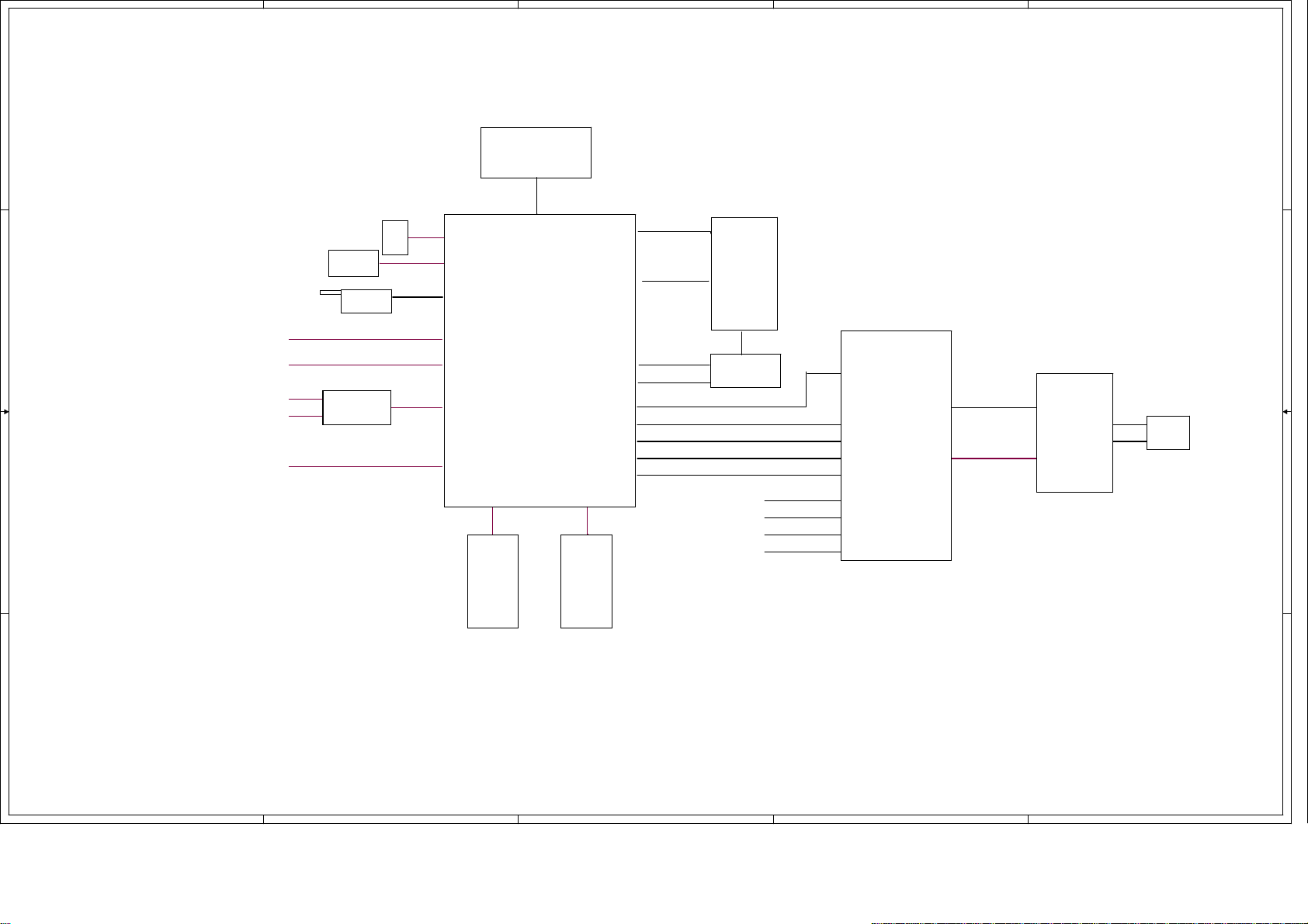
A
4 4
B
C
D
E
Flash
IR
Keypad
TV
3 3
Tuner
LVDS SIGNAL
LVDS SIGNAL
LVDS PANEL
AV1
S_Video
Y1PbPr
Y2PbPr
VGA
MUX
YPbPr
MT8205
GPIO
GPIO
AOSDATA1
DACBCLK
DACMCLK
DACLRC
DOUT
Backlight
WM8776
COD_VOUTR
COD_VOUTL
Audio Board
Speaker
VGA_L/R
2 2
S1_AV1_L/R
Y1PbPr_L/R
Y2PbPr_L/R
DDR1 DDR2
1 1
A
B
C
D
E
Page 13
A
MT8205P1V3.2
MT8205E (PBGA388) LCDTV BOARD 4 LAYERS
1. INDEX
4 4
2. LDO
3. MT8205E PBGA388
B
C
D
E
Rev DateP#History
V0.1 2004/11/29
V0.2 1. 2.5V use 5VSB conversion. All 0402 change to 0603
1.FIRST VERSION
2. LED_RED/GRN CIRCUIT CHANGE
3. Change Power on/off circuit(ORO7 CTRL PIN)
4. WM8776 DVDD Needed
5. Del the Si9936 LVDS Parts
6. Del DVI&AD9883 PARTS
2005/03/09
4. MT8205 ANALOG DECOUPLING
5. MT8205 DIGITAL DECOUPLING
6. ICE I/F
7. DDR MEMORY & FLASH
8. DVI INPUT
9. AD9883
10. VGA IN & PC AUDIO IN
11. VIDEO IN & TUNER I/O
J24
12. AUDIO / VIDEO IN CIRCUIT
13. WM8776 AUDIO CODEC
3 3
2 2
1 1
14. LVDS / CRT / TTL OUT
15 BACK LIGHT / KEYPAD
16. READER CARD I/F
HOLE/GND
H1
9
9
8
8
7
7
6
6
9
9
8
8
7
7
6
6
9
8
7
6
9
8
7
6
2
2
3
3
4
4
5
5
1
1
HOLE/GND
H2
2
2
3
3
4
4
5
5
1
1
HOLE/GND
H3
9
8
7
6
9
8
7
6
2
2
3
3
4
4
5
5
1
1
HOLE/GND
H4
2
2
3
3
4
4
5
5
1
1
H5
9
9
8
8
7
7
6
6
1
H6
9
9
8
8
7
7
6
6
1
UP3_0 BLACKLIGHT ON/OFF
MUTE<-->UP1_5
HOLE/GND
2
2
3
3
4
4
5
5
1
HOLE/GND
2
2
3
3
4
4
5
5
1
P5
CONNECTOR DB9
1
6
2
7
3
8
4
9
5
RxD
TxD
RS-232
R51
10k
RSRXD
RSTXD
C1 0.1uF
C3 0.1uF
C6 0.1uF
C7 0.1uF
DIP8/P2.0
TO Power BD
24V
INVERTER_PWR
PWR_GND
DV33A
R52
J2
10k
1
2
3
4
4x1 W/HOUSING
DIP4/W/H/P2.0
U6
13
R1IN
8
R2IN
11
T1IN
10
T2IN
1
C+
3
C1-
4
C2+
5
C2-
2
V+
6
V-
MAX232A
R1OUT
R2OUT
T1OUT
T2OUT
12
9
14
7
5VSB
16
VCC
GND
C8
0.1uF
15
VCC
1
2
3
4
5
6
7
8
TXD
RXD
J108
1
2
3
4
5
6
8x1 W/HOUSING
DIP8/W/H/P2.54
TXD
RXD
+12V
J6
5
4
3
2
1
5x1 W/HOUSING
DIP5/W/H/P2.0
SYS_PWR
5VSB
+12V
5VSB
+
CB75
0.1uF
+
5VSB
5VSB
3 2
CE16
220uF/16v
C220UF16V/D6H11
CE93
220uF/16v
C220UF16V/D6H11
SYSTEM EEPROM
1
2
3
4 5
R359
10k
Q14
1
SOT23/SMD
2N3904
L14
FB
BEAD/SMD/0805
U13
NC
NC
NC
GND SDA
EEPROM 24C16
SOP8/SMD
ORO7 High :POWER OFF
ORO7 LOW :POWER ON
R364
ORO7
4.7k
For Tuner
CE17
+
47uF/16v
8
VCC
7
WP
SCL
SCL
6
SDA
5VSB
R53
10k
TUNER_12V
CB11
0.1uF
R54
10k
FOR Tuner
TXD
RXD
SCL
SDA
+12V
TUNER_12V
ORO7
MUTE
TXD 3
RXD 3
SCL 6,9,11,13
SDA 6,9,11,13
+12V 2
TUNER_12V 11
ORO7 3
UP1_5 6
Title
AUIO IN/OUT GND ANALOG INPUT GND
A
B
DIGITAL GND
C
D
LCD TV - MediaTek MT8205 Solution
Size Doc Number Rev
C
Date: Sheet of
INDEX
E
116Tuesday, May 10, 2005
V0.1
Page 14
A
B
C
D
E
Power ON alive source
Vout
4 4
VCC
+
CE4
220uF/16v
CB4
0.1uF
U1
OUTIN
SOT223/SMD
ADJ/GND
CM1117-3.3V
1
23
L8
FB
BEAD/SMD/0805
+
CE5
220uF/16v
DV33
CB5
0.1uF
DV33
5VSB
CE6
220uF/16v
U35
M1117-3.3V
+
CB200
0.1uF
OUTIN
SOT223/SMD
ADJ/GND
1
23
CE118
+
220uF/16v
BEAD/SMD/0805
CB201
0.1uF
L7
FB
DV33A
ADJ/GND
U5
ADJ/GND
U3
CM1117-3.3V
1
23
OUTIN
3 3
SOT223/SMD
L11
FB
BEAD/SMD/0805
+
CE10
220uF/16v
C5
10uF/10v
1.25x(1+180/110)=3.3V
AV33
CB6
0.1uF
AV33
+
CE11
100uF/16v
CB7
0.1uF
CM1117-1.8V
OUTIN
SOT223/SMD
1
23
+
CE12
220uF/16v
1.25x(1+300/680)=1.8V
L6
FB
BEAD/SMD/0805
CB8
0.1uF
Vout
DV18A
DV33A
DV18A
5VSB
+
+
CE128
220uF/16v
2 2
VCC
+
CE8
100uF/16v
C100UF16V/D6H11
5V ==> +12v
L107
R3 0
FB
R0805/SMD
R5
10
R0805/SMD
L9
12
CHOKE-100uH L18W10H18
L/CHOKE/DIP/1810
U2
SOIC8
8
DRC
7
Ipk
6
VCC
AZ34063A-PWM
L10
+12V
D2
DIODE SMD
1N4148/SMD
R6
13k
C2
CE7
+
1
SWC
2
SWE
3
TC
45
GNDCII
C4
100pF
100uF/16v
270pF
R8
1.5k
R325
FB
0
+12V
+
CE107
100uF/25v/NC
CE129
220uF/16v
CB212
0.1uF
CB213
0.1uF
CB214
0.1uF
CB215
3300pF
CB216
3300pF
CB217
3300pF
1 1
Title
LCD TV - MediaTek MT8205 Solution
Size Doc Number Rev
C
A
B
C
D
Date: Sheet of
LDO
216Tuesday, May 10, 2005
E
V0.1
Page 15
A
XTALI
XTALO
ANALOGVDD
4 4
ADCVDD
APLLVDD
VPLLVDD
ADCPLLVDD1
ADCPLLVDD
AUXTOP
AUXBOTTOM
REXTA
APLL_CAP
PWM2VREF
ADCVDD0
3 3
AVCM
VOCM
VICM
VREFP4
VREFN4
DACFS
DACVREF
DACVDD
LVDDA
2 2
IR
1 1
XTALI 4
XTALO 4
ANALOGVDD 4
ADCVDD 4
APLLVDD 4
VPLLVDD 4
ADCPLLVDD1 4
ADCPLLVDD 4
AUXTOP 4
AUXBOTTOM 4
REXTA 4
APLL_CAP 4
PWM2VREF 4
ADCVDD0 4
AVCM 4
VOCM 4
VICM 4
VREFP4 4
VREFN4 4
DACFS 4
DACVREF 4
DACVDD 4
LVDDA 4
IR 15
DV33A
GND
DV18A
GND
U7
ADCVDD0
ADCVDD0
MPX1
MPX2
GND
VREFP4
VREFN4
GND
ADCVDD
PWM2VREF
AUXTOP
AUXBOTTOM
GND
VPLLVDD
VPLLVDD
GND
GND
REXTA
VPLLVDD
LVDDA
AP7
AN7
CLK2+
CLK2GND
AP6
AN6
AP5
AN5
LVDDA
AP4
AN4
AP3
AN3
GND
CLK1+
CLK1AP2
AN2
LVDDA
AP1
AN1
AP0
AN0
GND
DACVDD
DACVREF
DACFS
GND
SVM
DACVDD
GND
DACVDD
G
GND
B
R
VSYNC
HSYNC
OBO7
OBO6
OBO5
AC18
L11
M12
M11
N12
N11
AC9
P11
AA1
AA2
AA3
AA4
AB1
AB2
AB3
AB4
AC1
AC2
AC3
AC4
R11
AD1
AD2
AD3
AD4
AE1
C3
D3
C1
C2
D1
D2
F2
D4
E1
E2
E3
E4
F1
F4
F3
G3
J3
G4
H3
K3
K4
J4
H4
L3
G2
G1
H2
H1
J2
J1
K2
K1
L4
L2
L1
M2
M1
N2
N1
P2
P1
M3
R2
R1
T2
T1
N3
M4
N4
T4
P3
R3
P4
U4
R4
U3
V4
T3
U1
U2
V1
V2
V3
W1
W2
W3
W4
Y1
Y3
Y4
VFEVDD1
ADCVDD4
SIF
AF
ADCVSS4
REFP4
REFN4
ADCVSS
ADIN4
ADIN3
ADIN2
ADIN1
ADIN0
ADCVDD
PWM2VREF
AUXVTOP
AUXVBOTTOM
VPLLVSS
VPLLVDD
DLLVDD
DLLVSS
BGVSS
REXTA
BGVDD
LVDDA
A7P
A7N
CLK2P
CLK2N
LVSSA
A6P
A6N
A5P
A5N
LVDDB
A4P
A4N
A3P
A3N
LVSSB
CLK1P
CLK1N
A2P
A2N
LVDDC
A1P
A1N
A0P
A0N
LVSSC
DACVDDC
VREF
FS
DACVSSC
SVM
DACVDDB
DACVSSB
DACVDDA
G
DACVSSA
B
R
DE
VSYNCO
HSYNCO
VCLK
EBO7
EBO6
EBO5
EBO4
DVDD3I
EBO3
EBO2
EBO1
EBO0
EGO7
DVSS18
EGO6
EGO5
EGO4
EGO3
EGO2
EGO1
EGO0
ERO7
ERO6
ERO5
DVDD18
ERO4
ERO3
ERO2
DVSS3
ERO1
ERO0
OBO7
OBO6
OBO5
GND
AVCM
L12
AVCM
VFEVSS1
OBO4
OBO3
AE2
AF1
OBO3
OBO4
ADCVDD0
CVBS2+
CVBS2-
CVBS2P
CVBS2N
ADCVDD0
OBO1
OBO0
OBO2
AE3
AF3
AF2Y2AF4
OBO1
OBO2
OBO0
CVBS1+
CVBS1-
CVBS1N
OGO7
AE4
OGO6
OGO7
CVBS0-
CVBS1P
CVBS0N
OGO5
OGO6
AC5
OGO5
CVBS0+
GND
CVBS0P
DVSS18
T11
AD5
OGO4
GND
REFP0
REFN0
ADCVSS0
OGO4
OGO3
OGO2
AE5
AF5
OGO2
OGO3
SC-
ADCVDD0
ADCVDD1
OGO1
AC6
AD9
OGO1
DV33A
SC+
SCP
SCN
DVDD3
OGO0
AD6
OGO0
SY-
AE6
ORO7
SY+
SYN
ORO7
ORO6
AF6
GND
M13A6B6A5B5C5A4B4L13A3B3A2B2A1B1C4D5
SYP
ORO6
AC7
ORO5
REFP1
ADCVSS1
ORO4
ORO5
AD18
AD7
ORO4
DV18A
B
VOCM
ADCVDD0
REFN1
VFEVDD0
DVDD18
ORO3
AE7
AF7
ORO2
ORO3
GND
VOCM
ORO2
AC8
ORO1
VICM
ADCVDD0
C7A7N13B7D7C6D6
VICM
VFEVSS0
ADCVDD2
ORO1
ORO0
HIGHA7
AD8
AF8
ORO0
F_A15
GND
BN
BLUE+
A13
BP
GND
D12
C10
REFP3
ADCVSS3
VGAVSYNC#
VGAHSYNC#
C14
C13
C12
REFN3
VSYNC
N14
DVSS
HSYNC
DV18A
D14
DVDD
CB+
CB-
CR-
CR+
A8B8A9B9C8
CRP
CBN
CRN
GREEN-
GREEN+
BLUE-
VGASOG
ADCVDD0
RED+
RED-
GND
Y+
Y-
SOY
B13
D13
A12
B12
A11
B11D8C11
D11C9D9
D10
A10
B10
YP
YN
CBP
SOY
REFP2
REFN2
ADCVSS2
MON0
MON1
ADCVDD3
RP
GP
RN
GN
SOG
MT8205
HIGHA6
HIGHA5
HIGHA4
HIGHA3
HIGHA1
HIGHA0
AD0
AD1
DVDD18
AD2
AD3
AD4
DVSS3
AD7
AD5
IOA0
IOA3
IOA4
IOA5
IOA6
IOA7
DVSS18
HIGHA2
AE9
AF9
AE10
AF10
AD11
AF12
AE15
P12
AC11
F_A8
F_A9
F_A10
F_A12
F_A13
F_D0
F_A11
F_A14
GND
AD15
F_D1
AD6
AC19
AC15
AF16
AE16
R12
AF17
AD16
AD17
AC16
F_D3
F_D6
F_D5
F_D7
F_D4
F_D2
DV18A
IOA0
GND
AD14
IOA1
A16
IOA1
IOA2
AF14
AF13
AE13
AD13
AC13
AE8
AE14
F_A16
IOA7
IOA6
IOA3
IOA5
IOA4
IOA2
ADCPLLVDD
GND
ADCPLLVDD1
GND
M14
C15
D15
L14
ADCPLLVDD
ADCPLLVSS1
ADCPLLVDD1
DVDD3I
A17
IOA18
AC10
AC17
AE12
AD12
F_A17
F_A19
F_A18
DV33A
ANALOGVDD
GND
B14
D16
L15
TESTP
SYSPLLVSS
SYSPLLVDD
ADCPLLVSS
IOA20
DVSS18
IOA21
IOA19
AE11
T12
AF11
F_A20
F_A21
GND
C
XTALO
ANALOGVDD
A14
B15
C16
XTALO
TESTN
XTALVDD
IOALE
IOOE#
IOWR#
AE17
AF15
AC12
F_OE#
IOWR#
XTALI
A15
XTALI
IOCS#
AC14
IOCE#
APLL_CAP
GND
A16
M15
XTALVSS
WR#
AF18
AE18
GND
D18
APLL_CAP
RD#
AD10
DV33A
ANALOGVDD
APLLVDD
C17
D17
APLLVSS
APLLVDD
INT0#
DVDD3
AE19
AF19
8205UP1_2
GND
C18
DMPLLVDD
UP12
AF20
8205UP1_3
VI0
B16
VI0
DMPLLVSS
UP13
UP14
AE20
8205UP1_4
VI1
A17
AD19
DV18A
D
DV33A
DV33A
HWSCL 6
HWSDA 6
TXD 1
RXD 1
IOA[0..7] 6
8205UP3_4 6
8205UP3_5 6
R365
47k
R18
10k
+
CE21
10uF/25v
GND
GND
DV18A
VI8
VI6
VI4
VI5
VI3
VI7
VI2
B17
VI1
DVDD18
AD20
8205UP1_5
VI9
VI13
VI12
VI14
VI15
VI11
VI10
M16
A21
D21
C21
B20
L16
A20
D20
C20
B19
A19
E23
D19
C19
B18
A18
VI9
VI8
VI7
VI6
VI5
VI4
VI3
VI2
DVDD18
UP30
PRST#
UP34
UP17
UP15
UP31
DVSS18
UP16
AE21
AC21
AD22
AF21
AD21
P13
AC20
8205UP3_0
8205UP3_1
8205UP1_7
8205UP1_6
8205UP3_4
URST#
GND
AC22
8205UP3_5
VI15
VI14
VI13
VI12
VI11
VI10
DVSS3
UP35
PWM0
FCICMD
FCICLK
FCIDAT
GPIO0
AE24
AF24
AC23
AD23
AE22
AF22
AF23
AE23
IR
PWM0
PWM1
FCLK
FCMD
RxD
FDAT
GPIO
VI17
VI16
B21
VI16
DVSS18
RXDIRPWM1
TXD
AD24
TxD
GND
C22
R13
VI18
D22
VI18
VI17
ICE
DVSS3
AC24
ICE
VI19
A22
AF25
HWSCL
VI19
SCL
VI20
VI21
B22
VI20
SDA
AE25
VGASCL
HWSDA
VI22
D23
C23
VI21
SCL0
AF26
AE26
VGASDA
VI23
DVIODCK
B23
A23
VI23
VI22
VCLK_DVI
VSYNC_DVI
HSYNC_DVI
AOSDATA0
AOSDATA1
AOSDATA2
AOSDATA3
SDA0
SDA1
SCL1
AB24
AB23
DVISDA
DVISCL
DE_DVI
DVDD18
DVDD3I
AOBCK
AOLRCK
AOMCLK
DVSS3
DQ24
DQ25
DQ26
DVDD2
DQ27
DQ28
DVSS2
DQ29
DVDD2
DQ30
DQ31
DQS3
DQM1
DVSS18
DQS2
DQ23
DQ22
DVSS2
DQ21
DQ20
DVDD18
DQ19
DVDD2
DQ18
DQ17
DQ16
DVSS2
DVSS18
RA11
DVDD2
RCLK
RCLKB
DVSS2
RA10
DVDD2I
DVDD18
RCS#
RAS#
DVSS2
CAS#
RWE#
DQ10
DVDD2
DQ11
DVSS18
DQ12
DQ13
DVSS2
DQ14
DQ15
DQS1
AVSS18
AVDD18
RVREF
DVSS18
DQM0
DQS0
DVDD2
DVSS2
DVDD2
LIN
RA4
RA5
RA6
RA7
RA8
RA9
CKE
RA3
RA2
RA1
RA0
BA1
BA0
DQ8
DQ9
DQ7
DQ6
DQ5
DQ4
DQ3
DQ2
DQ1
DQ0
C24
D24
A24
Y24
A25
A26
B26
F23
B25
B24
C26
C25
E24
N15
G26
G25
F26
F24
F25
E26
N16
E25
G24
D26
D25
H25
H26
P14
J25
J26
K25
P16
K26
L25
AA24
L26
H24
M25
M26
N25
J23
R16
J24
K23
K24
L23
R14
L24
M23
N26
H23
P26
P25
P15
M24
N23
N24
R26
P24
P23
U23
AA23
R24
R23
T24
R15
T23
U24
W26
V25
V26
V23
U25
T13
U26
T25
T15
T26
R25
W25
W23
Y23
G23
T16
Y26
Y25
AA26
V24
AA25
AB26
T14
AB25
AC26
W24
AC25
AD26
AD25
BGA388/SOCKET
MT8205
DVIDE
DVIVSYNC
DVIHSYNC
AOSDATA0
AOSDATA1
AOSDATA2
AOSDATA3
DOUT
DACBCLK
DACLRC
DACMCLK
A_DQ24
A_DQ25
A_DQ26
A_DQ27
A_DQ28
A_DQ29
A_DQ30
A_DQ31
A_DQS3
A_DQM1
A_DQS2
A_DQ23
A_DQ22
A_DQ21
A_DQ20
A_DQ19
A_DQ18
A_DQ17
A_DQ16
A_RA4
A_RA5
A_RA6
A_RA7
A_RA8
A_RA9
A_RA11
A_CKE
A_CLK
A_CLK#
A_RA3
A_RA2
A_RA1
A_RA0
A_RA10
A_BA1
A_BA0
A_CS#
A_RAS#
A_CAS#
A_WE#
A_DQ8
A_DQ9
A_DQ10
A_DQ11
A_DQ12
A_DQ13
A_DQ14
A_DQ15
A_DQS1
VREF
A_DQM0
A_DQS0
A_DQ7
A_DQ6
A_DQ5
A_DQ4
A_DQ3
A_DQ2
A_DQ1
A_DQ0
DV18A
DV33A
SDV25
SDV25
DV18A
SDV25
SDV25
SDV25
DV18A
SDV25
DV18A
SDV25
SDV25
GND
GND
GND
GND
GND
GND
GND
GND
GND
GND
GND
GND
GND
D5
1N4148/SMD
URST#
SW1
123
1=3 2=4
SW4P/DIP/FLAT
GND
DACBCLK
HWSCL
HWSDA
TXD
RXD
IOA[0..7]
8205UP3_4
8205UP3_5
4
E
VI[0..23]
DVIODCK
DVIDE
DVIHSYNC
DVIVSYNC
DVISCL
DVISDA
URST#
A_DQS[0..3]
A_RA[0..11]
A_BA[0..1]
A_DQM[0..1]
A_DQ[0..31]
A_CLK
A_CLK#
A_CKE
A_CS#
A_RAS#
A_CAS#
A_WE#
SDV25
VREF
IOWR#
IOCE#
FCLK
FCMD
FDAT
8205UP1_[2..7]
F_A[8..21]
F_D[0..7]
F_OE#
8205UP3_0
8205UP3_1
ICE
MPX1
MPX2
ORO[0..7]
OGO[0..7]
OBO[0..7]
VSYNC
HSYNC
VGASDA
VGASCL
RED+
REDGREEN+
GREENBLUE+
BLUE-
VGASOG
VGAHSYNC#
VGAVSYNC#
CVBS0+
CVBS0SY+
SYSC+
SCY+
YCB+
CBCR+
CR-
AP[0..7]
AN[0..7]
CLK1+
CLK1CLK2+
CLK2-
SCL
SDA
DACBCLK
DACMCLK
DACLRC
AOSDATA3
DOUT
AOSDATA0
AOSDATA1
AOSDATA2
SOY
CVBS1+
CVBS1CVBS2+
CVBS2SVM
R
G
B
GPIO
PWM0
PWM1
VI[0..23] 9
DVIODCK 8,9
DVIDE 8,9
DVIHSYNC 8,9
DVIVSYNC 8,9
DVISCL 8
DVISDA 8
URST# 6,15
A_DQS[0..3] 7
A_RA[0..11] 7
A_BA[0..1] 7
A_DQM[0..1] 7
A_DQ[0..31] 7
A_CLK 7
A_CLK# 7
A_CKE 7
A_CS# 7
A_RAS# 7
A_CAS# 7
A_WE# 7
SDV25 7
VREF 7
IOWR# 6
IOCE# 6
FCLK 16
FCMD 16
FDAT 16
8205UP1_[2..7] 6
F_A[8..21] 6,7
F_D[0..7] 6,7
F_OE# 7
8205UP3_0 6
8205UP3_1 6
ICE 6
MPX1 12
MPX2 12
ORO[0..7] 11,13,16
OGO[0..7] 8,11
OBO[0..7] 15
VSYNC 14
HSYNC 14
VGASDA 10
VGASCL 10
RED+ 12
RED- 12
GREEN+ 12
GREEN- 12
BLUE+ 12
BLUE- 12
VGASOG 12
VGAHSYNC# 10
VGAVSYNC# 10
CVBS0+ 12
CVBS0- 12
SY+ 12
SY- 12
SC+ 12
SC- 12
Y+ 12
Y- 12
CB+ 12
CB- 12
CR+ 12
CR- 12
AP[0..7] 14
AN[0..7] 14
CLK1+ 14
CLK1- 14
CLK2+ 14
CLK2- 14
SCL 1,6,9,11,13
SDA 1,6,9,11,13
DACBCLK 6,13
DACMCLK 13
DACLRC 13
AOSDATA3 6,13
DOUT 13
AOSDATA0 6,13
AOSDATA1 6,13
AOSDATA2 6,13
SOY 11
CVBS1+ 12
CVBS1- 12
CVBS2+ 12
CVBS2- 12
SVM 14
R14
G14
B14
GPIO 14
PWM0 13
PWM1 13
DV33A DV18A
DV33A
A
DV18A
B
C
D
Title
LCD TV - MediaTek MT8205 Solution
Size Doc Number Rev
C
Date: Sheet of
MT5205BGA388
316Tuesday, May 10, 2005
E
V0.1
Page 16
A
B
MT8205 ANALOG DECOUPLING
C
D
E
CE30
+
47uF/16v
CB41
0.1uF
GND
APLL_CAP
L37
FB
PWM2VREF
C11
33pF
GND
R20
100k
Y1
27MHz
C20
1500pF
C0603/SMD
C28
4.7uF
C0603/SMD
+
CE32
47uF/16v
GND
XTALOXTALI
C12
33pF
CB24
0.1uF
C0603/SMD
CB28
0.1uF
C0603/SMD
CB30
0.1uF
C0603/SMD
D
GND
LVDDA
GND
LVDDA
GND
ADCVDD
CB42
0.1uF
C0603/SMD
GND
CB47
0.1uF
C0603/SMD
GND
DV33A
L19
FB
BEAD/SMD/0603
C15
0.1uF
AV33
AV33
C25
0.1uF
DV18A
L30
FB
BEAD/SMD/0603
LVDDA
L17
FB
BEAD/SMD/0603
R22
33
+
CE78
47uF/16v
R23
33
+
CE31
47uF/16v
REXTA
L38 FB
Title
LCD TV - MediaTek MT8205 Solution
Size Doc Number Rev
C
Date: Sheet of
C9
4.7uF
C0603/SMD
C14
4.7uF
C0603/SMD
C17
4.7uF
+
CE25
22uF/25v
C0603/SMD
C19
4.7uF
C0603/SMD
C21
4.7uF
+
CE26
22uF/25v
C0603/SMD
C22
4.7uF
C0603/SMD
C24
4.7uF
C0603/SMD
C26
4.7uF
C0603/SMD
C27
4.7uF
C0603/SMD
R27
3.3k
R31
50
R34
50
MT8205 DECOUPOMG--ANALOG
ADCPLLVDD1DV18A
CB14
0.1uF
C0603/SMD
GND
DEL
ANALOGVDD
CB16
0.1uF
C0603/SMD
GND
ADCPLLVDD
CB19
0.1uF
C0603/SMD
GND
ANALOGVDD
CB21
0.1uF
C0603/SMD
GND
APLLVDD
CB22
0.1uF
C0603/SMD
GND
ANALOGVDD
CB23
0.1uF
C0603/SMD
GND
VPLLVDD
CB29
0.1uF
C0603/SMD
GND
VPLLVDD
CB31
0.1uF
C0603/SMD
GND
VPLLVDD
CB32
0.1uF
C0603/SMD
GND
GND
TP3
AUXTOP
AUXBOTTOM
E
TP4
416Tuesday, May 10, 2005
V0.1
DACVREF
DACFS
ADCPLLVDD1
4 4
ADCPLLVDD
APLLVDD
ANALOGVDD
VPLLVDD
LVDDA
ADCVDD
DACVDD
AVCM
VOCM
VICM
3 3
VREFP4
VREFN4
ADCVDD0
PWM2VREF
AUXTOP
AUXBOTTOM
REXTA
APLL_CAP
XTALI
XTALO
2 2
1 1
DACVREF 3
DACFS 3
ADCPLLVDD1 3
ADCPLLVDD 3
APLLVDD 3
ANALOGVDD 3
VPLLVDD 3
LVDDA 3
ADCVDD 3
DACVDD 3
AVCM 3
VOCM 3
VICM 3
VREFP4 3
VREFN4 3
ADCVDD0 3
PWM2VREF 3
AUXTOP 3
AUXBOTTOM 3
REXTA 3
APLL_CAP 3
XTALI 3
XTALO 3
AV33
AV33
CE23
+
10uF/25v
Note for Fix or Adj Regulator
VCC
+
CE27
100uF/16v
AZ1117
Fix regulator
Adj regulator
ADC_VDD
ADC_VDD
A
L32
FB
BEAD/SMD/0805
CB27
0.1uF
Rdown
0 ohm
180 1%
U8
CB17
0.1uF
CM1117-3.3V
OUTIN
SOT223/SMD
Rup
OFF
110 1%
L18
FB
BEAD/SMD/0603
FOR ADCVDD
ADJ/GND
1
23
L28
FB
BEAD/SMD/0805
1.25x(1+Rdown/Rup)
1.25x(1+180/110)=3.3V
ADCVDD0
CB34
0.1uF
C0603/SMD
GND
ADCVDD0
CB38
0.1uF
C0603/SMD
GND
ADCVDD0
CB39
0.1uF
C0603/SMD
GND
ADCVDD0
CB45
0.1uF
C0603/SMD
GND
ADCVDD0
CB48
0.1uF
C0603/SMD
GND
ADCVDD0
CB52
0.1uF
C0603/SMD
GND
ADCVDD0
CB54
0.1uF
C0603/SMD
GND
B
FOR DACVDD
CE24
+
10uF/25v
Vout
+
+
CE28
220uF/16v
CE29
10uF/25v
DACVREF
C13
4.7uF
C0603/SMD
C16
4.7uF
C0603/SMD
C18
4.7uF
C0603/SMD
CB25
0.1uF
C10
0.1uF/NC
C0603/SMD
GND
CB15
0.1uF
C0603/SMD
GND
CB18
0.1uF
C0603/SMD
GND
CB20
0.1uF
C0603/SMD
GND
CB26
0.1uF
DACVDD
DACVDD
DACVDD
ADC_VDD
DACFS
R21
560
GND
ADC_VDD
AV33
L29
AV33 LVDDA
FB
BEAD/SMD/0603
C23
GND
AVCM
CB36
4.7uF
C0603/SMD
GND
VOCM
CB44
0.1uF
C0603/SMD
GND
VICM
CB50
0.1uF
C0603/SMD
GND
VREFP4
CB58
4.7uF
C
C0603/SMD
VREFN4
0.1uF
ADCVDD0
CB56
4.7uF
C0603/SMD
GND
CB60
4.7uF
C0603/SMD
Page 17
A
B
C
D
E
MT8205 DIGITAL POWER & DECOUPLING
4 4
DV33A
DV18A
DV18A
0603 PUT ON NEARLY BGA
CB61
0.1uF
3 3
CB68
0.1uF
C0603/SMD
2 2
CB62
0.1uF
C29
0.01uF
C0603/SMD
C30
3300pF
C0603/SMD
0603 PUT ON NEARLY BGA
0603 PUT ON NEARLY BGA
CB69
0.1uF
C0603/SMD
C31
3300pF
C0603/SMD
CB70
0.1uF
C0603/SMD
C32
3300pF
C0603/SMD
CB71
0.1uF
C0603/SMD
C33
3300pF
C0603/SMD
CB72
0.1uF
C0603/SMD
C34
3300pF
C0603/SMD
1 1
Title
LCD TV - MediaTek MT8205 Solution
Size Doc Number Rev
B
Date: Sheet of
A
B
C
D
MT8205 DECOUPOMG--DIGITAL
516Tuesday, May 10, 2005
E
V0.1
Page 18
A
B
C
D
E
4 4
3 3
2 2
1 1
SCL
SDA
IOA[0..7]
ICE
IOWR#
IOCE#
PWR#
PCE#
A[0..7]
F_A[8..21]
UP1_2
UP1_6
UP1_3
UP3_1
UP1_4
UP1_5
UP3_0
HWSCL
HWSDA
8205UP3_0
8205UP3_1
8205UP1_[2..7]
8205UP3_4
8205UP3_5
SCL 1,9,11,13
SDA 1,9,11,13
IOA[0..7] 3
ICE 3
IOWR# 3
IOCE# 3
PCE# 7
A[0..7] 7
F_A[8..21] 3,7
UP1_2 15
UP1_6 11
UP1_3 11
UP3_1 15
UP1_4 1
UP1_5 1
UP3_0 1
HWSCL 3
HWSDA 3
8205UP3_0 3
8205UP3_1 3
8205UP1_[2..7] 3
8205UP3_4 3
8205UP3_5 3
A
PWR# 7
UP3_4 FOR S/W SCL
UP3_5 FOR S/W SDA
REMOVE WHEN USE ICE MODE
UP3_5
UP3_4
ICE
R311
1k
IOA0
IOA1
IOA2
IOA3
RN38
7 8
5 6
3 4
1 2
A0
A1
A2
A3
0x4
IOA4
IOA5
IOA6
IOA7 A7
RN39
7 8
5 6
3 4
1 2
A4
A5
A6
0x4
IOWR# PWR#
R314
0
IOCE# PCE#
R315
0
8205UP3_0
8205UP3_1
8205UP3_4
8205UP3_5
RN40
7 8
5 6
3 4
1 2
UP3_0
UP3_1
UP3_4
UP3_5
0x4
8205UP1_2
8205UP1_3
8205UP1_4
8205UP1_5
RN41
7 8
5 6
3 4
1 2
UP1_2
UP1_3
UP1_4
UP1_5 MUTE
0x4
8205UP1_6 UP1_6
R313
0
8205UP1_7 UP1_7
HWSDA
HWSCL
R312
0
DEL
R300 R
R301 R
R302 0
R303 0
B
SDA
SCL
TP28
TEST POINT DIP1.0
TP/DIP/D1.0
C
Title
LCD TV - MediaTek MT8205 Solution
Size Doc Number Rev
B
D
Date: Sheet of
MT8205 DECOUPOMG--DIGITAL
616Tuesday, May 10, 2005
E
V0.1
Page 19

A
B
C
D
E
+
A1
A2
A3
A4
A5
A6
A7
F_A8
F_A9
F_A10
F_A11
F_A12
F_A13
F_A14
F_A15
F_A16
F_A17
F_A18
F_A20
F_A21
CB80
0.1uF
CB88
0.1uF
CB96
0.1uF
CE34
220uF/16v
CB107
0.1uF
CB115
0.1uF
C49
3300pF
CB126
0.1uF
C42
3300pF
U14
25
A0
24
A1
23
A2
22
A3
21
A4
20
A5
19
A6
18
A7
8
A8
7
A9
6
A10
5
A11
4
A12
3
A13
2
A14
1
A15
48
A16
17 13
A17 NC
15
RY/BY
WP/ACC
9
A19
10
A20
26
CE
TSOP 48 pin
28
OE
12
RESET
MX29LV160BT
CB81
0.1uF
CB89
0.1uF
CB97
0.1uF
C43
3300pF
CB108
0.1uF
DEL
0402 PUT ON NEARLY BGA
CB116
0.1uF
C50
3300pF
CB127
0.1uF
F_D0
29
D0
F_D1
31
D1
F_D2
33
D2
F_D3
35
D3
F_D4
38
D4
F_D5
40
D5
F_D6
42
D6
F_D7
44
D7
30
D8
32
D9
34
D10
36
D11
39
D12
41
D13
43
D14
A0
45
D15
F_A19
16
A18
14
47
BYTE
37
VCC
2711
GND1WE
46
GND2
CB82
CB83
0.1uF
0.1uF
CB91
CB90
0.1uF
0.1uF
CB98
CB99
0.1uF
0.1uF
C44
3300pF
CB110
CB109
0.1uF
0.1uF
CB118
CB117
0.1uF
0.1uF
C0603/SMD
C51
C52
3300pF
3300pF
CB129
CB128
0.1uF
0.1uF
Title
LCD TV - MediaTek MT8205 Solution
Size Doc Number Rev
C
Date: Sheet of
DV33A
FLASHVCC
CB84
0.1uF
CB92
0.1uF
CB100
0.1uF
C45
3300pF
CB111
0.1uF
CB119
0.1uF
C0603/SMD
C53
3300pF
CB130
0.1uF
DDR MEMORY&FLASH
C46
3300pF
R55
10k
CB85
0.1uF
CB93
0.1uF
CB101
0.1uF
CB112
0.1uF
CB120
0.1uF
C0603/SMD
C54
3300pF
C0603/SMD
CB131
0.1uF
DV33A 5VSB
R56
0
CB77
0.1uF
C47
3300pF
CB113
0.1uF
CB121
0.1uF
C0603/SMD
E
R57
R
CB102
0.1uF
C55
3300pF
C0603/SMD
CB124
0.1uF
716Tuesday, May 10, 2005
CB103
0.1uF
V0.1
CB104
0.1uF
RN2
A_RA3
7 8
A_RA2
5 6
A_RA1
3 4
A_RA0
1 2
RN4
A_RA4
4 4
VREF
VREF
A_DQS[0..3] 3
A_RA[0..11] 3
A_BA[0..1] 3
A_DQM[0..1] 3
A_DQ[0..31] 3
A_CLK 3
A_CLK# 3
A_CKE 3
A_CS# 3
A_RAS# 3
A_CAS# 3
A_WE# 3
SDV25 3
VREF 3
PWR# 6
PCE# 6
A[0..7] 6
F_D[0..7] 3,6
F_OE# 3
F_A[8..21] 3,6
CB132
CB133
VREF DECOUPLING
0.1uF
CB137
0.1uF
0.1uF
CB138
0.1uF
A
VREF
VREF
A_DQS[0..3]
A_RA[0..11]
A_BA[0..1]
A_DQM[0..1]
A_DQ[0..31]
A_CLK
A_CLK#
A_CKE
A_CS#
A_RAS#
A_CAS#
A_WE#
SDV25
VREF
3 3
RWR#
PCE#
A[0..7]
F_D[0..7]
F_OE#
F_A[8..21]
2 2
1 1
7 8
A_RA5
5 6
A_RA6
3 4
A_RA7
1 2
RN6
A_RA8
7 8
A_RA9
5 6
A_RA11
3 4
1 2
R59 22
A_RA10
RN8
A_DQ0
7 8
A_DQ1
5 6
A_DQ2
3 4
A_DQ3
1 2
RN10
A_DQ4
7 8
A_DQ5
5 6
A_DQ6
3 4
A_DQ7
1 2
RN11
A_DQ8
7 8
A_DQ9
5 6
A_DQ10
3 4
A_DQ11
1 2
RN13
A_DQ12
7 8
A_DQ13
5 6
A_DQ14
3 4
A_DQ15
1 2
RN16
A_DQ16
7 8
A_DQ17
5 6
A_DQ18
3 4
A_DQ19
1 2
RN17
A_DQ20
7 8
A_DQ21
5 6
A_DQ22
3 4
A_DQ23
1 2
RN19
A_DQ24
7 8
A_DQ25
5 6
A_DQ26
3 4
A_DQ27
1 2
RN21
A_DQ28
7 8
A_DQ29
5 6
A_DQ30
3 4
A_DQ31
1 2
Change to 47 ohm
A_DQS0
R61 47
A_DQS1
R62 47
A_DQS2
R63 47
R64 47
A_DQS3
A_CS#
7 8
A_RAS#
5 6
A_CAS#
3 4
A_WE#
1 2
A_BA1
R66 22
A_BA0
R68 22
R71 22
A_DQM0
A_DQM1
R73 22
R75 22
A_CKE
R77 22
A_CLK
A_CLK#
R79 22
CB134
CB135
0.1uF
0.1uF
CB139
CB140
0.1uF
0.1uF
RN25
D_RA3
D_RA2
D_RA1
D_RA0
22x4
D_RA4
D_RA5
D_RA6
D_RA7
22x4
D_RA8
D_RA9
D_RA11
22x4
D_RA10
D_DQ0
D_DQ1
D_DQ2
D_DQ3
47x4
D_DQ4
D_DQ5
D_DQ6
D_DQ7
47x4
D_DQ8
D_DQ9
D_DQ10
D_DQ11
47x4
D_DQ12
D_DQ13
D_DQ14
D_DQ15
47x4
D_DQ16
D_DQ17
D_DQ18
D_DQ19
47x4
D_DQ20
D_DQ21
D_DQ22
D_DQ23
47x4
D_DQ24
D_DQ25
D_DQ26
D_DQ27
47x4
D_DQ28
D_DQ29
D_DQ30
D_DQ31
47x4
D_DQS0
D_DQS1
D_DQS2
D_DQS3
D_CS#
D_RAS#
D_CAS#
D_WE#
22x4
D_BA1
D_BA0
D_DQM0
D_DQM1
D_CKE
D_CLK
D_CLK#
SDV25
SDV25
CB136
0.1uF
CB141
0.1uF
SDV25 SDV25
D_DQ0
D_DQ1
D_DQ2
D_DQ3
D_DQ4
D_DQ5
D_DQ6
D_DQ7
D_DQS0
D_DQM0
D_WE#
D_CAS#
D_RAS#
D_CS#
D_BA0
D_BA1
D_RA10
D_RA0
D_RA1
D_RA2
D_RA3
SDV25 SDV25
D_DQ16
D_DQ17
D_DQ18
D_DQ19
D_DQ20
D_DQ21
D_DQ22
D_DQ23
D_DQS2
D_DQM1
D_WE#
D_CAS#
D_RAS#
D_CS#
D_BA0
D_BA1
D_RA10
D_RA0
D_RA1
D_RA2
D_RA3
D1V25
D1V25
CB122
0.1uF
3
VREF
CB123
0.1uF
U4 CM1117-2.5V
IN
B
SOT223/SMD
5VSB
+
TP10
CE41
220uF/16v
1
2
3
4
5
6
7
8
9
10
11
12
13
14
15
16
17
18
19
20
21
22
23
24
25
26
27
28
29
30
31
32
33
+
CE36
220uF/16v
2
OUT
U15
VDD
DQ0
VDDQ
DQ1
DQ2
VSSQ
DQ3
DQ4
VDDQ
DQ5
DQ6
VSSQ
DQ7
NC
VDDQ
LDQS
NC
VDD
DNU
LDM
WE
CAS
RAS
CS
NC
BA0
BA1
A10/AP
A0
A1
8M x 16
A2
A3
VDD
M13L128168 8Mx16-6
U16
1
VDD
2
DQ0
3
VDDQ
4
DQ1
5
DQ2
6
VSSQ
7
DQ3
8
DQ4
9
VDDQ
10
DQ5
11
DQ6
12
VSSQ
13
DQ7
14
NC
15
VDDQ
16
LDQS
17
NC
18
VDD
19
DNU
20
LDM
21
WE
22
CAS
23
RAS
24
CS
25
NC
26
BA0
27
BA1
28
A10/AP
29
A0
30
A1
31
A2
32
A3
33
VDD
M13L128168 8Mx16-6/NC FOR ENTRY
R69 4.7k
1
2
3
4 5
IC LP2996 DDR Termination SOP8
ADJ/GND
1
VSS
DQ15
VSSQ
DQ14
DQ13
VDDQ
DQ12
DQ11
VSSQ
DQ10
DQ9
VDDQ
DQ8
NC
VSSQ
UDQS
NC
VREF
VSS
UDM
CK
CK
CKE
NC
A12
A11
DDR
VSS
DQ15
VSSQ
DQ14
DQ13
VDDQ
DQ12
DQ11
VSSQ
DQ10
VDDQ
VSSQ
UDQS
VREF
8M x 16
DDR
U17
GND
SD
VSENSE
VREF VDDQ
CE37
+
220uF/16v
66
65
64
63
62
61
60
59
58
57
56
55
54
53
52
51
50
49
48
47
46
45
44
43
42
41
40
A9
39
A8
38
A7
37
A6
36
A5
35
A4
34
66
VSS
65
64
63
62
61
60
59
58
57
56
DQ9
55
54
DQ8
53
NC
52
51
50
NC
49
48
VSS
47
UDM
46
CK
45
CK
44
CKE
43
NC
42
A12
41
A11
40
A9
39
A8
38
A7
37
A6
36
A5
35
A4
34
VSS
8
VTT
7
PVIN
6
AVIN
+
D_DQ15
D_DQ14
D_DQ13
D_DQ12
D_DQ11
D_DQ10
D_DQ9
D_DQ8
D_DQS1
D_DQM0
D_CLK#
D_CLK
D_CKE
D_RA11
D_RA9
D_RA8
D_RA7
D_RA6
D_RA5
D_RA4
CE38
220uF/16v
D_DQ31
D_DQ30
D_DQ29
D_DQ28
D_DQ27
D_DQ26
D_DQ25
D_DQ24
D_DQS3
D_DQM1
D_CLK#
D_CLK
D_CKE
D_RA11
D_RA9
D_RA8
D_RA7
D_RA6
D_RA5
D_RA4
+
VREF
SDV25
VREF
CE35
47uF/16v
+
CE39
220uF/16v
+
CB76
0.1uF
CB105
0.1uF
CE40
220uF/16v
SDV25
D1V25
RN3
D_RA0
7 8
D_RA1
5 6
D_RA2
3 4
D_RA3
1 2
75x4
RN5
D_RA4
D_RA5
D_RA6
D_RA7
D_RA11
D_RA9
D_RA8
D_RA10
D_DQ0
D_DQ1
D_DQ2
D_DQ3
D_DQ4
D_DQ5
D_DQ6
D_DQ7
D_DQ8
D_DQ9
D_DQ10
D_DQ11
RN15
D_DQ12
D_DQ13
D_DQ14
D_DQ15
RN18
D_DQ16
D_DQ17
D_DQ18
D_DQ19
RN20
D_DQ20
D_DQ21
D_DQ22
D_DQ23
RN22
D_DQ27
D_DQ26
D_DQ25
D_DQ24
RN23
D_DQ31
D_DQ30
D_DQ29
D_DQ28
D_RAS#
D_CS#
D_BA0
D_BA1
D_DQS2
D_DQS3
D_CAS#
D_WE#
D_DQM1
D_DQS1
D_DQS0
D_DQM0
C
75x4
RN7
75x4
R60 75
RN9
7 8
5 6
3 4
1 2
75x4
RN12
7 8
5 6
3 4
1 2
75x4
RN14
7 8
5 6
3 4
1 2
75x4
7 8
5 6
3 4
1 2
75x4
75x4
75x4
1 2
3 4
5 6
7 8
75x4
1 2
3 4
5 6
7 8
75x4
RN24
7 8
5 6
3 4
1 2
75x4
R65 75
R67 75
R70 75
R72 75
R74 75
R76 75
R78 75
R80 75
SDV25
78
56
34
12
12
34
56
78
NEW ADD
12
34
56
78
12
34
56
78
D1V25
SDV25
DV33A
R58
10k
D1V25
CB78
0.1uF
D1V25
CB86
0.1uF
D1V25
CB94
0.1uF
D1V25
+
CE33
270uF/16v OS-CON/NC
C270UF16V/D10H12
SDV25
D1V25
C40
3300pF
PWR#
D
SDV25
CB79
0.1uF
CB87
0.1uF
CB95
0.1uF
SDV25
CB106
0.1uF
SDV25
CB114
0.1uF
C48
3300pF
CB125
0.1uF
DV33A
C41
3300pF
PCE#
F_OE#
Page 20
A
B
C
D
E
VCC
4 4
VGA_PLUGPWR
D19
VGA_PLUGPWR VGA_PLUGPWRVGA_PWR
CB157
0.1uF
U22
1
NC
2
NC
3
NC
4 5
GND SDA
EEPROM 24C02
VCC
SCL
WP
VGA_PLUGPWR
8
7
6
VGASCL
VGASDA
GND
R115
10k
R116
10k
DIODE SMD
1N4148/SMD
D6
DIODE SMD
1N4148/SMD
VGA_IN_L
VGA_IN_R
VGA_IN_L 13
VGA_IN_R 13
P4
3 3
PHONEJACK STEREO
PHONEJACK/DIP
VGASDA
R110 100
VGASCL
R111 100
2 2
11
VGA_SDA
12
13
VSYNC#
1 1
A
VGA_SCL
14
15
P6
1617
1
6
2
7
3
8
4
9
5
10
VGA_SDA
VGA_SCL
D-SUB15 FEMALE
DSUB15/DIP/F
VGA_PWR
B
K1K2K3K4K5
RED
RED_GND
GREEN
GRN_GND
BLUEHSYNC#
BLU_GND
R
1
2
3
L
4
G
VGA_R
VGA_L
VSYNC# VSYNC_VGA
HSYNC#
+
CE100 10uF/25v
+
CE101 10uF/25v
L98
FB
BEAD/SMD/0603
L99
FB
BEAD/SMD/0603
C
R323 10k
R324 10k
R298
2.2k
R299
2.2k
C157
5pF
C158
5pF
VGA_IN_R
VGA_IN_L
HSYNC_VGA
VGASDA
VGASCL
HSYNC_VGA
VSYNC_VGA
RED_GND
GRN_GND
BLU_GND
RED
GREEN
BLUE
Title
LCD TV - MediaTek MT8205 Solution
Size Doc Number Rev
B
VGA IN&PC AUDIO IN
Date: Sheet of
D
VGASDA 3
VGASCL 3
VGAHSYNC# 3
VGAVSYNC# 3
RED_GND 12
GRN_GND 12
BLU_GND 12
RED 12
GREEN 12
BLUE 12
V0.1
10 16Tuesday, May 10, 2005
E
Page 21
A
B
C
D
E
CVBS0---TUNER1
CVBS1---FRONT BD AV_IN
CVBS2---AV BD (AV/S-V) IN
R40
0
R44
0
R30 0
R33 0
R36 0
R19 0
R25 0
R28 0
Title
LCD TV - MediaTek MT8205 Solution
Size Doc Number Rev
A3
Date: Sheet of
R41 0
R42
75
R43 0
FB6
0
R45 0
R46
75
R47 0
FB5
0
R17
0
Y
Y_GND
CB
CB_GND
CR
CR_GND
VIDEO IN & TUNER IO
SY
SY_GND
SC
SC_GND
SOY1
11 16Tuesday, May 10, 2005
E
V0.1
R32
75
R37
75
R26
75
FB2
FB3
FB4
SY_IN
SC_IN
0
0
0
Y
Y_GND
4 4
3 3
2 2
1 1
CB
CB_GND
CR
CR_GND
SOY
SY
SY_GND
SC
SC_GND
TV
TV_GND
CVBS1
CVBS1_GND
SIF1_OUT
AF1_OUT
SCL
SDA
OGO0
OGO1
OGO2
OGO3
OGO4
OGO5
OGO6
ORO6
ORO7
S1_AV1_L
S1_AV1_R
YPBPR1_L
YPBPR1_R
Y12
Y_GND 12
CB 12
CB_GND 12
CR 12
CR_GND 12
SOY 3
SY 12
SY_GND 12
SC 12
SC_GND 12
CVBS0 12
CVBS0_GND 12
CVBS1 12
CVBS1_GND 12
SIF1_OUT 12
AF1_OUT 12
SCL 1,6,9,13
SDA 1,6,9,13
OGO0 3
OGO1 3
OGO2 3
OGO3 3
OGO4 3
OGO5 3
OGO6 3
ORO6 3
ORO7 3
S1_AV1_L 11
S1_AV1_R 11
YPBPR1_L 11
YPBPR1_R 11
A
VCC
TUNER_12V
TUNER_12V
L102
FB
L103
FB
P1
RCA1X3
RCA3/6P/DIP
AV , TUNER I/O
TUNER_12V 1
TU_12V
TV_GND
R1
S1_AV1_R
S1_AV1_L
YPBPR1_R
YPBPR1_L
TV
R11
0
18
TU VCC FOR TUNER POWER USE
TU_VCC
CB197
0.1uF
TU_12V
CB198
0.1uF
S1_AV1_L
S1_AV1_R
+
+
B
1
2
3
4
5
6
CE97
+
1000uF/16v
+
CE98
1000uF/16v
CE9
10uF/25v
CE13
10uF/25v
TU_VCC
SDA
SCL
SIF1_OUT
AF1_OUT
R39
100K
J4
1
2
3
4
5
6
7
8
9
10
11
12
CON12
DIP12/P2.0
OGO3 FOR AV SWITCH IO-1
ORO7 FOR TUNER SIF SELECT SWITCH IO-1
OGO0 FOR TUNER SIF SELECT SWITCH IO-2
OGO1 FOR TUNER BOARD PAL/NTSC SWITCH
ORO6 FOR AUDIO 1st SWITCH IO-1
OGO5 FOR AUDIO 1st SWITCH IO-2
OGO6 FOR AUDIO 2nd SWITCH IO-1
OGO2 FOR AUDIO 2nd SWITCH IO-2
OGO4 FOR AUDIO 2nd SWITCH IO-2
TP6
TP7
TP8
TP9
TP20
TP21
TP24
TP25
ORO6HP_SENSE
ORO7
OGO0
OGO1
OGO2
OGO3
OGO4
OGO5
CE14
TP5
R15
56
R16 0
FB1
0
R38
100K
R7 0
R48
R49
100K
100K
YPBPR1_L
YPBPR1_R
CVBS1AV1_IN
CVBS1_GND
10uF/25v
CE15
10uF/25v
C
TP27
OGO6
YPBPR
+
P2
2
5
8
RCA1X3
RCA5/9P/Y
+
SC_IN
RESERVER
1
3
6
4
9
7
JP1
CON\SVHS
2
1
7
6
SY_IN
3
4
5
UP1_2 FOR POWER ON/OFF
ORO7 FOR SYS_PWR
R29
0
R35
0
R24
0
D
Page 22
A
B
C
D
E
VGASOG
RED+
RED-
4 4
GREEN+
GREEN-
BLUE+
BLUE-
CB+
CBCR+
CRY+
Y-
SY+
SY-
SC+
SC-
CVBS0+
CVBS0-
3 3
CVBS1+
CVBS1-
CVBS2+
CVBS2-
MPX1
MPX2
Y
Y_GND
CB
CB_GND
CR
CR_GND
SOY
2 2
SY
SY_GND
SC
SC_GND
CVBS0
CVBS0_GND
CVBS1
CVBS1_GND
CVBS2
CVBS2_GND
SIF1_OUT
AF1_OUT
RED
1 1
GREEN
BLUE
RED_GND
GRN_GND
BLU_GND
VGASOG 3
RED+ 3
RED- 3
GREEN+ 3
GREEN- 3
BLUE+ 3
BLUE- 3
CB+ 3
CB- 3
CR+ 3
CR- 3
Y+ 3
Y- 3
SY+ 3
SY- 3
SC+ 3
SC- 3
CVBS0+ 3
CVBS0- 3
CVBS1+ 3
CVBS1- 3
CVBS2+ 3
CVBS2- 3
OUTPUT
MPX1 3
MPX2 3
Y11
Y_GND 11
CB 11
CB_GND 11
CR 11
CR_GND 11
SOY 3,11
SY 11
SY_GND 11
SC 11
SC_GND 11
CVBS0 11
CVBS0_GND 11
CVBS1 11
CVBS1_GND 11
CVBS2 11
CVBS2_GND 11
SIF1_OUT 11
AF1_OUT 11
RED 10
GREEN 10
BLUE 10
INPUT
RED_GND 10
GRN_GND 10
BLU_GND 10
R168
NC
R172
NC
R163
NC
R348
22
R349
0
R350
22
R351
0
R352
22
R353
0
R166 0
CVBS0_GND
R170 0
CVBS1_GND
R162 0
CVBS2_GND
FROM Tuner
SIF1_OUT
AF Path
AF1_OUT
A
R176 0
R333 39k
B
R344 0
C106
15pF/NC
R332 39k
C160
15pF
C165
15pF/NC
C161
15pF
C168
330pF
C169
330pF
C170
330pF
CE116
47uF/16v /NC
C104
47nF
C166
47nF/NC
CE62
47uF/16v
C94
C96
C98
C100
C89
C92
CVBS0+CVBS0
47nF
CVBS0-
47nF
CVBS1+CVBS1
47nF
CVBS1-
47nF
CVBS2+CVBS2
47nF
CVBS2-
47nF
+
MPX1
+
MPX2
C
RED RED_IN
RED_GND
GREEN GREEN_IN
GRN_GND
BLUE
BLU_GND
CB
CB_GND
CR
CR_GND
L55
FB
BEAD/SMD/0603
L57
FB
BEAD/SMD/0603
L59
FB
BEAD/SMD/0603
Y
Y_GND
SY
SY_GND
SC
SC_GND
R160 0
R164 0
R167 0
R171 0
R174 0
D
R179
75
L104
FB
R186
75
GRN_GND
L106
FB
BLUE_IN
R195
75
L105
FB
R161
NC
R165
NC
R169
NC
R173
NC
R175
NC
R178 100
R180 100
R183 0
R185 100
R187 100
R338
100
R339
100
R340
100
R341
100
R342
100
R343
100
R354
22
R355
0
R356
22
R357
0
R191 100
R199 100
C88
Y+
47nF
C162
30pF
C90
Y-
47nF
C91
CB+
47nF
C163
10pF
C93
CB-
47nF
C95
CR+
47nF
C164
10pF
C97
CR-
47nF
C99
SY+
47nF
C171
330pF
C101
SY-
47nF
C102
SC+
47nF
C172
330pF
C103
SC-
47nF
C105
RED+
47nF
C107
5pF
C108
RED-
C109
4.7nF
Title
Size Doc Number Rev
C
Date: Sheet of
47nF
VGASOG
C111
GREEN+
47nF
C112
5pF
C113
GREEN-
47nF
C114
BLUE+
47nF
C115
5pF
C116
BLUE-
LCD TV - MediaTek MT8205 Solution
47nF
AUDIO/VIDEO IN CIRCUIT
E
12 16Tuesday, May 10, 2005
V0.1
Page 23
A
B
C
D
E
Del Parts
VCC
L61
R219 5k
AIN5R
NC
R220 5k
AINVGL
AINOPL
AINOPR
36
35
34
33
32
31
30
29
28
HPGND
HPVDD
27
26
25
HPVDD
WMVREFP
3738394041424344454647
AGND
AINVGR
HPOUTR
NC
24
FB
HPVDD
AUXL
AUXR
HPVDD
COD_VOUTR
COD_VOUTL
HPVDD
C117
+
10uF/25v
VGA_IN_L
VGA_IN_R
4 4
SCL
SDA
ORO3
ORO4
ORO5
MUTE
DACBCLK
DACMCLK
DACLRC
DOUT
AOSDATA0
AOSDATA1
AOSDATA2
AOSDATA3
3 3
PWM1
PWM0
2 2
S1_AV1_L
S1_AV1_R
VGA_IN_L 10
VGA_IN_R 10
S1_AV1_L 10
S1_AV1_R 10
SCL 1,6,9,11
SDA 1,6,9,11
ORO3 3
ORO4 3
ORO5 3
UP1_5 1,6
DACBCLK 3,6
DACMCLK 3
DACLRC 3
DOUT 3
AOSDATA0 3,6
AOSDATA1 3,6
AOSDATA2 3,6
AOSDATA3 3,6
PWM1 3
PWM0 3
PWM1
ORO3
ORO4
ORO5
TP30
TP31
TP32
TP29
MUTE
TO AUDIO BD
GND
AUSPR
1
AUSPL
2
3
MUST USE SHIELD CABLE
4
J3
4x1 W/HOUSING
DIP4/W/H/P2.0
DV33
Del Parts
TP16
TP15
TP17
TP18
VGA_IN_R
VGA_IN_L
S1_AV1_R
S1_AV1_L
YPBPR1_R
YPBPR1_L
DVI_R
DVI_L
CE110 10uF/25v
CE111 10uF/25v
R212 0
R214 0
R216 0
R217 0
+
CE108 10uF/25v
+
CE109 10uF/25v
R222 10k
+
R223 10k
+
+
+
R218 10k
R221 10k
48
AIN2R
AIN3L
AIN3R
AIN4L
AIN4R
AIN5L
U28
TP13
TP2
S2_AV2_R
S2_AV2_L
CE112 10uF/25v
CE113 10uF/25v
GND
DV33
L63
FB
+
CE74
47uF/16v
VCC
L62
VCC
FB
+
CB170
0.1uF
CE70
47uF/16v
DVDD
CB168
0.1uF
DACLRC
DVDD
R224 10k
R225 10k
DACBCLK
DACMCLK
AOSDATA1
DACLRC
DACBCLK
DACMCLK
DOUT
R226
1k
WMVDD
1
AIN2L
2
AIN1R
3
AIN1L
4
DACBCLK
5
DACMCLK
6
DIN
7
DACLRC
8
ZFLAGR
9
ZFLAGL
10
ADCBCLK
11
ADCMCLK
12
DOUT
TWO WIRE SERIAL CONTROL DEVICE ADDRESS 0x34h
WMVDD
R228
560
+
CE115
220uF/16v
DVDD
WMVDD
ADCLRC
1314151617181920212223
DACLRC
WMVDD
5
28
AVDD
DVDD
ADCREFP
ADCREFGND
DACREFP
DACREFN
DGND
DVDD
MODECEDICLHPOUTL
DVDD
CODHPOUTR
CODHPOUTL
CB169
0.1uF
AVDD
VMIDADC
AUXL
AUXR
VMIDDAC
VOUTR
VOUTL
SCL14
SDA14
WM8776
HPVDD
CB161
0.1uF
CE63
+
10uF/25v
CB163
0.1uF
+
+
CE64 10uF/25v
CE66 10uF/25v
VMIDDAC
VMIDADCVMIDADC
TP22
+
CE68
10uF/25v
CB167
0.1uF
COD_VOUTR AUSPR
COD_VOUTL
TP23
CE69
10uF/25V
CE71
10uF/25v
SCL SCL14
SDA SDA14
ADCREFPADCREFP
+
CE67
10uF/25v
+
R227
10k
+
R229
10k
CODHPOUTR
CODHPOUTL
R213 100
R215 100
+
CE65
10uF/25v
CB166
0.1uF
AUSPL
CE73
220uF/16v
CE75
220uF/16v
R230
R233
CB165
0.1uF
+
47k
+
47k
HPOUTR
HPOUTL
U29
WMVREFP
17
VOUT1L
VOUT1R
VOUT2L
VOUT2R
VOUT3L
VOUT3R
DGND
6
VREFP
VREFN
VMID
27
NC
NC
16
AUAVL
21
AUAVR
22
AULS
23
AULR
24
AUCEN
25
AUSUB
26
VMID
18
AGND
20
19
Wolfson-WM8766/8796 ADAC
SSOP28/SMD
TP26
TP42
TP14
TP19
TP12
TP11
CE77
+
10uF/25v
CB171
0.1uF
Title
LCD TV - MediaTek MT8205 Solution
Size Doc Number Rev
C
D
Date: Sheet of
WM8776/WM8766/AUDIO CODEC
13 16Tuesday, May 10, 2005
E
V0.1
R231 33
DACMCLK
R232 33
DACBCLK SBCLK
R234 33
DACLRC
AOSDATA0
AOSDATA3
AOSDATA2
DVDD
1 1
A
R238
0
R240
R
B
R362 33
R363 33
R361 33
MODE
C173
0.1uF
R241
SACLK
SLRCK
0
R242
0
2
MCLK
3
BCLK
4
LRCLK
7
DATA0
8
DATA1
9
DATA2
ORO3
R243
0
10
ML
MC
MD
DNC
11
ML/I2S
12
MC/IWL
13
MD/DM
14
MUTE
1
MODE
15
PCM/DSD
Hardware Mode -> 24-bit Right Justified.
C
Page 24
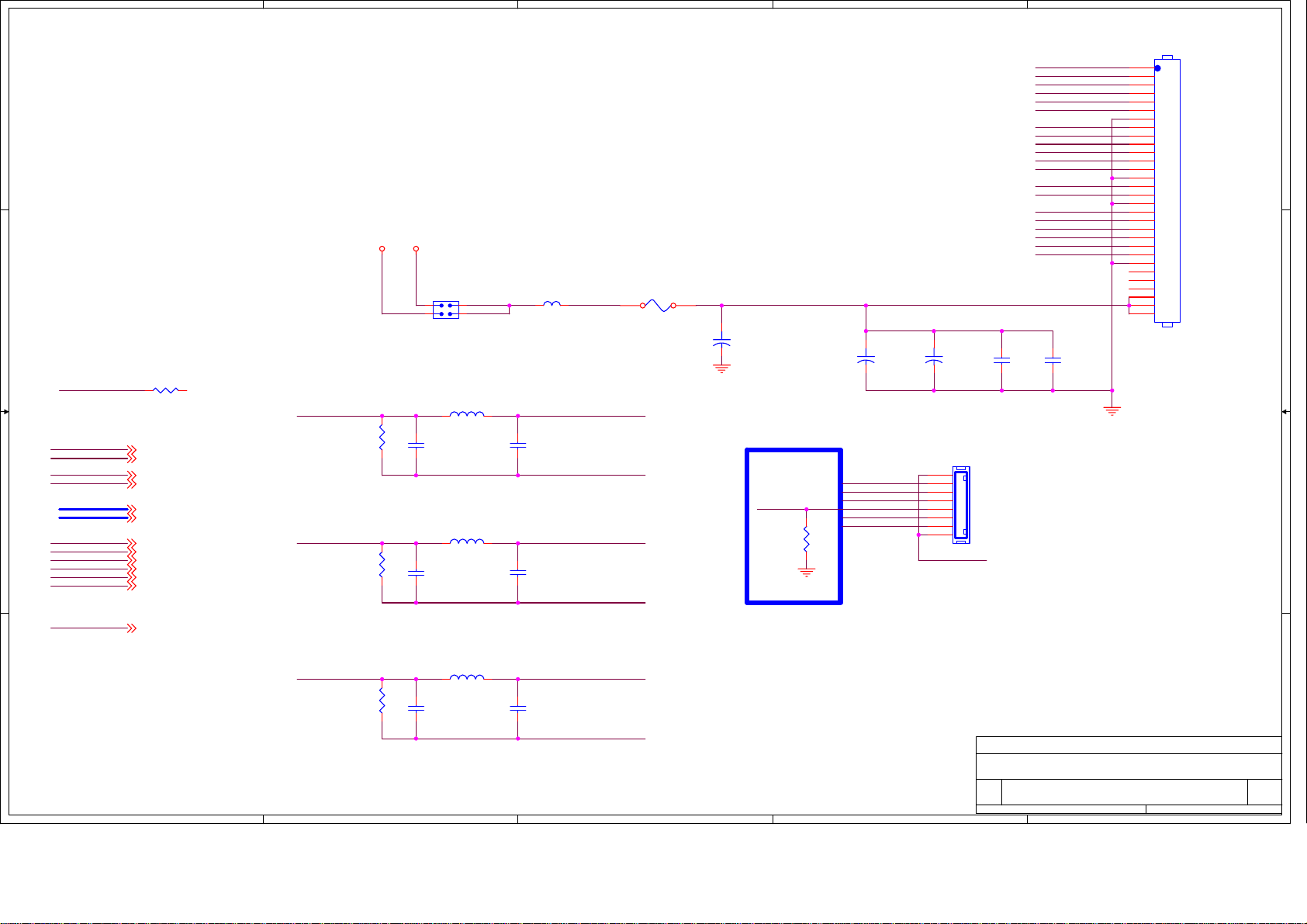
A
B
C
D
E
LVDS OUT
4 4
3 3
GPIO
2 2
CLK1+
CLK1-
CLK2+
CLK2-
AP[0..7]
AN[0..7]
R
G
B
SVM
VSYNC
HSYNC
GPIO
R277
2k
CLK1+ 3
CLK1- 3
CLK2+ 3
CLK2- 3
AP[0..7] 3
AN[0..7] 3
R3
G3
B3
SVM 3
VSYNC 3
HSYNC 3
GPIO 3
R
R278
75 1%
G
R279
75 1%
VCC+12V
1 2
3 4
JP2
2x2
JP2X2/DIP/P2.54
L75
0.082uH
L/IND/SMD/0603
C149
33pF
L76
0.082uH
L/IND/SMD/0603
C151
33pF
L3
FB
BEAD/SMD/0805
C150
33pF
C152
33pF
LVDS
RED_OUT
GND
GRN_OUT
GND
F1
4A/?v
FUSE/DIP/P10.0
CE86
+
330uF/25v
C330UF25V/D8H14
SVM
R366
75
CE87
+
220uF/16v
CRT OUT
RED_OUT
GRN_OUT
BLU_OUT
HSYNC
VSYNC
CE88
+
220uF/16v
J9
1
2
3
4
5
6
7
8
GND
8x1 W/HOUSING
DIP8/W/H/P2.54
CB185
0.1uF
LVDSVDDLVDSVDD
AN0
AP0
AN1
AP1
AN2
AP2
CLK1CLK1+
AN3
AP3
AN4
AP4
AN5
AP5
AN6
AP6
CLK2CLK2+
AN7
AP7
CB186
0.1uF
J8
1
2
3
4
5
6
7
8
9
10
11
12
13
14
15
16
17
18
19
20
21
22
23
24
25
26
27
28
29
30
FI-SE30P-HF
LVDS/30P/P1.25/S
1 1
R281
75 1%
A
B
L78
0.082uH
L/IND/SMD/0603
C154
33pF
C155
33pF
GND
BLU_OUTB
Title
LCD TV - MediaTek MT8205 Solution
Size Doc Number Rev
B
C
D
Date: Sheet of
LVDS/CRT OUT
14 16Tuesday, May 10, 2005
E
V0.1
Page 25
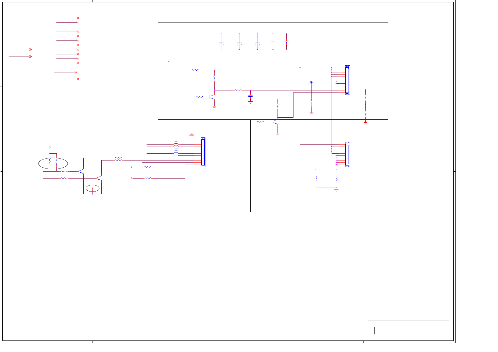
A
B
C
D
E
UP1_2
4.7K
UP1_2 6
UP3_1 6,8
OBO0 3
OBO1 3
OBO2 3
OBO3 3
OBO4 3
OBO5 3
OBO6 3
OBO7 3
UP3_0 6
PWM0 3
KEYPAD - MAX 8-KEYS
3 2
Q1
1
2N3906
DV33A
Q2
1
2N3906
R2 510
R4 510
3 2
DV33A
5VSB
VCC
OBO0
L81 FB
OBO1 MENU
L82 FB
OBO2
OBO3
OBO4
OBO5
L83 FB
L84 FB
L85 FB
L86 FB
POWER ON/OFF
LED_RED
LED_GRN
UP1_2
R81 0
R57 0
IR & POWER ON LED
R336 0
R288
PWM0
4.7k
1
TV/AV
2
3
VOL-
4
VOL+
5
CH-
6
CH+
7
IR
8
9
10
11
12
Inverter_PWR
R285
10k
Q12
1
Back Light circuit
2N3904
SOT23/SMD
J12
12x1 W/HOUSING
DIP12/W/H/P2.0
+
CE1
470uF/50v
UP3_1
4 4
URST#
IR
3 3
URST# 3,6
IR 3
R0603/SMD
OBO0
OBO1
OBO2
OBO3
OBO4
OBO5
OBO6
OBO7
UP3_0
PWM0
5VSB
R14
R13
10K
10K
R0603/SMD
R9 4.7K
OBO6
R10
OBO7
PANEL INVERTER POWER
CE2
+
470uF/50v
3 2
R286
100k
UP3_0
CB190
0.1uF
+
R293
4.7k
CE3
470uF/50v
1
CB1
0.1uF
Inverter_PWR
Dimming
VCC
R291
10k
BL_ON/OFF
Q13
2N3904
SOT23/SMD
CB2
0.1uF
Inverter_PWR
FOR CHI-MEI INVERTER
CONNECTOR
PWR_GND
J10
1
2
3
4
5
TP1
R50
0
3 2
Inverter_PWR
PWR_GND
L89
FB
BEAD/SMD/1206
6
7
8
9
10
11
12
12x1 W/HOUSING R.A
DIP12/WH/P2.0/R
SELECT
J11
1
2
3
4
5
6
7
8
9
10
10x1 W/HOUSING R.A.
DIP10/WH/P2.0/R
L90
FB
BEAD/SMD/1206
R. ANGLE
VCC
SELECT Hi For External
SELECT Low For Inte rna l
R289
R
R290
0
R. ANGLE
2 2
1 1
Title
LCD TV - MediaTek MT8205 Solution
Size Doc Number Rev
C
Date: Sheet of
A
B
C
D
BACK_LIGHT/KEYPAD
E
15 16Tuesday, May 10, 2005
V0.1
Page 26

TUNER1 IN
D
TUNER1
TUNER
FQ1236 / : NTSC TV
TU1
FQ1236-MK3
GND1
GND2
VS_TUNER3SCL4AS6SDA52nd SIF OUT11AF-R9AF-L10CVBS12GND3
NC1NC2NC7NC
8
TH1
TH2
GNDS
GNDS
VCC
TU_SCL
TU_SDA
SIF1_IN TU_CVBS
AF1_IN
ADDRESS
C2 86
AF /MPX14VS_IF
13
TH3
GNDS
54321
6
Date
P#
IF
AV , TUNER I/O
TU_VCC
1J1
TU_12V
GND4
TH4
1R1
1 2
18
12
12
1R3
56
FB2
0
1R2 0
1 2
1R4 0
1 2
TVTU_CVBS
TV_GND
12
FB1
0
GNDS
GNDS
SIF1_OUT
AF1_OUT
TV_GND
TV
1
2
3
4
5
SDA
6
SCL
7
8
9
10
11
12
CON12
M1
9
2
9
8
3
8
7
4
7
6
5
6
NC
GND HOLE
1
M2
9
2
8
3
7
4
6
5
2
2
9
3
3
8
4
4
7
5
5
6
NC
GND HOLE
1
GNDSGNDS
D
C
12
1C6 10nF
1 2
1L4
1.5uH/1.2uH
SIF_12V
12
12
1R8
1R7
1k
1.8K
1
12
12
3 2
1R10
220
12
1C1 10nF
1 2
GND V
SIF1
TU_VCC
12
CE6
+
10uF/25v
GNDS
TU_12V SIF_12V
TU_12V
12
+
12
CE8
100uF/16V
1L5 FB
1 2
12
CE3
CB3
+
100uF/16V
0.1uF
100uF/16V
1L6 FB
1 2
12
CB6
0.1uF
GNDS
GNDSGNDV
GND V
GNDS
VIDEO GROUNDAUDIO GROUND
VCC
12
12
CE4
+
12
12
CE5
CB4
+
100uF/16V
CB5
0.1uF
0.1uF
GNDS
SIF_12V
12
12
CE9
CB7
+
220uF/16V
0.1uF
GND V
1Q1
2N3904
1R11
10
1R12
1C9
71.5
NC
1 2
GND VGND VGND V
1R5 100
1 2
TU_SCL
1R6
1 2
TU_SDA
1C2
1C3
47pF
47pF
1 2
1 2
SCL
100
SDA
TUNER1 SIF1 BPF
NTSC 4.5MHz PAL 6MHz
1C4 10nF
1 2
SIF1_IN
1R9 0
1 2
1C5 22pF/27pF
1 2
12
1L3
1C7
1.5uH/1.2uH
820pF/560pF
1 2
GND VGND V
1L2 47uH/22uH
1 2
1C8
820pF/560pF
1 2
GND V GND V
B
CE7
+
1 2
AF1_IN
AF1
33uF/16V
1R14 0
1 2
AF1
1R15 0
1 2
SIF1 SIF1_OUT
1R16 0/NC
SIF1_IN SIF1_OUT
AF1_OUT
1 2
AF1_OUT
SIF1_OUT
TU_12V
TU_12V
TU_VCC
TU_VCC
A
C
B
A
1 2 3 4 5 6
Page 27

54321
C1
12
22pF NPO
12
5%
1 2
R7
5%
10K
R17
5%
100K
1 2
R21
10K
R1
82K
1 2
12
C5
NPO
4.7nF
C8
4.7uF
X5R
U1
1
PIN
2
NIN
3
AGND
EN4BS
ATA-120
12
C15
2.2UF
C21
12
22pF NPO
12
5%
R14
82K
12
C27
NPO
4.7nF
C30
12
4.7uF
X5R
1
PIN
2
NIN
3
AGND
4
EN
C34
NS
A
R2
5%
100K
PGND
SW
VPP
R16
1 2
100K
U3
PGND
ATA-120
+24V
12
12
+
C4
C7
C6
100NF
1 2
X7R
8
7
6
C9
5
1 2
1UF
X5R
D2
6.2V
100UF/25V
1UF
X7R
L5 10uH
1 2
12
12
R8
R9
10
5%
12
C17
390PF
NPO
10K
5%
D1
MBRS130LTR
12
+24V
5%
C28
100NF
1 2
X7R
8
7
SW
6
VPP
BS
C32
5
1 2
1UF
X5R
D4
6.2V
12
12
+
C25
C29
100UF/25V
1UF
X7R
L6 10uH
1 2
12
12
5%
12
C36
390PF
NPO
R23
R22
10
10K
5%
D3
MBRS130LTR
D
+24V
12
12
R11
10K
R10
10K
5%
C14
22UF/16V
AUSPL
C20
10UF
5%
R66
R47
12
4K7
1K8
5%
5%
C541nC55
R4
100K
1 2
C
B
AUSPR
C40
10UF
R45
R33
12
4K7
1K8
5%
5%
R19
C521nC53
100K
5%
1 2
5%
R67
1 2
12
12
4K7
5%
1n
C19
22UF/16V
R46
12
12
4K7
5%
1n
3
R12
2
10K 5%
12
R37
10K
5%
R39
1 2
10K 5%
U2A
+
-
AGND
C24
22pF
R15 47K
1 2
12
R36
10K
5%
U2B
5
+
6
-
OUT
AGND
1 2
12
+
C10
C12
100UF/25V
100NF
C3
1
RC4558
5%
1 2
+24V
R3
12
5%
1UF
10K
X5R
MUTEC
R5
5%
100K
1 2
1 2
R18
C31
5%
1 2
7
OUT
RC4558
C41
22pF
47K
R38
5%
1UF
X5R
12
10K
MUTEC
5%
6
D
FILM
C38
1 2
+
1000UF/25V
12
R6
10
C11
470NF
5%
C16
C
100NF
1 2
X7R
B
C39
1 2
+
1000UF/25V
12
C33
470NF
FILM
12
R20
10
5%
C35
100NF
1 2
X7R
A
A
Title
Number Revis ionSize
B
Date: 2-Sep-2005 Sheet of
File: D:\
1 2 3 4 56
正在进行的项目\LCD TV\LC D TV.Dd bDrawn By:
Page 28

54321
R24
3K
12
5%
D
+24V
D6
1N4148
AGND
D8
1N4148
R43
C
0R
D5
NC
R30
22k
D9
R54 10K
1 2
C22
5%
5%
22U/16V
R51 10K
1 2
R52 22K
1 2
R62 10K
1 2
R59 10K
1 2
R64 22K
1 2
B
AUSPL
R48 1k8
C60
1 2
12
10UF
X5R
R49 4K7
1 2
12
5%
5%
R53
1n
100K
R50 4K7
1 2
12
5%
C45
C46
1n
1 2
R56 1k8
C59
1 2
A
AUSPR
12
10UF
X5R
R57 4K7
1 2
12
5%
5%
R60
1n
100K
R58 4K7
1 2
12
5%
C47
C48
1n
1 2
5%
5%
1 2
5%
5%
C44
22U/16V
5%
1 2
5%
R55 10K
1 2
U5A
3
+
2
-
RC4558
C49
22P
R63 10K
1 2
U5B
5
+
6
-
RC4558
C50
22P
AGND
AGND
12
100U/35V
1
+24V
C2
C13
100N
C26
10U/16V
R13
12
5%
1K
R65
47K
5%
1 2
5%
OUT
AGND
1N4148
MUTE
LOUT
ROUT
+24V
5%
C43
R26
7
OUT
10U/16V
12
5%
1K
R61
47K
5%
1 2
AGND
1 2 3 4 56
Q1
2N3906
12
+
C42
100UF/25V
4.7V
AGND
J10
R42
1k
D7
Q4
2N3906
12
+
C18
NC
R28
1k
12
+
C51
220UF/25V
AGND
Q7
NC
R27
NC
AGND
R40
10K
12
12
5%
R41
5%
10K
AGND AGND
D10
NC
R34
12
5%
1K
MUTEB
R35
1 2
5%
1K
AGND
AGND
rca2
Title
B
Date: 2-Sep-2005 Sheet of
File: D:\
12
R25
5%
10K
1 2
Q2
2N3904
LOUT
Q5
2N3904
ROUT
Q6
2N3904
Number Revis ionSize
正在进行的项目\LCD TV\LC D TV.Dd bDrawn By:
6
MUTEC
C37
1UF
X5R
Q3
2N3904
R29
1K
5%
D
12
MUTE
AGND
C
B
A
Page 29

54321
6
F1
L
D
250VAC 5A
R2
1.6M
R1
CX1
1.6M
0.33U
N
C
LCD-TV 200W S M P S SP E C:
1. +5V 4A
2. +5VS 1A (Standby 5V)
3. +12V 2A
4.+24V 4A
5. +24VA 1A
B
A
+5V
+5V
+5V
GND
GND
GND
+12V
+12V
+5VS
+5VS
GND
GND
ON/OFF
+24V
+24V
+24V
GND
GND
GND
+24VA
+24VA
GND
GND
1 2 3 4 5 6
D1
STTH3L06
L3
1 2
400UH
C52
22NF
3 4
C6
R6
68K
25V 1U
C5
680NF
2
5
$0.28
8
VCC
ZCD
COMP
U1
L6562
3
MULT
C4
10NF
GND
6
R27
5.6K
R26
6.8K
C21
0.1UF
V_BUKE
C37
R47
1000V 10nF
30K
R48
30K
C53
35V 47U
6
5
4
3
ZD3
C55
C54
22V
35V 47U
0.1U
L2
L1
10mH
10mH
1
CX2
0.33
1
J1
1
2
3
4
5
6
7
8
PH-2.0
J2
1
2
3
4
5
PH2.0
J3
1
2
3
4
5
6
PH2.5
J4
1
2
3
4
PH2.0
2
CY1
250V1000P
4
STBR608
BD1
3
CY2
250V1000P
R4
1.6M
C1
R5
2
1.6M
1UF 630V
C2
Q2
BC337
Q3
BC327
35V 22U
Q5
BC327
43
50V 22UF
R65
10K
100NF
R25
20R
C3
C20
R66
10K
U4A
PC817
R3
20K
R24
10K
D3
PQ32-20
STTH8R06
R8
36K
1
D2
Q1
1N4148
INV
7
GD
10R
R7
CS
4
15
DCL
11
PGND
12
SGND
14
DIS
C22
50V 2.2U
SHORT CIRCUIT PROTECTION
C38
10NF
R49
R67
U5
Vstr
Drain
NC
Vfb
GND
Vcc
FSDM0565
STBY
16
R28
15K
47K/1W
10R
10R
$0.60
STP20NM50
R10
R9
0.33R
0.33R
R30
22R
3
9
DC
VC
L5991
M1
RCT
VREF
2
4
R29
5.6K
C23
3.3NF
D11
R51
120K
R50
C39
10nF
D10
FER107
FER104
D9
FER104
D14
1
2
U6
PC817B
NTC1
C24
8.2N
V_BUKE
V_BUKE
2.5R
R15
R13
1.8M
750K
R14
8
750K
VCC
R11
8.2K
R12
1.6K
1N4148
50V 4.7U
1
2
3
4
5
6
VFB5COMP
R52
C40
TR3
??
1
SYNC
4.7K
$0.45
ISEN
6SS7
C25
3.3N
R31
1K
EC28
R16
1.8M
R17
100K
R18
C7
10N
10
OUT
13
43
R53
130K
14
13
12
10
9
8
卧式
R68
1K
U7
TL431
20K
PC817
U3A
R54
R69
1.2K
C8
C9
450V 100UF
D6
10R
43K
R32
C26
220PF
R55
10R 2W
D12 ??
16V 2200U
470R/1W
R70
68K
R19
450V 100UF
D4
STTH310
1N4148
R33
1K
Q6
BC327
C41
R80
1.2K
C56
47nF
R34
1KV 472P
C42
1KV 4700P
Q4
0.47R 3W
C10
25V 2200U
R71
R72
5.6K
TR1
PQ3220
PQ3220
R36
OPEN
STP12NK80
OPEN
R35
L7
C43
C44
16V 2200U
Q9
STP22NF0
5.6K
1
2
5
6
??
1
2
5
6
TR2
??
C27
0.47R 3W
CY3
250V 2200P
10UH
R73
R74
Q10
BC337
12
+24V4A
10
11
+12V
8
9
+24V1A
7
12
+24V4A
10
11
+12V
8
9
+24V1A
7
R56
R57
C57
16V 470U
47K
4.7K
GND
0.01R
+5VS
1A
0.01R
C45
25V 470U
+5V
4A
+12V
Q11
BC337
C11
1KV 470P
R21
100R 2W
D5
R20
??
100R 2W
C12
1KV 470P
C13
1KV 470P
D7
??
C28
1KV 470P
D8
??
L8
L
AGND
R59
2.0K
12
R58
56K
Q7
BC337
4.7K
R75
R37
100R 2W
C29
1KV 470P
C46
1KV 470P
U4B
PC817
C58
100N
C15
C16
C14
35V 1000U
35V 1000U
R22
100R 2W
C31
C33
C30
C32
25V 470U
25V 1000U
25V 1000U
R39
1K
R38
100R 2W
R60
100R 2W
C48
C47
25V 1000U
25V 1000U
+12V
+24V
R76
R77
4.7K
10K
Title
Date: 3-Jun-2005 Sheet of
File:
10UH
L4
C17
R23
470R/1W
35V 470U
35V 470U
L5
470R/1W
25V 470U
R40
1.2K
12
U3B
R41
22K
U2
TL431
C49
R62
470R/1W
25V 470U
AGND
R61
4.7K
BZX79C12RL
ZD2
27V
ZD1
R78
4.7K
Q12
BC337
C59
100N
ON
STBY
ON/OFF
LCD-TV 200W SMPS Sch
Number RevisionSize
Orcad C
+24V
4A
C19
C18
0.1U
D
35V 470U
10UH
C35
R42
+12V
2A
C36
0.1U
25V 470U
R46
R44
33.2K
30K
C34
0.1UF
R43
R45
2.7K
75K
10UH
L6
+24VA
C51
C50
0.1U
C
1A
25V 470U
B
R64
4.7K
1N4148
Q8
D13
MMBT3906
Q13
R79
4.7K
MMBT3904
A
Ver1.0
1/1
R63
1K
Page 30

Basic Operations & Circuit Description
Main Electric Components
(1). MODULE:
There are 1 pc. panel and 2 pcs. PCB including 1 pc. INVERTER
board(L), 1 pc. T-CONTROL board,
(2).SIGNAL PROCESS
There are 4 pcs. PCBs including
1 pc. Audio&Tuner board,
1 pc. Main digital board,
1 pc. Keypad board,
1 pc. Remote Control Receiver board,
(3).POWER
There are 1 pc. PCB for power.
Page 31

PCB function
1. Power:
(1). Input voltage: AC 100V~240V, 47Hz~63Hz.
Input range: AC 90V(Min)~264V(Max) auto regulation.
(2). To provide power for PCBs.
a). +24V for Inverter.
b). +5Vsb for standby,
c). +5V for signal power,
d). +24V for Audio Amp power and converter to
e). +12V for Tuner power.
2. Main (Video InterFace) board:
(1).Decoder the video signal (TV,CVBS,S-VIDEO) from analog to digital
signal.
(2).Converter the Video signals( TV,CVBS,S-VIDEO ) and graphics signal
(VGA,YPbPr) from internace to progressive,
(3). Converter the Digital to fit the panel display mode and output the LVDS
signal to Panel.
3. Tuner & Audio Board:
(1)
(2 ). Decoder the TV SIF signal to audio signal,
(3 ). Converter the audio to audio Ampifile and out put to the speaker.
4. KEYBOARD
To get the main button control on LCD_TV as SOURCE,MENU,
CHANEL +,CHANEL -, VOL +,VOL-, STANDBY functions.
5. Remote control board
Receive the remote signal and active for the control.
6. T-CONTROL board
7. INVERTER board
Convert TV RF signal to video and audio signal to Main board.
Converter the LVDS signal to the digital signal for fitting the PANEL.
Converter the low DC voltage +24V to high AC voltage to drive the backlight.
Page 32

PCB failure analysis
1. CONTROL:
a. Abnormal noise on screen.
b. No picture.
2. MAIN (VIDEO):
a. Lacking color, Bad color scale.
b. No voice.
c. No picture but with signals output, OSD and back light.
d. Abnormal noise on screen.
3. POWER:
No picture, no power output.
Basic operation of LCD-TV
1. After turning on power switch, power board sends 5Vst-by Volt to Micro
Processor IC waiting for ON signals from Key Switch or Remote Receiver.
2. When the ON signal from Key Switch or Remote Receiver is detected, Micro
Processor will send ON Control signals to Power. Then Power sends (5Vsc,
12Vsc, 24V and RLY ON, Vs ON) to PCBs working. This time VIF will send
signals to display back light, OSD on the panel and start to search available
signal sources. If the audio signals input, them will be amplified by Audio AMP
and transmitted to Speakers.
3. If some abnormal signals are detected (for example: over volts, over current,
over temperature and under volts), the system will be shut down by Power off.
Page 33

LCD basic display theory.
When an electrical field is applied to the LC planes, the LC molecules re-align
themselves so that they are parallel to the electrical field. This electrical process
is known as twisted nematic field effect or TNFE. In this alignment, polarized
light is not twisted as it passes through the LC material (see Diagram 3A and
3B). If the front polarizer is oriented perpendicular to the rear polarizer, light will
pass through the energized display but will be blocked by the rear polarizer. An
LCD in this form is acting as a light shutter.
Displays with variable characters are created by selectively etching away the
conductive surface that was originally deposited on the glass. Etched areas
become the display’s background; unetched areas become the display’s
characters.
Diagram 3A. The “off” state of a TN LCD-the LC molecules form a twist and therefore
cause polarized light to twist as it passes through.
Diagram 3B. The “on” state-the electrical field re-aligns the LC molecules so they do
not twist the polarized light.
Page 34

Disassembly
In case of trouble, etc., Necessitating disassemble, please disassemble in the order shown in the
illustrations.
Reassemble in the reverse order.
1. Removal of the Back Cover
2. Removal of the MAIN PCB
a. Remove the screws.
.
b
Slide out the LCD chassis slightly; pull up the connector of AC cord from PCB; pull up the
PCB from LCD.
LCD
c
. Remove the Anode cap from The picture tube. To avaid a shock hazard, be sure to discharge
.
d
Take out the LCD chassis.
Page 35

IC DESCRIPTION
-MT8205G
-AT24C02
-MX29LV160BBTC
-LP2996
-AZ1117 /H
-WM8776
-MX232A
-ISAV330
Page 36

Pinout information
AC18
C3
D3
C1
C2
L11
D1
D2
F2
D4
E1
E2
E3
E4
F1
F4
F3
G3
J3
G4
H3
K3
K4
J4
H4
L3
G2
G1
H2
H1
M12
J2
J1
K2
K1
L4
L2
L1
M2
M1
M11
N2
N1
P2
P1
M3
R2
R1
T2
T1
N12
N3
M4
N4
N11
T4
P3
R3
P4
U4
R4
U3
V4
T3
U1
U2
V1
V2
V3
W1
W2
AC9
W3
W4
Y1
Y2
Y3
P11
Y4
AA1
AA2
AA3
AA4
AB1
AB2
AB3
AB4
AC1
AC2
AC3
AC4
R11
AD1
AD2
AD3
AD4
AE1
VFEVDD1
ADCVDD4
SIF
AF
ADCVSS4
REFP4
REFN4
ADCVSS
ADIN4
ADIN3
ADIN2
ADIN1
ADIN0
ADCVDD
PWM2VREF
AUXVTOP
AUXVBOTTO M
VPLLVSS
VPLLVDD
DLLVDD
DLLVSS
BGVSS
REXTA
BGVDD
LVDDA
A7P
A7N
CLK2P
U?
CLK2N
LVSSA
A6P
A6N
A5P
A5N
LVDDB
A4P
A4N
A3P
A3N
LVSSB
CLK1P
CLK1N
A2P
A2N
LVDDC
A1P
A1N
A0P
A0N
LVSSC
DACVDDC
VREF
FS
DACVSSC
SVM
DACVDDB
DACVSSB
DACVDDA
G
DACVSSA
B
R
DE
VSYNC O
HSYNCO
VCLK
EBO7
EBO6
EBO5
EBO4
DVDD3I
EBO3
EBO2
EBO1
EBO0
EGO7
DVSS18
EGO6
EGO5
EGO4
EGO3
EGO2
EGO1
EGO0
ERO7
ERO6
ERO5
DVDD18
ERO4
ERO3
ERO2
DVSS3
ERO1
ERO0
OBO7
OBO6
OBO5
D5
C4
L12
AVCM
VFEVSS1
ADCVDD0
OBO3
OBO4
OBO2
AF1
AE2
AF2
C5
A4
L13
A2
A3
A1
B5
B1
CVBS2P
CVBS2N
OBO0
OBO1
AF3
AE3
A5
B2
B3
B4
SCN
REFP0
REFN0
CVBS1P
CVBS0P
CVBS1N
CVBS0N
ADCVSS0
ADCVDD1
OGO6
OGO2
OGO1
OGO4
OGO5
OGO7
OGO3
DVDD3
DVSS18
T11
AF4
AF5
AC6
AD5
AC5
AE4
AD6
AE5
AD9
SCP
OGO0
D7
D6
C6
N13
A6
M13
B7
B6
SYP
SYN
VOCM
REFP1
REFN1
VFEVDD0
ADCVSS1
C8
A10
C7
D9
B10
B8
A7
VICM
VFEVSS0
ADCVDD2
C9
D10
A9
A8
B9
YP
YN
SOY
CBP
CRP
CBN
CRN
REFP2
REFN2
ADCVSS2
A13
D8
A11
A12
B13
B11
B12
C13
C12
C14
N14
L14
C10
C11
D11
RP
GP
RN
GN
MON1
MON0
ADCVDD3
D14
D13
D12
BP
BN
SOG
DVSS
DVDD
REFP3
VSYNC
REFN3
HSYNC
ADCVSS3
ADCPLLVSS1
MT8205
AD5
AD6
ORO7
ORO4
ORO0
ORO6
ORO1
ORO3
ORO2
ORO5
DVDD18
AE6
AF8
AD7
AD8
AF6
AC8
AE7
AF7
AC7
AD18
AD0
HIGHA2
HIGHA6
HIGHA0
HIGHA3
HIGHA1
HIGHA5
HIGHA4
HIGHA7
DVSS18
P12
AE9
AF9
AE15
AF12
AF10
AE10
AC11
AD11
AD7
AD1
AD4
DVSS3
AD2
AD3
DVDD18
R12
AF17
AE16
AF16
AC19
AD16
AC16
AD15
AC15
A16
DVDD3I
IOA3
IOA7
IOA1
IOA4
IOA0
IOA6
IOA2
IOA5
AE8
AF14
AF13
AE14
AE13
AC10
AC13
AD14
AD17
AD13
A15
A16
B14
B15
B16
B17
A14
C15
L15
C16
D15
M14
D16
TESTP
TESTN
XTALVDD
SYSPLLVSS
ADCPLLVSS
SYSPLLVDD
ADCPLLVDD
ADCPLLVDD 1
A17
IOA19
IOA21
IOA18
IOA20
IOOE#
IOALE
DVSS18
T12
AF11
AE12
AE11
AF15
AE17
AC17
AD12
A17
D18
C18
D17
M15
C17
VI0
VI2
VI1
XTALI
XTALO
APLLVSS
APLLVDD
XTALVSS
APLL_CAP
DMPLLVSS
DMPLLVDD
IOCS#
DVDD3
DVDD18
UP15
WR#
INT0#
RD#
UP14
UP12
UP13
IOWR#
AF18
AF19
AE18
AE20
AE19
AF20
AD19
AC12
AD20
AC14
AD10
A20
E23
A18
B19
B18
A19
C20
C19
D19
D20
L16
VI9
VI3
VI5
VI8
VI4
VI6
VI7
VI11
VI10
DVDD18
FCICLK
UP17
UP34
UP30
UP31
DVSS18
UP35
PRST#
FCICMD
UP16
P13
AF22
AF21
AC20
AF23
AE21
AE22
AD22
AD21
AC22
AC21
A22
A21
B20
C21
D21
VI13
VI12
VI14
DVSS3
GPIO0
PWM1
PWM0
FCIDAT
AE23
AF24
AC23
AD23
A23
B21
B22
M16
VI15
IR
AE24
B23
C22
C23
D22
D23
VI17
VI19
VI21
VI23
VI16
VI18
VI20
VI22
DVSS18
DVSS3
ICE
SCL
RXD
TXD
R13
AF25
AE25
AD24
AC24
SCL0
SDA
AF26
VSYNC_DVI
HSYNC_DVI
SDA0
SCL1
AE26
AB23
VCLK_DVI
DE_DVI
DVDD18
AOSDATA0
AOSDATA1
AOSDATA2
DVDD3I
AOSDATA3
AOBCK
AOLRCK
AOMCLK
DVSS3
DQ24
DQ25
DQ26
DVDD2
DQ27
DQ28
DVSS2
DQ29
DVDD2
DQ30
DQ31
DQS3
DQM1
DVSS18
DQS2
DQ23
DQ22
DVSS2
DQ21
DQ20
DVDD18
DQ19
DVDD2
DQ18
DQ17
DQ16
DVSS2
DVSS18
RA11
DVDD2
RCLK
RCLKB
DVSS2
RA10
DVDD2I
DVDD18
RCS#
RAS#
DVSS2
CAS#
RWE#
DQ10
DVDD2
DQ11
DVSS18
DQ12
DQ13
DVSS2
DQ14
DQ15
DQS1
AVSS18
AVDD18
RVREF
DVSS18
DQM0
DQS0
DVDD2
DVSS2
DVDD2
SDA1
AB24
LIN
RA4
RA5
RA6
RA7
RA8
RA9
CKE
RA3
RA2
RA1
RA0
BA1
BA0
DQ8
DQ9
DQ7
DQ6
DQ5
DQ4
DQ3
DQ2
DQ1
DQ0
C24
D24
A24
Y24
A25
A26
B26
F23
B25
B24
C26
C25
E24
N15
G26
G25
F26
F24
F25
E26
N16
E25
G24
D26
D25
H25
H26
P14
J25
J26
K25
P16
K26
L25
AA24
L26
H24
M25
M26
N25
J23
R16
J24
K23
K24
L23
R14
L24
M23
N26
H23
P26
P25
P15
M24
N23
N24
R26
P24
P23
U23
AA23
R24
R23
T24
R15
T23
U24
W26
V25
V26
V23
U25
T13
U26
T25
T15
T26
R25
W25
W23
Y23
G23
T16
Y26
Y25
AA26
V24
AA25
AB26
T14
AB25
AC26
W24
AC25
AD26
AD25
BGA388/SOCKET
MT8205
12
Page 37

Pin Descriptions
2.3 Pin Descriptions
Table 2-1 provides detail video/audio port pin descriptions.
Table 2-1 video/audio port pin descriptions.
Pin Symbol Type Description
E24
C25
C26
A25
A26
B26
B25
B24
A3
A2
A1
C1
C2
AOMCLK
AOLRCK
AOBCK
AOSDATA0
AOSDATA1
AOSDATA2
AOSDATA3
LIN
CVBS0P
CVBS1P
CVBS2P
SIF
AF
O Audio out master clock
O Audio out left-right clock
O Audio out bit clock
O Audio out data line 0
O Audio out data line 1
O Audio out data line 2
O Audio out data line 3
I Audio line in
I Composite Video input 0
I Composite Video input 1
I Composite Video input 2
I Tuner Sound SIF
I Tuner Sound AF
13
Page 38

AT24C01A/2/4/8/16
2-Wire
Serial CMOS
E2PROM
1K (128 x 8)
2K (256 x 8)
4K (512 x 8)
8K (1024 x 8)
16K (2048 x 8)
0180C
AT24C01A/02/04/08/16
Features
Low Voltage and Standard Voltage Operation
•
5.0 (V
2.7 (V
2.5 (V
1.8 (V
Internally Organized 128 x 8 (1K), 256 x 8 (2K), 512 x 8 (4K),
•
1024 x 8 (8K) or 2048 x 8 (16K)
2-Wire Serial Interface
•
Bidirectional Data Tra ns fer Protocol
•
100 kHz (1.8V, 2.5V, 2.7 V) and 400 kHz (5V) Com patibility
•
Write Protect Pin for Hardware Data Pro tec tio n
•
8-Byte Page (1K, 2K), 16-Byte Page (4K, 8K, 16K) Write Modes
•
Partial Page Writes Are Allowe d
•
Self-Timed Write Cycle (1 0 ms max )
•
High Reliabili ty
•
Endurance: 1 Mill io n Cycles
Data Retention: 100 Years
Automotive Grade and Extended Temperature Dev ices Available
•
8-Pin and 14-Pin JEDEC SOIC and 8-Pin PDI P Packages
•
Description
The AT24C01A/02/04/08/16 provides 1024/2048/4096/8192/16384 bits of serial electrically er asable and programmable read only memor y (EEPROM) organized as
128/256/512/1024/2048 words of 8 bits each. The device is optimized for use in many
industrial and commercial applications where low power and low voltage oper ation are
essential. The AT24C01A/02/04/08/16 is available in space saving 8-pin PDIP, 8-pin
and 14-pin SOIC packages and is accessed via a 2-wire serial interface. In addition,
the entire family is available in 5.0V (4.5V to 5.5V), 2.7V (2.7V to 5.5V), 2.5V (2.5V to
5.5V) and 1.8V (1.8V to 5.5V) versions.
= 4.5V to 5.5V)
CC
= 2.7V to 5.5V)
CC
= 2.5V to 5.5V)
CC
= 1.8V to 5.5V)
CC
Pin Configurations
Pin Name Function
A
to A
0
2
SDA Serial Data
SCL Serial Clock Input
WP Write Protect
NC No Connect
14-Pin SOIC
8-Pin PDIP
Address Inputs
8-Pin SOIC
2-25
Page 39

Absolute Maximum Rat ings*
Operating Temperature...................-55°C to +125°C
Storage Temperature...................... -65°C to +150°C
Voltage on Any Pin
with Respect to Ground ..................... -0.1V to +7.0V
Maximum Operating Voltage ...........................6.25V
DC Output Current.........................................5.0 mA
Block Diagram
*NOTICE: Stresses beyond those listed unde r “Absolu te Maxi-
mum Ratings” may cause permanent da ma ge to th e de vice .
This is a stress rating only and functional operation of the
device at these or any other conditions beyond those indicated in the operational sections of this specification is not
implied. Exposure to absolute maximum rating conditions
for extended periods may affect device reliability.
Pin Description
SERIAL CLOCK (SCL): The SCL input is used to positive
edge clock data into each E
edge clock data out of each device.
SERIAL DATA (SDA): The SDA pin is bidirectional for serial data transfer. This pin is open-drain driv en and may be
wire-ORed with any number of other open-drain or open
collector devices.
DEVICE/PAGE ADDRESSES (A2, A1, A0): The A2, A1
and A0 pins are device address inputs that ar e har d wir ed
for the AT24C01A and the AT24C02. As many as eight
1K/2K devices may be addressed on a single bus system
(device addressing is discussed in detail under the Device
Addressing section).
2-26 AT24C01A/02/04/08/16
2
PROM device and negative
The AT24C04 uses the A2 and A1 inputs for hard wire
addressing and a total of four 4K devices may be addressed on a single bus system. The A0 pin is a no connect.
The AT24C08 only uses the A2 input for hardwire addressing and a total of two 8K devices may be addressed
on a single bus system. The A0 and A1 pins are no connects.
The AT24C16 does not use the device address pins which
limits the number of devices on a single bus to one. The
A0, A1 and A2 pins are no connects.
(continued)
Page 40

FEATURES
R
MX29LV160BT/BB
16M-BIT [2Mx8/1Mx16] CMOS SINGLE VOLTAGE
3V ONLY FLASH MEMORY
• Extended single - supply voltage range 2.7V to 3.6V
• 2,097,152 x 8/1,048,576 x 16 switchable
• Single power supply operation
- 3.0V only operation for read, erase and program
operation
• Fully compatible with MX29LV160A device
• Fast access time: 70/90ns
• Low power consumption
- 30mA maximum active current
- 0.2uA typical standby current
• Command register architecture
- Byte/word Programming (9us/11us typical)
- Sector Erase (Sector structure 16K-Bytex1,
8K-Bytex2, 32K-Bytex1, and 64K-Byte x31)
• Auto Erase (chip & sector) and Auto Program
- Automatically erase any combination of sectors with
Erase Suspend capability.
- Automatically program and verify data at specified
address
• Erase Suspend/Erase Resume
- Suspends sector erase operation to read data from,
or program data to, any sector that is not being erased,
then resumes the erase.
• Status Reply
- Data polling & Toggle bit for detection of program and
erase operation completion.
• Ready/Busy pin (RY/BY)
- Provides a hardware method of detecting program or
erase operation completion.
• Sector protection
- Hardware method to disable any combination of
sectors from program or erase operations
- Temporary sector unprotect allows code changes in
previously locked sectors.
• CFI (Common Flash Interface) compliant
- Flash device parameters stored on the device and
provide the host system to access
• 100,000 minimum erase/program cycles
• Latch-up protected to 100mA from -1V to VCC+1V
• Boot Sector Architecture
- T = Top Boot Sector
- B = Bottom Boot Sector
• Low VCC write inhibit is equal to or less than 1.4V
• Package type:
- 44-pin SOP
- 48-pin TSOP
- 48-ball CSP
• Compatibility with JEDEC standard
- Pinout and software compatible with single-power
supply Flash
• 10 years data retention
GENERAL DESCRIPTION
The MX29L V160BT/BB is a 16-mega bit Flash memo ry
organized as 2M bytes of 8 bits or 1M words of 16 bits.
MXIC's Flash memories offer the most cost-effective
and reliable read/write non-volatile random access
memory. The MX29LV160BT/BB is packaged in 44-pin
SOP, 48-pin TSOP and 48-ball CSP. It is designed to be
reprogrammed and erased in system or in standard
EPROM programmers.
The standard MX29LV160BT/BB o ff ers access time as
fast as 70ns, allowing operation of high-speed microprocessors without wait states. To eliminate bus contention, the MX29LV160BT/BB has separate chip enable
(CE) and output enable (OE) controls.
MXIC's Flash memories augment EPROM functionality
with in-circuit electrical erasure and progr amming. The
MX29LV160BT/BB uses a command register to manage this functionality. The command register allows f or
P/N:PM1041 REV. 1.2, JUL. 01, 2004
100% TTL level control inputs and fixed power supply
levels during erase and programming, while maintaining
maximum EPROM compatibility.
MXIC Flash technology reliably stores memory contents
ev en after 100,000 erase and program cycles . The MXIC
cell is designed to optimize the erase and programming
mechanisms. In addition, the combination of advanced
tunnel oxide processing and low internal electric fields
for erase and program operations produces reliable cycling. The MX29LV160BT/BB uses a 2.7V~3.6V VCC
supply to perform the High Reliability Erase and auto
Program/Erase algorithms.
The highest degree of latch-up protection is achieved
with MXIC's proprietary non-epi process. Latch-up protection is proved for stresses up to 100 milliamps on
address and data pin from -1V to VCC + 1V.
1
Page 41

LP2996
DDR Termination Regulator
LP2996 DDR Termination Regulator
November 2003
General Description
The LP2996 linear regulator is designed to meet the JEDEC
SSTL-2 specifications for termination of DDR-SDRAM. The
device contains a high-speed operational amplifier to provide
excellent response to load transients. The output stage prevents shoot through while delivering 1.5A continuous current
and transient peaks up to 3A in the application as required
for DDR-SDRAM termination. The LP2996 also incorporates
aV
output as a reference for the chipset and DIMMs.
An additional feature found on the LP2996 is an active low
shutdown (SD) pin that provides Suspend To RAM (STR)
functionality. When SD is pulled low the VTToutput will
tri-state providing a high impedance output, but, V
remain active. A power savings advantage can be obtained
in this mode through lower quiescent current.
pin to provide superior load regulation and a V
SENSE
REF
REF
will
Typical Application Circuit
Features
n Source and sink current
n Low output voltage offset
n No external resistors required
n Linear topology
n Suspend to Ram (STR) functionality
n Low external component count
n Thermal Shutdown
n Available in SO-8, PSOP-8 or LLP-16 packages
Applications
n DDR-I and DDR-II Termination Voltage
n SSTL-2 and SSTL-3 Termination
n HSTL Termination
20057518
© 2003 National Semiconductor Corporation DS200575 www.national.com
Page 42

TSSOP − PW
TE330
SCDS164A – MAY 2004 − REVISED MAY 2004
D Low Differential Gain and Phase
(D
= 0.64%, DP = 0.1 Degrees Typ)
G
D Wide Bandwidth (BW = 300 MHz Min)
D Low Crosstalk (X
= −63 dB Typ)
TALK
D Low Power Consumption
(I
= 3 µA Max)
CC
D Bidirectional Data Flow, With Near-Zero
Propagation Delay
D Low ON-State Resistance (r
D V
D I
Operating Range From 4.5 V to 5.5 V
CC
Supports Partial-Power-Down Mode
off
= 3 Ω Typ)
on
Operation
D Data and Control Inputs Provide
Undershoot Clamp Diode
D Control Inputs Can Be Driven by TTL or
5-V/3.3-V CMOS Outputs
D Latch-Up Performance Exceeds 100 mA Per
JESD 78, Class II
D ESD Performance Tested Per JESD 22
− 2000-V Human-Body Model
(A114-B, Class II)
− 1000-V Charged-Device Model (C101)
D Suitable for Both RGB and
Composite-Video Switching
D, DBQ, OR PW PACKAGE
(TOP VIEW)
16
1
IN
15
2
S1
A
S2
A
D
A
S1
B
S2
B
D
B
GND
RGY PACKAGE
14
3
13
4
12
5
11
6
10
7
9
8
(TOP VIEW)
IN
116
S1
2
A
S2
3
A
D
4
A
S1
5
B
S2
6
B
D
7
B
89
GND
V
D
V
EN
S1
S2
D
S1
S2
D
CC
C
CC
D
C
15
14
13
12
11
10
D
D
C
C
EN
S2
D
S2
D
D
D
S1
C
S2
C
description/ordering information
The TI TS5V330 video switch is a 4-bit 1-of-2 multiplexer/demultiplexer with a single switch-enable (EN) input.
When EN
is disabled and the high-impedance state exists between the D and S ports. The select (IN) input controls the
data path of the multiplexer/demultiplexer.
is low, the switch is enabled and the D port is connected to the S port. When EN is high, the switch
ORDERING INFORMATION
T
A
QFN − RGY Tape and reel TS5V330RGYR TE330
SOIC − D
−40°C to 85°C
†
Package drawings, standard packing quantities, thermal data, symbolization, and PCB design guidelines
are available at www.ti.com/sc/package.
Please be aware that an important notice concerning availability, standard warranty, and use in critical applications of
Texas Instruments semiconductor products and disclaimers thereto appears at the end of this data sheet.
SSOP (QSOP) − DBQ T ape and reel TS5V330DBQR TE330
PACKAGE
†
Tube TS5V330D
Tape and reel TS5V330DR
Tube TS5V330PW
Tape and reel TS5V330PWR
ORDERABLE
PART NUMBER
TOP-SIDE
MARKING
TS5V330
!"# $"%&! '#(
'"! ! $#!! $# )# # #* "#
'' +,( '"! $!#- '# #!#&, !&"'#
#- && $##(
POST OFFICE BOX 655303 • DALLAS, TEXAS 75265
Copyright 2004, Texas Instruments Incorporated
1
Page 43

Page 44

19-0175; Rev 3; 5/96
±15kV ESD-Protected, +5V RS-232 Transceivers
_______________General Description
The MAX202E–MAX213E, MAX232E/MAX241E line
drivers/receivers are designed for RS-232 and V.28
communications in harsh environments. Each
transmitter output and receiver input is protected
against ±15kV electrostatic discharge (ESD) shocks,
without latchup. The various combinations of features
are outlined in the
receivers for all ten devices meet all EIA/TIA-232E and
CCITT V.28 specifications at data rates up to 120kbps,
when loaded in accordance with the EIA/TIA-232E
specification.
The MAX211E/MAX213E/MAX241E are available in 28pin SO packages, as well as a 28-pin SSOP that uses
60% less board space. The MAX202E/MAX232E come
Selection Guide.
The drivers and
____________________________Features
♦ ESD Protection for RS-232 I/O Pins:
±15kV—Human Body Model
±8kV—IEC1000-4-2, Contact Discharge
±15kV—IEC1000-4-2, Air-Gap Discharge
♦ Latchup Free (unlike bipolar equivalents)
♦ Guaranteed 120kbps Data Rate—LapLink™
Compatible
♦ Guaranteed 3V/µs Min Slew Rate
♦ Operate from a Single +5V Power Supply
_________________Pin Configurations
in 16-pin narrow SO, wide SO, and DIP packages. The
MAX203E comes in a 20-pin DIP/SO package, and
needs no external charge-pump capacitors. The
MAX205E comes in a 24-pin wide DIP package, and
also eliminates external charge-pump capacitors. The
MAX206E/MAX207E/MAX208E come in 24-pin SO,
SSOP, and narrow DIP packages. The MAX232E/
MAX241E operate with four 1µF capacitors, while the
MAX202E/MAX206E/MAX207E/MAX208E/MAX211E/
MAX213E operate with four 0.1µF capacitors, further
reducing cost and board space.
________________________Applications
Notebook, Subnotebook, and Palmtop Computers
Battery-Powered Equipment
Hand-Held Equipment
Ordering Information appears at end of data sheet.
TOP VIEW
C1+
1
V+
2
C1-
3
C2+
C2-
T2OUT
R2IN
Pin Configurations and Typical Operating Circuits continued at
end of data sheet.
MAX202E
4
MAX232E
5
V-
6
7
8
DIP/SO
V
CC
16
GND
15
T1OUT
14
R1IN
13
R1OUT
12
T1IN
11
T2IN
10
R2OUT
9
_____________________________________________________________Selection Guide
MAX202E–MAX213E, MAX232E/MAX241E
PART
MAX202E
MAX203E
MAX205E
MAX206E
MAX207E
MAX208E
MAX211E
MAX213E
MAX232E
MAX241E
LapLink is a registered trademark of Traveling Software, Inc.
No. of RS-232
DRIVERS
2 2 0 4 (0.1µF) No No
2 2 0 None No No
5 5 0 None Yes Yes
4 3 0 4 (0.1µF) Yes Yes
5 3 0 4 (0.1µF) No No
4 4 0 4 (0.1µF) No No
4 5 0 4 (0.1µF) Yes Yes
4 5 2 4 (0.1µF) Yes Yes
2 2 0 4 (1µF) No No
4 5 0 4 (1µF) Yes
________________________________________________________________
No. of RS-232
RECEIVERS
RECEIVERS
ACTIVE IN
SHUTDOWN
No. of
EXTERNAL
CAPACITORS
LOW-POWER
SHUTDOWN
Maxim Integrated Products
TTL THREE-
STATE
Yes
1
For free samples & the latest literature: http://www.maxim-ic.com, or phone 1-800-998-8800
Page 45

±15kV ESD-Protected, +5V RS-232 Transceivers
Table 3. DB9 Cable Connections
Commonly Used for EIA/TIAE-232E and
V.24 Asynchronous Interfaces
PIN CONNECTION
Received Line Signal
Detector (sometimes
1
called Carrier Detect,
DCD)
2 Receive Data (RD) Data from DCE
3 Transmit Data (TD) Data from DTE
4 Data Terminal Ready Handshake from DTE
5 Signal Ground
6 Data Set Ready (DSR) Handshake from DCE
7 Request to Send (RTS) Handshake from DTE
8 Clear to Send (CTS) Handshake from DCE
9 Ring Indicator Handshake from DCE
____________Pin Configurations and Typical Operating Circuits (continued)
Handshake from DCE
Reference point for
signals
TOP VIEW
C1+
1
V+
2
C1-
MAX202E–MAX213E, MAX232E/MAX241E
C2+
T2OUT
R2IN
3
MAX202E
4
C2-
MAX232E
5
V-
6
7
8
V
CC
16
GND
15
T1OUT
14
R1IN
13
R1OUT
12
T1IN
11
T2IN
10
R2OUT
9
DIP/SO
PIN NUMBERS ON TYPICAL OPERATING CIRCUIT REFER TO DIP/SO PACKAGE, NOT LCC.
* 1.0µF CAPACITORS, MAX232E ONLY.
+5V INPUT
0.1µF*
0.1µF*
TTL/CMOS
INPUTS
TTL/CMOS
OUTPUTS
6.3V
16V
0.1µF
1
3
4
5
11
10
12
9
C1+
+5V TO +10V
VOLTAGE DOUBLER
C1C2+
+10V TO -10V
C2-
VOLTAGE INVERTER
T1IN
T2IN
R1OUT
R2OUT
T2
V
T1
GND
0.1µF*
16
CC
R1
5k
R2
5k
15
14 ______________________________________________________________________________________
6.3V
T1OUT
T2OUT
R1IN
R2IN
2
V+
V-
+10V
-10V
6
0.1µF*
16V
14
RS-232
OUTPUTS
7
13
RS-232
INPUTS
8
Page 46

TFT LCD Preliminary Specification
MODEL NO.: V270B1 - L01
LCD TV Head Division
AVP
QRA Dept.
DDIII DDII DDI
Approval Approval Approval Approval
陳永一 李汪洋 藍文錦 林文聰
LCD TV Marketing and Product Management Division
Product Manager
郭振隆
TVHD / PDD
陳立宜 謝芳宜
1
Page 47

- CONTENTS -
REVISION HISTORY
1. GENERAL DESCRIPTION
1.1 OVERVIEW
1.2 FEATURES
1.3 APPLICATION
1.4 GENERAL SPECIFICATIONS
1.5 MECHANICAL SPECIFICATIONS
2. ABSOLUTE MAXIMUM RATINGS
2.1 ABSOLUTE RATINGS OF ENVIRONMENT
2.2 ELECTRICAL ABSOLUTE RATINGS
2.2.1 TFT LCD MODULE
2.2.2 BACKLIGHT UNIT
3. ELECTRICAL CHARACTERISTICS ------------------------------------------------------- 7
3.1 TFT LCD MODULE
3.2 BACKLIGHT INVERTER UNIT
3.2.1 CCFL(Cold Cathode Fluorescent Lamp) CHARACTERISTICS
3.2.2 INVERTER CHARACTERISTICS
3.2.3 INVERTER INTERTFACE CHARACTERISTICS
4. BLOCK DIAGRAM
4.1 TFT LCD MODULE
5. INTERFACE PIN CONNECTION
5.1 TFT LCD MODULE
5.2 BACKLIGHT UNIT
5.3 INVERTER UNIT
5.4 BLOCK DIAGRAM OF INTERFACE
5.5 LVDS INTERFACE
5.6 COLOR DATA INPUT ASSIGNMENT
6. INTERFACE TIMING
6.1 INPUT SIGNAL TIMING SPECIFICATIONS
6.2 POWER ON/OFF SEQUENCE
7. OPTICAL CHARACTERISTICS
7.1 TEST CONDITIONS
7.2 OPTICAL SPECIFICATIONS
8. DEFINITION OF LABELS ------------------------------------------------------- 26
8.1 CMO MODULE LABEL
9. PACKAGING
9.1 PACKING SPECIFICATIONS
9.2 PACKING METHOD
10. PRECAUTIONS
10.1 ASSEMBLY AND HANDLING PRECAUTIONS
10.2 SAFETY PRECAUTIONS
11. MECHANICAL CHARACTERISTICS ------------------------------------------------------- 30
------------------------------------------------------- 3
------------------------------------------------------- 4
------------------------------------------------------- 5
------------------------------------------------------- 12
------------------------------------------------------- 13
------------------------------------------------------- 19
------------------------------------------------------- 22
------------------------------------------------------- 27
------------------------------------------------------- 29
2
Page 48

REVISION HISTORY
Version Date
Ver 1.0 Jun. 15,’05 All All Preliminary Specification was first issued.
Page
Section Description
(New)
3
Page 49

1. GENERAL DESCRIPTION
1.1 OVERVIEW
V270B1- L01 is a TFT Liquid Crystal Display module with 14-CCFL Backlight unit and 1ch-LVDS
interface. The display diagonal is 27”. This module supports 1366 x 768 WXGA format and can display true
16.7M colors(8-bits colors). The inverter module for backlight is built-in.
1.2 FEATURES
- Excellent brightness (550 nits)
- Ultra high contrast ratio (1000:1)
- Fast response time (8ms)
- High color saturation NTSC 75%
- WXGA (1366 x 768 pixels) resolution
- DE (Data Enable) only mode
- LVDS (Low Voltage Differential Signaling) interface
- Optimized response time for both 50/60 Hz frame rate
- Ultra wide viewing angle: 176(H)/176(V) (CR>20) Super MVA technology
- 180 degree rotation display option
- Low color shift function option
- Color reproduction (Nature color)
1.3 APPLICA TION
- TFT LCD TVs
- High brightness, multi-media displays
-
1.4 GENERAL SPECIFICATI0NS
Item Specification Unit Note
Active Area 596.259 (H) x 335.232 (V) (27” diagonal) mm
Bezel Opening Area 603.22 (H) x 341.98 (V) mm
Driver Element a-si TFT active matrix -
Pixel Number 1366 x R.G.B. x 768 pixel
Pixel Pitch (Sub Pixel) 0.1460 (H) x 0.4365 (V) mm
Pixel Arrangement RGB vertical stripe -
Display Colors 16.7M color
Display Operation Mode Transmissive mode / Normally black -
Surface Treatment
Hardness : 3H, Haze : 40%
Anti-reflective coating < 2% reflection
-
1.5 MECHANICAL SPECIFICATIONS
Item Min. Typ. Max. Unit Note
Horizontal(H) 636.85 637.55 638.25 mm
Module Size
Note (1) Please refer to the attached drawings for more information of front and back outline dimensions.
Vertical(V) 379.1 379.8 380.5 mm
Depth(D) 33.9 35.4 36.9 mm To PCB cover
Depth(D) 39.2 40.7 42.2 mm To inverter cover
Weight 3700 4000 4300 g
(1)
4
Page 50

2. ABSOLUTE MAXIMUM RATINGS
2.1 ABSOLUTE RATINGS OF ENVIRONMENT
Item Symbol
Storage Temperature TST -20 +60 ºC (1)
Operating Ambient Temperature TOP 0 +50 ºC (1), (2)
Shock (Non-Operating) S
Vibration (Non-Operating) V
Note (1) Temperature and relative humidity range is shown in the figure below.
(a) 90 %RH Max. (Ta ≦ 40 ºC).
(b) Wet-bulb temperature should be 39 ºC Max. (Ta > 40 ºC).
(c) No condensation.
Note (2) The maximum operating temperature is based on the test condition that the surface temperature of
display area is less than or equal to 60 ºC with LCD module alone in a temperature controlled chamber.
Thermal management should be considered in final product design to prevent the surface temperature of
display area from being over 60 ºC. The range of operating temperature may degrade in case of improper
thermal management in final product design.
Note (3) 11 ms, half sine wave, 1 time for ± X, ± Y, ± Z.
- 50 G (3), (5)
NOP
- 1.0 G (4), (5)
NOP
Min. Max.
Value
Unit Note
Note (4) 10 ~ 500 Hz, 10 min, 1 time each X, Y, Z.
Note (5) At testing Vibration and Shock, the fixture in holding the module has to be hard and rigid enough
so that the module would not be twisted or bent by the fixture.
Relative Humidity (%RH)
100
90
80
60
Operating Range
40
20
10
Storage Range
-40 -20 0 20 40 60 80
Temperature (ºC)
5
Page 51

2.2 ELECTRICAL ABSOLUTE RATINGS
2.2.1 TFT LCD MODULE
Te st
-
Value
Unit Note
(1)
Min. Type Max. Unit Note
0
-0.3
-
-
3000 V
30 V
7 V
RMS
(1), (3)
Item Symbol
Min. Max.
Power Supply Voltage Vcc -0.3 6.0 V
Input Signal Voltage VIN -0.3 3.6 V
2.2.2 BACKLIGHT UNIT
Item Symbol
Lamp Voltage VW
Power Supply Voltage VBL
Control Signal Level
Note (1) Permanent damage to the device may occur if maximum values are exceeded. Functional
operation should be restricted to the conditions described under normal operating conditions.
Note (2) No moisture condensation or freezing.
Note (3) The control signals includes Backlight On/Off Control, Internal PWM Control, External PWM
Condition
Ta = 25 ℃ - -
- -
(1)
Control and Internal/External PWM Selection.
6
Page 52

3. ELECTRICAL CHARACTERISTICS
3.1 TFT LCD MODULE Ta = 25 ± 2 ºC
Parameter Symbol
Min. Typ. Max.
Power Supply Voltage VCC 4.5 5.0 5.5 V (1)
Power Supply Ripple Voltage VRP - - 150 mV
Rush Current I
- - 3.0 A (2)
RUSH
White - 1.8 - A
Power Supply Current
Differential Input High
LVDS
Interface
Threshold Voltage
Differential Input Low
Threshold Voltage
Common Input Voltage V
Terminating Resistor R
Black - 1.2 - A
Vertical Stripe
ICC
- 1.65 - A
V
- - +100 mV
LVT H
V
-100 - - mV
LVT L
1.125 1.25 1.375 V
LVC
100 ohm
T
Input High Threshold Voltage VIH 2.7 - 3.3 V CMOS
interface
Input Low Threshold Voltage VIL 0 - 0.7 V
Note (1) The module should be always operated within above ranges.
Note (2) Measurement Conditions:
+5.0V
Q1 2SK1475
R1
47K
Value
FUSE
C3
1uF
Unit Note
Vcc
(LCD Module Input)
(3)
(High to Low)
(Control Signal)
SW
+12V
C1
1uF
VR1
R2
1K
47K
0.01uF
Q2
2SK1470
C2
Vcc rising time is 470us
+5V
0.9Vcc
0.1Vcc
GND
470us
7
Page 53

Note (3) The specified power supply current is under the conditions at Vcc = 5 V, Ta = 25 ± 2 ºC, fv = 60 Hz,
whereas a power dissipation check pattern below is displayed.
a. White Pattern
Active Area
c. Vertical Stripe Pattern
b. Black Pattern
Active Area
R
G
G
B
R
B
B
R
R
G
G
B
B
R
Active Area
3.2 BACKLIGHT INVERTER UNIT
3.2.1 CCFL (Cold Cathode Fluorescent Lamp) CHARACTERISTICS (
Parameter Symbol
Lamp Voltage VW
Lamp Current IL
Lamp Starting Voltage VS
Operating Frequency FO 50 - 70 KHz (3)
Lamp Life Time LBL
Min. Typ. Max.
- 1120 -
4.2 4.7 5.2
- -
- -
50,000 60,000
Value
B
R
1650
1500
- Hrs (4)
R
B
G
R R
Ta = 25 ± 2 ºC)
Unit Note
V
RMS
mA
RMS
V
RMS
V
RMS
B
G
R
B
G
B
G
I
(1)
(2), Ta = 0 ºC
(2), Ta = 25 ºC
= 4.7mA
L
8
Page 54

A
A
A
A
A
A
A
A
A A A
A
A
A
3.2.2 INVERTER CHARACTERISTICS (
Parameter Symbol
Ta = 25 ± 2 ºC)
Value
Min. Typ. Max.
Power Consumption PBL - 92 - W (5), IL = 4.7mA
Power Supply Voltage VBL
Power Supply Current IBL
22.8 24 25.2
-
3.8
-
Input Ripple Noise - - - 500 mV
Backlight Turn on
Voltage
1790 - -
V
BS
1200 - - V
V
Oscillating Frequency FW 53 56 59 kHz
Dimming Frequency FB 150 160 170 Hz
Minimum Duty Ratio D
- 10 - %
MIN
Note (1) Lamp current is measured by utilizing high frequency current meters as shown below:
LCD
Module
HV (Pink)
HV (White)
HV (Pink)
HV (White)
HV (Pink)
HV (White)
HV (Pink)
HV (White)
HV (Pink)
HV (White)
HV (Pink)
HV (White)
HV (Pink)
HV (White)
1
2
1
2
1
2
Inverter
1
2
1
2
1
2
1
2
LV (Gray)
Unit Note
VDC
A Non Dimming
VBL =22.8V
P-P
Ta = 0 ºC
RMS
Ta = 25 ºC
RMS
Note (2) The lamp starting voltage V
should be applied to the lamp for more than 1 second under starting
S
up duration. Otherwise the lamp could not be lighted on completed.
Note (3) The lamp frequency may produce interference with horizontal synchronous frequency from the
display, and this may cause line flow on the display. In order to avoid interference, the lamp
frequency should be detached from the horizontal synchronous frequency and its harmonics as far
as possible.
9
Page 55

Note (4) The life time of a lamp is defined as when the brightness is larger than 50% of its original value
and the effective discharge length is longer than 80% of its original length (Effective discharge
length is defined as an area that has equal to or more than 70% brightness compared to the
brightness at the center point.) as the time in which it continues to operate under the condition Ta
= 25 ±2℃ and I
= 4.2 ~ 5.2 mA
L
RMS
.
Note (5) The power supply capacity should be higher than the total inverter power consumption P
the pulse width modulation (PWM) mode was applied for backlight dimming, the driving current
changed as PWM duty on and off. The transient response of power supply should be considered
for the changing loading when inverter dimming.
3.2.3 INVERTER INTERTFACE CHARACTERISTICS
Item Symbol
On/Off Control
Voltage
Internal/External
PWM Select Voltage
Internal PWM
Control Voltage
External PWM
Control Voltage
ON
V
BLON
OFF
HI
V
SEL
LO
MAX
V
V
IPWM
MIN
HI 2.0
V
V
EPWM
LO
Te st
Condition
-
-
-
-
= L
SEL
= H
SEL
Min. Typ. Max. Unit Note
2.0
-
5.0 V
0
2.0
-
-
0.8 V
5.0 V
0
- -
-
0
-
0
-
-
0.8 V
3.0 V minimum duty ratio
-
V maximum duty ratio
5.0 V duty on
0.8 V duty off
. Since
BL
Control Signal Rising Time T
Control Signal Falling Time T
PWM Signal Rising Time T
PWM Signal Falling Time T
Input impedance R
BLON Delay Time T
BLON Off Time T
- - - 100 ms
r
- - - 100 ms
f
- - - 50 us
PWMR
- - - 50 us
PWMF
- 1 - - MΩ
IN
- 1 - - ms
on
- 1 - - ms
off
Note (1) The SEL signal should be valid before backlight turns on by BLON signal. It is inhibited to change
the internal/external PWM selection (SEL) during backlight turn on period.
10
Page 56

Note (2) The power sequence and control signal timing are shown as the following figure.
BL
V
V
V
V
BLON
V
SEL
EPWM
IPWM
V
0
Ton
Toff
2.0V
0
0.8V
Backlight on duration
Tr Tf
2.0V
0
0.8V
Ext. Dimming Function
T
T
PWMR
PWMF
Int. Dimming Function
2.0V
0
0.8V
3.0V
0
W
External
PWM
Period
External
PWM Duty
Minimun
100%
Duty
11
Page 57

4. BLOCK DIAGRAM
4.1 TFT LCD MODULE
RX0(+/-)
RX1(+/-)
RX2(+/-)
RX3(+/-)
RXCLK(+/-)
Vcc
GND
VBL
GND
VBL
GND
SEL
E_PWM
I_PWM
BLON
CN1
CN2
INPUT CONNECTOR
(JAE,FI-X 0SSL-HF) 3
INVERTER CONNECTOR
CN1:S10B-PH-SM3-TB(D)(LF)(JST)
CN2: S12B-PH-SM3-TB(D)(LF)(JST)
FRAME BUFFER
TIMING
CONTROLLER
DC/DC CONVERTER &
REFERENCE VOLTAGE
CN10: S2B-ZR-SM3A-TF (D)(LF)(JST)
SCAN DRIVER IC
TFT LCD PANEL
(1366x3x768)
DA TA DRIVER IC
CN3-CN9:SM02 (8.0)B-BHS-1-TB(LF)(JST)
BACKLIGHT
UNIT
12
Page 58

y
(3)
t
(5)
(4)
(6)
5. INTERFACE PIN CONNECTION
5.1 TFT LCD MODULE
CNF1 Connector Pin Assignment
Pin No. S
1 GND Ground
2 RPF Display Rotation
3 SELLVDS Select LVDS data forma
4 NC No Connection
5 NC No Connection
6 ODSEL Overdrive Lookup Table Selection
7 EN LCS Low Color Shift
8 GND Ground
9 RX0- Negative transmission data of pixel 0
10 RX0+ Positive transmission data of pixel 0
11 RX1- Negative transmission data of pixel 1
12 RX1+ Positive transmission data of pixel 1
13 RX2- Negative transmission data of pixel 2
14 RX2+ Positive transmission data of pixel 2
15 RXCLK- Negative of clock
16 RXCLK+ Positive of clock
17 RX3- Negative transmission data of pixel 3
18 RX3+ Positive transmission data of pixel 3
19 GND Ground
20 GND Ground
21 GND Ground
22 GND Ground
23 GND Ground
24 GND Ground
25 GND Ground
26 VCC Power supply: +5V
27 VCC Power supply: +5V
28 VCC Power supply: +5V
29 VCC Power supply: +5V
30 VCC Power supply: +5V
Note (1) Connector Part No.: FI-X30SSL-HF(JAE) or compatible
mbol Description Note
(2)
Note (2) Reserved for internal use. Left it open.
Note (3) Low : normal display (default), High : display with 180 degree rotation
Note (4) Overdrive lookup table selection. The Overdrive lookup table should be selected in accordance to the
frame rate to optimize image quality.
ODSEL Note
L Lookup table was optimized for 60 Hz frame rate.
H Lookup table was optimized for 50 Hz frame rate.
Note (5) Please refer to 5.5 LVDS INTERFACE (Page 17)
Note (6) Enable Low color shift function.
EN LCS Note
L Low color shift off
H Low color shift on
13
Page 59

5.2 BACKLIGHT UNIT
The pin configuration for the housing and leader wire is shown in the table below.
CN3-CN9 (Housing): BHR-03VS-1 (JST)
Pin No. Symbol Description
1 HV High Voltage Pink
2 HV High Voltage White
Note (1) The backlight interface housing for high voltage side is a model BHR-03VS-1, manufactured by JST.
The mating header on inverter part number is SM02(8.0)B-BHS-1-TB(LF) or equivalent.
Wire Color
CN10 (Housing): ZHR-2 (JST) or equivalent
Pin No. Symbol Description
1 LV Low Voltage (+) Gray
2 NC No Connection -
Note (2) The backlight interface housing and return cable for low voltage side is a model ZHR-2 , manufactured
by JST or equivalent. The mating header on inverter part number is S2B-ZR-SM3A-TF(D)(LF) or
equivalent.
Wire Color
14
Page 60

5.3 INVERTER UNIT
CN1(Header):S10B-PH-SM3-TB(D)(LF)(JST) or equivalent.
Pin Name Description
1
2
3
4
5
6
7
8
9
10
CN2(Header): S12B-PH-SM3-TB(D)(LF)(JST) or equivalent.
Pin Name Description
1
2
3
4
5
6
7
8
9
VBL +24V Power input
GND Ground
VBL +24V Power input
GND Ground
Internal/external PWM selection
SEL
High : external dimming
Low : internal dimming
External PWM control signal
10
11
12
CN3-CN9(Header): SM02(8.0)B-BHS-1-TB(LF)(JST) or equivalent
Pin Name Description
1
2
CN10(Header): S2B-ZR-SM3A-TF(D)(LF)(JST) or equivalent
Pin Name Description
1
2
E_PWM
I_PWM
BLON Backlight on/off control
CCFL HOT
CCFL HOT
CCFL COLD
NC
E_PWM should be connected to low when internal
PWM was selected (SEL = low).
Internal PWM control signal
I_PWM should be connected to ground when
external PWM was selected (SEL = high).
CCFL high voltage
CCFL high voltage
CCFL low voltage
-
Note (1) Floating of any control signal is not allowed.
15
Page 61

0
0
G0-G
0
G0-G
5.4 BLOCK DIAGRAM OF INTERFACE
CNF1
Rx0+
-
R0-R7
TxIN
7
B
-B7
DE
Rx
Rx1+
Rx1-
Rx2+
Rx2-
Rx3+
-
Host
Graphics
Controller
PLL
CLK+
-
LVDS Transmitter
THC63LVDM83A
(LVDF83A)
51Ω
100pF
51Ω
51Ω
100pF
51Ω
51Ω
100pF
51Ω
51Ω
100pF
51Ω
51Ω
100pF
51Ω
LVDS Receiver
THC63LVDF84A
PLL
RxOUT
R0-R7
7
B
-B7
DE
DCLK
Timing
Controller
R0~R7 : Pixel R Data ,
G0~G7 : Pixel G Data ,
B0~B7 : Pixel B Data ,
DE : Data enable signal
Note (1) The system must have the transmitter to drive the module.
Note (2) LVDS cable impedance shall be 50 ohms per signal line or about 100 ohms per twist-pair line when it is
used differentially.
16
Page 62

5.5 LVDS INTERFACE
SIGNAL
TRANSMITTER
THC63LVDM83A
INTERFACE
CONNECTOR
RECEIVER
THC63LVDF84A
TFT CONTROL
INPUT
SELLVDS
=L
R0
R1
R2
R3
R4
R5
G0
G1
G2
G3
G4
G5
B0
B1
24
bit
B2
B3
B4
B5
DE
R6
R7
G6
G7
B6
B7
RSVD 1
RSVD 2
RSVD 3
R0~R7: Pixel R Data (7; MSB, 0; LSB)
SELLVDS
=H
R2
R3
R4
R5
R6
R7
G2
G3
G4
G5
G6
G7
B2
B3
B4
B5
B6
B7
DE
R0
R1
G0
G1
B0
B1
RSVD 1
RSVD 2
RSVD 3
DCLK 31 TxCLK IN TxCLK OUT+
PIN INPUT Host TFT-LCD PIN OUTPUT
51
52
54
55
56
3
4
6
7
11
12
14
15
19
20
22
23
24
30
50
2
8
10
16
18
25
27
28
TxIN0
TxIN1
TxIN2
TxIN3
TxIN4
TxIN6
TxIN7
TxIN8
TxIN9
TxIN12
TxIN13
TxIN14
TxIN15
TxIN18
TxIN19
TxIN20
TxIN21
TxIN22
TxIN26
TxIN27
TxIN5
TxIN10
TxIN11
TxIN16
TxIN17
TxIN23
TxIN24
TxIN25
TA OUT0+
TA OUT0-
TA OUT1+
TA OUT1-
TA OUT2+
TA OUT2-
TA OUT3+
TA OUT3-
TxCLK OUT-
Rx 0+
Rx 0-
Rx 1+
Rx 1-
Rx 2+
Rx 2-
Rx 3+
Rx 3-
RxCLK IN+
RxCLK IN-
SELLVDS
=L
Rx OUT0
27
Rx OUT1
29
Rx OUT2
30
Rx OUT3
32
Rx OUT4
33
Rx OUT6
35
Rx OUT7
37
Rx OUT8
38
Rx OUT9
39
Rx OUT12
43
Rx OUT13
45
Rx OUT14
46
Rx OUT15
47
Rx OUT18
51
Rx OUT19
53
Rx OUT20
54
Rx OUT21
55
Rx OUT22
1
Rx OUT26
6
Rx OUT27
7
Rx OUT5
34
Rx OUT10
41
Rx OUT11
42
Rx OUT16
49
Rx OUT17
50
Rx OUT23
2
Rx OUT24
3
Rx OUT25
5
26 RxCLK OUT DCLK
R0
R1
R2
R3
R4
R5
G0
G1
G2
G3
G4
G5
B0
B1
B2
B3
B4
B5
DE
R6
R7
G6
G7
B6
B7
NC
NC
NC
SELLVDS
=H
R2
R3
R4
R5
R6
R7
G2
G3
G4
G5
G6
G7
B2
B3
B4
B5
B6
B7
DE
R0
R1
G0
G1
B0
B1
NC
NC
NC
G0~G7: Pixel G Data (7; MSB, 0; LSB)
B0~B7: Pixel B Data (7; MSB, 0; LSB)
DE : Data enable signal
Notes(1) RSVD(reserved)pins on the transmitter shall be “H” or “L”.
17
Page 63

5.6 COLOR DATA INPUT ASSIGNMENT
The brightness of each primary color (red, green and blue) is based on the 8-bit gray scale data input for
the color. The higher the binary input, the brighter the color. The table below provides the assignment of
color versus data input.
Data Signal
Color
R7 R6 R5 R4 R3 R2 R1 R0 G7 G6 G5 G4 G3 G2 G1 G0 B7 B6 B5 B4 B3 B2 B1 B0
0
0
1
1
0
0
0
0
0
0
1
1
1
1
1
1
0
0
0
0
0
0
:
:
:
:
1
1
1
1
1
1
0
0
0
0
0
0
:
:
:
:
0
0
0
0
0
0
0
0
0
0
0
0
:
:
:
:
0
0
0
0
0
0
Basic
Colors
Gray
Scale
Of
Red
Gray
Scale
Of
Green
Gray
Scale
Of
Blue
Black
Red
Green
Blue
Cyan
Magenta
Yellow
White
Red(0) / Dark
Red(1)
Red(2)
:
:
Red(253)
Red(254)
Red(255)
Green(0) / Dark
Green(1)
Green(2)
:
:
Green(253)
Green(254)
Green(255)
Blue(0) / Dark
Blue(1)
Blue(2)
:
:
Blue(253)
Blue(254)
Blue(255)
Note (1) 0: Low Level Voltage, 1: High Level Voltage
Red Green Blue
0
0
0
0
0
0
0
0
0
0
0
0
0
0
0
0
0
0
0
0
0
0
0
0
0
0
0
0
0
0
0
0
1
1
1
1
1
1
0
0
0
0
0
1
1
1
1
1
1
1
1
0
0
0
0
0
0
1
1
1
1
1
0
0
0
0
0
0
0
0
0
0
0
0
0
0
1
1
1
1
1
1
1
1
1
1
1
1
1
0
0
0
0
0
0
1
1
1
1
1
0
0
0
0
0
0
0
0
1
1
1
1
1
1
0
0
0
0
0
1
1
1
1
1
1
1
1
1
1
1
1
1
1
1
1
1
1
1
1
1
1
1
1
1
1
1
1
1
1
1
1
1
0
0
0
0
0
0
0
0
0
0
0
0
0
0
0
0
0
0
0
0
0
0
0
0
1
0
0
0
0
0
0
0
0
0
0
0
0
0
0
0
0
0
1
0
0
0
0
0
0
0
0
0
0
0
0
0
0
:
:
:
:
:
:
:
:
:
:
:
:
:
:
:
:
:
:
:
:
:
:
:
:
:
:
:
:
:
:
:
:
:
:
:
:
:
:
1
1
1
1
0
1
0
0
0
0
0
0
0
0
0
0
0
0
0
1
1
1
1
1
0
0
0
0
0
0
0
0
0
0
0
0
0
0
1
1
1
1
1
1
0
0
0
0
0
0
0
0
0
0
0
0
0
0
0
0
0
0
0
0
0
0
0
0
0
0
0
0
0
0
0
0
0
0
0
0
0
0
0
0
0
0
0
0
0
1
0
0
0
0
0
0
0
0
0
0
0
0
0
0
0
0
0
1
0
0
0
0
0
0
:
:
:
:
:
:
:
:
:
:
:
:
:
:
:
:
:
:
:
:
:
:
:
:
:
:
:
:
:
:
:
:
:
:
:
:
:
:
0
0
0
0
0
0
1
1
1
1
1
1
0
1
0
0
0
0
0
0
0
0
0
0
0
1
1
1
1
1
1
1
0
0
0
0
0
0
0
0
0
0
0
0
1
1
1
1
1
1
1
1
0
0
0
0
0
0
0
0
0
0
0
0
0
0
0
0
0
0
0
0
0
0
0
0
0
0
0
0
0
0
0
0
0
0
0
0
0
0
0
0
0
0
0
0
0
0
0
0
0
0
0
0
0
0
0
0
0
0
0
0
0
0
:
:
:
:
:
:
:
:
:
:
:
:
:
:
:
:
:
:
:
:
:
:
:
:
:
:
:
:
:
:
:
:
:
:
:
:
:
:
1
1
1
1
1
0
0
0
0
0
0
0
0
0
0
0
0
0
0
1
1
1
1
1
0
0
0
0
0
0
0
0
0
0
0
0
0
0
1
1
1
1
1
0
0
0
0
0
0
0
0
0
0
0
0
0
0
0
0
0
0
0
0
0
0
0
1
1
1
1
1
1
1
1
1
0
0
0
1
1
1
0
0
0
0
0
0
0
0
0
:
:
:
:
:
:
0
0
0
0
0
0
0
0
0
0
0
0
0
0
0
0
0
0
:
:
:
:
:
:
0
0
0
0
0
0
0
0
0
0
0
0
1
0
0
0
1
0
:
:
:
:
:
:
1
0
1
0
1
1
1
1
1
18
Page 64

g
y
6. INTERFACE TIMING
6.1 INPUT SIGNAL TIMING SPECIFICATIONS
The input signal timing specifications are shown as the following table and timing diagram.
Si
nal Item Symbol Min. Typ. Max. Unit Note
Frequenc
LVDS Receiver Clock
LVDS Receiver Data
Vertical Active Display Term
Horizontal Active Display Term
Note (1) Since this module is operated in DE only mode, Hsync and Vsync input signals should be set to
low logic level. Otherwise, this module would operate abnormally.
Input cycle to
cycle jitter
Setup Time Tlvsu 600 - - ps
Hold Time Tlvhd 600 - - ps
Frame Rate
Total Tv 770 795 888 Th Tv=Tvd+Tvb
Display Tvd 768 768 768 Th Blank Tvb 2 27 120 Th Total Th 1436 1798 1936 Tc Th=Thd+Thb
Display Thd 1366 1366 1366 Tc Blank Thb 70 432 570 Tc -
1/Tc 60 86 88 MHZ
Trcl - - 200 ps
Fr5 47 50 53 Hz
6 57 60 63 Hz
Fr
(2)
(2) Please refer to 5.1 for detail information.
INPUT SIGNAL TIMING DIAGRAM
DE
Th
DCLK
Tc
DE
Tvd
Thb
Tv
Tvb
Thd
DATA
Valid display data (1366 clocks)
19
Page 65

RXCLK+/-
RXn+/-
Tlvsu
Tlvhd
1T
14
LVDS RECEIVER INTERFACE TIMING DIAGRAM
Tc
3T
14
5T
14
7T
14
9T
14
11T
14
13T
14
20
Page 66

6.2 POWER ON/OFF SEQUENCE
To prevent a latch-up or DC operation of LCD module, the power on/off sequence should be as the
diagram below.
Power Supply
V
0≦T1≦10ms
0≦T
0≦T
500ms ≦T
CC
0V
2≦50ms
3≦50ms
4
Signals
0V
Backlight (Recommended)
500ms≦T
100ms≦T6
5
0.9 VCC
CC
0.1V
Power On
CC
0.9 V
0.1Vcc
3 T1
T
T
2
T4
VALID
Power Off
50%
T5
50%
6
T
Power ON/OFF Sequence
Note (1) The supply voltage of the external system for the module input should follow the definition of Vcc.
Note (2) Apply the lamp voltage within the LCD operation range. When the backlight turns on before the LCD
operation or the LCD turns off before the backlight turns off, the display may momentarily become
abnormal screen.
Note (3) In case of Vcc is in off level, please keep the level of input signals on the low or high impedance.
Note (4) T4 should be measured after the module has been fully discharged between power off and on period.
Note (5) Interface signal shall not be kept at high impedance when the power is on.
21
Page 67

y
(
)
C
(
)
(4)
(
)
(4)
)
(
y (
(
y (
(
y (
(
y (
(75)
(88)
(88)
(88)
(88)
7. OPTICAL CHARACTERISTICS
7.1 TEST CONDITIONS
Item Symbol Value Unit
Ambient Temperature Ta
Ambient Humidity Ha
25±2
50±10
Supply Voltage VCC 5.0 V
Input Signal According to typical value in "3. ELECTRICAL CHARACTERISTICS"
Lamp Current IL
Oscillating Frequency (Inverter) FW
4.7 ± 0.5
56 ± 3
7.2 OPTICAL SPECIFICATIONS
The relative measurement methods of optical characteristics are shown in 7.2. The following items should
be measured under the test conditions described in 7.1 and stable environment shown in Note (6).
Item S
Contrast Ratio CR
Response Time
Center Luminance of White L
White Variation
Cross Talk CT
Red
Green
Color
Chromaticity
Blue
White
Color Gamut CG
Viewing
Angle
Horizontal
Vertical
mbol Condition Min. Typ. Max. Unit Note
1000) - (2
Gray to gray
average
δW
(8) ms (3)
550
cd/m2
1.3) - (7
θx=0°, θY =0°
Rx
R
Gx
G
Bx
B
Wx
W
Viewing Normal
Angle
0.652) -
0.331) -
0.275) -
0.597) -
0.143) -
0.063) -
0.285)
0.293)
% NTSC
θ
+
θ
-
θ
+
θ
-
CR≥20
o
C
%RH
mA
KHz
% (5
(6)
Target
Deg. (1)
22
Page 68

Note (1) Definition of Viewing Angle (θx, θy):
Viewing angles are measured by EZ-Contrast 160R (Eldim)
θX- = 90º
x-
6 o’clock
θ
y- = 90º
y-
Note (2) Definition of Contrast Ratio (CR):
The contrast ratio can be calculated by the following expression.
Contrast Ratio (CR) = L255 / L0
Normal
θx = θy = 0º
θy+ θy-
θx−
θx+
12 o’clock direction
y+
θ
y+ = 90º
x+
θX+ = 90º
L255: Luminance of gray level 255
L 0: Luminance of gray level 0
CR = CR (5)
CR (X) is corresponding to the Contrast Ratio of the point X at the figure in Note (7).
Note (3) Definition of Gray to Gray Switching Time :
Optical
Response
100%
90%
10%
0%
Gray to gray
switching time
Gray to gray
switching time
The driving signal means the signal of gray level 0, 63, 127, 191, 255.
Time
Gray to gray average time means the average switching time of gray level 0 ,63,127,191,255 to each
other .
23
Page 69

A
A
Note (4) Definition of Luminance of White (LC, L
Measure the luminance of gray level 255 at center point and 5 points
LC = L (5)
L
= [L (1)+ L (2)+ L (3)+ L (4)+ L (5)] / 5
AVE
L (x) is corresponding to the luminance of the point X at the figure in Note (7).
Note (5) Definition of Cross Talk (CT):
CT = | Y
– YA | / YA × 100 (%)
B
Where:
= Luminance of measured location without gray level 0 pattern (cd/m2)
Y
A
YB = Luminance of measured location with gray level 0 pattern (cd/m2)
(0, 0)
ctive Area
Y
(D/8,W/2)
A, L
Gray 128
Y
(D/2,7W/8)
A, D
Y
A, U
Y
A, R
(D,W)
):
AVE
(D/2,W/8)
(7D/8,W/2)
(D/4,W/4)
Y
(D/8,W/2)
B, L
Y
(D/2,7W/8)
B, D
(0, 0)
ctive Area
Gray 0
Gray 0
Gray 128
Y
(D/2,W/8)
B, U
Y
B, R
(3D/4,3W/4)
(D,W)
(7D/8,W/2)
Note (6) Measurement Setup:
The LCD module should be stabilized at given temperature for 1 hour to avoid abrupt temperature
change during measuring. In order to stabilize the luminance, the measurement should be
executed after lighting Backlight for 1 hour in a windless room.
LCD Module
LCD Panel
Center of the Screen
Display Color Analyzer
(Minolta CA210)
Light Shield Room
(Ambient Luminance < 2 lux)
24
Page 70

Note (7) Definition of White Variation (δW):
Measure the luminance of gray level 255 at 5 points
δW = Maximum [L (1), L (2), L (3), L (4), L (5)] / Minimum [L (1), L (2), L (3), L (4), L (5)]
W
W/4
W/2
3W/4
Vertical Line
Horizontal Line
D
5
Active Area
3D/4D/2D/4
21
X
: Test Point
X=1 to 5
43
25
Page 71

8. DEFINITION OF LABELS
8.1 CMO MODULE LABEL
The barcode nameplate is pasted on each module as illustration, and its definitions are as following explanation.
CHI MEI
OPTOELECTRONICS
V270B1 -L01 Rev. XX
E207943
MADE IN TAIWAN
X X X X X X X Y M D L N N N N
(a) Model Name: V270B1-L01
(b) Revision: Rev. XX, for example: A0, A1… B1, B2… or C1, C2…etc.
(c) Serial ID: X X
Serial ID includes the information as below:
X X X X X Y M D L N N N N
Serial No.
Product Line
Year, Month, Date
CMO Internal Use
CMO Internal Use
Revision
CMO Internal Use
(a) Manufactured Date: Year: 1~9, for 2001~2009
Month: 1~9, A~C, for Jan. ~ Dec.
Day: 1~9, A~Y, for 1
(b) Revision Code: Cover all the change
(c) Serial No.: Manufacturing sequence of product
(d) Product Line: 1 -> Line1, 2 -> Line 2, …etc.
st
to 31st, exclude I ,O, and U.
26
Page 72

9. PACKAGING
9.1 PACKING SPECIFICATIONS
(1) 4 LCD TV modules / 1 Box
(2) Box dimensions : 742(L) X 327 (W) X 510 (H)
(3) Weight : approximately 19Kg ( 4 modules per box)
9.2 PACKING METHOD
Figures 9-1 and 9-2 are the packing method
LCD TV Module
Anti-Static Bag
PE Foam(Bottom)
Drier
Carton
Figure.9-1 packing method
Carton dimensions: 742(L)x327(W)x510(H)mm
Weight
: Approx 19Kg(4modules per carton)
Carton Label
27
Page 73

Corner Protector:L1020*50mm*50mm
Pallet:L1100*W1100*H135mm
Corrugated Fiberboard:L1100*W1100mm
Pallet Stack:L1100*W1100*H1160mm
Gross:168kg
PE Sheet
Carton Label
Film
PP Belt
Figure. 9-2 packing method
28
Page 74

10. PRECAUTIONS
10.1 ASSEMBL Y AND HANDLING PRECAUTIONS
(1) Do not apply rough force such as bending or twisting to the module during assembly.
(2) It is recommended to assemble or to install a module into the user’s system in clean working areas.
The dust and oil may cause electrical short or worsen the polarizer.
(3) Do not apply pressure or impulse to the module to prevent the damage of LCD panel and backlight.
(4) Always follow the correct power-on sequence when the LCD module is turned on. This can prevent the
damage and latch-up of the CMOS LSI chips.
(5) Do not plug in or pull out the I/F connector while the module is in operation.
(6) Do not disassemble the module.
(7) Use a soft dry cloth without chemicals for cleaning, because the surface of polarizer is very soft and
easily scratched.
(8) Moisture can easily penetrate into LCD module and may cause the damage during operation.
(9) High temperature or humidity may deteriorate the performance of LCD module. Please store LCD
modules in the specified storage conditions.
(10) When ambient temperature is lower than 10ºC, the display quality might be reduced. For example, the
response time will become slow, and the starting voltage of CCFL will be higher than that of room
temperature.
10.2 SAFETY PRECAUTIONS
(1) The startup voltage of a backlight is over 1000 Volts. It may cause an electrical shock while assembling
with the inverter. Do not disassemble the module or insert anything into the backlight unit.
(2) If the liquid crystal material leaks from the panel, it should be kept away from the eyes or mouth. In
case of contact with hands, skin or clothes, it has to be washed away thoroughly with soap.
(3) After the module’s end of life, it is not harmful in case of normal operation and storage.
29
Page 75

11. MECHANICAL CHARACTERISTICS
奇美電子股份有限公司
CHI MEI
30
Page 76

奇美電子股份有限公司
CHI MEI
31
Page 77

Page 78

SPARE PART LIST
LC27HAB CUSXM1-A01 AKAI MICO USA LCT2715(FULL PIP)
Item Component Description/Country Origin Unit Quantity
一, ELECT PART
1 E1301-041090 CAPACITOR EC V A SAII 100M 16DC T05 PCS 1
2 E1501-001001 RESISTOR CBF H 1/6W 100J T52 PCS 1
3 E1501-001004 RESISTOR CBF H 1/6W 103J T52 PCS 7
4 E2509-094001 DIODE LED A D3.0 GR/RD (LT036 PCS 1
5 E2701-023002 DETECTOR IR AT138A PCS 1
6 E3101-171001 PLUG V HX2007(PH)-12A P2.0 12P WHT PCS 1
7 E3204-023001 SOCKET AC HF-301 FOR 26LA PCS 1
8 E3403-001001 TUBE SHRINKABLE D30.0 BLK 600V M 0.04
9 E3403-004001 TUBE SUMITUBE D5.0 BLK 600V M 0.105
10 E3403-005001 TUBE SHRINKABLE D20.0 BLK M 0.03
11 E3421-229007 WIRE ASSY 1H3.96-2KN3 0N2 L400 CJ PCS 1
12 E3421-925029 WIRE ASSY PH2.0-12Y/12Y L=550MM KEY PCS 1
13 E3421-925030 WIRE ASSY PH2.0-8Y/8Y 5V/12V L=220 PCS 1
14 E3421-925031 WIRE ASSY PH2.0-5Y/5Y L=250MM 5VSB PCS 1
15 E3421-925032 WIRE ASSY PH2.0-4Y/4Y L=450MM AMP2 PCS 1
16 E3421-925033 WIRE ASSY PH2.0-12Y/12Y L=250MM IN PCS 1
17 E3421-925034 WIRE ASSY PH2.0-10Y/10Y L=250MM INV PCS 1
18 E3421-925035 WIRE ASSY PH2.0-4Y/4Y L=100MM AUDI PCS 1
19 E3421-925036 WIRE ASSY PH2.0-12Y/12Y L=280MM TU PCS 1
20 E3421-925037 WIRE ASSY TTJC3-2Y L=450MM SPK-R PCS 1
21 E3421-925038 WIRE ASSY TJC3-2Y L=850MM SPK-L PCS 1
22 E3421-925039 WIRE ASSY LVDS L=300MM 30P/30P PCS 1
23 E3421-925040 WIRE ASSY TJC3-6Y/6Y L=350MM POWER PCS 1
24 E3421-941001 WIRE ASSY 1KN5-2TKN0 45 L110 BJ PCS 1
25 E3451-000406 WIRE WD 1672#20 RED L=250MM PCS 1
26 E3451-000407 WIRE WD 1672#20 BLACK L=250MM PCS 1
27 E3731-052020 PCB KEY V0 124.5X20.5MM W 1.6MM 2 LA PCS 1
28 E4101-027001 SWITCH POW MR-22-N2BB-F2 ROCKET PCS 1
29 E4102-044001 SWITCH TACT H 6*6*5W PCS 7
30 E4801-123001 SPEAKER 8 OHM 10W D2.5X4" YDT711 (SG PCS 2
31 E6203-024001 DISPLAY LCD 27" V270W1-L03 PCS 1
32 E7802-004001 PCB ASSY MAIN BOARD FOR 27" LCD MICO SET 1
33 E7802-004002 PCB ASSY POWER200 BOARD FOR 27" LCD SET 1
34 E7802-004003 PCB ASSY TUNER AMP BOARD FOR 27" LCD SET 1
二, MECH PART
1 200-26LA21-04AV CABINET FRONT AKAI BLK LCT2715 (MICO PCS 1
2 202-26LA11-01AV BACK CABINET 26LA A (470+70%) PCS 1
3 206-26LA01-01PV THE BACK COVER SPEAKER 26LA P (470 PCS 2
4 230-26LA11-02RV STAND COVER 26LA BLK LCT2715 R PCS 1
5 269-290803-01S POWER LENS (D) 2908 PCS 1
6 269-290804-01L SENSOR LENS (D) 2908 PCS 1
7 277-26LA01-01S FUNCTION KNOB 26LA PCS 1
8 361-101261-01 CABLE TIE PCS 5
Page 79

9 370-42D101-01 RUBBER FOOT 20X20X7.0MM 42D1 PCS 4
10 379-972501-01Y SPECIAL RUBBER PARTS SPK 9725 PCS 8
11 379-972502-01Y SPECIAL RUBBER PARTS 9725 PCS 8
12 388-L27AB01-01H POWER PLATE AKAI LC26HAB H PCS 1
13 389-26LA01-07H PVC PLATE AKAI FOR TERMINAL SHEET LC PCS 1
14 389-26LA02-01H OTHER PVC PLATE 26LA PCS 2
15 389-27LA01-01H PVC SHEET FOR BACK CABINET GATE PCS 1
16 423-27LA07-01 STAND SUPPORT PLATE SPCC 27LA PCS 1
17 423-27LA08-01 METAL PLATE FOR STAND SUPPORT PLATE PCS 1
18 423-27LA09-01 METAL PLATE FOR WALL BRACKET 27LA PCS 2
19 426-27LA11-01 SUPPORT BRACKET FOR POWER JACK 27LA PCS 1
20 428-27LA11-01 MAIN METAL PLATE FOR PANEL 27LA PCS 1
21 436-27LA01-01 BACK TERMINAL SHEET 27LA PCS 1
22 449-27LA01-01 METAL PLATE FOR STAND BASE PCS 1
23 481-27LA01-01 SHIELD COVER FOR MAIN PCB 27LA TINPL PCS 1
24 481-27LA02-01 SHIELD COVER FOR POWER PCB 27LA TINP PCS 1
25 486-M32111-01 NAME PLATE M AKAI PCS 1
26 521-100105-01 FELT PAPER 100X10X0.5 PCS 10
27 521-150105-01 FELT PAPER 150X10X0.5 PCS 25
28 563-119- SERIAL NO. LABEL PCS 1
29 579-LC2701-03 UPC LABEL (50X23)MM OF UNIT LCT2715( PCS 1
30 579-LC2702-03 UPC LABEL OF G/B LCT2715 MICO) PCS 2
31 580-L26ABHM-TU01 L IB E FOR AKAI LC26HAB CMO MICO USA PCS 1
32 590-LC2701-03 INSERTION CARD AKAI LC26HAB PCS 1
33 590-LC2701-04 WARRANTY CARD AKAI LCT2715 216X279MM PCS 1
34 601-305008-00 MACH.SCREW CTS 3X8 BZN + PCS 3
35 601-305010-00 MACH.SCREW CTS 3X10 BZN + PCS 5
36 602-305004-10 MACH. SCREW PAN-WASHER M3X4 NIP +H PCS 30
37 602-305008-10 MACH.SCREW WHR 3X8 NIP + PCS 12
38 604-305022-00 MACH. SCREW BINDING M3X22MM B ZNP +H PCS 2
39 604-508022-00 MACH. SCREW BINDING M5X22MM B ZNP +H PCS 8
1 610-300210-10 TS RBD3X10 A NIP +H PCS 11
2 614-300108-10 S-TAP SCREW BID 3.0X8 PCS 4
3 614-400412-10 S-TAP.SCREW BID 4X12 D NIP + PCS 40
4 614-400420-10 S-TAP.SCREW BID 4X20 T NIP + PCS 8
5 615-400414-10 S-TAP.SCREW BWH 4X14 T NIP + PCS 8
6 802-005005-20 TAPE 2S T4000 5X50M RLS 0.0198
三, PACKING
1 300-27AB01-02C POLYFOAM TOP 27AB PCS 1
2 300-27AB02-02C POLYFOAM BOTTOM 27AB PCS 1
3 310-111404-07V POLYBAG 11"X14"X0.04 PCS 1
4 310-453510-07V BAG LAMIFILM PCS 1
5 510-27LA02-03K GIFT BOX AKAI LCT2715 (MICO) K PCS 1
7 E3404-157001 AC CORD UL 1.88M MET-4D7+SJT 16AWG/ PCS 1
8 E7301-010002 BATTERY AAA R03P1.5V <2> PCS 2
9 E7501-051004 REMOTE CRTL FOR 27" USA LCT2716 SET 1
Page 80

If you forget your V-Chip Password
- Omnipotence V-Chip Password: 8205.
- Press MENU button.
- Press LEFT RIGHT buttons to highlight "MISC" Menu.
- Press Up, Down buttons to highlight "Parentald".
- Press ENTER button to pop up "Input your Password Please".
- Use the Number buttons (0~9) to enter an omnipotence Password.
- Press ENTER button to confirm and your can select "CHANGE PASSWORD".
- Suggest: Change to your familiar Password again.
Software upgrade
- Connect the RS-232C input jack to an external control device (such as a computer) and software upgrade.
Type of connector; D-Sub 9-pin male
No. Pin name
1 No connection
2 RXD (Receive data)
3 TXD (Transmit data)
4 DTR (DTE side ready)
5 GND
6 DSR (DCE side ready)
7 RTS (Ready to send)
8 CTS (Clear to send)
9 No Connection
RS-232C configurations
7-wire configuration
(Standard RS-232C cable)
PC PDP PC PDP
RXD
TXD
GND
DTR
DSR
RTS
CTS
2
3
5
4
6
7
8
1
5
9
6
3-wire configuration
(Not standard)
TXD
2
RXD
3
GND
5
DSR
6
DTR
4
CTS
8
RTS
7
RXD
TXD
GND
DTR
DSR
RTS
CTS
2
3
5
4
6
7
8
TXD
2
RXD
3
GND
5
DTR
4
DSR
6
RTS
7
CTS
8
D-Sub 9
D-Sub 9
D-Sub 9
D-Sub 9
Page 81

Software upgrade Process
- Power Switch OFF.
- Connect the serial port of the control device to the RS-232 jack on the LCD-TV back panel.
RS-232C connection cables are not supplied with the LCD-TV.
- Power Switch ON. The power indicator on the front of the panel should now display red, mean s
that the LCD-TV is in standby mode.
- Copy the software (MTKTOOL) to the computer.
- Open the software (MTKTOOL.EXE)
- Select MTK 8205 and Point "browse" on the interface of the MTKTOOL.exe.
- Select the file which will be update.
- Point "update" on the interface of the MTKTOOL.exe.
- Waiting for the upgrader programing, when it is finished, the bar will display 100%.
- After the upgrader is finished, shut down the power switch, take out the RS-232C connection
after the power indicator is extinguished.
Note: After upgrading, the first time of power on will be some long.
 Loading...