

Page 1

AV210
ENGLISH
SERVICE MANUAL
Page 2
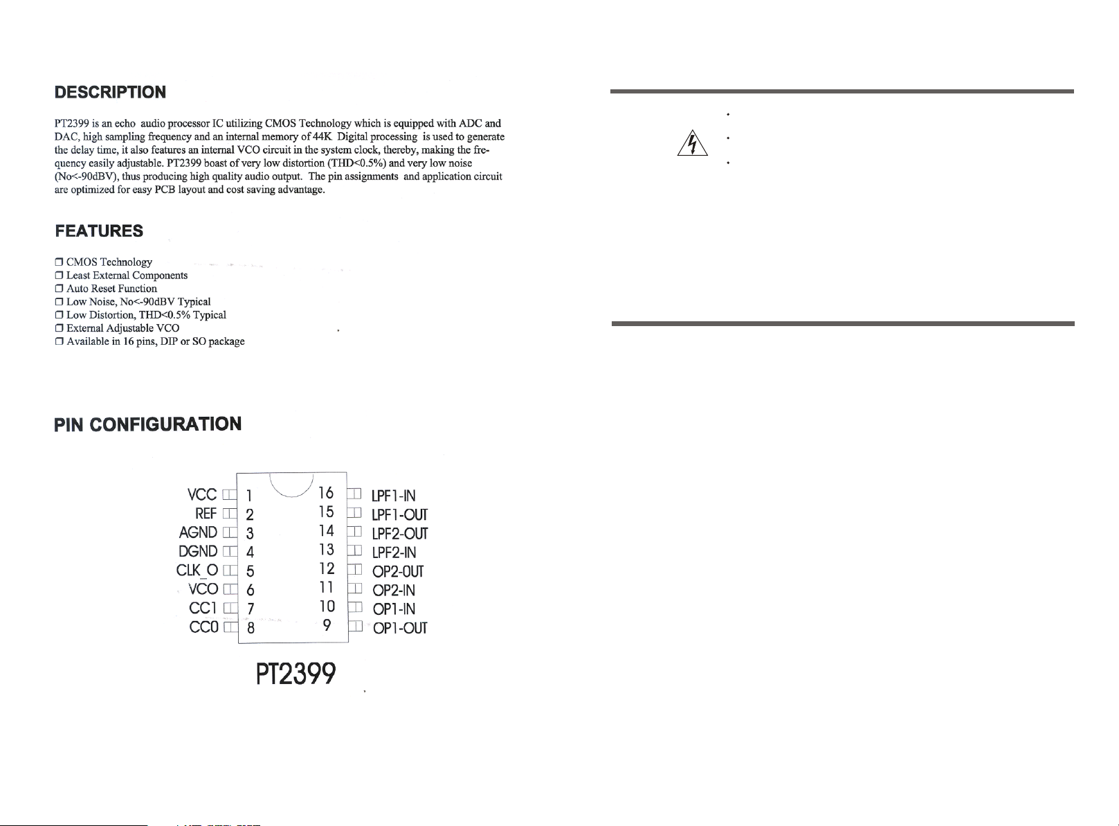
Echo IC Pt2399
CAUTIONS
CONTENTS
There is high voltage inside this unit. Make sure to pull out the plug of this unit before
repairing!
There are many high voltage components inside this unit. Please pay attention to all
warnings and instructions marked on this unit to avoid electric shock!
Specifications of the replaced components must be the same as that of the original
components. Do not change the components' specifications to prevent risks!
¢ñ
Cir cui t Makeup................................................................................................
Vol ume adj ust ment , sound f i el d pr ocess i ng and EQ adj ust ment ci r cui t s3. I nput si gnal s det ect , sear ch and f r equency s pect r um sampl i ng ci r cui t s. 4. Contr ol Ci r cui t .
1 INPUT PART.....................................................................................................2 ...................................................................................................................................5. Microphone Circuit............................................................................................6. Power Amplifi cation and Protection Circuit.........................................................
¢ò
.................................................................. I NSTRUCT I ONS TO THE CI RCUI TS
1. THE FRONT CONTROL PANEL.........................................................................2. THE MAIN AMP PART........................................................................................
¢ó
.................................................. THE E XPL ANATI ON FOR KEY COMPONENTS
CPU IC W78E54.............................................................................................. volume control IC M62446................................................................................ Echo lC Pt2399................................................................................................
1
1
3
3
4
8
10
12
12
16
24
24
25
27
- 27 -
Page 3

¢ñ Ci r cui t Makeup
1. INPUT PART
AV210 has three ways of the analog audio source input and one group of 5.1 channel input
jacks. Their switch is realized by the electronic switch. The circuit incorporates two kinds of
electronic switch IC: CD4052 (dual channel one out of four electronic analog switch) and
Cd4053 (trio channel one out of two electronic analog switch). Their real value tables are as
follows:
CD4052 REAL VALUE TABLE
X0 X1 X2 X3
A
B
0
0
0
1
0
1
1
1
There are still two important control signals SEL and SEL1 in this circuit. When SEL is
high level, the circuit is in the mode of 5.1 CH input from outside. When SEL1 is high
level, the circuit is in the cyber logic mode. When both of them are low level, the circuit
is in the Hi-Fi mode (direct mode) and the standard sound field processing mode. They
work in the following steps.
the pins 38 and 39 of the CPU N422 are added into the pins 9 and 10 of the electronic
switch N401. The electronic switch selects the input mode circularly from VCD, CD,
AUX and 5.1CH according to different combinations of levels A and B. It can be divided
into two modes: 5.1CH and three analog input modes. Their signals' flow is as follows:
1.1 5.1CH input mode: In this mode, A and B are high levels, L and R channel signals
are sent out from the pins 3 & 13 of N401. Then the levels reach IC N402 to be master
volume adjusted after amplified by N407A and N407B. At the same time, the pin 32 of
CPU N422 sends out a high level to the electronic switch N410's pins 9, 10 and 11 (SEL
control signal). C, SR and SL signals are sent out from the N410's pins 14, 15 and 4
to IC N402 where separate volumes are adjusted. SW signals (D-SW) is sent to the IC
N402's where the volume is adjusted. Therefore, the 6 channel signals of 5.1 CH input
are selected by the electronic switch and added into the electronic volume adjusting IC
where the separate volume adjustment is performed. Then the signals pass to the rear
circuit, the whole unit's input source is selected as 5.1CH input mode.
1.2 Three analog input mode: Press the INPUT button to select one of the VCD, CD
and AUX. The select function is performed when the control levels Aand B from the pins
38&39 of the CPU N422 are added to the pins 9&10 of the electronic switch N401. The
signals of L& R channels are sent out from the pins 3&13 and then amplified in the oper
ational amplifier N407A and N407B. AV210 incorporates three processing modes to the
signals: Hi-Fi, Cyber Logic and standard stereo. Their signal's flow is as follows:
1.2.1 Standard Stereo Processing Mode: The L & R channel signals from the N407A
and N407B are added to the IC N402 where the electronic volume is adjusted. At the
same time, a signal selected from the L channel passes N408A and N406B where the
signal is processed through low pass filter to obtain a subwoofer signal (S-SW). S-SW
is added to N411's pin 5 and the pin 9 (SEL) is low level. According to the real value
table, S-SW signal is sent out from the pin 4 to N402's pin 6 where the electronic volume
is adjusted. In this mode, this unit is in the three channel output mode.
When pressing the INPUT button, the levelsA and B from
CD4053 REAL VALUE TABLE
X B Y C
A
0
X0
X1 1
1
Z
0
Y0
Y1
0
Z0
Z1
1
- 1 - - 26 -
Page 4

1.2.1 Hi-Fi Processing Mode: The signal flow is the same as that of the standard stereo
mode. The electronic volume adjusting IC N402 shut off other audio channels under the
control of the CPU. Neither the sound fields processing and balance adjustment can be
performed. Therefore, S-SW cannot be sent out and the whole unit is in the two channel
output mode.
1.2.3 Cyber Logic: L&R channel signals sent out from N407A and N407B reach the IC
N402 where the electronic master volume is adjusted. Meanwhile, the signals selected
from the channel L passes through the low pass filter N408A where it is divided into two
lines. One line reaches the pin 13 of N411 through R657 and another line reaches the
pin 5 of N411 after it is amplified through the low pass filter N406B. The signal selected
from the channel R reaches the pin 1 of N411 after being amplified through the low pass
filter N408B. N411's pin 9 (SEL) is the low level. According to the real value table, the
S-SW signal sent out from the pin 4 is added to the pin 6 of N402 where the electronic
volume is adjusted. The pins 10&11 (SWLL) are high level. According to the real value
table, the central channel signal (S-C) sent out from the pin 14 of N411 and the surround
channel signal (S-S) sent out from the pin 15 of N411 are added to the pins 12, 2 and 5
of N410. (The S-S is divided into two signalssurround left and surround right.) At this
time, the pins 9, 10 and 11 (SEL) are low level. According to the real value table, these
three lines of signals sent out from the pins 14, 15 and 4 reach the IC N410 where the
volume is adjusted separately. This unit is in the six-channel output mode.
The relationship of all input source switches and sound processing mode is shown as
Figure 1.
volume control IC M62446
Press the INPUT
button to select
circularly
Three modes
input
5.1 CH input
Hi-Fi mode
Standard
Stereo
mode
Only L & R channel outputs,
Sound fields and
EQ settings are invalid
Only L,R & SW channel outputs,
Capable of setting the
Concert sound field and EQ
Cyber Logic
mode
(Figure 1)
6 CH output, capable of setting
the Theater sound field and EQ
6 CH output, capable of setting
the Theater sound field and EQ
- 2 -- 25 -
Page 5

2. Volume adjustment, sound field processing and EQ adjustment
circuits.
All channel signals are sent to N402 inside which the independent volume adjustment,
EQ adjustment and all sound field modes process are performed.
The sound field processing and EQ adjusting circuit is mainly processing the L&R
channel signals. According to the schematic diagram, the L&R channel signals are
added simultaneously to the pins 15, 17, 13 and 16 of N402. When the unit mode is in
the Hi-Fi mode, the internal circuit of the pins 17&16 is connected and the other input
signals are cut off. At this time, only the L&R channel volume can be adjusted and only
the pins 31&32 send out signals. Therefore, the unit is in the 2CH output mode. The
unit mode is not in the Hi-Fi mode, other input signals are connected but the pins
17&16 signals are cutoff. At this time, all channel volumes can be adjusted
independently and the sound field processing or EQ adjusting of the L&R channels
can be performed. Finally, all channel signals pass out from the pins 31, 32, 33, 34,
35&36. The SW channel signal from the pin 36 reaches the amplified speakers to be
amplified through the SW output terminals. Other channel signals reach to the power
amplifying circuit to be amplified. The L&R channel signals will go through 1 grade
LPF and MIX amplification (Karaoke signals are overlapped into L& R channels).
st
3. Input signals detect, search and frequency spectrum sampling cir
cuits
3.1 Input signals detect and search circuit: The six channel signal lines of the input IC
N402 are connected with 100K sampling resistors R533, R534, R657, R676 and R678
respectively. The signals are mixed by these resistors and added to the opposite-phase
input terminal to be amplified. VD431 and C481 connected to N403B's output end
constitute half-wave rectifying filter circuit. Then the signals reach the voltage comparer
composed of N403A. The output end of N403A (SEARCH)is connected to the pin 28 of
CPU. This control signal is the search and detect signal: when it is low level, it enters the
search mode; when it is high level, it stops searching. Its works as follows:
¢ó T HE E XP L ANA T I ON F OR KE Y COMP ONENT S
CPU I C W7 8 E5 4
3.1.1 When this unit is getting started, the A&B control signals from the pins 38&39 in
the domination of the CPU's inter program are added to the input select circuit to
search circularly once. When there are no signals in these four input connectors, the
VCD mode stops automatically. When there are signals in one of the four connectors,
AC signals will appear in all channels of the input N402. These AC signals are
amplified by N403B and rectified and filtered by VD434 and C481 to become DC
signals. At this time, the opposite-phase voltage of N403A is 0.01V. When this DC
voltage surpasses 0.01V, the output end of N403B sends out a high level (SEARCH)
close to positive power supply voltage (A+6V) which reaches the pin 28 of CPU. CPU
keeps searching in the connector in which there are input signals and the unit will play
normally.
1.2.2 When press the SEARCH on the front panel, CPU sends out A&B control
signals again to start searching. Meanwhile, the pin 27 (EX) sends out a high level
which makes V446 inductive. The emitter of V446 sends out a high level which passes
through R498 which makes the opposite-phase voltage of N403A to be 0.4V. That is
to say, if you want to stop searching of CPU, the gained voltage after the input signals
are rectified and filtered must exceed 0.4V. This voltage is higher than 0.01V when
this unit is getting started in order to avoid that the CPU receives signals mistakenly
and stops searching due to the large external interference signals. If the input signals'
amplitude is not high enough, CPU will continue searching. When the amplitude is
high enough, N403A sends out high level to the pin 28 to stop searching. The pin 27
(EX) will become low level again and the opposite-phase voltage of N403A will also
returns back to 0.01V. The whole searching process is finished.
- 3 - - 24 -
Page 6

3.2 Spectrum Sampling Amplification Circuit: The routes carrying the five-channel
signals sent from the IC N402 are connected to the sampling resistors R494, R495,
R496, R565 and R566 respetively.(The SW channel sends out the signals directly.) After
being mixed by these resistors, the signals reach N406A to be amplified. The incurred
spectrum analyzing signal source is sent to the front panel circuit.
To M62446
4. Control Circuit.
To 24C02
To CD4052
A
B
SCK
9
8
7
6
5
4
3
2
RR901
8*4.7K
1
C535
47u/16V
L406
100uH
D+5V
534
RelayT est (Y402)
R-T
R690
C525
223
RelayC o n tro l
To CD4053(N411)
E.OE
SEL1
4.7k
DIS1A
DIS1B
DIS1C
11X312X013X114X215
C(2)9B(1)10A(0)
8
100Hz
C523
R606
VD444
LM324
N418A
+12V
411
3
5.6K
R604
104
D+5V
N422
AT89C54
R680
4.7k
N420B
S-6.2V
2.2U
10K
R607
1K
1N4148
1
2
C521
683
10K
R603
P-RST
R687
1k
VD409
1N4004
R688
2.2k
R689
2.2k
+A6V
4.7V
VD410
C665
47u/16V
R686
1k
C531
10u/16V
R629
10k
16
S+6.8V
VDD
X41X62XCOM3X74X55INH6VEE7VSS
N419 4051
35Hz
300Hz
C526
2.2U
2.2u
C529
R617
1K
R616
VD446
1N4148
14
LM324
N417D
82K
R615
12
13
C527
154
5.6K
R614
10K
R613
10K
10K
R612
R611
1K
1N4148
VD445
14
82K
N418D
LM324
R610
C528
154
12
13
C524
223
5.6K
R609
10K
R608
SDA
CLK
DATA
4039383736353433323130
Vcc
P00(AD0)
P01(AD1)
P02(AD2)
P03(AD3)
P12
P13
P14
P10(T2)
P11(T2)
123456789
7
4558
5
6
100K
R618
C520
82K
N417C
-12V
683
R605
C522
5.6K
R599
To CD4053
LATCH
SEL
P07AD7)
P04(AD4)
P05(AD5)
P06(AD6)
P15
P16
P17
RST
1011121314151617181920
R624
D+5V
1K
R619
+12V
1KHz
2.2U
R602
1K
R601
VD443
1N4148
8
82K
LM324
R600
9
10
C518
682
10K
R598
Exchange Search Level
SEARCH
EX
XS4
29282726242322
ALE
PSEN
P27(A15)
EA/Vpp
P30(RXD)
P31(TXD)
P32(INT0)
P33(INT1)
V437
10K
VD448
N420A
4558
-12V
2
R621
680K
10K
682
C519
R594
o 2 Jog
ToEncoder ( Master )
To Encoder 1(Master VOL.)
A1B1A2
B2
123456789
25
P21(A9)
P22(A10)
P23(A11)
P24(A12)
P25(A13)
P26(A14)
P34(T0)
P35(T1)
P36(WR)
P37(RD)
XTAL2
G401
12M
C661
20P
2N5551
R623
10k
1N4148
R622
1K
1
8 4
3
C530
104
VD447
3.3V
10K
R620
3KHz
2.2U
C517
R597
R596
1K
VD442
1N4148
8
N418C
LM324
9
10
C515
5.6K
10K
R593
To uPD16311
MIC Mutting
REMOTE
CLK
DATA
STB
K-MUT
8PIN
SCK
SDA
R685
4.7k
R691
21
P20(A8)
GND
XTAL1
C662
4.7k
5
6
7
8
D+5V
SCL
SDA
VDD
TEST
N421
24C02
A01A12A23VSS
20P
C668
47u/16V
4
+12V +12V
C669
47u/16V
-12V -12V
The control circuit of this player is divided into CPU Circuit, Front Panel Control and
Display Circuit and Spectrum Analyzing Circuit.
4.1 CPU Circuit
N422 (AT89C540) is this unit's CPU which sends all commands to the commandcontrolled circuits to perform all control functions. It incorporates +5V power supply and
its pin 40 is the power supply pin. The 12M crystal oscillator provides the work clock for
itself. The pin 9 is the restoration pin. When this unit is getting started, +5V passes
VD409 to reach the positive pole of C531. Because of the C531's charging, its negative
end sends out an instantaneous high level which passes through R686 to reach the pin
9 of N422. The pin 9 of N422 restores the low level mode with the end of charging. This
restoration circuit's style is the high level restoration to keep in low level. You can also
refer to the circuit diagram for other command instructions.
The static information such as the power-on logo and on screen displays when this unit
is working is stored in the CPU's static memory. N421 is a power-off-mode memory which
can record the working information when this unit is turned off and call back these
information when this unit is turned on next time. Therefore, you need not to readjust the
unit every time you turn it on. Furthermore, the sound field modes that you set are also
stored in N421, which can be called back when needed.
4.2 Front panel control and display circuit
D+5V
VD450
1N4148
R628
VD449
1N4148
4.7K
B
+12V
2N5401
R627
5.6K
V436
E C
R626
V435
2N5551
2.2K
R625
16KHz
2.2U
C514
+12V
272
411
10K
R592
R591
1K
VD441
1N4148
1
N417A
LM324
3
2
C512
681
5.6K
R589
10K
R588
10K
82K
C516
R595
272
+12V
R570
1k
VD438
6.8V
27k
180k
470k
75k
R571
DIS2A
DIS2B
DIS2C
R572
R574
1K
S+6.8V
10KHz
C511
2.2U
R587
R586
1K
VD440
1N4148
7
82K
LM324
82K
N418B
-12V
C513
681
R590
R585
5
6
C509
152
5.6K
R584
10K
R583
R573
C505
47u/16V
10K
152
C510
DISPLAY
R579
10K
R581
C508
10u/16V
16
VDD
X41X62XCOM3X74X55INH6VEE7VSS
N416
10k
2.2k
R578
C507
10u/16V
1K
R580
5
6
N417B
7
11X312X013X114X215
C(2)9B(1)10A(0)
4051
C506
47u/16V
8
S-6.8V
4.3k
R576
R5771.5k
LM324
VD439
6.8V
1k
R575
-12V
R582
470K
This circuit incorporates an exclusive IC N901 (UPD16311). Its pins 10, 11, 12 and 13
are connected to the press scan matrix which receives the control commands from the
user and process them into two-line outputs: One line reaches to the VFD to display the
working modes, another line passes pins 5, 6, 8 and 9 to CPU to finish the control
functions.
N902 is the remote control sensor. It convert the infrared signals received to electric
signal and then send it to the pin 13 of CPU to finish the remote control function.
RP901 and RP905 comprise a digital pulse potentiometer. When rotating it, a series of
digital pulse will be sent out and added to the pins 23, 24, 25 and 26 to be detect and
processed to finish the control functions. RP901 finishes the master volume adjustment
and RP905 finishes multi-function adjustment.
- 4 -- 23 -
Page 7

4.3 Spectrum analyzing circuit (The flow chart is shown an Figure 2)
35HZ
100HZ
300HZ
1KHZ
3KHZ
10KHZ
N419
CD4051
Frequency
Selected
}
CPU
3
DISPLAY +
N416
CD4051
Automatic
Spectrum
Gain
Adjustment
3
N417B
-
-
}
7-band Filter
.
16KHZ
CPU
N420B
+5V
V436
+
-
.
A/D Conversion
N420A
V437
V435
CPU Pin 12
CPU Pin 1
(Figure 2)
4.3.1 Automatic spectrum gain adjustment circuit: In order to avoid that the display
amplitude is too narrow when the input signals are too weak or the whole display
appears when the input signals are too strong, this unit incorporates an automatic
spectrum gain adjustment circuit which employs a single channel 1-out-of-8 electronic
analog switch N416 (CD4051). Its real value table is below. Its working principle is
that it changes the opposite-phase ground resistor's resistance value of the
operational amplifier N417B to change the gain times.
We have mentioned before that the spectrum analyzing signal source is sent to the
operational amplifier N417B's in-phase input terminal to be amplified. Its amplified
times depend on the resistance value of the resistor connected through the electronic
switch N416 to the opposite-phase terminal. When the master volume is too big, the
CPU will automatically add the ground resistor's resistance value to reduce the am
plification times. When the master volume is too small, the CPU will automatically
reduce the ground resistor's resistance value to increase the amplification times.
CD4051Real Value Table
CD4051 Real Value Table
X0 X1 X2 X3
1
0
A
0
B
C 0
0
0 0 0
0
1
X4 X5 X6 X7
1
0
1
0
1
0 1
1
1
1
0
1
1
1
V444
C
SR
E.O.E
VD418
6.8V
VD411
6.8V
C441
VD419
47u/25V
V430
100k
10k
R485
R484
VD417
1N4148
VD415
C9014
V426
+36V
V408
R692
220/0.5W
R413
104
C402
C401
C9015
R483
10k
SPEAKER
L
47k
R478
1N4148
L401
0.7uH
C435
V411
C4467
2N5551
R418
R417
V407
2N5551
V404
2N5401
200
C408
33
R411
33K
V402
R406
2.7K
2.7K
R405
V401
100u/50V
R473
1u/16V
2.7k
R472
3.9k
R470
R424
R425
0.25/3W
0.25/3W
R421
R420
100/0.25W
10
33K
R419
10
V405
2N5551
R414
R415
2K
4.7K
104
C409
1K
R410
2N5551
C407
100U/16V
47
R408
47
R407
2N5551
C406
221
47K
R404
C405
10u/16V
1K
R403
R402
470k
10k
R401
L
1N4148R487
1526374
1k
Y402
R497
RE-402DM
9
101112
10K
C-OUT
SR-OUT
9014
V431
R479
4.7/1W
C436
R471
100/0.25W
R412
V441
S8050
R486
10k
C440
220u/25V
C439
220u/25V
10k
R481
V429
C9014
10k
R480
1k
V428
C9014
V427
C9014
VD416
104
V406
V403
1N4148
-36V
3.9k
V412
10
R423
R422
10
2N5551
1k
VD401
2N5551
+36V
A1694
V410
2N5401
V409
2N5401
200
R416
1N4148
VD402
R409
620
C404
C403
V423
2N5551
V420
V419
R693
220/0.5W
R694
220/0.5W
200
R440
1N4148
R438
R433
R432
104
C411
100u/50V
100U/50V
9014
SL
V445
C8050
MUT2
R-T
+36V
8
14
1N4148
VD412
13
Y401
SL-OUT
R482
47k
C437
1u/16V
3.9k
R474
C4467
10
R445
R444
10
2N5551
V416
2N5401
C418
33
33K
V414
2N5551
2.7K
2.7K
C412
104
V413
2N5551
C415
10u/16V
R430
V442
S8050
R426
GSADC12V
R681
10
C442
+16V
2200u/25V
VD421
SPEAKER
R
FL401
L402
0.7uH
R477
4.7/1W
2.7k
R476
R475
0.25/3W
R452
R451
0.25/3W
R448
100/0.25W
R447
100/0.25W
R446
33K
V417
2N5551
V418
R441
2K
4.7K
R442
1k
R439
104
C419
1K
R437
C417
100U/16V
R435
47
47
V415
R434
C416
221
47K
R431
1K
R427
470k
10k
V440
2N5401
R
V443
C8050
V432
-36V
VD420
C443
2200u/25V
10
R488
RL254
VD422
RL254
VD423
T4A/250V~
104
C438
-36V
3.9k
A1694
V424
2N5401
10
R450
R449
10
V421
2N5401 V422
2N5551
R695
220/0.5W
200
R443
VD405
1N4148
VD406
1N4148
R436
620
C414
104
2N5551
C413
100U/50V
R429
10k
R428
4.7k
+12V
C455
9014
1N4148
R489
-16v
RL254
VD424
FL402
T4A/250V~
MUT1
104
C453
47u/16V
3
C452
2
OUT
7812
GND
N412
IN
1
C450
470u/25V
560/1W
R490
560/1W
R491
220/3W
C447
6800u/50V
C446
VD425
1N5404
VD426
1N5404
RL254
C444
224
FL403
T6.3A/250V~
XS3
6P1N
R684
47k
4
53
N415
TDA2030
1
103
C460
R683
47k
4
53
N414
TDA2030
1
SL-INC-IN SR-IN
C424
10u/25V
C-OUT SL-OUT SR-OUT
R682
47k
4
53
+16V
N413
TDA2030
1
-12V
C456
104
47u/16V
C454
47u/16V
104
6
R467
2
R463
2
R459
2
V433
12V
R493
2k2
VD429
C451
470u/25V
R492
220/3W
C449
6800u/50V
FUSE
C448
104
VD427
1N5404
VD428
1N5404
C445
224
FL404
T6.3A/250V~
12345
C433
10
104
2.2k
R466
15k
R455
151
C432
C430
R465
680
104
C428
10
2.2k
15k
R462
R454
151
C427
C431
R461
680
C426
C423
104
10
2.2k
R458
15k
R453
151
C422
C429
22u/16v
R457
680
TO saitchp wero ob ard
1
2
XS2
2PIN
C457
S8550
~275V104
C
D
L403
1.8mH
A
B
T3.15AL250V
2
XS1
2PIN
1
2
XP1
2PIN
50Hz 1
~220V
22u/16V
C434
103
22u/16V
10u/25V
-16V
- 5 - - 22 -
Page 8

SCHEMATIC DIAGRAM OF THE MAIN AMP BOARD
S-C
S-S
150
MUT2
R501
SR-IN
SL-IN
C-IN
R496
47k
R495
47k
R494
47k
D+12V
WBC
R549
150
VD436
C497
100u/16V
D+5V L405
R500
22k
R676
100k
X012X113Y02Y11Z05Z13INH6A11B10C
N410
R6671kR668
D-SW
47k
R502
R503150
SW
SW
LINE OUT
R552
47k
R551
47k
R550
5.1V
47k
CLK
DATA
LATCH
L404
100uH
C496
47u/16V
100
100
R546100
R547
R548
C495
104
38
39
40
41
42
CLK
DATA
DVDD
LATCH
M62446
OUT41OUT32OUT23OUT14AVDD5SWIN6GNDS7SRIN8SLIN9GNDC10CIN11GNDR12RIN13GNDL14LIN15BYPASR16BYPASL17LTRE18LBASS319LBASS220LBASS1
N402
C468
104
4.7u/16V
MUT1
C469
R663
C666
A+6V
47u/16V
R677
100k
R678
100k
R675
100k
A+6V
A-6VSEL
7Z4Y15X14
16
8
Vss
VEE
VCC
CD4053C
9
1k
1k
R5071kR510
R5061k
R50447k
R50547k
R50847k
R50947k
C
SR
33P
C502
R559
C501
103
101
R553
10k
C498
-12V
4.7u/16V
4.7u/16V
4.7u/16V
4.7u/16V
C494
C493
C492
C491
33
34
35
36
AGND37DGND
SLOUT
SROUT
SWOUT
4.7u/16V
4.7u/16V
C470
C471
100k
100k
R665
100k
R664
+12V
470
R529
R535
C467
47u/16V
6.8V
VD431
C462
47u/16V
C461
104
R5111k
R51247k
R51347k
SL
VCD R
N404B
22k
R560
N404A
2
R554
4.7u/16V
C490
C472
R666
47
168
A+6V
1k
R514
VCD L
R
7
4558
5
6
10k
R561
22k
1
4558
C499
3
10k
A-6V
4.7u/16V
C489
29
31
AVSS30LOUT
ROUT32COUT
C473
4.7u/16V
100k
R536
R
1k
R531
V4382N5551
X13Y
X012X114X215X311Y01Y15Y22Y3
1k
R51647k
R515
CD R
103
101
8 4
C500
+12V
R555
C667
47u/16V
C487
104
C486
4.7u/16V
4.7u/16V
C4744.7u/16V
100k
R537
L
R532
3
N401
CD4052
R5181k
R51747k
L
7
N405B
4558
33P
R562
22k
C503
10k
R563
4558
N405A
10k
R556
2
-12V
R557
47k
C484
822
24
25
27
C485
4.7u/16V
CL228CL1
CR226CR1
RTRE
C475
822
C476
C477
4.7u/16V
4.7u/16V
100k
1k
A
B
6A10B9
INH
VEE
4
7
47k
R5221kR5191k
R520
R52147k
CD L
TAPER
101
5
6
C504
R564
22k
1
8 4
3
+12V
10k
R558
47k
N403A
A+6V
84
R542
100k
C483
153
C482
334
C481
RBASS122RBASS223RBASS3
VD434
C539
4558
21
N403B
153
334
C478
C479
5
-12V
C488
470
R530
47u/16V
R545
6.8V
VD432
C463
104
C464
47u/16V
A-6V
1k
R5231k
R52447k
R52547k
R526
5.1CHL
5.1CHR
TAPEL
4.3.2 Frequency Selected Circuit
The signal amplified by the N417B is coupled by C508 and then sent to the 7-band
filter composed of the operational amplifiers. Setting its feedback capacitor's capacity
can define the corresponding frequency amplitude. The frequency value marked on
their output points is the frequency band's central frequency. There's a half-wave
rectifying circuit connected to the every band filter's output end. The circuit will rectify
R566
47k
47k
R565
3
2
N406A
4558
8 4
22k
R567
-12V
+12V
1
DISPLAY
SEARCH
R544
4.7k
1k
R543
1
4558
3
2
R541
220
4.7u/16V
10k
R540
R539
150
1N4148
R568
10k
10u/16V
7
R538
1.5M
6
100k
R533
100k
R534
MIC
MS
D+5V
8
XS5
A-6V
R498
2.2k
9014
V446
R499
A+6V
EX
101
C480
680k
R679
75k
R659
C646
+12V
-12V
1234567
8PIN
ToVFD Board
S-C
N411
X012X113Y02Y11Z05Z13INH6A11B10C
4.7k
1k
R6571kR655
C648
10u/16V
R662
100k
47k
R661
C647
103
R660
47k
5
6
N406B
4558
682
7
S-SW
S-S
A+6V
A-6V
7
4Y15X14
16
8
Z
Vss
VEE
VCC
CD4053C
9
SEL
1k
D-SW
R658
SEL1
the amplified AC signals into the DC voltage. The circuit is mainly performing the
frequency sampling function which can show the amplitude of every frequency of the
whole audio signals through the DC voltage. If the low frequency of the current audio
signals is strong, the DC voltage of the 35Hz and 100Hz band filter is higher. If the
high frequency is strong, the DC voltage of the 10K and 16K band filter is higher. The
output end of these seven band filters is connected to seven input terminals of the
electronic switch N419 (CD4051). CPU will send commands to make this electronic
switch select the frequencies circularly (Refer to the above real value table). The
output terminal of the pin 3 of N419 will send out a series of voltage representing the
corresponding frequency's amplitude.(See Figure 3)
V
35HZ
100HZ
300HZ
1KHZ
3KHZ
10KHZ
16KHZ
Note:the diagram's
voltage amplitude
is not definite
35HZ
T
Switch interval
Frequency selected circularly period
L
47
2N5401
V439
C465
10u/16V
C466
10u/16V
47k
R528
R527
47k
REC L
REC R
1
N408A
4558
-12V
47k
101
C642
R641
3
2
56k
R640
R639
1
4558
N407A
C420
47u/16V
C421
3
2
-12V
C538
7
R
4558
+12V
N408B
8 4
75k
C643
101
5
6
R645
56k
56k
56k
47u/16V
8 4
C639
221
R636
100k
4.7u/16V
R635
100k
75k
R642
R643
R644
7
4558
N407B
+12V
C641
221
5
6
R638
100k
C640
4.7u/16V
R637
100k
(Figure 3)
- 6 -- 21 -
Page 9

4.3.3 A/D conversion and display output circuit: The output voltage from the pin 3 of
127
CONNECTION
CORDS
¦µ
0.6 SHAPED 10mm
W4,W6,W7,W9,W13,W17,W23,W25,W29,W31,W32,W35,
W40,W41,W44~W47,W54,W55,W62,W65,W80,W90,W97,
W103,W111,W112,W117,W121,W122,W133,W137,W142,
W143,W154,W163,W167,W168,W174,W177,W178,W180,
W181,W185,W186,W190,W207,W208,W209,W37
128
CONNECTION
CORDS
¦µ
0.6 SHAPED 12.5mm
W57,W60,W67,W68,W70,W71,W77,W93,W104,
W120,W123,W124,W128,W130,W131,W144,W145,W148,
W204
129
CONNECTION
CORDS
¦µ
0.6 SHAPED 15mm
W83,W85,W86,W107,W115,W126,W129,W146,W147,
W169~W173,W175,W176,W182,W183,W191,W201,W82
130
CONNECTION
CORDS
¦µ
0.6 SHAPED 20mm
W33,W34,W48,W51,W114,W132,W134,W141,W166,W192,
W196,W200,W203
131 CABLE
20# 60mm BLACK WITH CHIP
SOLDER
GROUND WIRE
132 CABLE 18# 70mm BLACK
XJ1~XJ2
CABLE
22££ 80mm BLACK
XJ1~XJ2
133 FUSE TUBE T6.3AL 250V FL403,FL404
134 FUSE TUBE T4AL 250V FL405,FL401,FL402
135 FUSE HOLDER BLX-2 FL405
136
RADIATOR
BOARD
30×16×16 AB207
SRQ401
137
LARGE
RADIATOR
267.5×91×70 AV210
CONNECTED TO THE MAIN AMPLIFICATION BOARD
138 FUSE HOLDER 0
FL401~FL404
139 SMALL CHIP AB207
FIX TRIODE
140
ANGLE
ALUMINUM
90×23.2×30 AV210
POWER IC / LARGE RADIATOR
141
TAPPING
SCREW
BT 3×8 BLACK
2 FOR RADIATOR BOARD/MAIN AMPLIFICATION BOARD,
1 FOR N412/RADIATOR BOARD
142
TAPPING
SCREW
PB 3×12H COLOR ZINC
2 FOR SMALL CHIP/LARGE RADIATOR, 5 FOR ANGLE
ALUMINUM/LARGE RADIATOR
143
TAPPING
SCREW
PWT 3×8×8 COLOR ZINC
1 FOR MAIN AMPLIFICATION/RADIATOR, GROUNDED
144
TAPPING
SCREW
BT 3×8H COLOR ZINC
1 FOR MAIN AMPLIFICATION/RADIATOR, 3 FOR ANGLE
ALUMINUM/POWER IC
145
MACHINE
SCREW
PWM 3×16×8 COLOR ZINC
4 FOR POWER TUBE/LARGE RADIATOR
146 SCREW NUT M3
147
SCREW
SPACER
¦µ
3×7.2×0.5
148
SPRING
SPACER
¦µ
3
149
INSULATION
RING
¦µ
3×6×3
N413~N415
150 MICA SPACER
18×13×0. 1
151 MICA SPACER
22×19×0. 1
4 FOR POWER TUBE / RADIATOR
N419 passes through N420B where it is amplified and sent to the opposite-phase
terminal of N420A. N420A composes a voltage comparer. We'll discuss its detailed
working process according the voltage comparing characteristics (When the in-phase
end's voltage is higher than that of the opposite-phase end, the output is the positive
power. When the in-phase end's voltage is lower than that of the opposite-phase end,
the output is the negative power.) and the figure 4.
When the opposite-phase end has a DC voltage representing 35Hz signal amplitude,
the output of N420A is a low level close to the negative power supply. At the same time,
+5V provides conditions for V436 to be conductive and a high level from the collector
of V436 charges C530. The positive end's voltage of C530 (i.e. the in-phase end of
N420A) is increasing gradually. When the voltage reach that of the opposite-phase
end, the voltage comparer will overturn. Therefore, N420 sends out a high level close
to the positive power supply voltage. When the comparer overturns, CPU will
terminate the 35Hz level selection and switch to the next frequency 100Hz. During the
switch interval, an instantaneous high level from the pin 1 of CPU makes V435
conductive and the voltage of C530 will be released. The in-phase end of N420A will
be charged from 0 level to 100Hz. When 100Hz charge is finished, it will switch to the
next frequency. The process is circulated under CPU's control. The charging time from
the 0 level to overturn represent current frequency's signal amplitude. The amplitude
is large, time is longer; the amplitude is small, time is shorter. We can conclude from
the above circuit working process: An analog series of DC level which has concrete
voltage value originally becomes two mode of 0 and 1. Its time period represents the
digital pulse of the original information. That is to say, it finishes the analog-to-digital
conversion process. The digital pulse sent out from the output terminal of N420A
reaches the pin 12 of CPU after opposite-phased by V437. And then CPU processes
it and sends it to front panel display IC N901 which will make dynamic spectrum
display on the display. As a matter of fact, every frequency is displayed sequentially.
However, what we see on the display screen is the working process all the spectrums
are displayed simultaneously due to every frequency display circulate very quickly.
V
100HZ
35HZ
Switch time interval
T
(Figure 4)
Charge time Charge time
- 7 -
V
35HZ
High level
discharge
100HZ
T
- 20 -
Page 10

92
VOLTAGE
REGULATOR
DIODE
5.1V 1/2W VD436,VD411
93
VOLTAGE
REGULATOR
DIODE
12V 1/2W VD429
94
VOLTAGE
REGULATOR
DIODE
6.8V 1/2W VD431,VD432,VD438,VD439
95 TRIODE 2N5401 V404,V409,V410,V416,V421,V422,V440,V436,V439
96 TRIODE 2N5551
V401,V402,V403,V405~V408,V413,V414,V415,V417~V420,
V435,V437,V438
97 TRIODE 8050C V432,V445,V441,V442
99 TRIODE 9014C V426~V429,V431,V443,V444,V446
100 TRIODE 9015C V430
TRIODE S8550D V433
101 TRIODE KB688O V412,V424
TRIODE KB688Y V412,V424
102 TRIODE KD718O V411,V423
TRIODE KD718Y V411,V423
103 IC LM324N DIP N417,N418
104 IC NJM4558D DIP N403~N408,N420
IC 4558C DIP N403~N408,N420
105 IC
L7812CV GOLD-SEALED TO220
N412
IC
LM7812 GOLD-SEALED TO220
N412
106 IC CD4051 DIP N416,N419
107 IC CD4053BCN DIP N410,N411
108 IC CD4052BCN DIP N401
109 IC M62446FP SOP N402
110 IC 24C02 DIP N421
111
IC
LM1875T T05B N413,N414,N415
112
SOFTWARE
PROGRAM CPU
CPU-AV210(RU)-0 N422
113
CRYSTAL
OSCILLATOR
12.00MHz 49-U G601
114 RELAY
JH1806-012-(3H1£«1Z1) DC12V
Y402
115 RELAY JH4237-012-2H DC12V Y401
116
PCB
4210-3
117
TERMINAL
SOCKET
AV6-8.4-53
XC401
118
TERMINAL
SOCKET
AV8-8.4-62
XC402
119
TERMINAL
SOCKET
AV1-8.4-5 BLACK
XC403
120 SOCKET 8 PINS 2.5mm XS5
121 SOCKET 9 PINS 2.5mm XS4
122 SOCKET 2 PINS 7.92mm XS1,XS2
123 SOCKET 6 PINS 3.96mm XS3
124
CONNECTOR'S
SOCKET
WP4-10A
XL401
125
CONNECTOR'S
SOCKET
WP6-10A
XL402
126
CONNECTION
CORDS
¦µ
0.6 SHAPED 7.5mm
W1~W3,W5,W8,W10~W12,W14~W16,W18~W22,W24,
W26~W28,W30,W36,W38,W39,W42,W43,W49,W50,W52,
W53,W56,W58,W59,W61,W63,W64,W66,W69,W72~W76,
W78,W79,W81,W84,W87~W89,W91,W92,W94~W96,
W98~W102,W105,W106,W108~W110,W113,W116,
W118,W119,W125,W127,W135,W136,W138~W140,
W149~W153,W155~W162,W164,W165,W179,W184,
W187~W189,W193~W195,W197~W199,W205,W206
- 19 -
5. Microphone Circuit
The microphone circuit is divided into two parts: The Front Process Section and Echo
Process Section
5.1 Front Section Circuit: Mainly performing volume adjusting/amplifying/modifying
function. The flow chart is shown as Figure 5.
MIC1
RP901
RP902
MIC2
N903A
N903B
V901
Following
Amplification
N904A
(Figure 5)
N904B
Voiced
Circuit
Echo
Process
Section
- 8 -
Page 11

5.2 Echo Process Section
59
PORCELAIN
CAPACITOR
50V 683 ±10£¥ 5mm
C521,C522
60
PORCELAIN
CAPACITOR
50V 154 +80%-20% 5mm C527,C528
PORCELAIN
CAPACITOR
100V 104±20£¥5mm
C412,C414,C402,C404,C458,C459,C434,C460
61
TERYLENE
CAPACITOR
100V 104 ±10% 7mm C423,C428,C433,C436,C438
62
TERYLENE
CAPACITOR
100V 224 ±10% 8mm C444,C445
63
TERYLENE
CAPACITOR
100V 472 ±5% 3.5mm C646
TERYLENE
CAPACITOR
63V 104 ±5% 5mm C446,C448
64
METAL
POLYESTER
FILM
CAPACITOR
CL21X 63V 153 ±5% 5 C478,C483
65
METAL
POLYESTER
FILM
CAPACITOR
CL21X 100V334±10% 7.5 C479,C482
66
METAL
POLYESTER
FILM
CAPACITOR
CL21X 100V 104 ±10£¥ 5
C530
67 CD CD11 16V10U±20%5×11 2 C465,C466,C507,C508,C531,C405,C415,C539,C648
CD
CD11 25V10U±20%5×11 2 C465,C466,C507,C508,C531,C405,C415,C539,C648
68 CD CD11 16V22U±20%5×11 2 C427,C432,C422
69 CD CD11 16V47U±20%5×11 2
C420,C421,C464,C462,C467,C488,C505,C506,C535,C452
C666~C669,C453,C454,C496,C665
70 CD CD11 16V100U±20%6×12 2.5 C407,C417,C497
71 CD CD11 50V2.2U±20%5×11 2 C511,C514,C517,C523
72 CD CD11 50V4.7U±20%5×11 2 C424,C426,C670,C671
73 CD CD11 25V100U±20%6×12 2.5 C441
74 CD CD11 25V220U±20%8×12 3.5 C439,C440
76 CD CD11 35V470U±20%10×20 5 C450,C451
77 CD CD11 50V100U±20%8×12 3.5 C403,C413,C401,C411
78 CD CD11 16V1U±20%5×11 2 C435,C437
79 CD CD11 16V4.7U±20%5×11 2 C469~C476,C481,C485,C486,C489~C494,C538,C640
CD CD110 35V3300U±20%16×35 7.5 C442,C443
CD CD11C 50V2.2U±20%4×7 1.5 C520,C526,C529
80 CD LUA 50V6800U±20%30×50 10 C447,C449
83
MAGNETIC
BEADS
INDUCTANCE
W4B WBC 6×10-1.5T L405
MAGNETIC
BEADS
INDUCTANCE
100UH ±10% 0410 VERTICAL
10mm
L404
INDUCTANCE
47UH ±10% 0410 VERTICAL
10mm
L406
84
INDUCTANCE
COIL
0.7UH SC-0.8×8.0×11.5 L401,L402
85 CHOKE COIL UU10.5-1.8mH L403
86 DIODE 1N4004 VD409
87 DIODE 1N4148
VD440~VD446,VD448,VD449,VD450,VD401,VD402,VD405,
VD406,VD415~VD417,VD419,VD420,VD434,VD412
88 DIODE RL254 VD421~VD424
89 DIODE 1N5404 VD425~VD428
90
VOLTAGE
REGULATOR
DIODE
3.3V 1/2W VD447
91
VOLTAGE
REGULATOR
DIODE
4.7V 1/2W VD410
The flow chart is shown as Figure 6. The front section signal is divided into three lines:
One line is sent by R980 and C958 to N403B's opposite-phase end. This line is just the
signal search and detect circuit we have mentioned before. When the front section
circuit of the microphone has signal output, the auto-search mode will be stopped.
Another line of signal is sent directly after being coupled by R946 and C926. This line is
the stereo channel of the echo channels. The third line is the feedback channel which is
coupled by R947, C927, C928 and R948 and then sent to the echo process IC N905's
16 pin. The line is LPF amplified and digitally delayed and then sent out from the pin 14.
The RP 903 connected to the pin 6 is the echo delay adjustment potentiometer. The pin
14's signal is coupled by R951 and R952 into two lines: I¢Ùt i s coupl ed by t he C932 and
R976 and f ed back t o t he i nput t er mi nal of t he pi n 16. I ¢Út i s coupl ed by C942 & R960
and i t s echo l evel i s adj ust ed by RP904. Then i t i s ampl i f i ed by t he ampl i f i cat i on ci r cui t
composed by V902. The ampl i f i ed si gnal i s sent out f r om t he col l ect or of t he V902 and
t hen coupl ed by R968 and C946. Fi nal l y t he si gnal mi xes wi t h t he st er eo channel si gnal
and makes up of a compl et e Kar aoke si gnal . Thi s Karaok e si gnal i s sent out t o t he
opposi t e- phase t er mi nal of N404B and over l aps wi t h L&R channel s. Then t he mi xed
si gnal r eaches t he power ampl i f i cat i on ci r cui t t o be ampl i f i ed. The Kar aoke si gnal
out put end i s al so connect ed t o t he mut e swi t ch i nsi de t he mi cr ophone socket . When
t he mi cr ophone i s not i nser t ed, t he cont act chi p i s gr ounded and t he mi cr ophone ci r cui t ' s
noi se i s f i l t er ed by t he shor t ci r cui t . When t he mi cr ophone i s i nser t ed, t he cont act chi p i s
cut of and t he mi cr ophone ci r cui t has nor mal out put .
th
N904B
OK¡ªMUTE
.
RP903
.
RP904
V902
AMP
N905
PT2399
Echo
Processing
.
Automatic
Search & Detect
Circuit
- 9 -
.
N404B
N405B
Mix with
the channels
L & R
(Figure 6)
¡¢
- 18 -
Page 12

30 CD CD11 25V220U±20%8×12 3.5 C415,C416
31 CD CD11 35V470U±20%10×20 5 C423,C424
32 CD CD11 50V1U±20%5×11 2 C411,C412
33 CD CD11 50V10U±20%5×11 2 C435,C436,C437,C438,C417
34 CD CD11 35V47U±20%6×12 2.5 C439,C440,C441,C442
35 CD CD11 35V100U±20%8×12 3.5 C418
36 CD
LUA 35V6800U±20£¥30×45 10
C421,C422
37 DIODE 1N4004 VD407,VD408,VD419
38 DIODE 1N4148 VD401~VD406,VD418
39 DIODE 1N5404 VD410~VD413
40
VOLTAGE
REGULATOR
DIODE
12V 1/2W VD415,VD414,VD409
41
VOLTAGE
REGULATOR
DIODE
6.8V 1/2W VD417,VD416
42 TRIODE 2N5401 V404,V408,V414,V418,V429,V431,V433
43 TRIODE 2N5551
V401,V402,V403,V405,V407,V411~V413,V415,V417,
V428,V430,V432
44 TRIODE 9014C
V406,V416,V421,V422,V423,V424,V426,V427,V434,V4
35
45 TRIODE 9015C V425
46 TRIODE KB688O V410,V420
TRIODE KB688Y V410,V420
47 TRIODE KD718O V409,V419
TRIODE KD718Y V409,V419
48 IC CD4052BCN DIP N401
49 RELAY JH4237-024-2H DC24V Y401,Y402
50 PCB
4217£-3
51
TERMINAL
SOCKET
AV6-8.4-3B XC2
52
TERMINAL
SOCKET
AV4-8.4-3B XC1
53 SOCKET 3 PIN 2.5mm XS3,XS4
54 SOCKET 6 PIN 2.5mm XS5
55
SOCKET FOR
EXTERNAL
CORDS
WP6-1B XL1
56 POLE SOCKET WP4-10A XC3
57
CONNECTION
CORDS
¦µ
0.6 SHAPED 7.5mm
W29,W32,W35,W36,W39,W48,W54,W58,W13
58
CONNECTION
CORDS
¦µ
0.6 SHAPED 10mm
W10~W12,W15,W19~W21,W27,W31,W33,W34,
W37,W43,W44,W47,W51,W53,W55
59
CONNECTION
CORDS
¦µ
0.6 SHAPED 12.5mm
W14,W16,W49,W50,W56
60
CONNECTION
CORDS
¦µ
0.6 SHAPED 15mm
W5,W7,W17,W18,W22,W23~W26,W28,W30,W45,W46
,
W40,W41,W52
61
CONNECTION
CORDS
¦µ
0.6 SHAPED 20mm
W38,W42,W57
62 FUSE TUBE T6.3AL 250V FL401,FL402
63
LARGE
RADIATOR
204×80×61 AB217 CONNECT TO THE MAIN AMP BOARD
64 FUSE HOLDER 0 FL401,FL402
65 SMALL CHIP AB207 FIX THE TRIODES V406 AND V416
66 TAPPING SCREW PB 3×12H COLOR ZINC 2 FOR SMALL CHIP AND LARGE RADIATOR
67 TAPPING SCREW PWT 3×8×8 COLOR ZINC 2 FOR PCB/RADIATOR
68
MACHINE
SCREW
PWM 3×16×8 COLOR ZINC 4 FOR POWER TUBE / LARGE RADIATOR
69 SCREW NUT M3 POWER TUBE SCREW
70 SCREW SPACER
¦µ
3×7.2×0.5
POWER TUBE SCREW
71 SPRING SPACER
¦µ
3
POWER TUBE SCREW
72 MICA SPACER 24×20×0.1 4 FOR POWER TUBE / LARGE RADIATOR
- 17 -
6. Power Amplification and Protection Circuit
6.1. Channels L&R Power Amplification Circuit: The L&R power amplifier employs
separate components. Taking the L channel as an example, its construction is shown
in Figure 7.
L Input
V440
V441
Mute
Compound
AC Negative
Feedback
R419,R410,C407
Differential
AMP Section
V401,V402
Constant Source
V403,V406,VD401,VD402
Mirror Image
Voltage
AMP
Section
V404
Power AMP (NPN)
V407,V408,V411
.
Power AMP (PNP)
V409,V410,V412
(Figure 7)
Temperature
Compensation
Section
V405
Compound
.
Speakers
The L channel signal is sent to the power amplification section by the electronic volume
adjusting circuit. A mute circuit installed in the input end. When press the MUTE button
on the remote control, a high level mute command is sent from the pin 1 of the electronic
volume adjusting IC N402. It makes V440 and V441 conductive to finish the mute control
function.
The L channel signal is coupled by the R403&C405 and sent to the base of the differential
AMP section V401. V401 and V402 compose the single-end input/output differential
amplification circuit. The audio signal is sent from the collector of V401 to the base of the
voltage amplification section V404 where its voltage is amplified and sent to the
compound power amplification section. V403, V406, VD401 and VD402 compose mirror
image constant circuit. VD401 and VD402 provide constant base current for V403 and
V405. V403's emitter resistor defines the current of the differential amplification section.
V406's emitter resistor defines the current of the voltage amplification section.
V407, V408 and V411 make up the NPN of compound power amplifier. V407 and V408 are
parallel connected. Their function equals a triode (able to amplify power). Then they mix
with V411 to constitute NPN compound tube (capable of enhance amplification times).
V409, V410 and V412 constitute the PNP of the compound amplifier. Its circuit
construction is the same as NPN. The temperature compensation section V405 has two
functions in the circuit: First it is a biasing of the NPN and PNP. Its working status defines
the static working current of the compound power amplification section. That is to say,
we can adjust the inductance degree of V405 to define the static working point of the
compound power amplification section. The usual way is to adjust the base resistor of
V405. It can also automatically adjust the working status of the compound power
amplification section when the temperature rises.
6.2 C, SR and SL power amplification circuit: These three channels employ the
exclusive power amplifier IC LM1875 (or TDA2030). It has five pins and is a good power
amplifier IC. The application circuit is very simple. It has 15W power output in the rated
condition. The pins 5 & 3 are the positive/negative power supplying pins and employ
2¡À2V. The pi n 1 i s t he si gnal i nput t er mi nal . The pi n 2 i s t he f eedback i nput t er mi nal .
The pi n 4 i s t he out put t er mi nal .
- 10 -
Page 13

6.3 Protection circuit: This unit incorporates the power-saving function. The L/R
NO. DESCRIPTION SPECIFICATIONS/PART NO. LOCATION SPECIFICATIONS
1
CARBON-FILM
RESISTOR
1/6W10¦¸±5% SHAPED 7.5
R417,R418,R422,R423,R444,R445,R449,R450
2
CARBON-FILM
RESISTOR
1/6W100¦¸±5% SHAPED 7.5
R546~R548,R541
4
CARBON-FILM
RESISTOR
1/6W1K±5% SHAPED 7.5
R506,R507,R510,R511,R514,R515,R518,R519,R522,R523,
R526,R529~R532,R543,R655,R657,R658,R667,R403,
R410,R430,R437,R412,R439,R479,R580,R586,R591,R596,
R601,R606,R611,R616,R619,R622,R626,R570,R575,R686,
R497,R457,R461,R465
5
CARBON-FILM
RESISTOR
1/6W1.5K±5% SHAPED 7.5 R577
6
CARBON-FILM
RESISTOR
1/6W2.2K±5% SHAPED 7.5 R625,R578,R689,R493,R498
7
CARBON-FILM
RESISTOR
1/6W4.7K±5% SHAPED 7.5
R544,R628,R499,R690,R685,R691,R428,R576,R587,R607,
R602,R612,R617,R592,R597,R480,R483,R453,R454,R455
8
CARBON-FILM
RESISTOR
1/6W5.6K±5% SHAPED 7.5 R584,R589,R594,R599,R604,R609,R614,R627
9
CARBON-FILM
RESISTOR
1/6W10K±5% SHAPED 7.5
R581,R583,R588,R593,R598,R603,R608,R613,R620,R623,
R624,R579,R629,R540,R554,R557,R560,R563,R487,R481,
R485,R553,R556,R401,R426,R429,R568,R641
10
CARBON-FILM
RESISTOR
1/6W20K±5% SHAPED 7.5 R661
11
CARBON-FILM
RESISTOR
1/6W22K±5% SHAPED 7.5 R500
12
CARBON-FILM
RESISTOR
1/6W27K±5% SHAPED 7.5 R574,R458,R462,R466
13
CARBON-FILM
RESISTOR
1/6W33K±5% SHAPED 7.5 R446,R419
14
CARBON-FILM
RESISTOR
1/6W47K±5% SHAPED 7.5
R502,R527,R528,R550,R551,R552,R555,R558,R660,
R404,R431,R504,R505,R508,R509,R512,R513,R516,R517,
R520,R521,R524,R525,R682~R684,R536,R537,R663,R664,
R665,R666,R567
15
CARBON-FILM
RESISTOR
1/6W100K±5% SHAPED 7.5 R635,R636,R637,R638,R662,R618,R565,R566,R494~R496,R542
CARBON-FILM
RESISTOR
1/6W1M¦¸±5% SHAPED 7.5
R534
16
CARBON-FILM
RESISTOR
1/4W47¦¸±5% SHAPED 10
R535,R545
17
CARBON-FILM
RESISTOR
1/4W100¦¸±5% SHAPED 10
R420,R421,R447,R448
18
CARBON-FILM
RESISTOR
1/4W4.7K±5% SHAPED 10 R414,R441,R486,R680
19
CARBON-FILM
RESISTOR
1/4W33K±5% SHAPED 10 R411,R438
20
CARBON-FILM
RESISTOR
1/4W47K±5% SHAPED 10 R478,R482
21
CARBON-FILM
RESISTOR
1/4W1M¦¸±5% SHAPED 10
R533,R675,R678
22
CARBON-FILM
RESISTOR
1/6W18K±5% SHAPED 7.5 R559,R561,R562,R564
23
CARBON-FILM
RESISTOR
1/6W75K±5% SHAPED 7.5 R571,R644,R645,R659
24
CARBON-FILM
RESISTOR
1/4W2K±5% SHAPED 10 R415,R442,R688
25
CARBON-FILM
RESISTOR
1/6W150¦¸±5% SHAPED 7.5
R501,R503,R539
26
CARBON-FILM
RESISTOR
1/2W220¦¸±5% SHAPED 12.5
R692~R695
CARBON-FILM
RESISTOR
1/6W2.2M¦¸±5% SHAPED 7.5
R679
27
CARBON-FILM
RESISTOR
1/6W2.7K±5% SHAPED 7.5 R472,R476,R405,R406,R432,R433,R470,R471,R474,R475
COMPONENTS LIST FO THE MAIN AMPLIFICATION BOARD
channel's protection is performed by cutting off the relay Y401 to cut off the 3¡À6V power
suppl y when t hi s uni t i s get t i ng st ar t ed. C, SR and SL channel s pr ot ect i on i s per f or med
by cut t i ng of f t he r el ay Y402 t o cut of f t he out put t er mi nal . Thei r cont r ol t er mi nal s ar e
connect ed, so t her e ar e no out put f r om t he f i ve channel s when pr ot ect i ng t hi s uni t ' s
st ar t - up. Thi s uni t empl oys f our pr ot ect i on f unct i ons.
6. 3. 1 St ar t - up Del ay Swi t ch- on Pr ot ect i on Ci r cui t : Because t he ci r cui t i s not st abl e when
t hi s uni t i s get t i ng st ar t ed and t he i ncur r ed i mpact cur r ent i s ver y har mf ul t o t he speaker s
and power ampl i f i cat i on ci r cui t , so t he del ay swi t ch- on ci r cui t i s pr ot ect ed. When t hi s
uni t i s get t i ng st ar t ed, +22V passes t hr ough R484 t o char ge C441. The posi t i ve end
vol t age of C441 get t i ng hi gher gr adual l y. When i t sur passes 5. 1V, VD411 i s penet r at ed.
I t s posi t i ve hi gh l evel i s added t o t he base of t he compound t ube compr i si ng V444&V445
and V443&V442. These t wo compound t ube get conduct ed and t he r el ays Y402 and
Y401 ar e swi t ched on, so t hi s uni t has nor mal out put . The st ar t - up del ay swi t ch- on t i me
depends on t he const ant of char gi ng and di schar gi ng f r om R484 t o C441.
6.3.2 Power-saving Control: When press the POWERSAVING button on the front
panel and
Pin 2 of CPU VD419 V413 conducted V430 conducted
remote control, the pin 2 (E OX) of the CPU sends out a high level. It passes through
VD419 and reaches to the base of V431. When V431 is conducted, V430 is also
conducted. Therefore, the positive end voltage of C441 is decreasing, VD411 is stopped.
The relays Y402 and Y401 are cut off, this unit enters the power-saving mode. At the
same time, the CPU sends out data demands to the front panel display IC and then this
unit enters the power-saving mode.
6.3.3 Mid-point Over-voltage Protection: An over-voltage sampling resistor is
connected to the every channel's output. The channel L's is R478. When there is one
output mid-point DC voltage which is higher than +3.5V or lower than 3.5V, V429 and
V428 are conducted. Their base voltage will decrease and V430 is conducted. At last,
the relay switches off and the protection circuit is getting started.
+22V
One
over-voltage
sampling
resistor is
connected to
every
Charging C441
Through R484
Defines delay time
R478
connected
to L
channel
conducted
V445
V444
¡¢
Penetrate
VD411
conducted
V442
V443
Above +3.5V
V429
conducted
Below +3.5V
V428 conducted
- 11 -
¡¢
Collector s
voltage
decreases
Y402 switched on
Y401 switched on
Relay shut off.
Enter power-saving
mode.
V430
conducted
2. THE MAIN AMP PART
MAIN PARTS LIST OF THE MAIN AMP BOARD
Normal
output
Relay switched
off.
Protection
started up.
- 16 -
Page 14

NO. DESCRIPTION SPECIFICATIONS/PART NUMBER LOCATION SPECIFICATIONS
1
CARBON-FILM
RESISTOR
1/6W100¦¸±5% SHAPED 7.5
R905,R906,R910,R907
2
CARBON-FILM
RESISTOR
1/6W560¦¸±5% SHAPED 7.5
R959
3
CARBON-FILM
RESISTOR
1/6W1K±5% SHAPED 7.5 R919,R921,R924,R926,R967,R952,R923,R928
4
CARBON-FILM
RESISTOR
1/6W1.5K±5% SHAPED 7.5 R933,R951
5
CARBON-FILM
RESISTOR
1/6W4.7K±5% SHAPED 7.5 R916,R970,R971,R972,R938,R961
6
CARBON-FILM
RESISTOR
1/6W10K±5% SHAPED 7.5
R955,R956,R960,R965,R930,R931,R943,R947,R949,
R950,R953,R968,R901~R904,R911~R914,R980
7
CARBON-FILM
RESISTOR
1/6W12K ±5% SHAPED 7.5 R958,R957,R964
8
CARBON-FILM
RESISTOR
1/6W22K±5% SHAPED 7.5 R969,R941,R935
9
CARBON-FILM
RESISTOR
1/6W47K±5% SHAPED 7.5 R920,R922,R925,R927,R929
10
CARBON-FILM
RESISTOR
1/6W100K±5% SHAPED 7.5 R932,R963
11
CARBON-FILM
RESISTOR
1/6W15K±5% SHAPED 7.5 R954,R966,R946,R976,R977,R978,R940
12
CARBON-FILM
RESISTOR
1/6W3.3K±5% SHAPED 7.5 R948
13
CARBON-FILM
RESISTOR
1/6W220K±5% SHAPED 7.5 R962
14
CARBON-FILM
RESISTOR
1/6W30K±5% SHAPED 7.5 R936,R942
15
CARBON-FILM
RESISTOR
1/6W8.2K±5% SHAPED 7.5 R937,R939,R934
16
CARBON-FILM
RESISTOR
1/2W100¦¸±5% SHAPED 12.5
R915
CARBON-FILM
RESISTOR
1/6W56K±5% SHAPED 7.5 R908
17
CARBON-FILM
RESISTOR
1/6W47¦¸±5% SHAPED 7.5
R909
18
CARBON-FILM
RESISTOR
1/6W470K±5£¥ SHAPED 7.5
R944
19
Rotating
Potentiometer
A115NOED-H1B503-007 RP903,RP904
20
Rotating
Potentiometer
R1111NOA-V1C503FK00-01 RP901,RP902
21
Digital
Potentiometer
E1611A3A-V1FG05-01 WITH
SPACER
RP905
COMPONENTS LIST OF THE FRONT PANEL
C946
4.7u/16V
R968
10k
To AMPBoard
1234567
8
XP5
D+5V
8PIN
C947
47u/16V
C948
47u/16V
103
C951
C952
MIC
+12V
C958
R969
22k
103
-12V
C927
C926
4.7u/16V
4.7u/16V
4.7u/16V
R966
15k
R962
C945
470u/16V
VD909
1N4148
R967
1k
+12V
15K
C928
4.7u/16V
R948
3.3k R976
R949
10k
R980
10k
R947
10k
R946
15k
7
NJM4558
N904B
5
6
R937
8.2k
R936
30k
4.7k
8.2k
R938
R939
R635
22k
123
C922
82P
C916
R921
V904
2N5551
82P
R944
470k
C925
R943
10k
30k
R942
C924
104
471
C923
R941
22k
R940
15k
1k
R923
1
47k
R922
N903A
NJM4558
-12V
3
2
1k
1k
R919
C915
15k
R977
C50K
RP901
9014
V902
220k
C943
4.7u/16V
C932
4.7u/16V
R953
10k
562
R950
10k
15
16
561
C929
F1-I
VCC1REF2AG3DG4CLK5VCO6CC17CC0
N905
C939
C940
104
VD910
560
R959
C941
+12V
-12V
84
V901
+12V
C919
+12V C930
82P
8 4
C918
R926
1k
R920
47k
C917
10u/16V
123
4
XP6
4PIN
MIC2
GND
MIC1
K-M
R965
10k
C944
10u/16V
R964
12k
RP904
R963
100k
R952
1k
103
C931
R954
R951
1k
13
F2-I
F2-O14F1-O
47u/16V
5.6V
47u/16V
1
N904A
NJM4558
3
2
C920
R931
9014
R929
4.7u/16V
R928
47k
R927
N903B
6
1k
R924
10u/16V
15k
R978
RP902
FromMI Board
B50k
R961
4.7k
R960
10K
C942
4.7u/16V
562
C935
15K
10K
R955
10K
R956
561
C934
823
C936
823
C933
9
11
12
P1-I10P2-I
P1-O
P2-O
PT2399
8
C937
104
R958
12k
C938
104
B50k
RP903
12k
R957
C921
82P
+12V
R934
8.2k
R933
1.5K
R932
100K
4.7u/16V
10k
R930
10k
-12V
47k
1k
7
NJM4558
C953
5
C50K
47u/16V
+12V +12V
R925
47k
6.3.4 Over-current short circuit protection: An over-current resistor sampling triode is
parallel connected to the output load resistor of the channels L&R respectively. The
channel L's sampling tube is V426 and its load resistor is R424 and R425. Another three
channel power amplification IC have over-current protection function. When over-current
fault occurs to the L or R channel, the potential between R424 and R425 will increase
sharply. When it supersedes 0.7V, V426 will get conducted. So will v430. Finally, the
relay is switched off and the protection circuit is getting started.
Over-current
Sampling triode
connected to
every channel
¢ò. I NSTRUCTI ONS TO THE CI RCUI TS
1 . THEFRONT CONTROLP ANEL MAI NPARTSLI STOFTHEFRONTCONTROLPANELBOARD
C955
104
C956
104
C954
47u/16V
-12V -12V
Channel
L s is
V426
R424¡¢R425
over-current.
Potential
increases.
V426
conducted
Collector s
voltage
decreases
V430
Conducted
Relay swit ched
off.
Protection
started up.
- 12 -- 15 -
Page 15

22
PORCELAIN
CAPACITOR
50V 82P ±10% 2.5mm C916,C918,C921,C925
24
PORCELAIN
CAPACITOR
50V 221 ±10% 2.5mm C959,C960,C961
25
PORCELAIN
CAPACITOR
50V 561 ±10% 2.5mm C929,C934
26
PORCELAIN
CAPACITOR
50V 103 ±20% 2.5mm C906,C907,C909,C910,C951,C952,C931
27
PORCELAIN
CAPACITOR
50V 562 ±20% 2.5mm C930,C935
28
PORCELAIN
CAPACITOR
50V 471 ±10% 2.5mm C923
29
PORCELAIN
CAPACITOR
50V 104 ±10% 5mm C902,C903,C912,C937,C938,C940,C955,C956
30
PORCELAIN
CAPACITOR
50V 823 ±10£¥ 5mm
C933,C936
31
METAL
POLYESTER
FILM
CAPACITOR
CL21X 100V 104 ±10£¥ 5
C924
32
TERYLENE
CAPACITOR
100V 123 ±5% 5mm C922
33 CD CD11 16V47U±20%5×11 2 C953,C954
34 CD CD11 16V470U±20%8×123.5 C945
35 CD CD11C 50V4.7U±20%4×7 1.5 C926,C946,C927
36 CD CD11 16V4.7U±20%5×11 2 C920,C928,C932,C942,C943,C919,C958
37 CD CD11C 16V10U±20%4×7 1.5 C915,C917,C944
38 CD CD11C 16V47U±20%5×7 2 C939,C947,C948,C941,C901,C911
39 CD CD11 35V47U±20%6×12 2.5 C904
40 CD CD11 35V100U±20%8×12 3.5 C905
41 DIODE 1N4004 VD908
42 DIODE 1N4148 VD901~VD905,VD909
43
VOLTAGE
REGULATOR
DIODE
30V 1W VD907
44
VOLTAGE
REGULATOR
DIODE
5.6V 1/2W VD906,VD910
45 TRIODE 2N5551 V904
46 TRIODE 9014C V901,V902
47 IC NJM4558D DIP N903,N904
IC 4558C DIP N903,N904
48 IC PT2399 DIP N905
49 IC D16311GC QFP N901
50 VFD GTD-1501A VFD901
51
LIGHT TOUCH
RESTORE
SWITCH
HORIZONTAL 6×6×1 S901~S920
52 PCB 9210-3
53
CONNECTION
CORDS
¦µ
0.6 SHAPED 7.5mm
W1,W3,W4,W6,W9~W14,W19,W21,W25~W27,W29,W30,
W35,W36,W32
54
CONNECTION
CORDS
¦µ
0.6 SHAPED 10mm
W7,W16,W20,W22,W23,W24,W33
55
CONNECTION
CORDS
¦µ
0.6 SHAPED 12.5mm
W8,W17,W18,W28,W31,W34
56 RAFT CORDS
3P60 2.5 2 PLUG WITH DOUBLE
NEEDLES
XP7
57 RAFT CORDS
5P60 2.5 2 PLUG WITH L NEEDLE /
SM HEAD
XP8
58 RAFT CORDS
8P200 2.5 T2 2P SHIELD WITH L
NEEDLE, 4 GROUND PINS
XP5
59 RAFT CORDS 9P330 2.5 2 PLUG WITH L NEEDLE XP4
60 RAFT CORDS
4P60 2.5 2 PLUG 3P SHIELD WITH
L NEEDLE
XP6
61
INFRARED
SENSOR
HS0038B N902
62
SOFT SPONGE
SPACER
10×10×10 DOUBLE FACED, HARD N902/PCB
63
SOFT SPONGE
SPACER
10×10×5 DOUBLE FACED, HARD VFD901/PCB
- 13 - - 14 -
SCHEMATIC DIAGRAM OF THE FRONT CONTROL PANEL BOARD
123456789
XP4
10k
C907
10k
123
RP901
R908
45
LED546LED447LED348LED249LED1
N901
UPD16311
S914
S913
S912
S911
To AMP Board
C910
103
103
103
C906
volume
47k
50
52
GND51OSC
VDD14SG1/KS115SG2/KS216SG3/KS317SG4/KS418SG5/KS519SG6/KS620SG7/KS721SG8/KS822SG9/KS923SG10/KS1024SG11/KS1125SG12/KS12
S910 S915 S920
S909
S908
S907
S906
K-MUT
9PIN
REMOTE
103
C909
100
R910
1
HS0038A2
N902
C912
104
3 2
47
R909
C911
47u/16V
1k
VD912
5R3HD
R978
SW1
1
SW2
2
SW3
3
SW4
4
DOUT
5
DIN
6
NC
7
CLK
8
STB
9
K1
10
K2
11
K3
12
K4
13
R903
R902
S905
S904
S903
S902
S901
From TRANS
12345
XP8
R916
4.7k
F
1
F
2
NOP
3
G1
4
G2
5
G3
6
G4
7
G5
8
G6
9
G7
10
G8
11
G9
12
G10
13
G11
14
G12
15
G13
16
G14
17
G15
18
NOP
19
NOP
20
NOP
21
NOP
22
NOP
23
NOP
24
NOP
25
NOP
26
NOP
27
NOP
28
NOP
AB215-1
VFD901 GTD-1501A
29
NOP
30
P1
31
P2
32
P3
33
P4
34
P5
35
P6
36
P7
37
P8
38
P9
39
P10
40
P11
41
P12
42
P13
43
NOP
44
F
45
F
46
5PIN
VD908
1N4004
C905
F2
F2 F1
100u/35V
R915
56/0.5W
C904
5.6V
VD906
47u/35V
104
C903
D+5V
-30V
39
38
37
36
35
34
33
32
31
30
29
28
27
VD905
1N4148
VD904
1N4148
VD903
1N4148
VD902
1N4148
VD901
1N4148
To P.M. Board
123
XP7
3PIN
R914
10k
R913
10k
R912
VD907
30V
C901
47u/16V
104
C902
GR6
GR7
GR8
VEE
VDD
SG18/GR11
SG17/GR12
SG16/GR13
SG15/GR14
SG14/GR15
SG13/GR16
S919
S918
S917
S916
R911
GR540GR441GR342GR243GR144VDD
SG20/GR10
SG19/GR10
26
R972
4.7k
R971
4.7k
D+5V
R970
D+5V
DATA
R905
100
R904
10k
10k
10k
10k
R901
4.7k
CLK
STB
C961
R906
221
100
R907
100
C960
221
C959
221
 Loading...