

Page 1
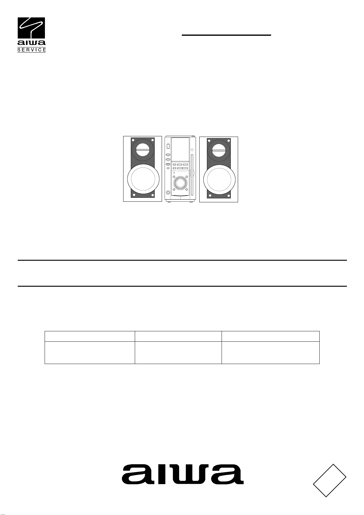
XR-MSK3
HRJ(S)
HRJ7(S)
SERVICE MANUAL
CONPACT DISC STEREO
SYSTEM
SYSTEM SPEAKER REMOTE CONTROL
XR-MSK3 SX-MS7 RC-AAT20
BASIC CD MECHANISM : TN-CCD1001-149M
S/M Code No. 09-00A-351-3N1
DATA
Page 2

TABLE OF CONTENTS
SPECIFICATIONS...........................................................................................................................................................................3
ACCESSORIES LIST ......................................................................................................................................................................3
PROTECTION OF EYES FROM LASER BEAM DURING SERVING ............................................................................................4
PRECAUTION TO REPLACE OPTICAL BLOCK............................................................................................................................4
DISASSEMBLY INSTRUCTIONS ............................................................................................................................................... 5, 6
ELECTRICAL MAIN PARTS LIST ........................................................................................................................................... 7 ~ 11
TRANSISTOR ILLUSTRATION..................................................................................................................................................... 11
SCHEMATIC DIAGRAM - 1 (MAIN - 1/2 SECTION) ..................................................................................................................... 12
SCHEMATIC DIAGRAM - 2 (MAIN - 2/2 SECTION) ..................................................................................................................... 13
SCHEMATIC DIAGRAM - 3 (FRONT SECTION)..........................................................................................................................16
SCHEMATIC DIAGRAM - 4 (VCD - 1/2 SECTION) ...................................................................................................................... 18
SCHEMATIC DIAGRAM - 5 (VCD - 2/2 SECTION) ...................................................................................................................... 19
SCHEMATIC DIAGRAM - 6 (CD SECTION) ................................................................................................................................. 21
SCHEMATIC DIAGRAM - 7 (TUNER SECTION)..........................................................................................................................23
SCHEMATIC DIAGRAM - 8 (PT SECTION).................................................................................................................................. 25
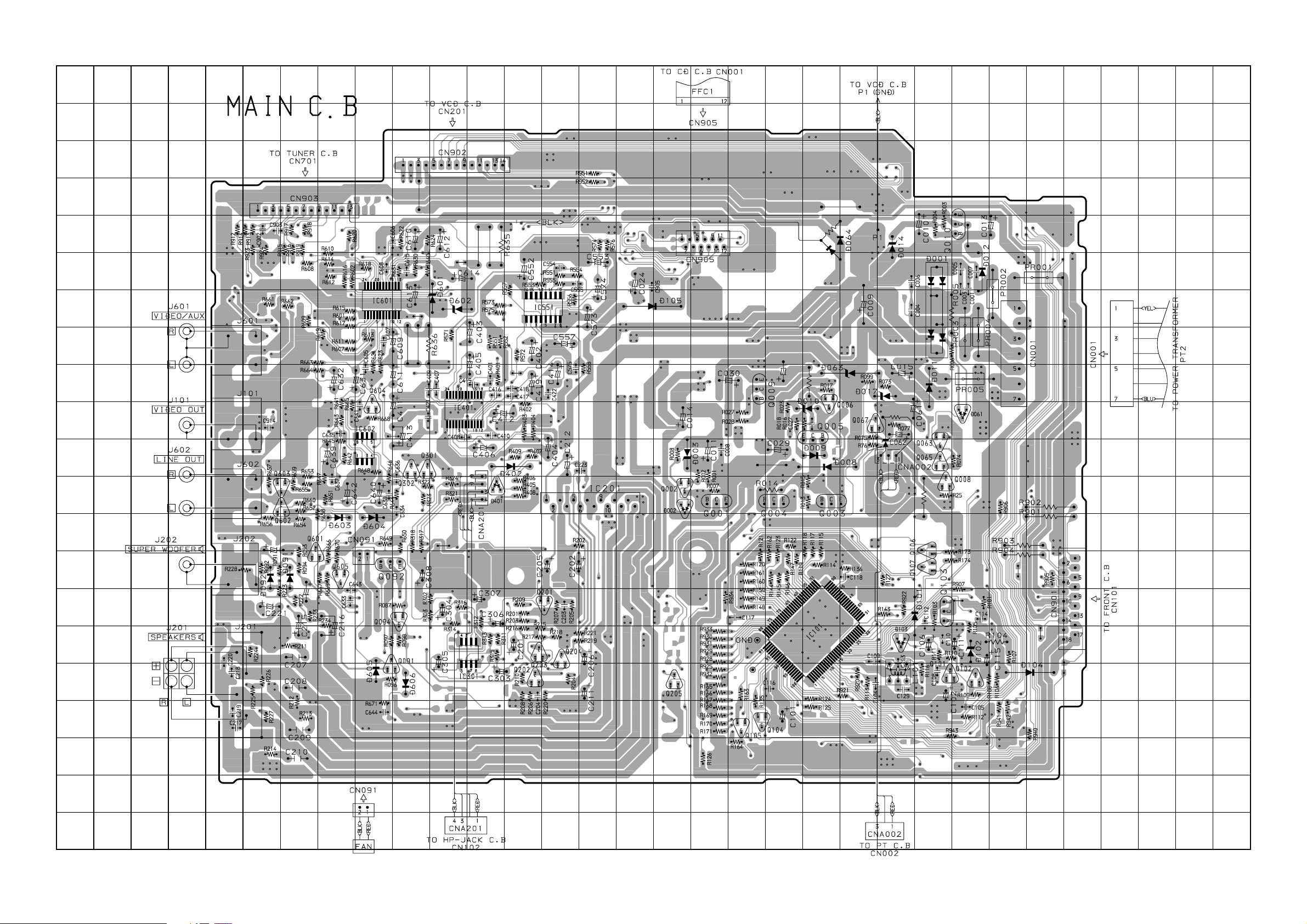
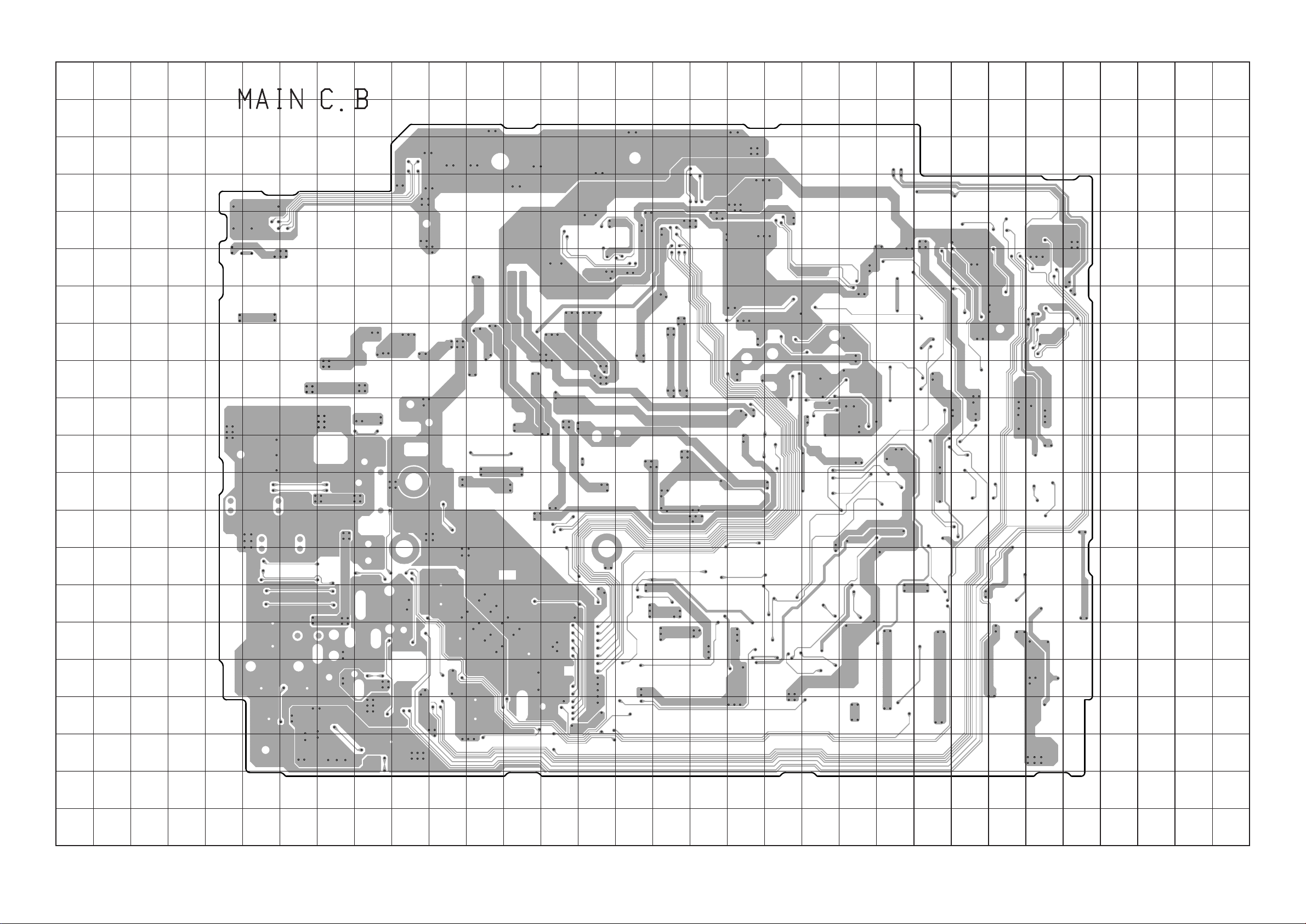
WIRING - 1 (MAIN - 1/2 C.B) ........................................................................................................................................................14
WIRING - 2 (MAIN - 2/2 C.B) ........................................................................................................................................................15
WIRING - 3 (FRONT, HP-JACK C.B) ............................................................................................................................................ 17
WIRING - 4 (VCD C.B)..................................................................................................................................................................20
WIRING - 5 (CD C.B) ....................................................................................................................................................................22
WIRING - 6 (TUNER C.B) ............................................................................................................................................................. 24
WIRING - 7 (PT C.B) .....................................................................................................................................................................25
IC BLOCK DIAGRAM........................................................................................................................................................23, 26, 27
IC DESCRIPTION .................................................................................................................................................................28 ~ 45
FL (9-ST-19GONK) GRID ASSIGNMENT/ANODE CONNECTION......................................................................................46 ~ 48
ADJUSTMENT (TUNER, MAIN SECTION)...................................................................................................................................49
MECHANICAL EXPLODED VIEW 1/1 ..........................................................................................................................................50
MECHANICAL MAIN PARTS LIST 1/1......................................................................................................................................... 51
CD MECHANISM EXPLODED VIEW 1/1 ..................................................................................................................................... 52
CD MECHANISM PARTS LIST 1/1 ............................................................................................................................................... 53
GENERAL SPEAKER DISASSEMBLY INSTRUCTIONS (FOR REFERENCE) ........................................................................... 54
SPEAKER PARTS LIST ................................................................................................................................................................55
-2-
Page 3
SPECIFICATIONS
• Design and specifications are subject to change without notice.
• The word “BBE” and the “BBE symbol” are trademarks of BBE
Sound, Inc.
• Under license from BBE Sound, Inc.
ACCESSORIES LIST
REF. NO PART NO. KANRI DESCRIPTION
1 8A-CG5-901-010 IB,H(EC)M
2 8A-CG5-951-010 RC UNIT,RC-AAT20
3 87-006-225-010 AM LOOP ANT NC2
4 87-043-115-010 ANT,FEEDER FM
5 87-050-103-010 CORD,PIN 1PY1.5M
!!
! 6 87-A91-017-010 PLUG,CONVERSION JT-0476
!!
NO.
-3-
Page 4
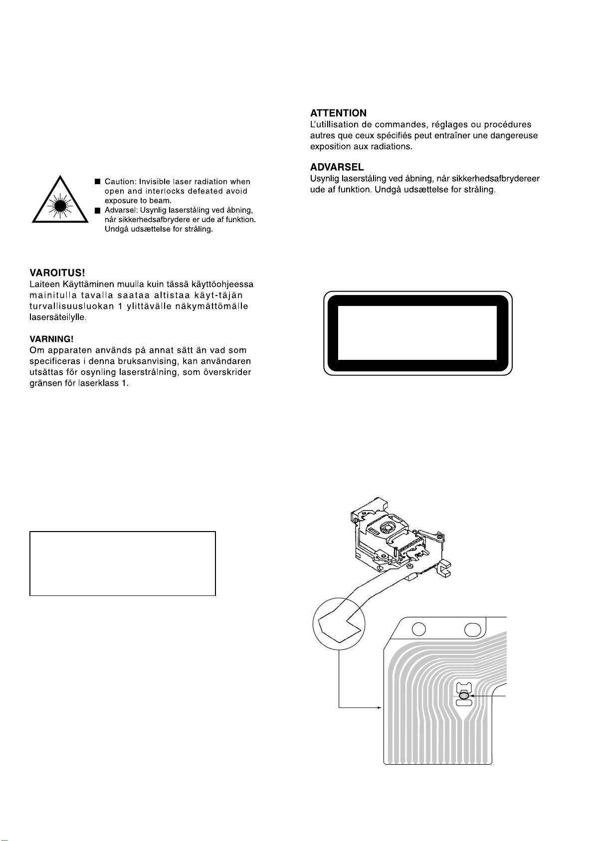
PROTECTION OF EYES FROM LASER BEAM DURING SERVICING
This set employs laser. Therefore, be sure to follow carefully
the instructions below when servicing.
WARNING!!
WHEN SERVICING, DO NOT APPROACH THE LASER
EXIT WITH THE EYE TOO CLOSELY. IN CASE IT IS
NECESSARY TO CONFIRM LASER BEAM EMISSION.
BE SURE TO OBSERVE FROM A DISTANCE OF MORE
THAN 30cm FROM THE SURFACE OF THEOBJECTIVE LENS ON THE OPTICAL PICK-UP BLOCK.
CAUTION
Use of controls or adjustments or performance of procedures other than those specified herin may result in
hazardous radiation exposure.
This Compact Disc player is classified as a CLASS 1
LASER product.
The CLASS 1 LASER PRODUCT label is located on the
rear exterior.
CLASS 1 LASER PRODUCT
KLASSE 1 LASER PRODUKT
LUOKAN 1 LASER LAITE
KLASS 1 LASER APPARAT
Precaution to replace Optical block
(VED0375-TN)
Body or clothes electrostatic potential could
ruin laser diode in the optical block. Be sure
ground body and workbench, and use care the
clothes do not touch the diode.
1) After the connection, remove solder shown in
right figure.
PICK-UP ASSY
VED0375-TN
SOLDER
-4-
Page 5
DISASSEMBLY INSTRAUCTIONS
1. CD BLOCK
1) Remove the PANEL, SIDE.
Remove the four screws indicated by the arrows
and remove the PANEL, SIDE (right and left).
2) Remove the CABI, TOP ASSY.
Remove the five screws indicated by the arrows
and remove the CABI, TOPASSY.
Screw
PANEL,SIDE
Screw
Screw
Screw
Screw
CABI,TOP ASSY
3) Remove the CABI, REAR.
Remove the nine screws indicated by the arrows and
remove the CABI, REAR.
Screw
Screw
Screw
CABI,REAR
Screw
-5-
Screw
Page 6
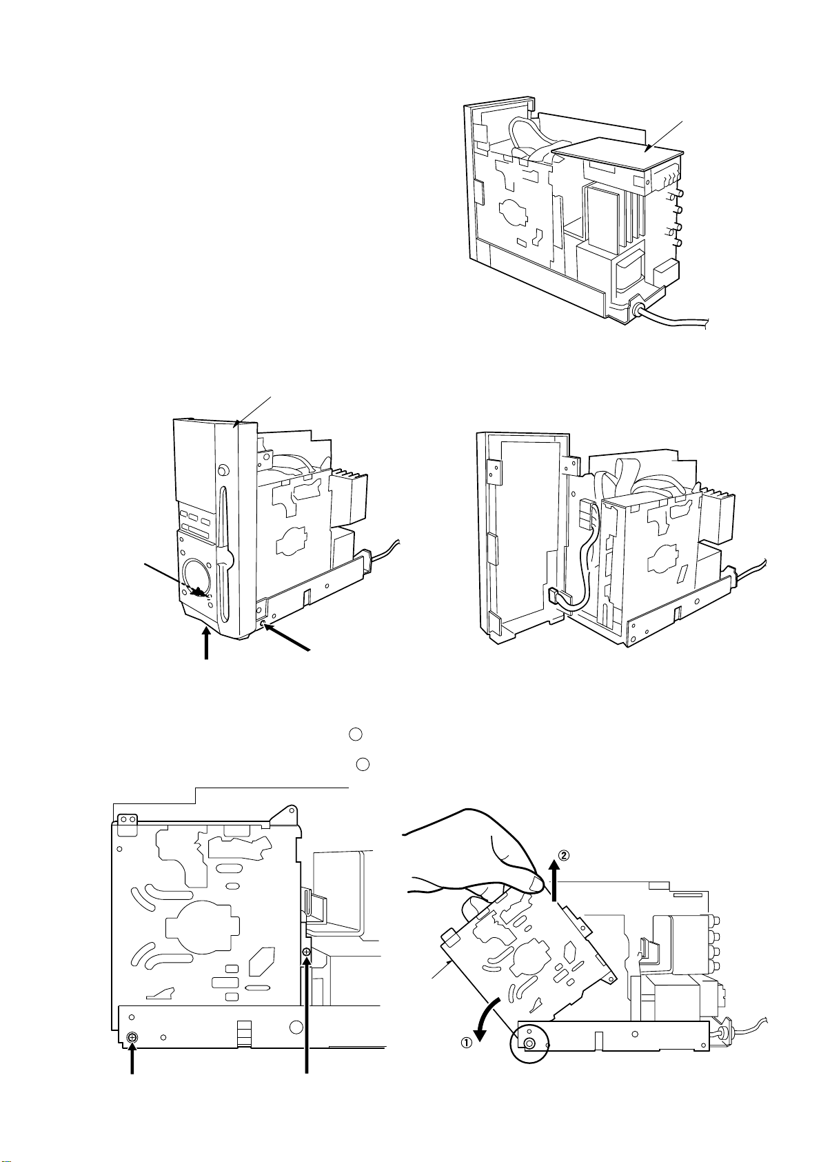
4) Remove the TUNER board.
Remove the TUNER board connected to the connector.
5) Remove the CABI, FR ASSY.
Remove the three screws indicated by the arrows and remove
the CABI, FR ASSY.
CABI,FR ASSY
TUNER board
Screw
Screw
6) Remove the CD MECHA.
(1) Remove the two screws indicated by the arrows.
(2) Lift up the CD MECHA in the direction of arrow 1 and
hook in the position indicated in circle.
(3) Remove the CD MECHA in the direction of arrow 2 .
Screw
Screw Screw
CD MECHA
Hook
-6-
Page 7

ELECTRICAL MAIN PARTS LIST
REF. NO PART NO. KANRI DESCRIPTION
IC
87-070-246-010 IC,GP1U271X
87-A20-909-010 IC,LA4663
87-017-915-080 IC,BU4094BCF
87-017-585-080 IC,NJM4580E
87-A21-022-040 C-IC,BA3880FS
87-A21-103-040 C-IC,MM1454XFBE
87-A21-111-040 C-IC,M62495FP
8A-CG5-602-010 C-IC,CXP84332-169Q
87-A21-777-040 C-IC,BA6289F
87-017-760-080 IC,M51943BML
87-017-853-040 IC,NJM2100V
87-A21-894-040 C-IC,UPC4742G2
87-A20-547-010 C-IC,CXA1992AR
8A-CG5-601-030 C-IC,LC876564V-5S40
87-A20-919-040 C-IC,BA5915FP
87-017-917-080 IC,BU4066BCF
87-A20-917-010 C-IC,CXD2540Q-1/2
8A-CG6-640-030 C-IC,UPD78016FGC-583
87-A20-602-040 C-IC,M5291FP
87-A20-925-040 C-IC,BA05FP
87-A20-905-040 C-IC,BA033FP
87-A20-920-010 C-IC,CL680-D1
87-A20-921-040 C-IC,SN74LVU04APW
87-A20-962-040 C-IC,MSM54V16258B/BSL
84-ZG1-695-040 C-IC,LH5V2RN1
87-A20-975-040 C-IC,SN74LV74APW
87-A20-974-040 C-IC,LC74781M-9017
87-A20-918-040 C-IC,SM5878AM
87-A21-419-040 C-IC,NJM14558MD-TE2
87-070-127-110 IC,LC72131 D
87-A20-913-010 IC,LA1837NL
TRANSISTOR
89-213-702-010 TR,2SB1370E(1.8W)
87-A30-076-080 C-TR,2SC3052F
87-026-610-080 TR,KTC3198GR
87-A30-075-080 C-TR,2SA1235F
87-A30-234-080 TR,CSC4115BC
89-418-580-080 TR,2SD1858 TV2
87-026-245-080 TR,DTC114ES
87-A30-198-080 TR,KTC3199GR
87-026-609-080 TR,KTA1266GR
87-A30-087-080 C-FET,2SK2158
87-A30-073-080 C-TR,RT1N 141C
87-A30-273-040 C-TR,DTC124EKA
87-A30-086-070 C-TR,CSD1306E
87-A30-072-080 C-TR,RT1P 144C
89-111-624-080 C-TR,2SA1162Y
87-026-237-080 CHIP-TR,DTC124XK
89-327-125-080 CHIP TR,2SC2712GR
87-026-350-040 CHIP-TR,DTC114TUA
87-026-231-080 CHIP-TRANSISTER,DTA124XK
87-026-211-080 C-TR,DTA144EK
87-026-210-080 CHIP-TR,DTC144EK
87-A30-117-010 TR,2SA1357
89-111-625-080 C-TR,2SA1162GR(0.15W)
87-026-297-080 C-TR,DTA144TK
87-026-580-080 C-TR,DTA123JK
87-026-470-080 C-TR,HN1C03FB(0.3W)
89-327-143-080 C-TR,2SC2714O
DIODE
87-020-465-080 DIODE,1SS133 (110MA)
87-A40-313-080 C-DIODE,MC 2840
87-A40-346-080 ZENER,MTZJ 8.2C
87-A40-345-080 ZENER,MTZJ10C
NO.
REF. NO PART NO. KANRI DESCRIPTION
87-070-274-080 DIODE,1N4003 SEM
87-A40-336-080 ZENER,MTZJ27D T-72
87-A40-270-080 C-DIODE,MC2838
87-A40-004-080 ZENER,MTZJ16A
87-070-136-080 ZENER,MTZJ5.1B
87-A40-509-080 ZENER,MTZJ6.8C
87-A40-269-080 C-DIODE,MC2836
87-A40-293-080 ZENER,DZ2.7M
87-017-654-060 DIODE,GBU6J
87-A40-874-040 C-ZENER,UDZS 5.6B
87-A40-335-080 ZENER,MTZJ11C
87-A40-341-080 ZENER,MTZJ 36 A
87-020-027-080 CHIP-DIODE 1SS184
87-017-024-040 C-DIODE,DA204K
87-A40-180-040 C-DIODE,SB07-015C
87-001-731-080 ZENER,HZS6C2L
87-017-149-080 ZENER,HZS6A2L
MAIN C.B
C1 87-012-369-080 C-CAP,S 0.047-50F
C3 87-012-368-080 C-CAP,S 0.1-50 F
C4 87-012-368-080 C-CAP,S 0.1-50 F
C5 87-012-368-080 C-CAP,S 0.1-50 F
C6 87-012-368-080 C-CAP,S 0.1-50 F
C7 87-012-369-080 C-CAP,S 0.047-50F
C8 87-012-368-080 C-CAP,S 0.1-50 F
C9 87-A12-033-090 CAP,E 6800-25 SMG30L
C10 87-010-409-080 CAP,E 220-50 SME
C11 87-010-553-080 CAP,E 47-16
C13 87-010-247-080 CAP, ELECT 100-50V
C14 87-010-235-080 CAP,E 470-16 SME
C15 87-010-387-080 CAP,E 470-25 SME
C24 87-016-251-080 CAP,E 220-16 M SMG
C27 87-012-140-080 CAP 470P
C29 87-010-247-080 CAP, ELECT 100-50V
C30 87-016-044-080 CAP,E 100-16 5L GAS
C31 87-010-235-080 CAP,E 470-16 SME
C61 87-010-260-080 CAP, ELECT 47-25V
C62 87-010-496-080 CAP,E 3.3-50 5L
C91 87-010-401-080 CAP, ELECT 1-50V
C92 87-010-260-080 CAP, ELECT 47-25V
C101 87-A11-242-040 CAP,E 220-10 M 5L SRM
C102 87-A11-242-040 CAP,E 220-10 M 5L SRM
C103 87-010-196-080 CHIP CAPACITOR,0.1-25
C104 87-010-993-080 CAP, CHIP 0.056
C105 87-010-196-080 CHIP CAPACITOR,0.1-25
C106 87-010-493-040 CAP,E 0.47-50 GAS
C108 87-010-157-080 C-CAP,S 18P-50 SL
C109 87-012-156-080 C-CAP,S 220P-50 CH
C110 87-010-196-080 CHIP CAPACITOR,0.1-25
C111 87-010-079-040 CAP,E 100-6.3 5L
C112 87-010-194-080 CAP, CHIP 0.047
C114 87-010-194-080 CAP, CHIP 0.047
C115 87-010-498-040 CAP,E 10-16 GAS
C116 87-010-196-080 CHIP CAPACITOR,0.1-25
C117 87-010-196-080 CHIP CAPACITOR,0.1-25
C118 87-010-196-080 CHIP CAPACITOR,0.1-25
C129 87-010-316-080 C-CAP,S 33P-50 CH
C201 87-010-491-040 CAP,E 0.22-50 GAS
C202 87-010-491-040 CAP,E 0.22-50 GAS
C203 87-010-178-080 CHIP CAP 1000P
C204 87-010-178-080 CHIP CAP 1000P
C205 87-010-492-040 CAP,E 0.33-50 GAS
C206 87-010-492-040 CAP,E 0.33-50 GAS
C211 87-010-560-040 CAP,E 10-50 GAS
C212 87-010-260-080 CAP, ELECT 47-25V
C215 87-010-405-080 CAP, ELECT 10-50V
C216 87-010-405-080 CAP, ELECT 10-50V
C217 87-012-368-080 C-CAP,S 0.1-50 F
NO.
-7-
Page 8

REF. NO PART NO. KANRI DESCRIPTION
NO.
C218 87-012-368-080 C-CAP,S 0.1-50 F
C219 87-012-368-080 C-CAP,S 0.1-50 F
C220 87-012-368-080 C-CAP,S 0.1-50 F
C221 87-010-405-080 CAP, ELECT 10-50V
C223 87-012-368-080 C-CAP,S 0.1-50 F
C303 87-016-044-040 CAP,E 100-16 GAS
C304 87-016-044-040 CAP,E 100-16 GAS
C305 87-010-494-040 CAP,E 1-50 GAS
C306 87-010-494-040 CAP,E 1-50 GAS
C307 87-010-553-040 CAP,E 47-16 GAS
C308 87-016-044-040 CAP,E 100-16 GAS
C401 87-010-196-080 CHIP CAPACITOR,0.1-25
C402 87-010-260-080 CAP, ELECT 47-25V
C403 87-010-404-080 CAP, ELECT 4.7-50V
C404 87-010-404-080 CAP, ELECT 4.7-50V
C405 87-010-404-080 CAP, ELECT 4.7-50V
C406 87-010-404-080 CAP, ELECT 4.7-50V
C407 87-010-188-080 CAP,CHIP 6800P
C408 87-010-188-080 CAP,CHIP 6800P
C409 87-012-140-080 CAP 470P
C410 87-012-140-080 CAP 470P
C411 87-010-404-080 CAP, ELECT 4.7-50V
C412 87-010-404-080 CAP, ELECT 4.7-50V
C413 87-010-404-080 CAP, ELECT 4.7-50V
C414 87-010-404-080 CAP, ELECT 4.7-50V
C415 87-010-197-080 CAP, CHIP 0.01 DM
C416 87-010-197-080 CAP, CHIP 0.01 DM
C417 87-010-956-080 CHIP-CAP,S 0.068-25B
C418 87-010-956-080 CHIP-CAP,S 0.068-25B
C419 87-010-260-080 CAP, ELECT 47-25V
C421 87-012-140-080 CAP 470P
C422 87-012-140-080 CAP 470P
C552 87-010-112-080 CAP, ELECT 100-16V
C553 87-010-260-080 CAP, ELECT 47-25V
C554 87-010-197-080 CAP, CHIP 0.01 DM
C555 87-010-197-080 CAP, CHIP 0.01 DM
C557 87-010-405-080 CAP, ELECT 10-50V
C573 87-010-405-080 CAP, ELECT 10-50V
C574 87-010-405-080 CAP, ELECT 10-50V
C575 87-010-322-080 C-CAP,S 100P-50 CH
C605 87-010-182-080 C-CAP,S 2200P-50 B
C606 87-010-182-080 C-CAP,S 2200P-50 B
C607 87-010-213-080 C-CAP,S 0.015-50 B
C608 87-010-213-080 C-CAP,S 0.015-50 B
C609 87-010-491-080 CAP,E 0.22-50 GAS
C610 87-010-491-080 CAP,E 0.22-50 GAS
C611 87-010-491-080 CAP,E 0.22-50 GAS
C612 87-010-491-080 CAP,E 0.22-50 GAS
C613 87-010-553-080 CAP,E 47-16
C614 87-010-553-080 CAP,E 47-16
C615 87-010-154-080 CAP CHIP 10P
C631 87-010-401-080 CAP, ELECT 1-50V
C632 87-010-401-080 CAP, ELECT 1-50V
C633 87-010-197-080 CAP, CHIP 0.01 DM
C634 87-010-197-080 CAP, CHIP 0.01 DM
C635 87-012-154-080 C-CAP,S 150P-50 CH
C636 87-012-154-080 C-CAP,S 150P-50 CH
C637 87-012-154-080 C-CAP,S 150P-50 CH
C638 87-012-154-080 C-CAP,S 150P-50 CH
C639 87-010-404-080 CAP, ELECT 4.7-50V
C640 87-010-404-080 CAP, ELECT 4.7-50V
C641 87-010-196-080 CHIP CAPACITOR,0.1-25
C642 87-010-381-080 CAP, ELECT 330-16V
C643 87-010-805-080 CAP, S 1-16
C644 87-010-196-080 CHIP CAPACITOR,0.1-25
C902 87-012-156-080 C-CAP,S 220P-50 CH
C903 87-010-322-080 C-CAP,S 100P-50 CH
C905 87-010-196-080 CHIP CAPACITOR,0.1-25
C914 87-010-196-080 CHIP CAPACITOR,0.1-25
CN1 87-A61-142-010 CONN,7P V THL-P07-A1
REF. NO PART NO. KANRI DESCRIPTION
CN91 87-A60-619-010 CONN,2P V 2MM JMT
CN901 87-A60-770-010 CONN,18P B TMC-D(X)
CN902 87-009-799-010 CONN,14P TKC-M X
CN903 87-099-570-010 CONN,13P TUC-P13P-B1
CN905 87-A60-901-010 CONN,12P V BLK FMN-BTRK
CNA2 88-805-030-820 CONN ASSY,3P 80
CNA201 88-805-043-020 CONN ASSY,4P 300
J101 87-099-208-010 JACK,PIN 1P YEL
J201 87-A60-238-010 TERMINAL,SP 4P (MSC)
J202 87-099-801-010 JACK,PIN 1P BLK
J601 87-A60-881-010 JACK,PIN 2P MSP 242V05 PBSN
J602 87-A60-881-010 JACK,PIN 2P MSP 242V05 PBSN
L101 87-A50-333-010 COIL,OSC 9.43MHZ
!!
!PR1 87-A90-393-080 PROTECTOR,0.5A 491SERISE 60V
!!
!!
!PR2 87-026-689-080 PROTECTOR,1A 60V 491
!!
!!
!PR3 87-A90-195-080 PROTECTOR 7A 60V 491
!!
!!
!PR4 87-A90-195-080 PROTECTOR 7A 60V 491
!!
!!
!PR5 87-026-689-080 PROTECTOR,1A 60V 491
!!
FRONT C.B
C102 87-010-415-040 CAP,E 10-50 5L
C103 87-012-157-080 C-CAP,S 330P-50 CH
C104 87-010-421-040 CAP,E 4.7-50 5L
C105 87-010-421-040 CAP,E 4.7-50 5L
C106 87-010-408-040 CAP,E 47-50 SME
C107 87-012-369-080 C-CAP,S 0.047-50F
C108 87-010-197-080 CAP, CHIP 0.01 DM
C109 87-010-197-080 CAP, CHIP 0.01 DM
C110 87-010-196-080 CHIP CAPACITOR,0.1-25
C111 87-012-368-080 C-CAP,S 0.1-50 F
C301 87-010-196-080 CHIP CAPACITOR,0.1-25
CN101 87-A60-778-010 CONN,18P B TMC-D(P)
FL101 8A-CL5-608-010 FL,9-ST-19GONK
LED101 87-A40-317-080 LED,SLR-342VCT31 RED
LED301 87-A40-786-080 LED,SMLS1BE16WTP4 BLU/UMB
LED302 87-A40-786-080 LED,SMLS1BE16WTP4 BLU/UMB
LED303 87-A40-786-080 LED,SMLS1BE16WTP4 BLU/UMB
R102 87-022-355-080 C-RES,S10K-1/10W F
R103 87-022-355-080 C-RES,S10K-1/10W F
S102 87-A91-743-010 SW,JOG 3-2-1RE01311 PCE2
S201 87-A90-095-080 SW,TACT EVQ11G04M
S202 87-A90-095-080 SW,TACT EVQ11G04M
S203 87-A90-095-080 SW,TACT EVQ11G04M
S204 87-A90-095-080 SW,TACT EVQ11G04M
S205 87-A90-095-080 SW,TACT EVQ11G04M
S206 87-A90-095-080 SW,TACT EVQ11G04M
S207 87-A90-095-080 SW,TACT EVQ11G04M
S208 87-A90-095-080 SW,TACT EVQ11G04M
S209 87-A90-095-080 SW,TACT EVQ11G04M
S210 87-A90-095-080 SW,TACT EVQ11G04M
S211 87-A90-095-080 SW,TACT EVQ11G04M
S212 87-A90-095-080 SW,TACT EVQ11G04M
S213 87-A90-095-080 SW,TACT EVQ11G04M
S214 87-A90-095-080 SW,TACT EVQ11G04M
S215 87-A90-095-080 SW,TACT EVQ11G04M
S216 87-A90-095-080 SW,TACT EVQ11G04M
HP-JACK C.B
CN102 87-A60-668-010 CONN,4P H 2MM JMT
J101 87-A60-420-010 JACK,3.5 ST (MSC)
VCD C.B
C101 87-012-278-080 C-CAP,U 2200P-50 B
C102 87-A12-319-080 C-CAP,U 0.1-25 K B
C103 87-A12-319-080 C-CAP,U 0.1-25 K B
C104 87-A12-319-080 C-CAP,U 0.1-25 K B
C105 87-010-404-040 CAP,E 4.7-50 SME
NO.
-8-
Page 9

REF. NO PART NO. KANRI DESCRIPTION
NO.
C106 87-010-788-080 C-CAP,U 0.033-25 Z F
C107 87-012-286-080 CAP, U 0.01-25
C108 87-010-401-040 CAP,E 1-50 SME
C109 87-010-382-040 CAP,E 22-25 SME
C110 87-010-785-080 C-CAP,U0.015-25BK
C111 87-010-263-040 CAP,E 100-10
C112 87-012-286-080 CAP, U 0.01-25
C113 87-010-788-080 C-CAP,U 0.033-25 Z F
C114 87-010-788-080 C-CAP,U 0.033-25 Z F
C115 87-010-788-080 C-CAP,U 0.033-25 Z F
C116 87-012-269-080 C-CAP,U 390P-50 B
C117 87-012-197-080 C-CAP,U 150P-50 CH
C118 87-010-401-040 CAP,E 1-50
C119 87-012-174-080 C-CAP,U 12P-50 CH
C120 87-010-194-080 C.CAP,S 0.047-25F
C121 87-010-194-080 C.CAP,S 0.047-25F
C122 87-010-805-080 C-CAP,S 1-16 Z F
C123 87-A12-319-080 C-CAP,U 0.1-25 K B
C125 87-010-198-080 CAP, S 0.022-25
C126 87-A12-319-080 C-CAP,U 0.1-25 K B
C127 87-010-263-040 CAP,E 100-10
C128 87-012-166-080 C-CAP,U 4P-50 C CH
C130 87-010-263-040 CAP,E 100-10
C131 87-010-263-040 CAP,E 100-10
C132 87-010-178-080 CHIP CAP,S 1000P-50B
C133 87-010-263-040 CAP,E 100-10
C134 87-010-196-080 CHIP CAPACITOR,0.1-25
C135 87-010-196-080 CHIP CAPACITOR,0.1-25
C136 87-010-196-080 CHIP CAPACITOR,0.1-25
C137 87-010-759-080 C-CAP,U, 0.1-25F
C138 87-012-280-080 CAP, U 3300P-50
C139 87-010-197-080 CAP, CHIP 0.01 DM
C140 87-010-112-040 CAP,E 100-16
C141 87-010-759-080 C-CAP,U, 0.1-25F
C142 87-010-322-080 C-CAP,S 100P-50 CH
C143 87-A12-319-080 C-CAP,U 0.1-25 K B
C151 87-010-263-040 CAP,E 100-10
C152 87-012-286-080 CAP, U 0.01-25
C153 87-A10-893-040 CAP,E 220-10 M PW
C154 87-012-286-080 CAP, U 0.01-25
C155 87-010-184-080 CAP, S 3300P-50
C156 87-010-194-080 C.CAP,S 0.047-25F
C157 87-010-194-080 C.CAP,S 0.047-25F
C158 87-012-199-080 CAP 220P
C159 87-012-358-080 C-CAP,S 0.47-10
C161 87-012-278-080 C-CAP,U 2200P-50 B
C162 87-012-274-080 CHIP CAP,U 1000P-50B
C201 87-A12-319-080 C-CAP,U 0.1-25 K B
C206 87-012-195-080 C-CAP,U 100P-50CH
C207 87-012-195-080 C-CAP,U 100P-50CH
C208 87-012-195-080 C-CAP,U 100P-50CH
C209 87-012-195-080 C-CAP,U 100P-50CH
C210 87-016-669-080 C-CAP,S 0.1-25 K B
C211 87-010-263-040 CAP,E 100-10
C213 87-012-286-080 CAP, U 0.01-25
C214 87-010-759-080 C-CAP,U, 0.1-25F
C301 87-016-251-040 CAP,E 220-16 SMG
C302 87-A11-547-080 C-CAP,S 470P-50
C303 87-010-178-080 C-CAP,S 1000P-50B
C304 87-010-384-040 CAP,E 100-25 SME
C305 87-010-383-080 CAP,E 33-25
C306 87-010-112-040 CAP,E 100-16
C307 87-010-196-080 CHIP CAPACITOR,0.1-25
C308 87-010-263-040 CAP,E 100-10
C309 87-010-196-080 CHIP CAPACITOR,0.1-25
C310 87-010-263-040 CAP,E 100-10
C311 87-010-196-080 CHIP CAPACITOR,0.1-25
C312 87-010-178-080 C-CAP,S 1000P-50B
C320 87-010-196-080 CHIP CAPACITOR,0.1-25
C501 87-010-197-080 CAP, CHIP 0.01 DM
REF. NO PART NO. KANRI DESCRIPTION
NO.
C502 87-010-197-080 CAP, CHIP 0.01 DM
C503 87-012-286-080 CAP, U 0.01-25
C504 87-012-172-080 CAPACITOR CHIP U 10P CH
C505 87-012-172-080 CAPACITOR CHIP U 10P CH
C506 87-012-286-080 CAP, U 0.01-25
C508 87-010-263-040 CAP,E 100-10
C509 87-016-669-080 C-CAP,S 0.1-25 K B
C510 87-010-263-040 CAP,E 100-10
C511 87-010-196-080 CHIP CAPACITOR,0.1-25
C512 87-012-286-080 CAP, U 0.01-25
C513 87-012-286-080 CAP, U 0.01-25
C514 87-012-286-080 CAP, U 0.01-25
C518 87-010-322-080 C-CAP,S 100P-50 CH
C519 87-010-171-080 C-CAP,S 270P-50 SL
C520 87-010-172-080 C-CAP,S 330P-50 SL
C521 87-012-197-080 C-CAP,U 150P-50 CH
C522 87-010-371-080 CAP, ELECT 470-6.3V
C523 87-012-286-080 CAP, U 0.01-25
C524 87-012-286-080 CAP, U 0.01-25
C525 87-012-286-080 CAP, U 0.01-25
C526 87-012-286-080 CAP, U 0.01-25
C527 87-012-286-080 CAP, U 0.01-25
C528 87-012-286-080 CAP, U 0.01-25
C529 87-012-286-080 CAP, U 0.01-25
C530 87-012-286-080 CAP, U 0.01-25
C531 87-012-286-080 CAP, U 0.01-25
C532 87-010-374-040 CAP,E 47-10
C533 87-010-197-080 CAP, CHIP 0.01 DM
C534 87-010-263-040 CAP,E 100-10
C535 87-010-197-080 CAP, CHIP 0.01 DM
C536 87-015-676-040 CAP,E 47-6.3
C537 87-010-197-080 CAP, CHIP 0.01 DM
C538 87-010-759-080 C-CAP,U, 0.1-25F
C539 87-010-759-080 C-CAP,U, 0.1-25F
C540 87-015-676-040 CAP,E 47-6.3
C541 87-010-197-080 CAP, CHIP 0.01 DM
C542 87-012-188-080 C-CAP,U 47P-50 CH
C544 87-010-197-080 CAP, CHIP 0.01 DM
C546 87-012-286-080 CAP, U 0.01-25
C549 87-010-401-080 CAP,E 1-50
C550 87-010-759-080 C-CAP,U, 0.1-25F
C551 87-012-153-080 C-CAP,S 120P-50 CH
C552 87-012-358-080 C-CAP,S 0.47-10
C554 87-012-286-080 CAP, U 0.01-25
C556 87-010-197-080 CAP, CHIP 0.01 DM
C557 87-012-182-080 C-CAP,U 27P-50 J CH
C558 87-012-182-080 C-CAP,U 27P-50 J CH
C560 87-012-286-080 CAP, U 0.01-25
C601 87-012-286-080 CAP, U 0.01-25
C602 87-012-286-080 CAP, U 0.01-25
C603 87-010-112-040 CAP,E 100-16
C604 87-010-759-080 C-CAP,U 0.1-25F
C605 87-012-286-080 CAP, U 0.01-25
C606 87-010-197-080 CAP, CHIP 0.01 DM
C607 87-010-313-080 C-CAP,S 18P-50 CH
C608 87-010-313-080 C-CAP,S 18P-50 CH
C609 87-010-178-080 C-CAP,S 1000P-50B
C610 87-010-178-080 C-CAP,S 1000P-50B
C611 87-010-178-080 C-CAP,S 1000P-50B
C612 87-010-178-080 C-CAP,S 1000P-50B
C613 87-010-403-040 CAP,E 3.3-50 SME
C614 87-010-403-040 CAP,E 3.3-50 SME
C615 87-010-318-080 C-CAP,S 47P-50 CH
C616 87-010-318-080 C-CAP,S 47P-50 CH
CN101 87-A60-424-010 CONN,16P V TOC-B
CN102 87-A60-899-010 CONN,6P V BLK FMN-BTRK
CN201 87-099-545-010 CONN,14P TKC-M14P-B1
L101 87-005-196-080 COIL,10UH
L301 87-A50-095-010 COIL,68UH RCR875D
L302 87-005-426-080 COIL,3.3UH K FLR50
-9-
Page 10

REF. NO PART NO. KANRI DESCRIPTION
L502 87-005-204-080 COIL,47UH
L503 87-005-189-080 COIL 2.7UH
L504 87-005-187-080 COIL,1.8UH
L505 87-005-204-080 COIL,47UH
L506 87-005-204-080 COIL,47UH
L507 87-005-204-080 COIL,47UH
L508 87-005-817-080 C-COIL, 33UH J FLC32
R131 87-022-353-080 C-RES,6.8K 1/10WF
R132 87-022-353-080 C-RES,6.8K 1/10WF
R134 87-022-360-080 C-RES,S 39K-1/10W F
R135 87-022-360-080 C-RES,S 39K-1/10W F
R172 87-022-359-080 C-RES,S 22K-1/10W F
R173 87-022-359-080 C-RES,S 22K-1/10W F
R174 87-022-365-080 C-RES,100K-1/10WF
R175 87-022-365-080 C-RES,100K-1/10WF
R507 87-022-222-080 C-RES,U 2K-1/16W F
S201 87-A90-162-010 SW,SL 1-1-3 SSSU
X201 87-A70-124-080 VIB,CER 8.0MHZ
X501 87-A70-125-080 VIB,XTAL 27MHZ 50PPM
X601 87-030-270-080 VIB,XTAL 16.9344MHZ
CD C.B
C2 87-A11-156-080 C-CAP,E 22-25 SEH
C3 87-010-831-080 C-CAP,U,0.1-16F
C4 87-010-831-080 C-CAP,U,0.1-16F
C5 87-010-831-080 C-CAP,U,0.1-16F
C6 87-010-831-080 C-CAP,U,0.1-16F
C7 87-010-831-080 C-CAP,U,0.1-16F
C8 87-A11-156-080 C-CAP,E 22-25 SEH
C9 87-012-188-080 C-CAP,U 47P-50 CH
C10 87-012-188-080 C-CAP,U 47P-50 CH
C11 87-010-831-080 C-CAP,U,0.1-16F
C12 87-010-831-080 C-CAP,U,0.1-16F
C13 87-012-164-080 C-CAP,U 2P-50 C CH
C14 87-010-831-080 C-CAP,U,0.1-16F
C15 87-012-164-080 C-CAP,U 2P-50 C CH
C16 87-010-831-080 C-CAP,U,0.1-16F
C27 87-012-286-080 CAP, U 0.01-25
CN1 87-099-073-080 C-CONN,12P H 52207
CN2 87-A61-512-080 C-CONN,6P V FMN-BMTTR-TB
CN3 87-A61-478-080 C-CONN,6P H WHT ZR-SM3A-TF
CN4 87-009-214-080 CONN,16P 52207-1690
CN5 87-009-214-080 CONN,16P 52207-1690
CN6 87-A61-477-080 C-CONN,5P H WHT ZR-SM3A-TF
CN7 87-099-440-080 C-CONN,2P ZR-SM3 WHT
FFC1 8A-CG5-630-010 CABLE,FFC 12P-1.0-21
FFC2 8A-CG5-632-010 CABLE,FFC 6P-1.0-15
FFC4 8A-CG5-631-010 CABLE,FFC 16P-1.0-13
L3 87-A50-623-080 C-COIL,BK2125HS102
X1 87-A70-251-080 C-VIB,CER 10.00MHZ CSTCC
SW C.B
SW1 S6-418-040-030 DET SW ESE22 MH3
SW2 S6-418-040-020 DET SW ESE22 MH1
SW3 S6-418-040-020 DET SW ESE22 MH1
SW4 S6-418-040-030 DET SW ESE22 MH3
PT C.B
!!
!C1 87-A10-479-080 CAP,CER 2200P-250 M E KH
!!
C14 87-010-388-080 CAP ELECT 1000-25V SME
C106 87-010-496-080 CAP,E 3.3-50 5L
CN1 87-A60-851-010 CONN,9P V VH
CN2 87-A60-620-010 CONN,3P V 2MM JMT
!!
!PT1 8Z-NF8-663-010 PT,SUB ZNF-8(H)
!!
!!
!RY1 87-A91-281-010 RELAY,AC DC12V OSA-SS-212DM5
!!
!!
!S1 87-A90-234-010 SW,SL 1-2-2 SW2201
!!
!!
!T1 87-A60-317-010 TERMINAL, 1P MSC
!!
!!
!T2 87-A60-317-010 TERMINAL, 1P MSC
!!
NO.
REF. NO PART NO. KANRI DESCRIPTION
NO.
TUNER C.B
00000000000000 TUNER C.B
C0701 87-010-381-080 CAP,E 330-16 M SME
C0702 87-010-404-080 CAP,E 4.7-50 M 11L SME
C0703 87-012-286-080 C-CAP,U 0.01-25 K B
C0704 87-012-286-080 C-CAP,U 0.01-25 K B
C0705 87-A10-592-080 C-CAP,S 0.015-50 J B
C0706 87-A10-592-080 C-CAP,S 0.015-50 J B
C0709 87-012-195-080 C-CAP,U 100P-50 J CH
C0711 87-010-260-080 CAP,E 47-25 M 11L SME
C0712 87-010-831-080 C-CAP,U 0.1-16 Z F
C0714 87-012-286-080 C-CAP,U 0.01-25 K B
C0717 87-012-286-080 C-CAP,U 0.01-25 K B
C0719 87-012-286-080 C-CAP,U 0.01-25 K B
C0720 87-012-195-080 C-CAP,U 100P-50 J CH
C0721 87-012-176-080 C-CAP,U 15P-50 J CH
C0722 87-012-176-080 C-CAP,U 15P-50 J CH
C0723 87-012-274-080 C-CAP,U 1000P-50 K B
C0725 87-012-274-080 C-CAP,U 1000P-50 K B
C0727 87-010-196-080 C-CAP,S 0.1-25 Z F C2012
C0728 87-010-248-080 CAP,E 220-10 M 11L SME
C0729 87-012-274-080 C-CAP,U 1000P-50 K B
C0731 87-012-286-080 C-CAP,U 0.01-25 K B
C0733 87-010-987-080 C-CAP,S 1500P-50 J CH
C0734 87-010-987-080 C-CAP,S 1500P-50 J CH
C0735 87-010-987-080 C-CAP,S 1500P-50 J CH
C0736 87-010-987-080 C-CAP,S 1500P-50 J CH
C0737 87-A10-592-080 C-CAP,S 0.015-50 J B
C0738 87-A10-592-080 C-CAP,S 0.015-50 J B
C0751 87-010-220-080 C-CAP,S 0.018-25 K B
C0752 87-010-220-080 C-CAP,S 0.018-25 K B
C0756 87-012-286-080 C-CAP,U 0.01-25 K B
C0757 87-012-188-080 C-CAP,U 47P-50 J CH
C0758 87-012-167-080 C-CAP,U 5P-50 C CH
C0763 87-010-829-080 C-CAP,U 0.047-16 Z F
C0764 87-012-337-080 C-CAP,U 56P-50 J CH GRM
C0765 87-012-286-080 C-CAP,U 0.01-25 K B
C0768 87-012-286-080 C-CAP,U 0.01-25 K B
C0769 87-010-260-080 CAP,E 47-25 M 11L SME
C0770 87-010-829-080 C-CAP,U 0.047-16 Z F
C0771 87-010-383-080 CAP,E 33-25 M 11L SME
C0772 87-010-829-080 C-CAP,U 0.047-16 Z F
C0773 87-010-196-080 C-CAP,S 0.1-25 Z F C2012
C0774 87-010-263-080 CAP,E 100-10 M 11L SME
C0775 87-010-404-080 CAP,E 4.7-50 M 11L SME
C0776 87-012-286-080 C-CAP,U 0.01-25 K B
C0777 87-010-400-080 CAP,E 0.47-50 M 11L SME
C0778 87-010-401-080 CAP,E 1-50 M 11L SME
C0779 87-010-401-080 CAP,E 1-50 M 11L SME
C0780 87-010-196-080 C-CAP,S 0.1-25 Z F C2012
C0781 87-010-405-080 CAP,E 10-50 M 11L SME
C0782 87-010-405-080 CAP,E 10-50 M 11L SME
C0783 87-012-286-080 C-CAP,U 0.01-25 K B
C0784 87-012-286-080 C-CAP,U 0.01-25 K B
C0785 87-010-401-080 CAP,E 1-50 M 11L SME
C0786 87-010-401-080 CAP,E 1-50 M 11L SME
C0789 87-012-275-080 C-CAP,U 1200P-50 K B GRM
C0790 87-012-275-080 C-CAP,U 1200P-50 K B GRM
C0791 87-010-405-080 CAP,E 10-50 M 11L SME
C0793 87-012-273-080 C-CAP,U 820P-50 K B
C0794 87-010-406-080 CAP,E 22-50 M 11L SME
C0795 87-010-596-080 C-CAP,S 0.047-16 K R C2012
C0796 87-010-403-080 CAP,E 3.3-50 M 11L SME
C0799 87-010-829-080 C-CAP,U 0.047-16 Z F
C0812 87-012-286-080 C-CAP,U 0.01-25 K B
C0820 87-010-260-080 CAP,E 47-25 M 11L SME
C0821 87-012-286-080 C-CAP,U 0.01-25 K B
C0822 87-012-286-080 C-CAP,U 0.01-25 K B
C0823 87-012-286-080 C-CAP,U 0.01-25 K B
-10-
Page 11
REF. NO PART NO. KANRI DESCRIPTION
NO.
C0828 87-010-196-080 C-CAP,S 0.1-25 Z F C2012
C0829 87-010-196-080 C-CAP,S 0.1-25 Z F C2012
C0959 87-010-196-080 C-CAP,S 0.1-25 Z F C2012
C0960 87-010-196-080 C-CAP,S 0.1-25 Z F C2012
C0961 87-012-170-080 C-CAP,U 8P-50 D CH
C0963 87-010-196-080 C-CAP,S 0.1-25 Z F C2012
CF0801 87-008-261-010 FLTR,CF SFE10.7MA5
CF0802 87-008-261-010 FLTR,CF SFE10.7MA5
CN0701 87-A60-700-010 CONN,13P H GRY TUC-P13X-C1
FFE0801 A8-8ZA-194-030 8ZA-1 FEMUNM
REF. NO PART NO. KANRI DESCRIPTION
J0801 87-A60-702-010 TERMINAL,ANT 4P CJ-9036
L0771 87-A50-266-010 COIL,FM DET-2N(TOK)
L0772 87-A91-110-010 FLTR,PCFJZH-450 (TOK)
L0981 8Z-ZA1-667-010 COIL,AM PACK 4F(TOK)
X0721 87-A70-061-010 VIB,XTAL 4.500MHZ CSA-309
• Regarding connectors, they are not stocked as they are not the initial order items.
The connectors are available after they are supplied from connector manufacturers upon the order is received.
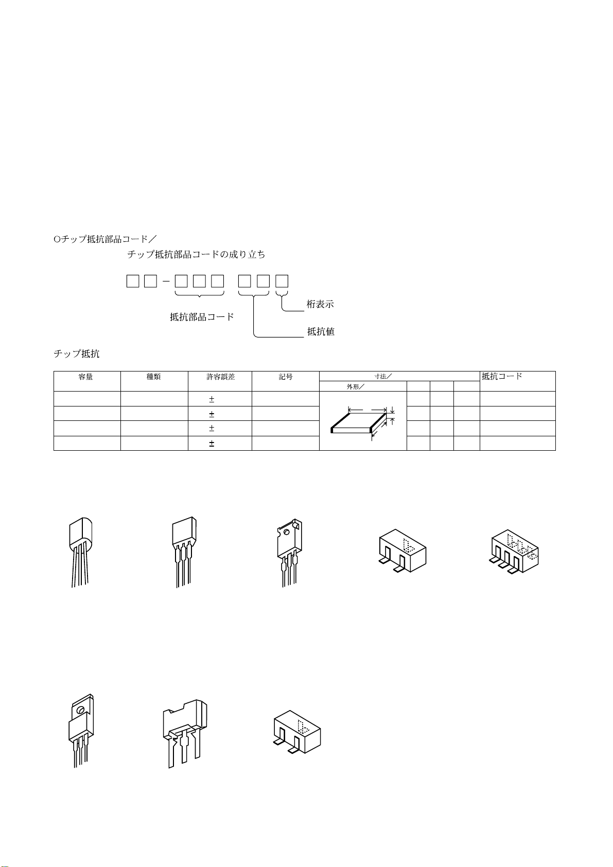
CHIP RESISTOR PART CODE
Chip Resistor Part Coding
88
NO.
Resistor Code
Chip resistor
Wattage Type Tolerance
1/16W 1005 5% CJ
1/16W
1/10W
1/8W
1608
2125
3216
TRANSISTOR ILLUSTRATION
E C B
CSC4115
KTA1266
KTC3198
B C E
2SB1370
E C B
DTC114ES
KTC3199
E C B
2SD1858
A
5%
5%
5%
Symbol
CJ
CJ
CJ
E C B
2SA1357
G
S
2SK2158
Figure
Value of resistor
Form
L
D
Dimensions (mm)
t
W
B
E
2SA1162
2SA1235
2SC2712
2SC2714
2SC3052
CSD1306
DTA123JK
DTA124XK
DTA144EK
DTA144TK
DTC114TUA
DTC124EKA
DTC124XK
DTC144EK
RT1N141C
RT1P144C
0.55
Resistor Code
108
118
128
C1
E1
B1
C2
HN1C03
LW t
1.0 0.5 0.35 104
1.6 0.8 0.45
2 1.25 0.45
3.2
1.6
C
B2
: A
: A
E2
-11-
Page 12
SCHEMATIC DIAGRAM - 1 (MAIN -1/2 SECTION)
2.7V
10V
10V
0V
4V
4V
11V
11V
0V
44V
27.9V
27V
8.5V
11V
11V
11V
8.3V
7.7V
0V-0.88V
0.6V-0.4V
1.2V-0V
20V
20V
-7V
19V
11V
11V
0.9V
0.5V
10V
11V
11V
11V
11V
11V
0.01V
3.7V
0.01V
0.6V
0.02V
0.6V
20V
20V
11V
-12-
Page 13
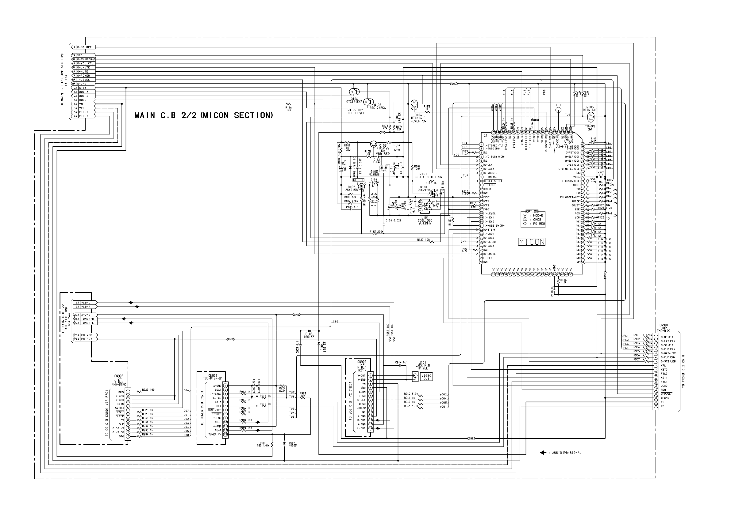
SCHEMATIC DIAGRAM - 2 (MAIN -2/2 SECTION)
5V-0V
0V-5V
5V-0V
0V-5V
10V 6V
6V
0V
5V
5V
AT CD: 5V
W/O CD: 0V
5V
5V
IC101 LC876564V-5S40
5V
AT CD: 5V
W/O CD: 0V
5V
5V
-13-
5.4V
11V
Page 14
WIRING - 1 (MAIN C.B 1/2)
181920212223242526272829303132
17 16151413121110987654321
A
B
C
D
C091
R908
D902
E
F
G
H
C031
R019
R010
I
J
D013
13
14
R024
K
L
M
C092
-14-
TP1
N
O
P
Q
R
S
T
U
Page 15
WIRING - 2 (MAIN C.B)
A
B
C
D
E
F
G
H
151413121110987654321
16 17 18 19 20 21 22 23 24 25 26 27 28 29 30 31 32
I
J
K
L
M
N
O
P
Q
R
S
T
U
-15-
Page 16
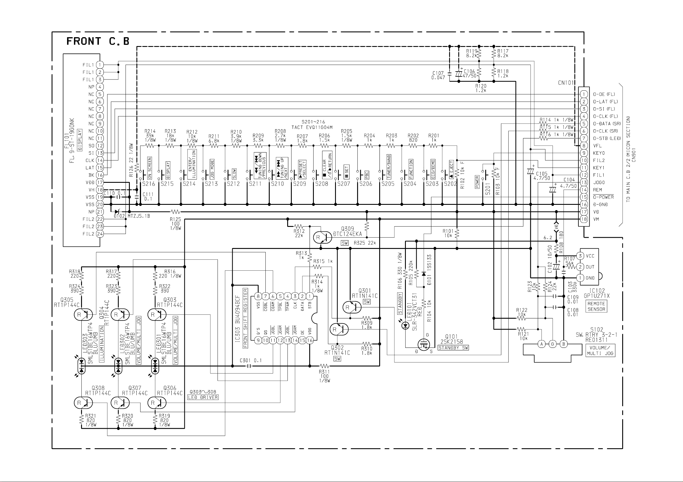
SCHEMATIC DIAGRAM - 3 (FRONT SECTION)
0V-11V
0V-11V
0V-11V
0V-11V
0V-11V
0V-11V
0V-11V
0V-11V
0V-11V
11V
0V-11V
0V-5V
0V-5V
11V
0V-11V 0V-11V 0V-11V
-16-
Page 17
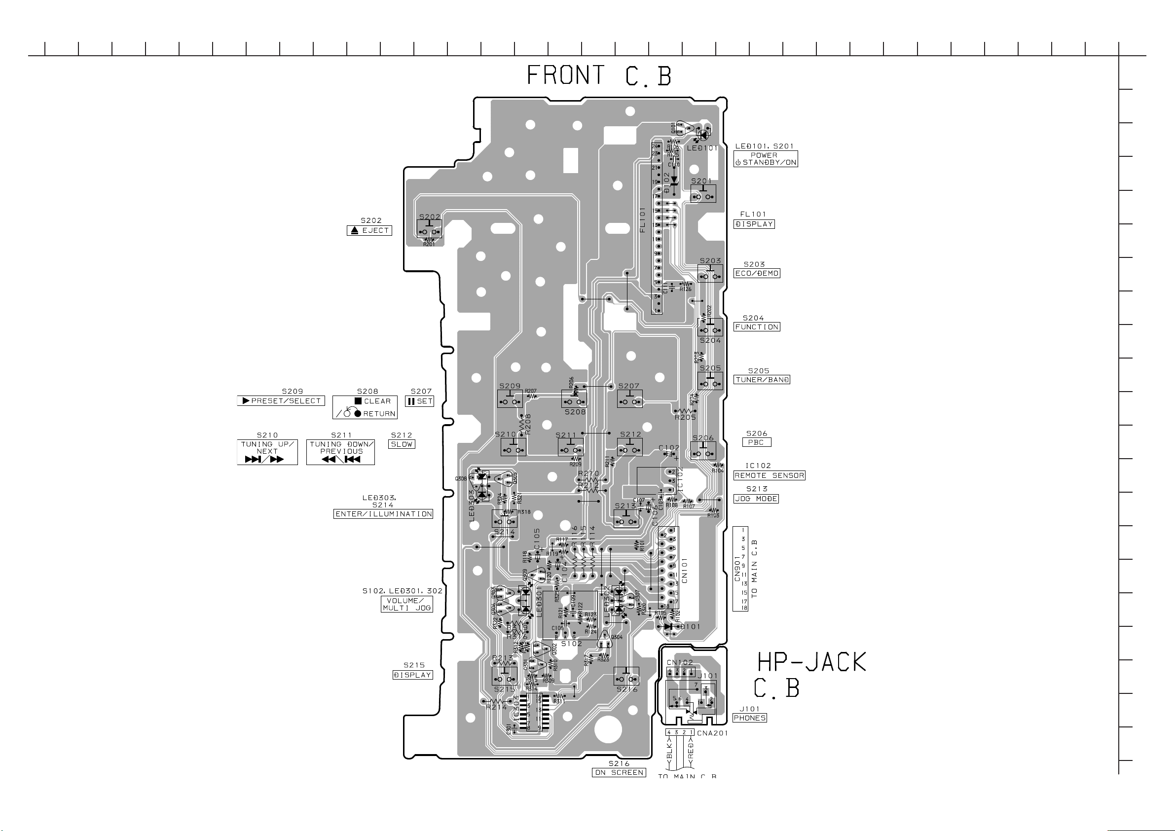
WIRING - 3 (FRONT, HP-JACK C.B)
101112131415161718192021222324
1234567892526272829303132
A
B
C
D
E
F
G
H
I
J
K
L
M
N
O
P
Q
-17-
R
S
T
U
Page 18

SCHEMATIC DIAGRAM - 4 (VCD-1/2 SECTION)
5V5V
2.47V
4.8V
4.6V
4.8V
4.6V
5V
5V
2.47V
2.46V
2.5V
2.46V
2.47V
2.5V
2.47V
5.7V
11V
7.6V
11V
7.6V
11V
11V
11V
0V
2.47V
0V
2.47V
2.6V
2.6V
2.46V
5.7V
2.47V
2.47V
2.47V
2.5V
2.5V
5.7V
11V
5V
5V
IN
GND
OUT
5V5.7V
IN
GND
OUT
3.3V
5.7V
5V
5V
5V
-18-
0V
5.3V
Page 19

SCHEMATIC DIAGRAM - 5 (VCD-2/2 SECTION)
4.7V
4.7V
-9017
4.8V
4.7V
4.7V
0V
4V
5V
5V
5V
5V
5V
5V
3V
5V
3V
3V
3V
3V 3V
5V
3V
3V
3V
3.2V
3.2V
3.2V
4.7V
3.2V
3.2V
3.4V
3V
3V
-19-
Page 20

WIRING - 4 (VCD C.B)
FFC4
FFC2
CN902
TO MAIN C.B
15
20
24
13
15
17
19
21
23
24
15
21
22
25
28 1
X201
2
A
A
B
B
876543211345678
9 10111213141516910111213141516
S201
4849
50
60
55
5
4
3
7
1
8
1
2
3
1
2
3
1213
10
5
1
12
11
9
7
5
3
1
14
10
8
7
5
64
1
5
10
8
10
14
8
10
14
1
7
45
40
35
25
20
161517
7
132
5
3
1
5
7
9
7
11
5
13
1
15
16
1415
13
20
25
26
27
30
35
40
39
14
12
3
5
10
8
C
C
33
32
30
31
29
27
25
23
21
19
17
5
10
1
52
45
50
D
D
E
E
F
F
G
G
H
H
I
I
J
J
K
K
L
L
M
M
N
N
O
O
P
P
Q
Q
R
R
S
S
T
T
32
1
23
25
30
32
35
40
1
5
10
15
20
25
30
32
128
22
20
15
13
10
5
144
110115120125
40
33
35
45 505560
97
100105
96
90
85
80
75
70
65
64
65
70
75
80
1 5 10 15
414550556064
40
35
30
20
25
24
U
-20-
U
Page 21

SCHEMATIC DIAGRAM - 6 (CD SECTION)
8.5V
8.5V
5.3V
5.3V
5.3V
5.3V
5.3V
5.3V
5.3V
5.3V
5.3V
5.3V
5.3V
5.3V
5.3V
5.3V
5.3V
5.3V
5.3V
5.3V
5.3V
5.3V
8.5V
5.3V
2.5V
2.5V
4.8V
2.5V
2.5V
2.5V
2.5V
2.5V
-21-
2.5V
2.5V
2.5V
2.5V
2.5V
4.8V
2.5V
UP
Page 22

WIRING - 5 (CD C.B)
-22-
Page 23

SCHEMATIC DIAGRAM - 7 (TUNER SECTION)
FEMUNM
7.5V
5.5V
10V
10
10V
4F
4F
4F
IC BLOCK DIAGRAM - 1
IC, LC72131D IC, LA1837NL
-23-
Page 24

WIRING - 6 (TUNER C.B)
101112131415161718192021222324
1234567892526272829303132
A
B
C
D
E
F
G
H
I
J
K
L
M
N
O
P
Q
-24-
R
S
T
U
Page 25

SCHEMATIC DIAGRAM - 8 (PT SECTION)
T001
T002
8V
11V
11V
11V
WIRING - 7 (PT C.B)
10111213141516171819
123456789
A
B
C
D
E
F
G
H
I
J
K
L
M
N
O
P
Q
R
S
T
U
-25-
Page 26

IC BLOCK DIAGRAM - 2
IC, BA3880FS IC, M62495FP
GND
1
DETR
2
DETR
3
4
CTL
VCAR
5
MIXR
6
OUTR
7
INR
8
APFR
9
HPFR
10
LPFR
11
BIASC
12
IC, MM1454XFBE
CTL
VCA VCA
HIHIMID
HPF
LPF
VCC
16 15 14 13 12 11 10 9
DETL
24
CTL
23
DEFL
22
21
HPF
VCC
VCAL
20
MIXL
19
OUTL
18
INL
17
16
APFL
15
HPFL
14
LPFL
13
LO
MID
LO
LPF
LIN VREF QF1 QF2 QF3 QF4 QF5
+
BIAS
QSurround
+
1 2 3 4 5 6 7 8
RIN PNR B/Q DET QF6 ROUT LOUT GND
IC, M5291FP IC, BA6289F
5
RIN
4
FIN
+
VCC VREF VM
3 6 2
POWER SAVE
CONTROL
LOGIC
TSD
DRIVER
DRIVER
OUT1
1
M
7
OUT2
-26-
8
GND
Page 27

IC, LH5V2RN1 IC, BA5915FP
30
A17
A16
A15
A14
A13
A12
A11
A10
2
8
29
28
4
25
23
26
A9
A8
A7
A6
A5
A4
A3
A2
A1
A0
ADDRESS
27
BUFFER
5
6
7
8
9
10
11
12
ADDRESS
DECODER
MEMORY MATRIX
(262.144 X 8bit)
COLUMN
SELECT
10k
LEVEL SHIFT
10k
10k
28 27 26
10k
LEVEL SHIFT
6.65k
10k
10k
25 24 23 22 21 20 19 18 17 16 15
10k
10k
10k
6.65k
10k
N.C N.C
VCC
CH1
MUTE
T.S . D
VCC
10k
10k
6.65k
LEVEL SHIFT
LEVEL SHIFT
6.65k
10k
8 9 10 11 12 13 141234567
10k
10k
10k
10k10k
22
CE
24
OE
BUFFER
TIMING
CIRCUIT
VCC GND
IC, MSM54V16258B/BSL
29
OE
16
RAS
31
LCAS
30
UCAS
18
A0~A3
~
21
24
~
A4~A8
28
SENSE AMPBUFFER
BUFFER
131632
14 15 17 18 19 20 21
D0D1D2D3D4D5D6
Timing
Generator
Burst
Address
Counter
Column
9
Address
Buffer
Internal
Address
Buffer
Internal
99
Address
Counter
Refren
Control Clock
Row
Decoders
D7
Word
Drivers
9
Column Decoders
I/O
Controller
I/O
Controller
Sense Amp
Memory
Colls
WE
15
2
Output
Buffers
8
8
8
Input
Buffers
Input
Buffers
8
8
8
I/O
16
Selector
16
8
DQ0~DQ3
~
5
7
DQ4~DQ7
~
10
35
DQ8~DQ11
~
38
8
Output
8
Buffers
8
40
~
DQ12~DQ15
43
Vcc
VSS
22
On-chlp
Vdd Generator
23
-27-
Page 28

IC DESCRIPTION
IC, LC876580-5S40
Pin No. Pin Name I/O Description
1 I-STEREO (TU) I Tuner stereo detection input.
2
I-TUDO (TU) I
Connect to tuner PLL IC, LC72131D Pin 6 (DO).
3
4
5
6 O -CLK O
7O-DATAO
8 O-VOLCTL O Connect to Function VOL IC, M62495FP pin 13 (CONT).
9 I-TMBASE I Reference clock input. Connect to LC72131D Pin 7 (T-BASE).
10
11 I-RESET I MICON reset input.
12
13
14 VSS 1 - GND.
15 CF 1 I Connect to 9.43MHz crystal oscillation.
16 CF 2 O Connect to 9.43MHz crystal oscillation.
17 VDD 1 - MICON power supply (+5V).
18 I-LEVEL I Level meter input (AD).
19 I-KEY1 I Key 1: AD input.
NC
I/OBUSY(VCD)
NC
O-CLK SHIFT
HOLD
NC
-
Not connected.
I/O
O Clock shift control output.
I
-
BUSY port to VCD microprocessor
-
Not connected.
Front shift registor BU4094BCF (reversal) and tuner PLL IC, LC72131D combination clock output.
Front shift registor BU4094BCF (reversal) and tuner PLL IC, LC72131D combination data output.
Hold status detection input.
Not connected.
20 I-KEY0 I Key 0: AD input.
21
22 O-STB (F) O Front shift registor BU4094BCF latch reversal output.
23 I-JOG1 I AD input from multi jog rotary encoder output A/B.
24 O-BBEB O BBE control reversal output (B).
25 O-CE (TU) O Tuner PLL IC, LC72131D chip enable output.
26 O-BBEA O BBE control reversal output (A).
27
28 O-LMUTE O Line mute output. (Not used)
29 I-REM I Remote controller input.
30 ~ 45 NC
46 VDD3 - MICON power supply (+5V).
47 I-CLS (MD) I
48 ~ 57 NC - Not connected.
58 I-SWCLS (TP) I Deck mechanical status detection input (SWCLS).
59 I-SWOPN (TP) I Deck mechanical status detection input (SWOPN).
60 I-AUTO (TP) I Deck mechanical status detection input (AUTO).
61 I-CAM (TP) I
I-MODE SW
(TP) I Deck mechanical status detection input (AD).
NC
-
Not connected.
-
Not connected.
MD unit close detection SW input / Close at L. (Connected to GND through a
resistor)
Deck mechanical status detection input (CAM).
-28-
Page 29

Pin No. Pin Name I/O Description
62 VCD
63 RDS I
64 BBE I Initial matrix input (L: BBE).
65 DOLBY I Initial matrix input (L: DOLBY).
66 AM10K I Initial matrix input (H: 10K STEP / L: 9K STEP).
67
68 LW I Initial matrix input (H: LW) (EZ only) / Connect to GND through a resistor. (U only)
69 SW I Initial matrix input (H: SW). Connect to GND through a resistor.
70 OIRT I Initial matrix input (H: OIRT). Connect to GND through a resistor.
71 I-CDSRQ (CD) I CD data transmission request signal input.
72 VDD4 - MICON power supply (+5V).
FM WIDE&AMST
O
I Initial matrix input (H: FM WIDE & AM STEREO).
VCD detection (L: VCD present)
Initial matrix input (H: RDS) (EZ only) / Connect to GND through a resistor.
(U only).
73 O-CDON (CD) O
74 O-D MS CD (CD) O Transmission output to CD MICON.
75 O-CS (CD) O Data transmission request output to CD MICON.
76 O-SCK (CD) O Data reception and transmission clock output to CD MICON.
77 O-SLP (CD) O Sleep output to CD MICON.
78 O-RST (CD) O Reset output to CD MICON.
79 I-SWCD I CD disc detection switch (H: active).
80 I-D CD MS (CD) I Transmission data from CD MICON.
81 O-QSURR O Q-Surround IC control output.
82 O-TUON (TU) O Tuner power supply switch output.
83 O-MOTOR (TP) O Deck mechanical motor control output. (Not used)
84 O-SWSCAN O Tuner test mode TP (used for coil adjustment point).
85 O-SREQ (MD) O Serial data for MD unit control transmission request. (Not used)
86 O-MD REC O Output H at MD REC.
87 O-POWER ON O Power on output.
88
89 VSS2 90 VDD2 - MICON power supply (+5V).
CD ON
-
CD power supply control output. (Not used)
to GND through a resistor.
CD ON/OFF output (CD ON: H)
GND.
91 O-OE (FL) O Output function output to FL driver.
92 O-LAT (FL) O Latch output to FL driver.
93 O-MUTE O Main mute output.
94 O-PL (TP) O Deck mechanical plunger control output. (Not used)
95 I-SI (FL) I Serial data input to FL driver.
96 O-MREQ (MD) O Serial data for MD unit control transmission request output. (Not used)
97 O-CLK (FL) O Clock output to FL driver.
98
99
100 O-CLK(VCD) O
I-SD(VCD)
O-SD(VCD)
I
Data input from VCD microprocessor
O
Data output to VCD microprocessor
Clock for communications with VCD microprocessor
-29-
Page 30

IC, CXA1992AR
Pin No. Pin Name I/O Description
1 FEO O
2 FEI I Input terminal for focus error.
3 FDFCT I Capacitor connection terminal for time constant used when there is defect.
4 FGD I
5 FLB I
6 FEO O Focus drive output.
7 FEM I Focus amplifier inverted input.
8 SRCH I
9 TGU I
10 TG2 I
11 FSET I Pin for setting peak of the phase compensator of the focus tracking.
12 TAM I Tracking amplifier inverted input.
Output terminal for focus error amplifier. Internally connected to window comparator input for
bias condition.
This pin is connected to GND via capacitor when high frequency gain of the focus servo is
attenuated.
This is a pin where the time constant is externally connected to raise the low frequency gain of the
focus servo.
This is a pin where the time constant is externally connected to generate the focus search
waveform.
This is a pin where the selection time constant is externally connected to set the tracking servo the
high frequency gain.
This is a pin where the selection time constant is externally connected to set the tracking high
frequency gain.
13 TAO O Tracking drive output.
14 SLP I Sled amplifier non-inverted input.
15 SLM I Sled amplifier inverted input.
16 SLO O Sled drive output.
17 ISET I
18 VCC I Power supply.
19 LOCK I “L” setting starts sled disorder-prevention circuit. (No pull-up resistance) (Connected to VC)
20 CLK I Clock input for serial data transfer from CPU. (No pull-up resistance)
21 XLT I Latch input from CPU. (No pull-up resistance)
22 DATA I Serial data input from CPU. (No pull-up resistance)
23 XRST I Reset system at “L” setting. (No pull-up resistance)
24 COUT O Signal output for track number counting.
25 SENS1 O
26 SENS2 O DFCT2, MIRR, BALL, TGL or FOL is output depending on the command from CPU.
27 FOK O Output terminal for focus OK comparator.
28 CC2 I Input pin where the DEFECT bottom hold output is capacitance coupled.
The current which determines height of the focus search, track jump and sled kick is input with
external resistance connected.
FZC, DFCT1, TZC, BALH, TGH, FOH, or ATSC is output depending on the command from
CPU.
29 CC1 O DEFECT bottom-hold output terminal. Internally connected to interruption comparator input.
30 CB I Connection terminal for DEFECT bottom-hold capacitor.
31 CP I Connection terminal for MIRR hold-capacitor. Anti-reverse input terminal for MIRR comparator.
32 RFI I Input terminal by capacity combination of RF summing amplifier.
33 RFO O Output terminal of RF summing amplifier. Checkpoint of Eye pattern.
-30-
Page 31

Pin No. Pin Name I/O Description
34 RFM I
35 RFTC I This is a pin where the selection time constant is externally connected to control the RF level.
36 LD O APC amplifier output terminal.
37 PD I APC amplifier input terminal.
38 ~ 39 PD1 ~ PD2 I
40 FEBIAS I/O Bias adjustment pin of the focus error amplifier. (Not used)
41 ~ 42 F ~ E I
43 EI –
44 VEE – GND connection pin.
45 TEO O Output terminal for tacking-error amplifier. Output E-F signal.
46 LPFI I BAL adjustment comparator input pin. (Input through LPF from TEO)
47 TEI I Input terminal for tracking error.
48 ATSC I Window-comparator input terminal for detecting ATSC.
49 TZC I Input terminal for tracking-zero cross comparator.
Anti-reverse input terminal for RF summing amplifier. The gain of RF amplifier is decided by the
connection resistance between RF-M and RF-O terminals.
RFI-V amplifier inverted input pin. These pins are connected to the A+C and B+C pins of the
optical pickup, receiving by currents input.
F and EIV amplifier inverted input pins. These pins are connected to the F and E of the optical
pickup, receiving by current input.
Gain adjustment pin of the I-V amplifier E. (When not in use of BAL automatic adjustment)
(Not used)
50 TDFCT I Capacitor connection pin for the time constant used when there is defect.
51 VC O Output terminal for DC voltage reduced to half of VCC+VEE.
52 FZC I Input terminal for focus-zero cross comparator.
-31-
Page 32

IC, CL680-D1
Pin No. Pin Name I/O Description
1
NC
—
No connection.
2
3
4
5
6
7-9
10-15
16
17
18
19
20
21
22
23-29
30-36
37
38
39
VSS
CD BCK
CD DATA
CD LRCK
CD C2PO
NC
MD0-MD5
VSS
MD6
VDD3
MD7
VSS
MD8
VDD3
MD9-MD15
NC
MCE
MWE
VSS
—
—
I/O
—
I/O
—
I/O
—
I/O
—
I/O
—
—
O
—
GND.
I
Bit clock input from CD DSP.
I
Data input from CD DSP.
I
LRCK input from CD DSP.
I
C2 pointer input from CD DSP.
No connection.
DRAM/ROM interface. (DATA)
Ground.
DRAM/ROM interface. (DATA)
Power supply 3.3V.
DRAM/ROM interface. (DATA)
Ground.
DRAM/ROM interface. (DATA)
Power supply 3.3V.
DRAM/ROM interface. (DATA)
No connection.
ROM chip enable.
DRAM write enable.
Ground.
40
41
42
43
44-46
47
48
49
50-52
53
54
55
56-58
59
60
61
62-64
65
66
67
CAS
VDD3
RASO
RASI
MA10-MA8
VSS
MA7
VDD3
MA6-MA4
VSS
MA3
VDD3
MA2-MA0
PGIO7
RESET
VDD MAX IN
NC
AGND DAC
A VDD DAC
COMP OUT
O
—
O
O
O
—
O
—
O
—
O
—
O
I/O
—
—
—
—
O
DRAM/ROM interface.
Power supply 3.3V.
DRAM/ROM interface.
DRAM/ROM interface. (Address)
Ground.
DRAM/ROM interface. (Address)
Power supply 3.3V.
DRAM/ROM interface. (Address)
Ground.
DRAM/ROM interface. (Address)
Power supply 3.3V.
DRAM/ROM interface. (Address)
Programmable I/O.
I
Reset input.
Power supply - VDDMAX. (5.0V)
No connection.
Analog ground.
Analog power supply (DAC) : 3.3V.
Composite out.
68
AGND DAC
—
Analog ground.
-32-
Page 33

Pin No. Pin Name I/O Description
69
70
71
72
73
Y OUT
AVDD DAC
AGND DAC
R REF
V REF
O
Video signal “Y” OUT.
—
—
Analog power supply (DAC) 3.3V.
Analog ground.
Reference resistor input.
I
Voltage reference input.
I
74
75
76
77-79
80
81
82
83, 84
85
86
87
88
89, 90
91
92
93
94
AVDD DAC
C OUT
AGND DAC
CLK SEL0-2
VSS
CLK SEL3
VDD3
CLK SEL4, 5
AGND PLL
DA XCK
AVDD PLL
DA EMP
PGIO5, O6
PGIO0
PGIO8
VSYNC/CSYNC
AVDD PLL
—
O
—
—
—
—
—
O
I/O
I/O
I/O
O
—
Analog power supply (DAC) 3.3V.
Video signal “C”out.
Analog ground.
Clock selection input.
I
Ground.
Clock selection input.
I
Power supply 3.3V.
Clock selection input.
I
Analog ground.
DA XCK (16.933MHz) input.
I
Analog power supply 3.3V.
DAC-emphasis output.
Programmable I/O.
VSYNC/CSYNC output.
Analog power supply (PLL) 3.3V.
95
96
97
98
99
100
101
102
103
104
105
106
107
108
109
110
111
NC
NC
NC
AGND PLL
VSS
NC
HSYNC
VDD3
VCK OUT
VSS
GCK
VCK IN
GCK OUT
DA LRCK
VDD MAX OUT
DA DATA
DA BCK
Not connected.
—
Not connected.
—
—
—
—
—
—
—
—
Not connected.
Analog ground.
Ground.
Not connected.
HSYNC output.
O
Power supply 3.3V.
VCK out.
O
Ground.
Global clock signal input. (42.3MHz)
I
Video clock signal input. (27.0MHz)
I
Global clock signal output. (27.0MHz)
O
DAC-LRCK output.
O
Power supply (VDD MAX) : 5.0V.
DAC-PCM data output.
O
DAC-BIT clock output.
O
112
113
HD OUT
HRDY
Micon interface. (Data out)
O
Micon interface. (Host ready)
O
-33-
Page 34

Pin No. Pin Name I/O Description
114
HINT
Micon interface. (Host interrupt)
O
115
116
117
118
119
120
121
122
123
124
125-128
CDG SCK
VSS
HCK
VDD3
HD IN
VDD3
HSEL
CDG SDATA
CDG VFSY
CDG SOSI
NC
CD-G serial clock input.
I
—
—
—
—
Ground.
Micon interface. (Host clock)
I
Power supply 3.3V.
Micon interface. (Host data in)
I
Power supply 3.3V.
Micon interface. (Host select in)
I
CD-G data input.
I
CD-G VFSY input.
I
CD-G SOSI input.
I
Not connected.
-34-
Page 35

IC, CXD2540Q-1/2
Pin No. Pin Name I/O Description
1
FOK
I
Focus OK input. Used for SENS output and the servo auto sequencer.
10
11
12
13
14
15
16
17
2
3
4
5
6
7
8
9
FSW
MON
MDP
MDS
LOCK
NC
VCOO
VCOI
TEST
PDO
VSS
PWMI
V16M
VCTL
VPCO
VCKI
O
Spindle motor output filter switching output.
O
Spindle motor on/off control output.
O
Spindle motor servo control.
O
High, when sampled value of GFS at 460Hz is high.
O
Low, when sampled value of GFS at 460Hz is low by 8 times successively.
—
Not used.
O
Analog EFM PLL oscillation circuit output.
I
Analog EFM PLL oscillation circuit input. fLOCK=8.6436MHz.
I
TEST pin.
O
Analog EFM PLL charge pump output.
—
GND.
I
Spindle motor external control input.
O
VCO2 oscillation output for the wide-band EFM PLL.
I
VCO2 control voltage input for the wide-band EFM PLL.
O
Wide-band EFM PLL charge pump output.
I
VCO2 oscillation input for the wide-band EFM PLL.
18
19
20
21
22
23
24
25
26
27
28
29
30
31
32
33
34
FILO
FILI
PCO
AVSS
CLTV
AVDD
RF
BIAS
ASYI
ASYO
ASYE
NC
PSSL
WDCK
LRCK
VDD
DATA
O
Multiplier PLL (slave=digital PLL) filter output.
I
Multiplier PLL filter input.
O
Multiplier PLL charge pump output.
—
Analog GND.
I
Multiplier VCO1 control voltage input.
—
Analog power supply (5V).
I
EFM signal input.
I
Constant current input of the asymmetry circuit.
I
Asymmetry comparator voltage input.
O
EFM full-swing output.
I
Low: asymmetry circuit off; high: asymmetry circuit on.
—
Not used.
I
Audio data output mode switching input. Low: serial output; high: parallel output.
O
D/A interface for 48-bit slot. Word clock f=2Fs.
O
D/A interface for 48-bit slot. LR clock f=Fs.
—
Power supply (5V).
DA16 (MSB) output when PSSL=1.
O
48-bit slot serial data (two’s complement, MSB first) when PSSL=0.
35
36
37
38
BCK
DATA64
BCK64
LRCK64
O
DA15 output when PSSL=1. 48-bit slot bit clock when PSSL=0.
DA14 output when PSSL=1.
O
64-bit slot serial data (two’s complement, LSB first) when PSSL=0.
O
DA13 output when PSSL=1. 64-bit slot bit clock when PSSL=0.
O
DA12 output when PSSL=1. 64-bit slot LR clock when PSSL=0.
-35-
Page 36

Pin No. Pin Name I/O Description
39
GTOP
O
DA11 output when PSSL=1. GTOP output when PSSL=0.
40
41
42
43
44
45
46
47
48
49
50
51
52
53
54
55
XVCF
XPCLK
GFS
RFCK
C2PO
XROF
MNT3
MNT2
MNT1
MNT0
APTR
APTL
VSS
XTAI
XTAO
XTSL
—
O
DA10 output when PSSL=1. XVCF output when PSSL=0.
O
DA09 output when PSSL=1. XPLCK output when PSSL=0.
O
DA08 output when PSSL=1. GFS output when PSSL=0.
O
DA07 output when PSSL=1. RFCK output when PSSL=0.
O
DA06 output when PSSL=1. C2PO output when PSSL=0.
O
DA05 output when PSSL=1. XRAOF output when PSSL=0.
O
DA04 output when PSSL=1. MNT3 output when PSSL=0.
O
DA03 output when PSSL=1. MNT2 output when PSSL=0.
O
DA02 output when PSSL=1. MNT1 output when PSSL=0.
O
DA01 output when PSSL=1. MNT0 output when PSSL=0.
Aperture compensation control output.
O
This pin outputs a high signal when the right channel is used.
Aperture compensation control output.
O
This pin outputs a high signal when the left channel is used.
GND.
I
Crystal oscillation circuit input.
O
Crystal oscillation circuit output.
I
Crystal selector input.
56
57
58
59
60
61
62
63
64
65
66
67
68
69
70
71
FSTT
FSOF
C16M
MD2
DOUT
EMPH
WFCK
SCOR
SBSO
EXCK
SQSO
SQCK
D MUTE
SENS
XRST
DATA
—
O
2/3 frequency divider output for Pins 53 and 54.
O
1/4 frequency divider output for Pins 53 and 54.
O
16.9344MHz output. (V16M output in CLV-W and CAV-W modes)
Digital-out on/off control. High: on; low: off
I
O
Digital-out output.
Outputs a high signal when the playback disc has emphasis, and a low signal when
O
there is no emphasis.
I
WFCK (write frame clock) output.
O
O
O
O
Outputs a high signal when either subcode sync S0 or S1 is detected.
Sub P to W serial output.
I
SBSO readout clock input.
Sub Q 80-bit and PCM peak, level metter and internal status outputs.
I
SQSO readout clock input.
I
High: mute; low: release
SENS output to CPU.
I
System reset. Reset when low.
Serial data input from CPU.
72
73
74
75
76
XLAT
VDD
CLOK
SEIN
CNIN
—
O
Latch input from CPU. Serial data is latched at the falling edge.
Power supply (5V).
Serial data transfer clock input from CPU.
O
I
SENS input from SSP.
Track jump count signal input.
I
-36-
Page 37

Pin No. Pin Name I/O Description
77
DATO
Serial data output to SSP.
O
78
79
80
Notes)
•
The 64-bit slot is an LSB first, two’s complement output, and the 48-bit slot is an MSB first, two’s complement output.
• GTOP is used to monitor the frame sync protection status. (High: sync protection window open.)
• XUGF is the negative pulse for the frame sync obtained from the EFM signal. It is the signal before sync protection.
• XPLCK is the inverse of the EFM PLL clock. The PLL is designed so that the falling edge and the EFM signal transition point
coincide.
•
GFS goes high when the frame sync and the insertion protection timing match.
•
RFCK is derived from the crystal accuracy, and has a cycle of 136µ.
•
C2PO represents the data error status.
XRAOF is generated when the 32K RAM exceeds the ±28F jitter margin.
•
XLTO
CLKO
MIRR
Serial data latch output to SSP. Latched at the falling edge.
O
Serial data transfer clock output to SSP.
O
Mirror signal input. Used when the number of tracks is 128 or more for the 2N-track jump and
I
M track move of the auto sequencer.
-37-
Page 38

IC, LC74781M-9017
Pin No. Pin Name I/O Description
1
VSS1
—
GND connection terminal. (Digital ground terminal).
10
2
3
4
5
6
7
8
9
Xtal IN
Xtal OUT
CTRL1
BLANK
OSC IN
OSC OUT
CHARA
CS
SCLK
I
External X’tal and capacitor for internal sync generator, or the external clock are connected to
this terminal. (2fsc or 4fsc).
O
Either the external clock input mode or the X’tal generator mode is selected by this selector
I
terminal. L: X’tal generator mode, H: External clock input.
Blank signal (character and the green ORed signal) is output from this terminal.
(MODE 0: composite sync signal is output at H.) When reset (RST terminal = L), the X’tal
O
clock signal is output. (It is not output when reset by the reset command).
I
External coil and capacitor for the character output dot clock generator are connected to this
terminal.
O
The character signal is output from this terminal. (MOD 0: when H, the external sync signal
identification signal is output from this terminal. This output signal tells whether the external
O
sync signal is present or not. When external sync signal is present, H is output.) When reset
(RST terminal = L), the dot clock signal (LC oscillator) is output.
(It is not output when reset by the reset command).
Enable signal for the serial data input is input to this terminal. The serial data input is enabled
I
at L. Pull-up resistor is built-in. (Hysteresis input).
Clock of the serial data input is input to this terminal. Pull-up resistor is built-in.
I
(Hysteresis input).
11
12
13
14
15
16
17
18
19
20
21
SIN
VDD2
CV OUT
NC
CV IN
VDD1
SYN IN
SEP C
SEP OUT
SEP IN
CTRL2
Serial data input terminal. Pull-up resistor is built-in. (Hysteresis input).
I
—
—
—
—
Power supply for the composite video signal level adjustment. (Analog power supply).
Composite video signal output terminal.
O
Connected to GND or not connected.
Composite video signal input terminal.
I
Power supply (+5V digital power supply).
Video signal for the internal sync separator circuit is input to this terminal. (When the internal
sync separator circuit is not used, the horizontal sync signal or composite sync signal is input
I
to this terminal).
Internal sync separator circuit bias voltage monitoring terminal.
The composite sync output signal of the internal sync separator circuit is output from this
O
terminal. (H: MOD 1. H: during internal sync mode. L: during external sync mode.)
(When internal sync separator circuit is not used, the SYN IN input signal is output from
this terminal).
The output signal of the SEP OUT terminal is integrated so that the vertical sync signal is input
to this terminal. An integrator circuit must be connected between the SEP OUT terminal and
I
this terminal. When this terminal is not used, it must be connectedto VDD1.
When selecting any of the NTSC or PAL or PAL-M or PAL-N system, the pin setting has
priority. When L, the NTSC system is selected after resetting. Selection of either NTSC or PAL
I
or PAL-M or PAL-N system by the command becomes effective. H: PAL-M system.
22
CTRL3 I
Controls whether or not to input the VSYNC signal to the SEPIN input. L: to input the
VSYNC signal. H: not to input the VSYNC signal.
-38-
Page 39

Pin No. Pin Name I/O Description
23
24
RST
VDD1
I
System reset input terminal. Pull-up resistor is built-in. (Hysteresis input).
—
Power supply. (+5V digital power supply).
-39-
Page 40

IC, SM5878AM
Pin No. Pin Name I/O Description
10
11
12
13
14
15
16
17
1
2
3
4
5
6
7
8
9
MUTE
DEEM
MCKO
DVSS
BCKI
DI
DVDD
LRCI
TSTN
TO1
AVDDL
LO
AVSS
RO
AVDDR
MUTEO
XVDD
—
—
—
—
—
—
MODE = H: Soft mute ON/OFF terminal. (Mute at H).
I
MODE = L: Attenuator level DOWN/UP terminal. (DOWN at H).
De-emphasis ON/OFF terminal. (De-emphasis ON at H).
I
O
Oscillator clock output. (16.9344 MHz).
Digital VSS terminal.
I
Bit clock input terminal.
I
Serial data input terminal.
Digital VDD terminal.
I
Sample rate clock (fs) input terminal. (H = L ch/L = R ch).
I
Test input. (“H” or open during normal operation)
O
O
O
O
Test output 1. (Normally low level output).
Analog VDD terminal. (For L ch).
Left channel analog output terminal.
Analog VSS terminal.
Right channel analog output terminal.
Analog VDD terminal. (For R ch).
Infinity zero detection output.
X’tal system VDD terminal.
18
19
20
21
22
23
24
XTI
XTO
XVSS
DS
RSTN
MODE
ATCK
—
I
X’tal oscillator terminal. (Or external clock input terminal of 16.9344 MHz).
O
X’tal oscillator terminal.
X’tal system VSS terminal.
I
Double-speed/normal playback selection. (Double-speed at H).
I
Reset terminal. (Reset at L).
I
Soft mute/Attenuator mode selection. (Soft mute at H).
Attenuator level setup clock (Ignored when MODE = H).
I
-40-
Page 41

IC, µPD78016FGC-583
Pin No. Pin Name
1
2
3
4
5
6
7
8
9
10
11
12
13
14
15
16
17
RBPLS
AMUTE
GFS
XVCDMD
MD2
EMPH
SQSO
SQCK
VSS
SWNT
SWAUTO
SWPAL
EMERG
SHUTTER
NC
NC
LOCK
I/O
O
O
O
O
O
—
—
—
—
O
Description
RADIAL BALANCE PLUS.
AUDIO ANALOG MUTE (H=MUTE
GFS.
I
AUDIO/VIDEO CD MODE (L=VCD=SPINDLE GAIN UP).
DOUT MUTE CONT.
EMPHASIS.
I
SQDATA FROM CD.
I
SQCLK TO CD.
GND.
SW TV OUT MODE (L=NTSC).
I
SW TV OUT MODE (L=NTSC/PAL AUTO).
I
I
SW TV OUT MODE (L=PAL).
POWER EMERGENCY STOP (L≠3sec=STOP).
I
CDRW:H
Not used.
Not used.
GFS (FRAME SYNC) LOCK (NO USE=H).
ON).
18
19
20
21
22
23
24
25
26
27
28
29
30
31
32
33
34
DMUTE
SENS
XCDRST
DATA
XLAT
CLOK
VSS
FOK
SENS2
XBUSY
SW CDRW
FG DOWN
NC
TST0
TST1
TST2
TST3
O
O
O
O
O
—
I/O
—
—
—
I/O
I/O
I/O
I/O
DIGITAL DATA OUT MUTE.
DSP SENS1 FROM CD.
I
CD RESET.
DATA TO CD.
XL T T O CD.
CLK TO CD.
GND.
FOCUS OK.
I
I
SSP SENS2 FROM CD.
READY/BUSY I/O TO HOST OD.
Not used.
Not used.
Not connected
CHECK LAND.
35
36
37
38
39
40
41
RESET
HRDY
XHINT
NC
SCOR
VDD
XO
—
I/O
—
O
RESET.
I
HRDY FROM CL680.
I
I
XHINT FROM CL680.
Not connected
SCOR FROM CD.
5.0VDD.
8.0MHz CERALOCK.
-41-
Page 42

Pin No. Pin Name I/O Description
42
43
XI
VSS
I
8.0MHz CERALOCK.
GND.
—
44
45
46
47
48
49
50
51
52
53
54
55
56
57
58
59
60
61
62
63
64
XT2
XT1
AVSS
XMPGRST
HSEL
INLSW
NC
OSDXCS
ABSEL
CLVSEL
AADSEL
AVDD
AVREF
HDOUT
HDIN
HCK
OSDDATA
OSDCLK
COMMAND
STATUS
SCK
Not used.
—
5.0VDD.
I
GND.
—
O
MPEG BLOCK IC RESET.
O
ADDRESS/DATA SEL TO CL680.
I
INSIDE LIMIT SW
—
Not used.
O
OSD CHIP SELECT.
CXA1992A/B SELECT (L=CXA1992A).
I
I
CLV MODE SELECT (H=CLV-N).
I
AUTO ADJUST SELECT (H=AUTO ON).
—
5.0VDD.
—
I
HD-OUT FROM CL680.
O
HD-IN FROM CL680.
O
HCK TO CL680.
O
OSD DATA.
O
OSD CLOCK.
I
COMMAND FROM HOST
O
STATUS TO HOST .
SCK FROM HOST.
I
.
.
-42-
Page 43

IC, CXP84332-169Q
Pin No. Pin Name I/O Description
1
2
3
4
5
6
7
8
9
10
11
12
13
14
15
16
17
________
APCOFF
PF4
PF5
_____
SSTP
______
LD ON
FOK
GFS
SCLK
SENS
_____
CLOK
_____
XLAT
DATA
SYSM
EJ0
EJ1
EJ2
EJ3
O
Laser output control terminal (L: ON, H: OFF)
–
Not used
–
Not used
RESET switch detection input L: RESET SW closed; H: RESET SW open.
I
The reference position is determined when ‘L’ changes to ‘H’. (Not used)
O
RF amp mode control output L: CD-ROM laser ON; H: CD-RW laser ON; Hiz: Laser OFF
I
FOK signal input from CXD2587Q
I
GFS signal input from CXD2587Q
O
Serial clock output to CXD2587Q for reading SENS serial data (Not used)
I
SENS serial data input to CXD2587Q
O
Clock output for transferring serial data to CXD2587Q (Not used)
O
Latch signal output to CXD2587Q. Latches serial data at the trailing edge. (Not used)
O
Serial data output to CXD2587Q (Not used)
O
Muting output to CXD2587Q. L: Muting OFF; H: Muting ON (Not used)
I
For setting the amount of 12-cm disc to come out when it is ejected (Not used)
I
For setting the amount of 8-cm disc to come out when it is ejected (Not used)
18
19
20
21
22
23
24
25
26
27
28
29
30
31
32
OPO
PC5
PC6
PC7
TEST1
PH1
PH2
TEST2
TEST3
TEST4
_______
DPSON
_____
XRST
______
RESET
EXTAL
XTAL
Detects 8-cm compatible mechanism
I
L: 8-cm compatible mechanism; H: 12-cm exclusive mechanism
–
Not used
–
Not used
–
Not used
O
Used for debugging (Not used)
–
Not used
–
Not used
O
Used for debugging (Not used)
Output to control power ON/OFF of RF amp and signal processing LSI (CXD2587Q)
O
L: Power ON; H: Power OFF (Not used)
Reset output to CXD2587Q (reset with ‘L’). After the power supply of signal processing LSI
O
(CXD2587Q) turns on, this pin is set to ‘H’ to release reset. (Not used)
I
System reset input terminal
I
Crystal oscillator circuit input
O
Crystal oscillator circuit output
33
34
35
36
37
38
VSS
TX
TEX
AVSS
AVREF
FEMEAS
–
Ground
O
Not used
I
Not used
–
Ground (A/D converter)
–
Reference voltage input (A/D converter)
I
Not used
-43-
Page 44

Pin No. Pin Name I/O Description
39
40
41
42
43
44
45
46
47
48
49
50
51
52
53
54
55
FEMEAS
FEMEAS
TEST
KEY2
KEY3
PA6/AN6
PA7/AN7
PBO/CINT
____
SRQ
SCK
D MS CD
D CD MS
SQCK
SQSO
PB7/SO1
PE0/EC0
PE1/EC1
Not used
I
FE level (S-curve) measurement A/D input for detecting CD-ROM or CD-RW
I
Test mode select port
I
Test mode key input (A4)
I
Test mode key input (A5)
I
Not used
I
Not used
I
Not used
I
Serial data request output to system microprocessor
O
Clock input from system microprocessor for serial communications
I
Serial data input from system microprocessor
I
Serial data output to system microprocessor
O
Clock output to CXD2587Q for reading SQSO (Not used)
O
Sub-Q serial data input from CXD2587Q
I
Not used
O
Not used
I
Not used
I
56
57
58
59
60
61
62
63
64
65
66
67
68
69
PE2/RMC
PE3/NM1
PE4/PWM
PE5/TO
______
SLEEP
__
CS
SCOR
DISC IN
P14
P15
2SPEED
ROM
FIN
RIN
Not used
I
Not used
I
Not used
O
Not used
O
Interrupt input for controlling microprocessor sleep mode (CPU issues STOP command)
I
L: CPU sleep status; H: CPU operational status (sleep mode is released by the leading edge)
Interrupt input for serial communication request from system microprocessor (leading edge is
I
detected)
Sub-code sync input from CXD2587Q
I
Disc insertion detection switch input. Detected during usual operation
I
With 8-cm disc: No disc: L; When inserted: H, After chucking: L (Caution: The no-disc status is
the same as the after-chucking status.)
Not used
I
Not used
I
Standard/double-speed playback mode switching input (set when reset is released)
I
L: Standard play; H: Double speed play
CD-ROM mode setting input (set when reset is released) L: Audio mode; H: CD-ROM mode
I
O
Loading motor driver control output
Stop: FIN=L, RIN=L, Loading: FIN=H, RIN=L, Eject: FIN=L, RIN=H
O
70
71
72
73
74
PG2
SW4
VDD
NC
SW3
Not used
I
End detection when 12-cm disc is ejected
I
Not used
I
Not used
–
Disc, chucking, release detection
I
-44-
Page 45

Pin No. Pin Name I/O Description
75
76
77
78
79
80
SW2
PG6
PG7
PF0
PF1
PF2
12-cm disc detection. End detection when 12-cm disc is ejected.
I
Not used
O
Not used
I
Not used
I
Not used
I
Not used
I
-45-
Page 46

LCD DISPLAY
FL (9-ST-19GONK) GRID ASSIGNMENT AND ANODE CONNECTION
GRID ASSIGNMENT
-46-
Page 47

ANODE CONNECTION
-47-
Page 48

-48-
Page 49

ADJUSTMENT <TUNER, MAIN SECTION>
TUNER C.B
3
4
6
7
3
1
TP6
(LCH)
L981
FFE801
(GND)
CN701
TP7
(RCH)
2
TP2(CLK)
TP1(VT)
4
5
1
L772
4
TP4(DC)TP3(DC)
IC771
1
L771
1. Clock Frequency Check
Settings : • Test point : TP2 (CLK)
Method : Set to MW 1602kHz and check that the test point is
2052kHz ± 45Hz.
2. MW VT Check
Settings : • Test point : TP1 (VT)
Method : Set to MW 1602kHz and check that the test point is
less than 8.0V. Then set to MW 531kHz and check
that the test point is more than 0.6V.
MAIN C.B
CN902
CN903
7
CN091
7
CNA201
IC201
CN905
CNA002
GND
IC101
TP1
8 8
5. FM VT Check
Settings : • Test point : TP1 (VT)
Method : Set to FM 108.0MHz and check that the test point is
less than 8.0V. Then set to FM 87.5 MHz and check
that the test point is more than 0.5V.
6. FM Tracking Check
Settings : • Test point : TP6 (Lch), TP7 (Rch)
Method : Set to FM 98.0MHz and check that the test point is
less than 13dBµV.
CN001
CN901
L101
3. MW Tracking Adjustment
Settings : • Test point : TP6 (Lch), TP7 (Rch)
• Adjustment location : L981 (1/3)
Method : Set to MW 999kHz and adjust L981 (1/3) so that the
test point becomes maximum.
4. AM IF Adjustment
Settings : • Test point : TP6 (Lch), TP7 (Rch)
• Adjustment location :
L772 .................................................... 450kHz
7. DC Balance / Mono Distortion Adjustment
Settings : • Test point : TP3,TP4 (DC balance)
TP6 (Lch), TP7 (Rch) (Distortion)
• Adjustment location : L771
• Input level : 60dBµV
Method : Set to FM 98.0MHz and adjust L771 so that the
voltage between TP3 and TP4 becomes 0V ± 0.04V.
Next, check that the distortion is less than 1.3%.
8. MICON OSC Adjustment
Settings : • Test point : TP1
• Adjustment location : L101
Method : Insert AC plug with pressing TUNER function key.
Adjust L101 so that frequency across the test point is
97.258 ± 0.098 Hz (10.292 ~ 10.272 ms)
-49-
Page 50

MECHANICAL EXPLDED VIEW 1/1
17
F
18
E
A
P
HT-SINK,IC B
HT-SINK,IC A
E
A
ZZA-1
29
HLDR,
FR
E
E
A
N
K
HT-SINK,
MAIN
28
K
C
D
H
26
27
f
O
20
O
C
HT-SINK,
ASSY SUB
b
J
a
PWB
A
A
G
c
16
14
15
13
HT-SINK
PWB
L
PWB
HLDR,TR
A
P
I
C
25
A
TN-CCD1001-149M
7
PWB
6
1
3
2
M
5
B
B
C
4
8
G
10
8
11
12
19
d
a
9
b
CHAS,MAIN
21
22
SH,CD COVER
24
N
23
A
c
d
C
PWB
-50-
Page 51

MECHANICAL MAIN PARTS LIST 1/1
REF. NO PART NO. KANRI DESCRIPTION
1 8A-CJ5-016-010 KNOB,RTRY JOG
2 8A-CJ5-217-010 PLATE,JOG
3 8A-CJ5-017-010 REFLECTOR,JOG
4 8A-CG5-004-010 PANEL,FR
5 8A-CJ5-019-010 LENS,SENSOR
6 8A-CJ5-007-010 WINDOW,DISPLAY
7 8A-CG5-001-010 CABI,FR H
8 8A-CJ5-012-010 KEY,ENTER
9 8A-CJ5-023-010 DUST COVER, CD FELT
10 8A-CJ5-018-010 REFLECTOR,CD
11 8A-CJ5-215-010 GUIDE,LED CD
12 8A-CJ5-010-010 KEY,SKIP
13 8A-CJ5-011-010 KEY,PLAY
14 8A-CJ5-013-010 KEY,EJECT CD
15 8A-CJ5-015-010 REFLECTOR,POWER
16 8A-CJ5-009-010 KEY,POWER
17 8A-CG5-002-010 CABI,TOP
18 8A-CJ5-004-110 PANEL,SIDE L
19 8A-CJ5-205-010 HLDR,CD A
20 8A-CJ5-206-010 HLDR,CD B
!!
! 21 87-085-185-010 BUSHING, AC CORD (E)
!!
!!
! 22 87-A80-092-010 AC CORD ASSY,E BLK SUN FAI
!!
23 8A-CJ5-204-010 HLDR,ECO
24 87-064-185-010 HLDR,WIRE
25 8A-CJ5-213-110 HLDR,MECHA CD
NO.
REF. NO PART NO. KANRI DESCRIPTION
26 8A-CJ5-005-110 PANEL,SIDE R
!!
! 27 8A-CJ5-624-010 PT,ACJ-5 HE
!!
28 8Z-CL1-663-010 FAN,MF40D-12-200MM
29 8A-CG5-003-010 CABI,REAR H
A 87-067-579-010 TAPPING SCREW, BVT2+3-8
B 87-591-094-410 TAPPING SCREW, QIT+3-6
C 87-067-688-010 BVTT+3-6
D 87-751-098-410 SCREW 3X14
E 87-067-660-010 TAPPING SCREW, BVT2+3-8
F 87-067-581-010 TAPPING SCREW, BVT2+3-15
G 87-721-096-410 QT2+3-10 GLD
H 87-078-199-010 S-SCREW, ITC+4-10 R
I 87-067-421-010 VTT+2-4
J 87-067-767-010 BVTT+2.6-6
K 87-067-703-010 TAPPING SCREW, BVT2+3-10
L 87-NF4-224-010 S-SCREW,IT3B+3-8 CU
M 88-AR1-217-010 S-SCREW,BFT2+3-8
N 87-B10-315-010 BVIT3B+3-8 R W/O
O 87-B10-314-010 BVIT3B+3-6 R W/O
P 87-067-641-010 UTT2+3-8 W/O SLOT BLK
NO.
COLOR NAME TABLE
Basic color symbol Color Basic color symbol Color Basic color symbol Color
B Black C Cream D Orange
G Green H Gray L Blue
LT Transparent Blue N Gold P Pink
R Red S Silver ST Titan Silver
T Brown V Violet W White
WT Transparent White Y Yellow YT Transparent Yellow
LM Metallic Blue LL Light Blue GT Transparent Green
LD Dark Blue DT Transparent Orange GM Metallic Green
YM Metallic Yellow DM Metallic Orange PT Transparent Pink
LA Aqua Blue GL Light Green
-51-
Page 52

CD MECHANISM EXPLODED VIEW 1/1 <TN-CCD1001-149M>
43
B
67
40
41
50
B
H
H
H
45
46
44
B
PWB
DET SW
DET SW
29
8
30
9
37
13
38
31 32
39
28
36
A
31
14
15
34
64
33
35
44
47
49
A
53
54
A
A
D
A
66
F
A
D
A
A
59
65
50
51
52
63
58
J
59
68
A
48
56
55
57
J
60
61
62
7
8
23
10
11
2
1
C
6
4
DET SW
3
5
I
B
PWB
12
20
H
22
E
18
17
16
G
68
42
44
19
FD GR(C)
24
21
22
25
26
I
H
H
27
-52-
Page 53

CD MECHANISM MAIN PARTS LIST 1/1 <TN-CCD1001-149M>
REF. NO PART NO. KANRI DESCRIPTION
NO.
1 S3-031-110-030 EARTH SPR
2 S3-031-110-180 L.P SPRING(L)
3 S3-031-110-010 FRONT BRKT
4 S3-031-113-010 LDG MOTOR ASSY
5 S3-031-110-190 L.P SPRING(R)
6 S3-031-110-050 SUPPORT PL
7 S3-031-110-080 GR MT BLK
8 S9-W03-302-760 NW BLUE 2.9-5-0.3
9 S3-031-110-360 LDG ROLLER(P)
10 S3-031-110-100 LDG GR(3)
11 S3-031-110-090 LDG GR(2)
12 S3-031-110-290 LDG BELT
13 S3-031-113-020 LDG RLR SFT ASSY
14 S9-W07-101-770 LUMILAR W SHIRO 2.3-9.8-0.1
15 S3-031-110-120 LDG GR(5)
16 S3-031-050-300 NUT PUSH SPR PL(M)
17 S3-031-050-290 PU M NUI(M)
18 S6-904-160-010 PICK-UP VED0375-TN
19 S3-031-053-040 FEED SCREW(M)ASSY
20 S3-031-050-320 PU SHAFT(M)
21 S3-031-050-330 THRUST SPR(M)
22 S3-031-050-210 LOCK PIN
23 S3-031-050-220 LOCK PIN BL
24 S3-031-050-760 F.M. BASE(A)
25 S3-031-053-010 FEED MOTOR ASSY
26 S3-031-050-280 FD GR BLK(M)
27 S3-030-050-100 PU GEAR(B)
28 S3-031-010-570 UPPER PL(A)
29 S3-031-110-420 SW ACTR(A)
30 S3-031-010-640 SEL ARM(L8)L
31 S3-031-010-540 S ARM SPRING(L8)
32 S3-031-010-080 SEL STOP PL
33 S3-031-010-430 SEL ARM(R)L
34 S3-031-010-250 S.L ARM SPRING
35 S3-031-010-480 S.L ARM(N)
36 S3-031-010-580 FIX ARM(R)A
37 S3-031-010-380 LDG GR(6)B
38 S3-031-010-220 LDG GR(6)SPRING
39 S3-031-010-370 FIX PL(R)B
40 S3-031-010-340 FIX ARM(L)B
REF. NO PART NO. KANRI DESCRIPTION
NO.
41 S3-031-010-500 FIX PL(L)Z
42 S3-031-050-310 FD SCREW(M)
43 S3-031-010-620 BARNCE SPRING(LR)
44 S3-031-050-240 DAMPER(J)
45 S3-031-010-020 REAR D BRKT
46 S3-031-010-150 TRIG PL SPRING
47 S3-031-010-160 TRIG ARM
48 S3-031-010-120 TRIG LVR
49 S3-031-010-550 TRIG PL(Z)
50 S3-031-010-030 DAMPER PIN
51 S3-031-050-360 STOPPER SPR
52 S3-031-050-190 8CM STOPPER SPR PL
53 S3-031-050-230 CLAMPER PLATE
54 S3-031-050-150 CLAMPER
55 S3-031-050-740 CLP ARM(A)
56 S3-031-050-410 8CM STOPPER(M)
57 S3-031-050-140 CLP ARM SPRING
58 S3-031-050-250 CLP ARM SPR(L)
59 S3-031-050-700 D.S ARM COLLAR
60 S3-031-050-720 SP COLLAR
61 S3-031-050-710 D.S ARM SPR
62 S3-031-055-010 DISC SUPPORT ARM ASSY
63 S9-W02-500-900 PW CUT 2.1-4-0.5
64 S3-031-010-530 HUNG DOWN SPRING(A)
65 S3-031-053-050 SPINDLE MOTOR(M)ASSY
66 S3-031-050-730 T.T.BASE(A)
67 S3-031-010-010 FRAME
68 S3-031-010-610 BARNCE SPRING(R)
A 87-253-034-410 CAMERA TAPPING SCREW B 3 M2-5
B 87-251-033-410 CAMERA SCREW TS G M2-4
C 87-252-033-410 CAMERA B TAPPING SCREW M2-4
D 87-267-525-310 CAMERA SCREW M1.7-2.2
E 87-263-036-010 CAMERA TAPPING SCREW B 3 M2-8
F S9-C42-202-010 CAMERA TAPPING SCREW S 3 M2-2
G S9-C45-175-030 CAMERA TAPPING SCREW P3 M1.7-5
H 87-351-549-310 CAMERA B TAPPING SCREW M2-5
I S9-P02-200-310 TAMS SCREW M2-3
J S9-C04-205-030 CAMERA S TAPPING SCREW M2-5
-53-
Page 54

GENERAL SPEAKER DISASSEMBLY INSTRUCTIONS (FOR REFERENCE)
Type.1
Insert a flat-bladed screwdriver into the position indicated by the
arrows and remove the panel. Remove the screws of each speaker
unit and then remove the speaker units.
Type.2
Remove the grill frame and four pieces of rubber caps by pulling
out with a flat-bladed screwdriver. Remove the screws from hole
where installed rubber caps. Insert a flat-bladed screwdriver into
the position indicated by the arrows and remove the panel. Remove the screws of each speaker unit and then remove the
speaker units.
Type.4
TOOLS
1 Plastic head hammer
2 ( – ) flat head screwdriver
3 Cut chisel
1
3
2
How to Remove the PANEL, FR
1. Insert the ( – ) flat head screwdriver tip into the gap
between the PANEL, FR and the PANEL, SPKR. Tap the
head of the ( – ) flat head screwdriver with the plastic
hammer head, and create the clearance as shown in Fig-1.
2. Insert the cut chisel in the clearance, and tap the head of
the cut chisel with plastic hammer as shown in Fig-2, to
remove the PANEL, FR.
Type.3
Insert a flat-bladed screwdriver into the position indicated by the
arrows and remove the panel. Turn the speaker unit to counterclockwisedirection while inserting a flat-bladed screwdriver into
one of the hollows around speaker unit, and then remove the
speaker unit. After replacing the speaker unit, install it turning to
clockwise direction until "click" sound comes out.
3. Place the speaker horizontally. Tap head of the cut chisel
with plastic hammer as shown in Fig-3, and remove the
PANEL, FR completely.
Fig-1 Fig-2
How to Attach the PANEL, FR
Attach the PANEL, FR to the PANEL, SPKR. Tap the four
corners of the PANEL, FR with the plastic hammer to fit the
PANEL, FR into the PANEL, SPKR completely.
-54-
Fig-3
Page 55

SPEAKER MAIN PARTS LIST 1/1
REF. NO PART NO. KANRI DESCRIPTION
1 8A-CJ5-422-010 GRILLE,FRAME ASSY Y
2 8A-CJ5-405-010 PANEL,SP
3 8A-CJ5-403-010 PANEL,FR
4 8A-CJ5-415-010 TERMINAL,
5 8A-CJ5-411-010 SPKR, W 87S
6 8A-CJ5-417-010 SPKR, TW 25
7 8Z-CL5-543-010 CORD,SP
NO.
-55-
Page 56

2–11, IKENOHATA 1–CHOME, TAITO-KU, TOKYO 110-8710, JAPAN TEL:03 (3827) 3111
737004
Printed inSingapore
 Loading...