

Page 1
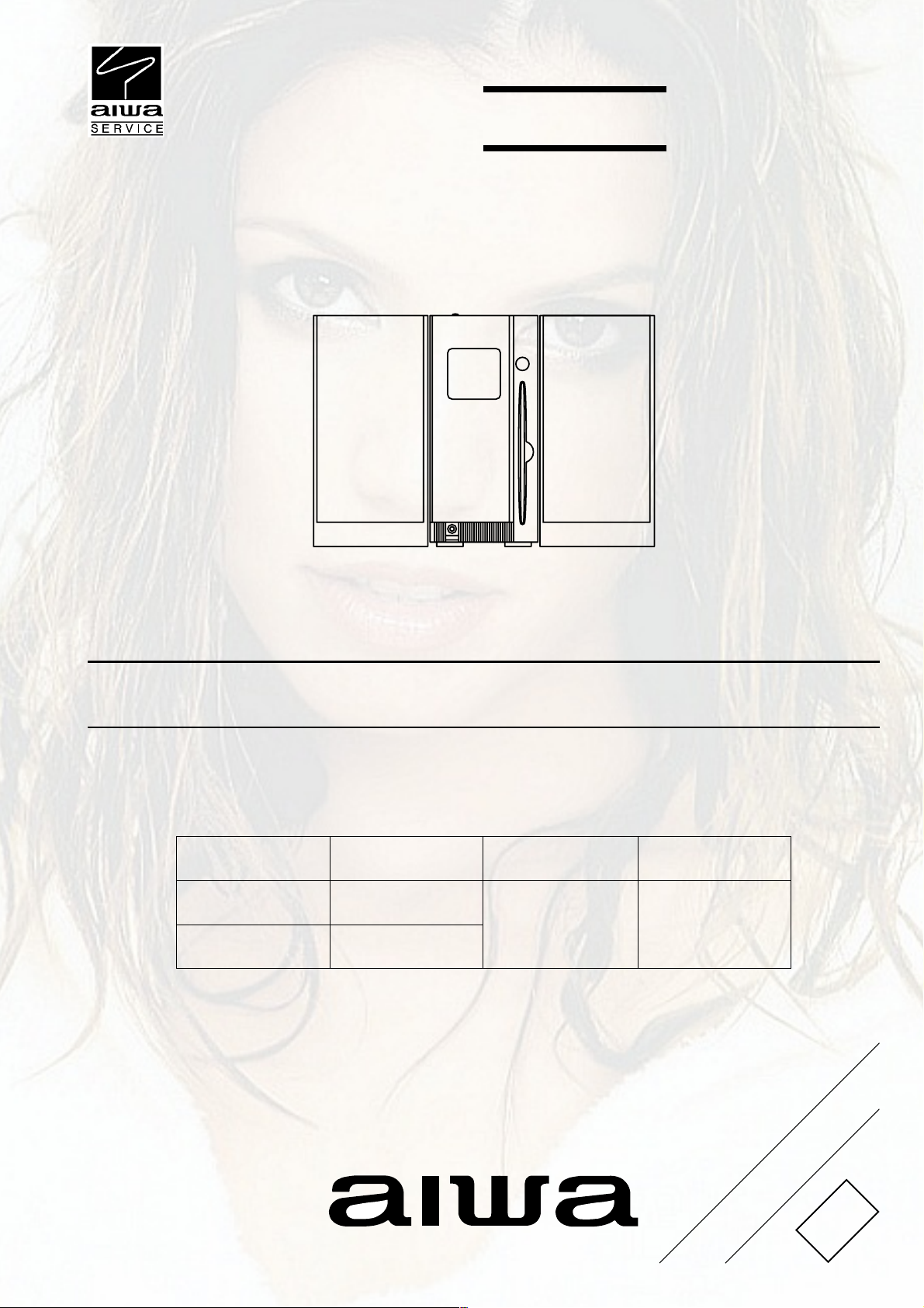
XR-MS5
K
XR-MS6
EZ
SERVICE MANUAL
COMPACT DISC
STEREO SYSTEM
SYSTEM
This Service Manual is the Revision Publishing and replaces Simple Manual
(S/M Code No. 09-012-441-8T2).
CD
CASSEIVER
CXLMS5XRMS5
CXLMS6XRMS6
BASIC CD MECHANISM : AZG-X A1NM
SPEAKER
SXLMS5
REMOTE
CONTROLLER
RCBAT01
S/M Code No. 09-015-441-8R2
REVISION
DATA
Page 2

TABLE OF CONTENTS
SPECIFICATIONS ...............................................................................................................................................................3
PROTECTION OF EYES FROM LASER BEAM DURING SERVICING ........................................................................ 4
PRECAUTION TO REPLACE OPTICAL BLOCK .............................................................................................................4
DISASSEMBLY INSTRUCTIONS 1............................................................................................................................5 ~ 7
DISASSEMBLY INSTRUCTIONS 2..........................................................................................................................8 ~ 13
ELECTRICAL MAIN PARTS LIST ...........................................................................................................................14 ~ 17
CHIP RESISTOR PART CODE ....................................................................................................................................... 17
TRANSISTOR ILLUSTRATION......................................................................................................................................... 18
WIRING 1 (MAIN / HP J) ............................................................................................................................................. 19
SCHEMATIC DIAGRAM 1 (MAIN : 1 / 2 / HP J) .........................................................................................................20
SCHEMATIC DIAGRAM 2 (MAIN : 2 / 2 <MICON SECTION>) ....................................................................................21
WIRING 2 (FRONT / AMP) ............................................................................................................................................22
SCHEMATIC DIAGRAM 3 (FRONT) .............................................................................................................................23
SCHEMATIC DIAGRAM 4 (AMP) .................................................................................................................................. 24
WIRING 3 (TUNER) .......................................................................................................................................................25
SCHEMATIC DIAGRAM 5 (TUNER) .............................................................................................................................26
WIRING 4 (AC 2M / PT MAIN) ..................................................................................................................................... 27
SCHEMATIC DIAGRAM 6 (AC 2M / PT MAIN) ...........................................................................................................28
WIRING 5 (CD) <1 / 2> ................................................................................................................................................. 29
WIRING 5 (CD) <2 / 2> ................................................................................................................................................. 30
SCHEMATIC DIAGRAM 7 (CD) ....................................................................................................................................31
FL (9 ST 24GONK) GRID ASSIGNMENT / ANODE CONNECTION / PIN CONNECTION ............................... 32 ~ 35
IC BLOCK DIAGRAM ...............................................................................................................................................36 ~ 38
IC DESCRIPTION ..................................................................................................................................................... 39 ~ 45
ADJUSTMENT (TUNER / MICON) .................................................................................................................................... 46
CD TEST MODE ......................................................................................................................................................47 ~ 48
MECHANICAL PARTS ARRANGEMENT ................................................................................................................49 ~ 53
MECHANICAL PARTS LIST 1 / 1 .................................................................................................................................... 54
COLOR NAME TABLE .....................................................................................................................................................54
CD MECHANISM EXPLODED VIEW 1 / 1 .....................................................................................................................55
CD MECHANISM PARTS LIST 1 / 1 ..............................................................................................................................56
GENERAL SPEAKER DISASSEMBLY INSTRUCTIONS (FOR REFERENCE) ............................................................ 57
SPEAKER PARTS LIST (SX LMS5) <YJ1BN> ............................................................................................................. 58
ACCESSORIES / PACKAGE LIST .................................................................................................................................... 58
2
Page 3

SPECIFICATIONS
MAIN UNIT CX-LMS5/CX-LMS6
TUNER
FM tuning range 87.5 MHz to 108 MHz
FM usable sensitivity (IHF) 16.8 dBf
FM antenna terminal 75 ohms (unbalanced)
MW tuning range 531 kHz to 1602 kHz (9 kHz step)
530 kHz to 1710 kHz (10 kHz step)
MW usable sensitivity 350 µV/m
LW tuning range 144 kHz to 290 kHz
LW usable sensitivity 1400 µV/m
MW/LW antenna Loop antenna
AMPLIFIER
Power output Rated: 12 W + 12 W
(6 ohms, T.H.D. 1 %, 1 kHz/DIN 45500)
Reference: 15 W + 15 W
(6 ohms, T.H.D. 10 %, 1 kHz/DIN 45324)
DIN MUSIC POWER
22 W + 22 W
Input VIDEO/AUX: 600 mV
Outputs SPEAKERS: 6 ohms or more
PHONES: 16 ohms or more
SUPER WOOFER 0.85 V
DIGITAL OUT (OPTICAL) jack
LINE OUT jack
CD PLAYER
Laser Semiconductor laser (l = 780 nm)
D/A converter 1 bit dual
Signal-to-noise ratio 85 dB (1 kHz, 0 dB)
Harmonic distortion 0.08 % (1 kHz, 0 dB)
Wow and flutter Unmeasurable
GENERAL
Power requirements 230 V AC, 50 Hz
Power consumption 45 W
Power consumption in standby mode
With ECO mode on: 1.3 W
With ECO mode off: 12 W
Dimensions (W x H x D) 100.0 x 205.0 x 292.5 mm
Weight 3.5 kg
SPEAKER SYSTEM SX-LMS5
Speaker system 2 way, bass reflex (magnetic shielded)
Speaker units Woofer: 85 mm cone
Tweeter: 22 mm dome
Impedance 6 ohms
Dimensions (W x H x D) 100 x 210 x 185 mm
Weight 1.5 kg
Design and specifications are subject to change without notice.
3
Page 4

PROTECTION OF EYES FROM LASER BEAM DURING SERVICING
This set employs laser. Therefore, be sure to follow carefully the
instructions below when servicing.
WARNING!!
WHEN SERVICING, DO NOT APPROACH THE LASER
EXIT WITH THE EYE TOO CLOSELY. IN CASE IT IS
NECESSARY TO CONFIRM LASER BEAM EMISSION.
BE SURE TO OBSERVE FROM A DISTANCE OF MORE
THAN 30cm FROM THE SURFACE OF THE OBJECTIVE
LENS ON THE OPTICAL PICK-UP BLOCK.
Caution: Invisible laser radiation when
open and interlocks defeated avoid
exposure to beam.
Advarsel: Usynlig laserståling ved åbning,
når sikkerhedsafbrydere er ude af funktion.
Undgå udsættelse for stråling.
VAROITUS!
Laiteen Käyttäminen muulla kuin tässä käyttöohjeessa
mainitulla tavalla saataa altistaa käyt-täjän
turvallisuusluokan 1 ylittävälle näkymättömälle
lasersäteilylle.
VARNING!
Om apparaten används på annat sätt än vad som
specificeras i denna bruksanvising, kan användaren
utsättas för osynling laserstrålning, som överskrider
gränsen för laserklass 1.
CAUTION
Use of controls or adjustments or performance of procedures other than those specified herin may result in
hazardous radiation exposure.
ATTENTION
Lutillisation de commandes, réglages ou procédures
autres que ceux spécifiés peut entraîner une dangereuse
exposition aux radiations.
ADVARSEL
Usynlig laserståling ved åbning, når sikkerhedsafbrydereer
ude af funktion. Undgå udsættelse for stråling.
This Compact Disc player is classified as a CLASS 1
LASER product.
The CLASS 1 LASER PRODUCT label is located on the
rear exterior.
CLASS 1 LASER PRODUCT
KLASSE 1 LASER PRODUKT
LUOKAN 1 LASER LAITE
KLASS 1 LASER APPARAT
Precaution to replace Optical block
(KSM 900AMA)
Body or clothes electrostatic potential could
ruin laser diode in the optical block. Be sure
ground body and workbench, and use care
the clothes do not touch the diode.
1) After the connection, remove solder
shown in the right figure.
PICKUP Assy PWB
Solder
16 10 9 1
4
Page 5
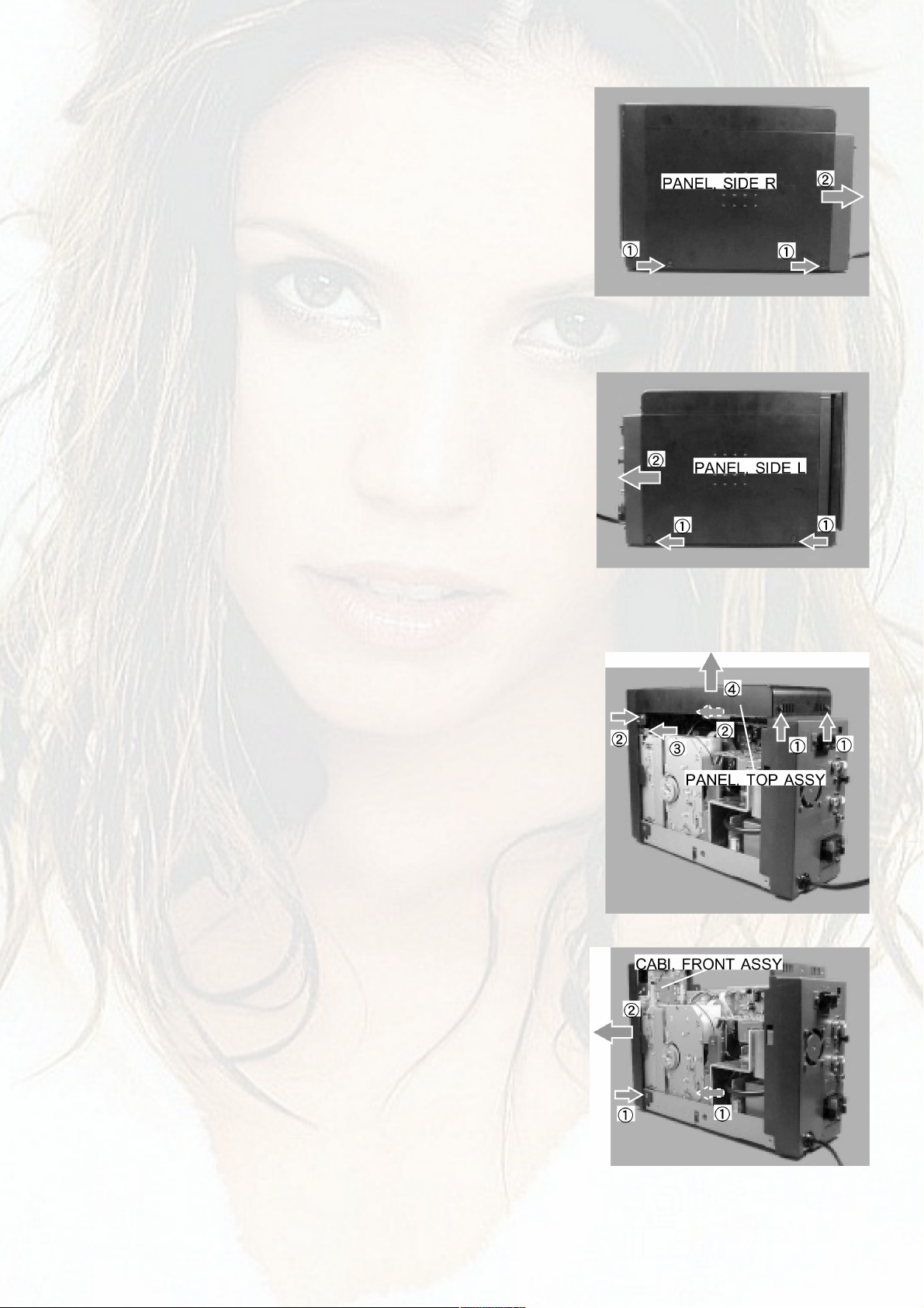
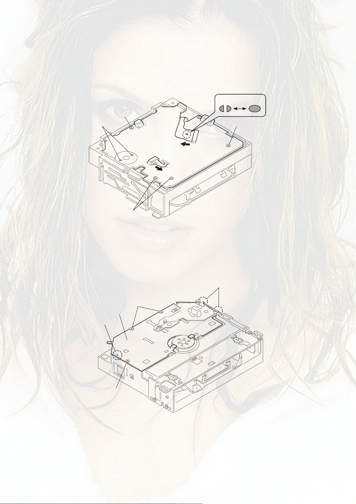
DISASSEMBLY INSTRUCTIONS 1
1. DISASSEMBLY OF AZG-X AND SERVICE POSITION
1) Disassembling the AZG-X
(1) Remove the two screws (1) and remove the PANEL, SIDE R (2).
(2) Remove the two screws (1) and remove the PANEL, SIDE L (2).
(3) Remove five screws (1), (2) and (3), and remove the PANEL, TOP
ASSY (4).
(4) Remove the two screws (1) and remove the CABI, FRONT ASSY.
5
Page 6
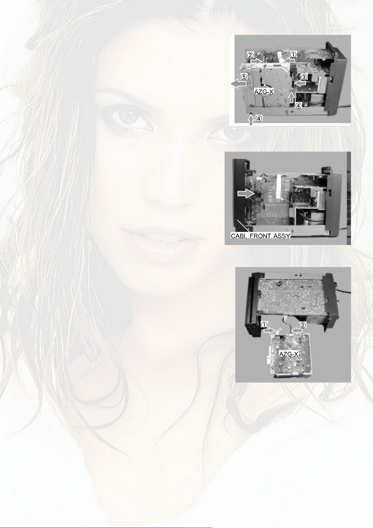
(5) Remove the FFC (1) and remove the two connectors (2) and (3).
Remove the two screws (4) and remove the AZG-X (5).
2) CD Service Position
(1) Install the CABI, FRONT ASSY.
(2) Connect the FFC (1) to the connector (2).
6
Page 7
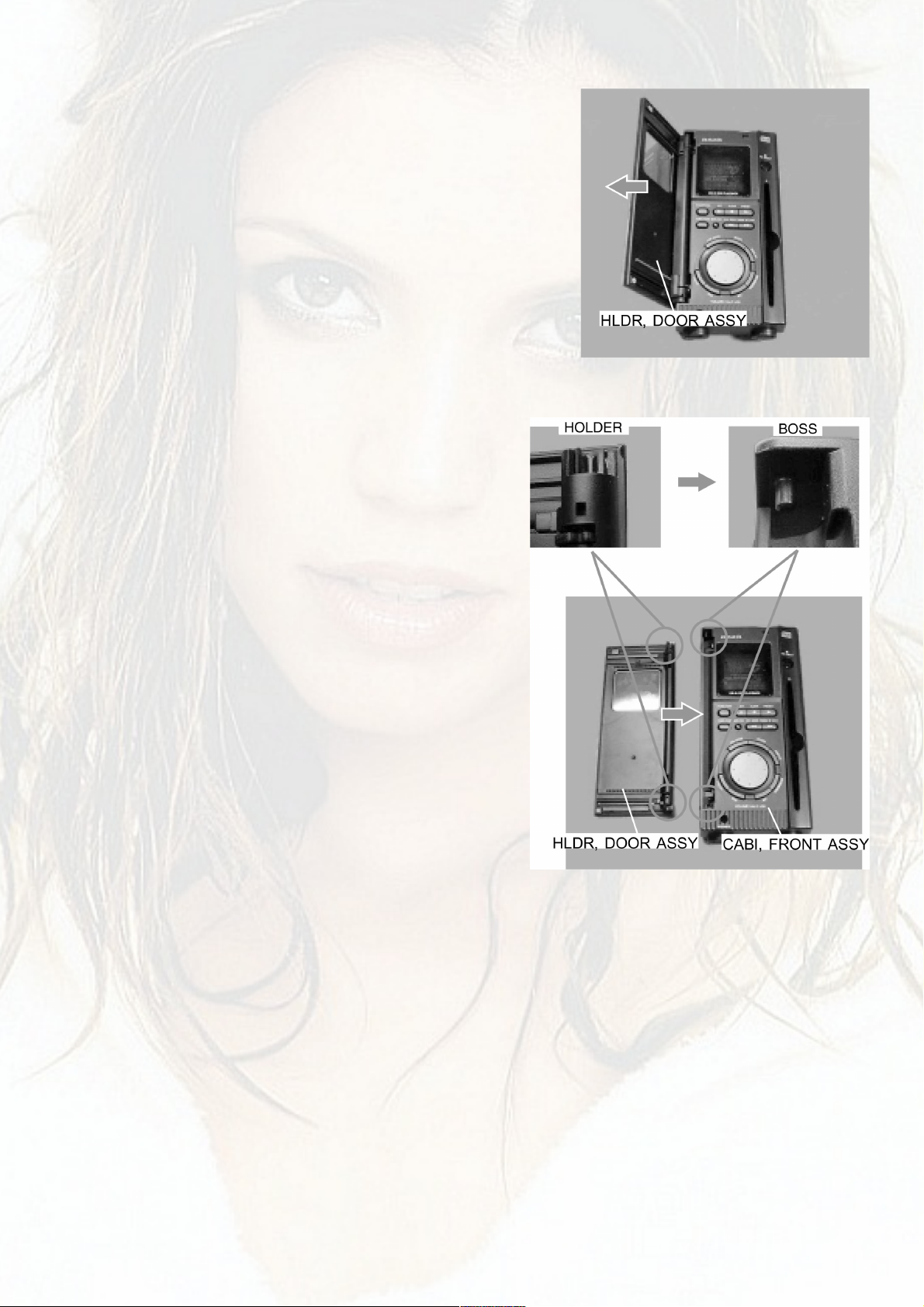
2. DISASSEMBLY OF HLDR, DOOR ASSY
1) Open the HLDR, DOOR ASSY and pull it in the direction of
the arrow.
3. INSTALLATION OF HLDR, DOOR ASSY
1) Insert the HLDR, DOOR ASSY in the direction of the arrow.
(Insert the boss of the CABI, FRONT ASSY into the holder of
the HLDR, DOOR ASSY.)
7
Page 8
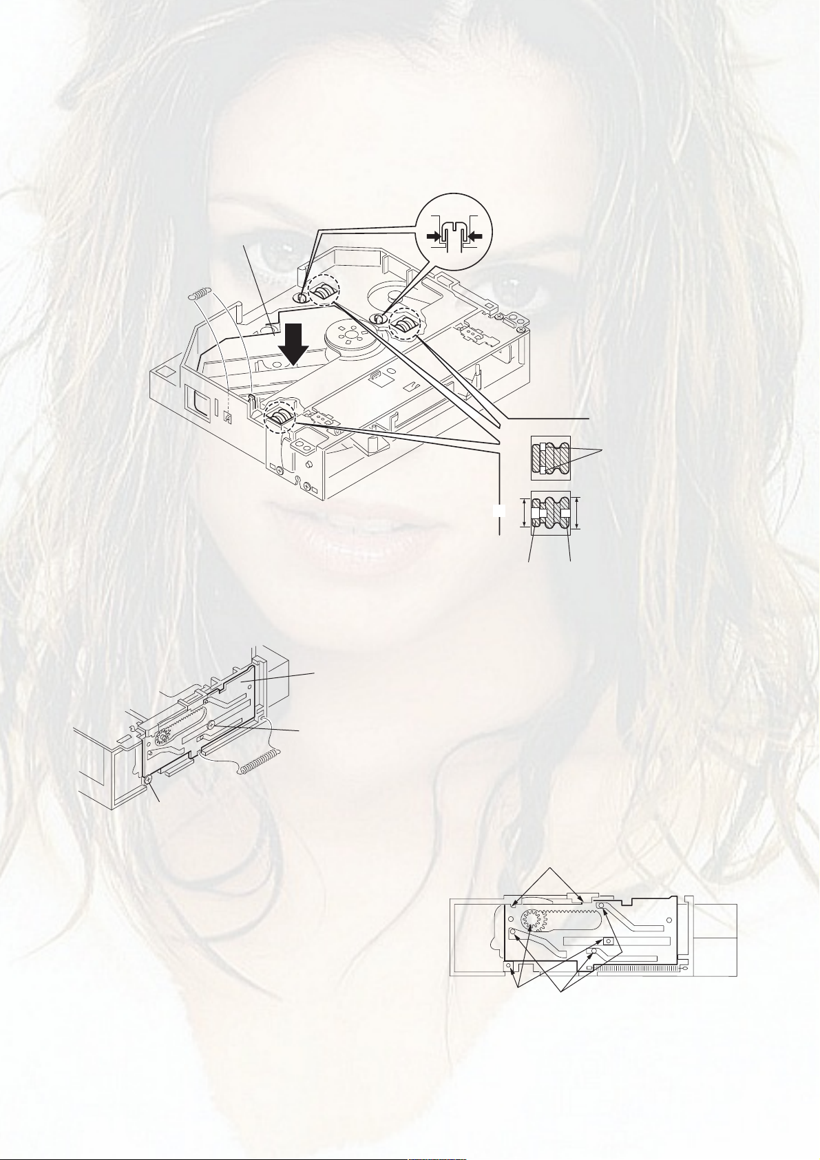
DISASSEMBLY INSTRUCTIONS 2
DISASSEMBLY AND REASSEMBLY OF AZG-X (30) AND AZG-A (10)
1) Removing the PWB, CD
(1) Short the shorting-lands on the flexible card wire of the optical pickup by soldering.
(2) Disconnect wires from the connectors CN706 and CN707.
(3) Remove soldering of the loading motor.
(4) Remove the four screws A and remove the PWB, CD.
* To reassemble it, reverse the steps of disassembling as described above.
4) A
3)
CN707
CN706
2)
2)
1) Shorting-land of pickup
4) A
4) A
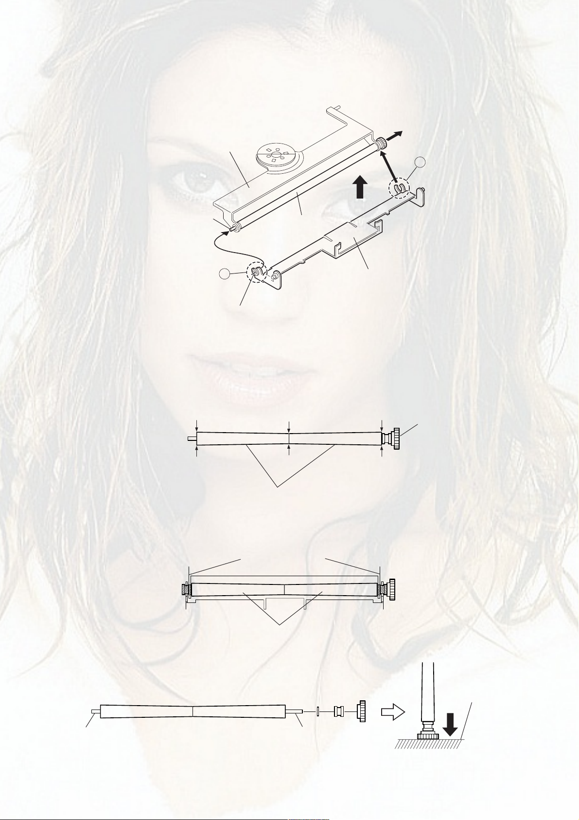
2) Removing the PLATE CD RE
(1) Remove the three screws A and remove the PLATE CD RE.
* When reassemble it, be careful of the slits and boss.
A
PLATE CD RE
* BOSS
* SLIT
A
8
Page 9
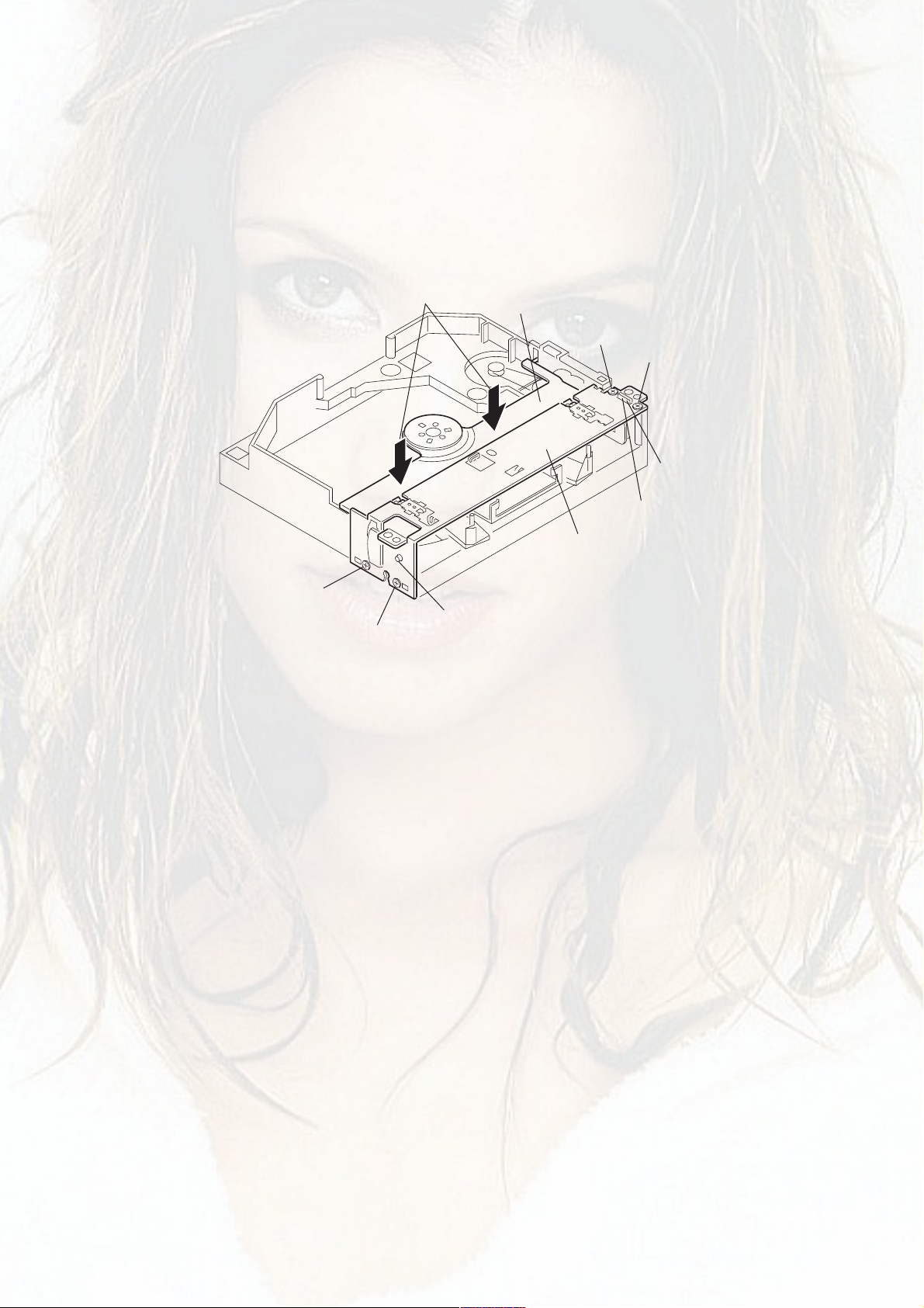
3) Removing the CD MECHA ASSY
(1) Remove the SPR-E, MECHA.
(2) Remove the hooks (at two positions) of the HOLDER MECHA and push down the CD mechanism and
remove the CD mechanism.
* When reassembling it, align the positions of the rubber dampers and the damper hooks as shown.
2) HOOK
CD MECHA
1) SPR-E, MECHA
Be careful to align them
when reassembling it.
Damper hook
4) Removing the PLT, SLIDER
(1) Remove the SPR-E, SLIDER.
(2) Remove the two screws A and remove the PLT, SLIDER.
PLT, SLIDER
A
1) SPR-E, SLIDER
A
Reassembling the PLT, SLIDE
(1) Insert it inside the two base hooks.
(2) Align the position of the three shafts.
(3) Align the position of the gear and the screw boss at two positions.
(4) Fix them with two screws A.
SMALL
LARGE
BOSS
LARGE
SMALL
BOSS
1)
9
3)
2)
Page 10
5) Removing the PLT, CD FR and LVR, ROLLER ASSY
(1) Push down the LVR, ROLLER ASSY in the direction of the arrow.
(2) Remove the four screws A.
(3) Bend the mechanism and remove the boss.
(4) Remove the PLT, CD FR.
(5) Remove the LVR, ROLLER ASSY.
Reassembling the PLT, CD FR
* Reassemble it in the state that the LVR, ROLLER ASSY is being pushed down.
* Insert the SHAFT into the hole of PLT, CD FR and attach it to boss.
1)
A
Assembling shaft
A
LVR, ROLLER ASSY
A
A
3)
Assembling boss
PLT, CD FR
10
Page 11
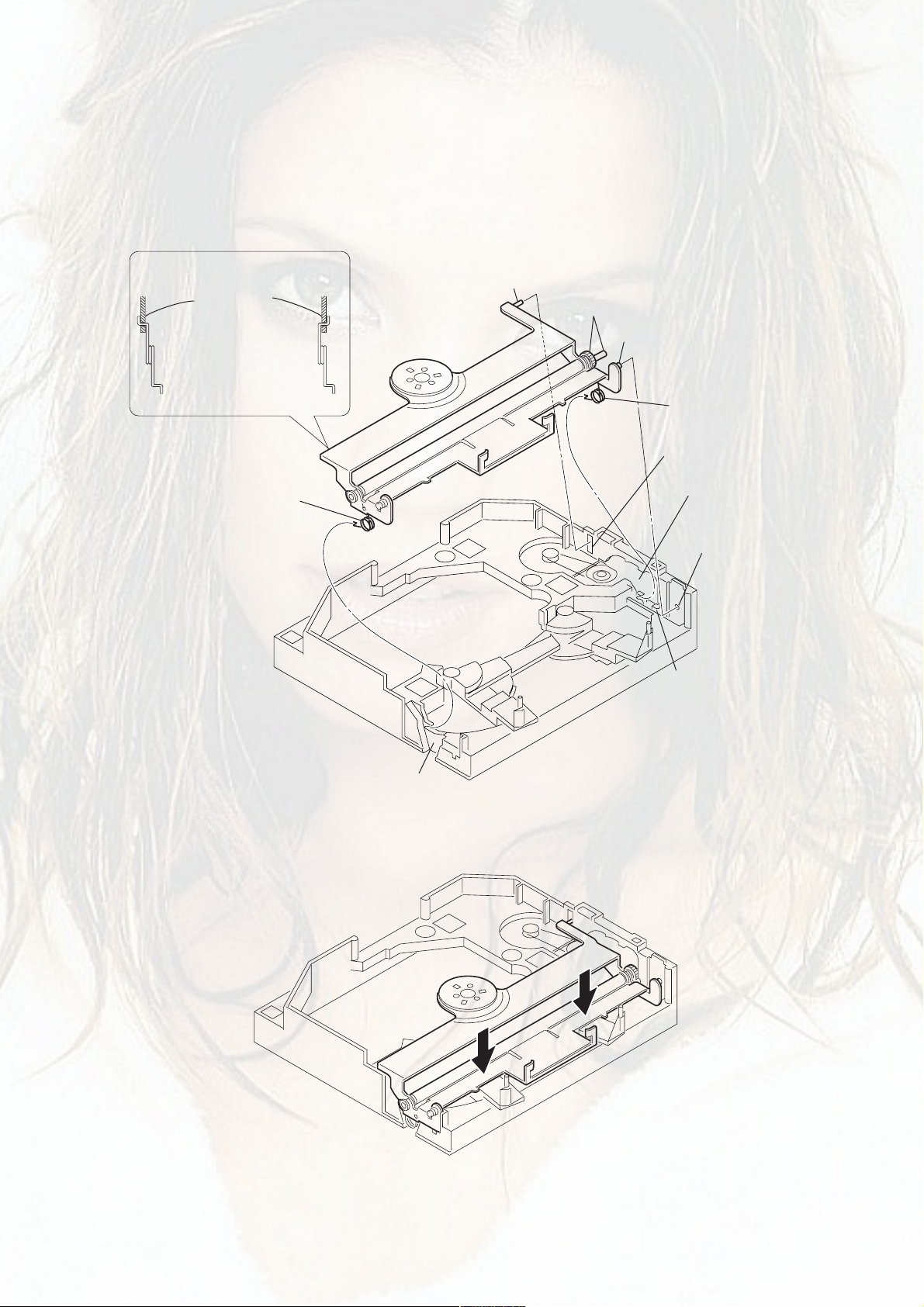
6) Removing the LVR, ROLLER ASSY
(1) Insert the LVR, ROLLER ASSY L and R into the HLDR ASSY CLAMP.
(2) Insert the SHAFT A into the BASE HOLE A.
(3) Insert the GEAR,SHAFT B into BASE HOLE B.
(4) Insert the SPRINGs C1 and C2 into the BASE SLITs C1' and C2'.
(5) While pushing down the LVR, ROLLER ASSY, insert the SHAFT D into the BASE HOLE D.
(6) The LVR, ROLLER is fixed at the specified position as shown.
1) SPR-T, ROLLER L, R
HLDR ASSY
CLAMP
2) SHAFT A
3) GEAR, SHAFT B
5) SHAFT D
4) SPRING C1
2) BASE HOLE A’
4) SPRING C2
6)
3) BASE HOLE B’
5) BASE HOLE D’
4) BASE SLIT C1’
4) BASE SLIT C2’
11
Page 12
7) Disassembling the LVR, ROLLER ASSY
(1) Push the HLDR ASSY CLAMP and release the lock at the (A) position.
(2) Remove the SHAFT ROLLER from the CLR ROLLER and remove the LVR, ROLLER ASSY (B).
(3) Remove the SHAFT ROLLER and remove the ROLLER RUBBER.
HLDR ASSY CLAMP
1)
3)
A
SHAFT ROLLER
2)
B
CLR ROLLER
ROLLER RUBBER
Reassembling the LVR, ROLLER ASSY
Reassemble it by reversing the order of disassembling starting from 3), 2) and then 1).
Perform the following checks during assembling.
At step 3), reassemble it as shown below.
LARGE
ROLLER RUBBER
SMALL
LVR, ASSY ROLLER
SHAFT ROLLER
LARGE
At step 2), attach (B) and (A) as shown below.
* Reassemble the SHAFT ROLLER as shown below.
SHORER LONGER
HLDR ASSY CLAMP
ROLLER RUBBER
FLAT BASE
12
Page 13

8) Removing the MOTOR ASSY
(1) Remove the two screws A and remove the MOTOR.
Reassembling MOTOR ASSY
(1) Attach the MOTOR and PULLEY. MOT as shown below.
(2) Align direction of the MOTOR ASSY label and fix it with the two screws A.
LABEL
A
A
MOT, M25E-10
PULLY
MOT
LABEL
FLAT BASE
5.7mm
BOTTOM VIEW
13
Page 14

ELECTRICAL MAIN PARTS LIST
PART NO. DESCRIPTIONREF. NO. KANRI
NO.
IC
8B-CL5-601-010 C-IC,LC876580W-5T99
87-070-246-010 IC,GP1U271X
87-A21-111-040 C-IC,M62495FP
87-017-825-010 IC,GP1F32T
87-A21-695-010 IC,LA1845L
87-A21-928-010 IC,LC72131D-N
87-A20-440-040 C-IC,BU1920FS<EZ>
87-A21-777-040 C-IC,BA6289F
87-A21-513-040 C-IC,BA6998FP
87-A20-547-010 C-IC,CXA1992AR
87-A20-546-010 C-IC,CXD2589Q
87-017-760-080 C-IC,M51943BML
87-017-917-080 IC,BU4066BCF
87-001-792-080 IC,NJM2100M
TRANSISTOR
89-213-702-010 TR,2SB1370E
87-026-245-080 TR,DTC114ES
87-A30-060-080 C-TR,KTC3875GR
87-A30-198-080 TR,KTC3199GR
87-026-610-080 TR,KTC3198GR
87-A30-061-080 C-TR,KTA1504GR
87-A30-234-080 TR,CSC4115BC
87-026-609-080 TR,KTA1266GR
87-A30-087-080 C-FET,2SK2158
87-A30-105-080 C-TR,RT1P 441C
87-A30-047-080 TR,CSD655E
89-112-965-080 TR,2SA1296GR
87-A30-468-080 C-TR,KRC102S-RTK
89-333-266-080 C-TR,2SC3326B
87-A30-190-080 TR,CC5551
87-A30-106-070 C-TR,CMBT5551
87-A30-306-010 TR,2SB1677
87-A30-307-010 TR,2SD2619
87-A30-107-070 C-TR,CMBT5401
87-A30-484-080 C-TR,KRA102S
87-A30-086-040 C-TR,CSD1306E
87-A30-086-070 C-TR,CSD1306E
89-327-143-080 C-TR,2SC2714O
87-A30-489-080 C-TR,KRA107S
89-503-602-080 C-FET,2SK360E
87-A30-075-080 C-TR,2SA1235F
89-113-695-680 C-TR,2SA1369(G/H)
87-A30-288-040 C-TR,DTC114YKA
DIODE
87-017-650-080 DIODE,1SS119
87-017-447-010 DIODE,GBU4DL
87-A40-313-080 C-DIODE,MC2840
87-A40-757-080 ZENER,UZ7.5BSC
87-A40-764-080 ZENER,UZ10BSC
87-A40-270-080 C-DIODE,MC2838
87-070-274-080 DIODE,1N4003 SEM
87-A40-778-080 ZENER,UZ30BSD
87-A40-504-040 C-DIODE,KDS184
87-A40-505-040 C-DIODE,KDS181
87-A40-768-080 ZENER,UZ16BSA
87-A40-747-080 ZENER,UZ5.1BSB
87-A40-748-080 ZENER,UZ5.6BSA
87-A40-739-080 ZENER,UZ2.7BSA
87-020-465-080 DIODE,1SS133
87-017-149-080 ZENER,HZS6A2L
MAIN C.B
C3 87-010-831-080 C-CAP,U,0.1-16F
DESCRIPTIONREF. NO. KANRI
PART NO.
NO.
C4 87-010-831-080 C-CAP,U,0.1-16F
C5 87-010-831-080 C-CAP,U,0.1-16F
C6 87-010-831-080 C-CAP,U,0.1-16F
C7 87-A10-520-000 CAP,E 3300-35 M SMG
C8 87-010-831-080 C-CAP,U,0.1-16F
C10 87-016-051-000 CAP,E 2200-35 M SMG
C11 87-010-374-040 CAP,E 47-10
C14 87-010-221-040 CAP,E 470-10 SME
C26 87-010-831-080 C-CAP,U,0.1-16F
C27 87-012-270-080 C-CAP,U 470P-50
C29 87-010-112-040 CAP,E 100-16 M 11L SME
C30 87-010-235-080 CAP,E 470-16 M 11L SME
C31 87-010-235-080 CAP,E 470-16 M SME
C41 87-010-385-040 CAP,E 220-25 SME
C42 87-A12-095-040 CAP,E 100-50 SME
C43 87-010-385-040 CAP,E 220-25 SME
C44 87-A12-095-040 CAP,E 100-50 SMG
C45 87-010-430-080 CAP, ELECT 100-63
C46 87-010-263-040 CAP,E 100-10
C48 87-010-408-040 CAP,E 47-50 SME
C61 87-010-374-040 CAP,E 47-10
C62 87-010-496-040 CAP,E 3.3-50 GAS
C91 87-010-071-040 CAP,E 1-50 M 5L SRE
C92 87-010-391-040 CAP,E 10-35 M 11L SME
C93 87-010-553-040 CAP,E 47-16 GAS
C101 87-010-371-040 CAP,E 470-6.3
C103 87-010-831-080 C-CAP,U,0.1-16F
C104 87-012-287-080 C-CAP,U 0.015-25 F
C105 87-012-287-080 C-CAP,U 0.015-25 F
C106 87-A10-827-080 C-CAP,U 0.47-6.3 K B
C108 87-012-178-080 C-CAP,U 18P-50 CH
C109 87-012-199-080 C-CAP,U 220P-50
C114 87-012-278-080 C-CAP,U 2200P-50 B
C116 87-010-831-080 C-CAP,U,0.1-16F
C117 87-010-831-080 C-CAP,U,0.1-16F
C118 87-010-831-080 C-CAP,U,0.1-16F
C129 87-012-184-080 C-CAP,U 33P-50 CH
C130 87-012-274-080 CHIP CAP,U 1000P-50B
C202 87-012-195-080 C-CAP,U 100P-50 J CH
C222 87-010-221-040 CAP,E 470-10 M SME
C225 87-010-831-080 C-CAP,U,0.1-16F
C227 87-010-831-080 C-CAP,U,0.1-16F
C229 87-010-831-080 C-CAP,U,0.1-16F
C230 87-010-831-080 C-CAP,U,0.1-16F
C231 87-010-831-080 C-CAP,U,0.1-16F
C232 87-010-831-080 C-CAP,U,0.1-16F
C233 87-012-287-080 C-CAP,U 0.015-25 F
C234 87-012-287-080 C-CAP,U 0.015-25 F
C601 87-010-494-040 CAP,E 1-50 M 5L SRE
C602 87-010-494-040 CAP,E 1-50 M 5L SRE
C605 87-012-278-080 C-CAP,U 2200P-50 B
C606 87-012-278-080 C-CAP,U 2200P-50 B
C607 87-012-287-080 C-CAP,U 0.015-25 F
C608 87-012-287-080 C-CAP,U 0.015-25 F
C609 87-010-491-040 CAP,E 0.22-50 GAS
C610 87-010-491-040 CAP,E 0.22-50 GAS
C611 87-010-491-040 CAP,E 0.22-50 GAS
C612 87-010-491-040 CAP,E 0.22-50 GAS
C613 87-010-380-040 CAP,E 47-16 SME
C614 87-010-380-040 CAP,E 47-16 SME
C615 87-012-172-080 CAPACITOR CHIP U 10P CH
C616 87-012-199-080 C-CAP,U 220P-50 J CH
C617 87-012-199-080 C-CAP,U 220P-50 J CH
C631 87-010-401-040 CAP,E 1-50 SME
C632 87-010-401-040 CAP,E 1-50 SME
C641 87-010-831-080 C-CAP,U,0.1-16F
C643 87-A10-047-080 C-CAP,U 1-10 Z F
C644 87-010-831-080 C-CAP,U,0.1-16F
C663 87-010-831-080 C-CAP,U 0.1-16 Z F
C664 87-010-831-080 C-CAP,U 0.1-16 Z F
14
Page 15

PART NO. DESCRIPTIONREF. NO. KANRI
NO.
C669 87-012-199-080 C-CAP,U 220P-50 J CH
C670 87-012-199-080 C-CAP,U 220P-50 J CH
C703 87-010-831-080 C-CAP,U,0.1-16F
C707 87-010-831-080 C-CAP,U,0.1-16F
C869 87-012-286-080 C-CAP,U 0.01-25 K B<EZ>
C870 87-012-274-080 C-CAP,U 1000P-50 K B<EZ>
C871 87-012-199-080 C-CAP,U 220P-50 J CH<EZ>
C872 87-012-199-080 C-CAP,U 220P-50 J CH<EZ>
C873 87-012-270-080 C-CAP,U 470P-50 K B<EZ>
C874 87-010-075-080 CAP,E 10-16 M 5L SRE<EZ>
C875 87-010-831-080 C-CAP,U 0.1-16 Z F<EZ>
C876 87-010-075-080 CAP,E 10-16 M 5L SRE<EZ>
C877 87-012-286-080 C-CAP,U 0.01-25 K B<EZ>
C878 87-012-184-080 C-CAP,U 33P-50 J CH<EZ>
C879 87-012-180-080 C-CAP,U 22P-50 J CH<EZ>
CN1 87-009-195-010 CONN,5P V WHT EH
CN91 87-A60-619-010 CONN,2P V 2MM JMT
CN201 87-A60-996-010 CONN,13P V BLK TAC-L13X-A3
CN203 87-099-564-010 CONN,4P TUC-P4P-B1
CN205 87-A60-685-010 CONN,4P H WHT EH
CN701 87-A60-619-010 CONN,2P V 2MM JMT
CN901 87-A60-769-010 CONN,14P B TMC-D(X)
CN903 87-A60-189-010 CONN,16P V TUC-P16P-B1
CN905 87-A61-366-010 CONN,10P V BLK FMN-BTRK
CNA2 88-805-030-820 CONN ASSY,3P 80
CNA4 8B-CL5-606-010 CONN ASSY,6P PH CD POWER
CNA206 8B-CJ5-615-010 CONN ASSY,4P EH HPJ
CNA701 8B-CL5-609-010 CONN ASSY,2P SHLD 250
FFC710 8B-CL5-607-010 FFC,10P 1.10-200
J201 87-033-240-010 TERMINAL,4P HSP-324V1-05
J202 87-099-801-010 JACK,PIN 1P BLK W/O SW
J601 87-A60-881-010 JACK,PIN 2P MSP 242V05 PBSN
J602 87-A60-881-010 JACK,PIN 2P MSP 242V05 PBSN
JW193 87-008-372-080 FLTR,EMI BL01 RN1
JW205 87-008-372-080 FLTR,EMI BL01 RN1
L101 87-A50-333-010 COIL,OSC 9.43MHZ
L201 87-003-383-010 COIL,1UH K
L202 87-003-383-010 COIL,1UH K
L821 87-A50-027-010 COIL,1 POLE MPX(TOK)
L822 87-A50-027-010 COIL,1 POLE MPX(TOK)
L861 87-005-847-080 COIL,2.2UH K CECS<EZ>
W201 8B-CL5-608-010 F-CABLE,2P 2.5 200MM
WH201 87-A90-506-010 HLDR,WIRE 2.5-2P
WH202 87-A90-506-010 HLDR,WIRE 2.5-2P
X861 87-A70-091-010 VIB,XTAL 4.332MHZ CSA-309<EZ>
FRONT C.B
C102 87-010-075-040 CAP,E 10-16 5L
C103 87-012-268-080 C-CAP,U 330P-50 B
C104 87-010-421-040 CAP,E 4.7-50 5L
C105 87-010-421-040 CAP,E 4.7-50 5L
C106 87-A10-797-040 CAP,E 47-35 M 5L SRM
C107 87-A12-317-080 C-CAP,U 0.1-50 Z F
C108 87-012-286-080 C-CAP,U 0.01-25
C109 87-012-286-080 C-CAP,U 0.01-25
C110 87-010-831-080 C-CAP,U,0.1-16F
C111 87-A12-317-080 C-CAP,U 0.1-50 Z F
CN101 87-A60-777-010 CONN,14P B TMC-D(P)
FL101 8B-CL5-615-010 FL,9-ST-24GONK
LED101 87-A40-317-080 LED,SLR-342VCT31 RED
R102 87-022-239-080 C-RES U 10K-1/16WF
R103 87-022-239-080 C-RES U 10K-1/16WF
S101 87-A92-079-010 SW,RTRY RE12303PVB15FINA -JOG
S102 87-A90-095-080 SW,TACT EVQ11G04M
S103 87-A90-095-080 SW,TACT EVQ11G04M
S104 87-A90-095-080 SW,TACT EVQ11G04M
S105 87-A90-095-080 SW,TACT EVQ11G04M
S106 87-A90-095-080 SW,TACT EVQ11G04M
S107 87-A90-095-080 SW,TACT EVQ11G04M
DESCRIPTIONREF. NO. KANRI
PART NO.
NO.
S108 87-A90-095-080 SW,TACT EVQ11G04M
S109 87-A90-095-080 SW,TACT EVQ11G04M
S110 87-A90-095-080 SW,TACT EVQ11G04M
S111 87-A90-095-080 SW,TACT EVQ11G04M
S112 87-A90-095-080 SW,TACT EVQ11G04M
S113 87-A90-095-080 SW,TACT EVQ11G04M
S114 87-A90-095-080 SW,TACT EVQ11G04M
S115 87-A90-095-080 SW,TACT EVQ11G04M
S116 87-A90-095-080 SW,TACT EVQ11G04M
S117 87-A91-525-080 SW,TACT SKQNLA
S118 87-036-252-010 SW,PUSH SPPB 51
S119 87-A90-095-080 SW,TACT EVQ11G04M
AMP C.B
C201 87-012-277-080 C-CAP,U 1800P-50 B
C202 87-012-277-080 C-CAP,U 1800P-50 B
C203 87-010-400-080 CAP, ELECT 0.47-50V
C204 87-010-400-080 CAP, ELECT 0.47-50V
C207 87-010-401-080 CAP, ELECT 1-50V
C208 87-010-401-080 CAP, ELECT 1-50V
C211 87-010-383-080 CAP, ELECT 33-25V
C212 87-010-383-080 CAP, ELECT 33-25V
C213 87-012-266-080 C-CAP,U 220P-50 B
C214 87-012-266-080 C-CAP,U 220P-50 B
C217 87-A12-317-080 C-CAP,U 0.1-50 Z F
C218 87-A12-317-080 C-CAP,U 0.1-50 Z F
C219 87-012-286-080 C-CAP,U 0.01-25
C220 87-012-286-080 C-CAP,U 0.01-25
C221 87-010-544-080 CAP, ELECT 0.1-50V
C225 87-A12-317-080 C-CAP,U 0.1-50 Z F
C226 87-A12-317-080 C-CAP,U 0.1-50 Z F
C228 87-010-544-080 CAP, ELECT 0.1-50V
C298 87-012-282-080 C-CAP,U 4700P-50
C299 87-012-286-080 C-CAP,U 0.01-25
CN202 87-A61-011-010 CONN,13P H BLK TAC-L13P-A3
R229 87-A00-986-080 RES,M/F 0.22-1W J
R230 87-A00-986-080 RES,M/F 0.22-1W J
R231 87-A00-986-080 RES,M/F 0.22-1W J
R232 87-A00-986-080 RES,M/F 0.22-1W J
TH201 87-A91-042-080 C-THMS,100K 55001
TH202 87-A91-042-080 C-THMS,100K 55001
TUNER C.B
C772 87-012-286-080 C-CAP,U 0.01-25 K B
C786 87-012-286-080 C-CAP,U 0.01-25 K B
C788 87-012-167-080 C-CAP,U 5P-50 CH
C789 87-A11-228-080 C-CAP,U 0.027-25 K B
C790 87-A11-228-080 C-CAP,U 0.027-25 K B
C791 87-010-831-080 C-CAP,U,0.1-16F
C792 87-012-286-080 C-CAP,U 0.01-25 K B
C793 87-A11-056-080 C-CAP,U 1-10 Z F
C795 87-012-286-080 C-CAP,U 0.01-25 K B
C798 87-010-831-080 C-CAP,U 0.1-16 Z F
C799 87-010-982-040 CAP,E 33-25 GAS
C800 87-012-191-080 C-CAP,U 68P-50 J CH
C801 87-A11-056-080 C-CAP,U 1-10 Z F
C802 87-010-829-080 CAP, U 0.047-16
C804 87-010-555-040 CAP,E 100-10 GAS
C807 87-A10-463-080 C-CAP,U 0.47-10 Z F
C808 87-A11-056-080 C-CAP,U 1-10 Z F
C809 87-A11-056-080 C-CAP,U 1-10 Z F
C815 87-A10-463-080 C-CAP,U 0.47-10 Z F
C816 87-A10-463-080 C-CAP,U 0.47-10 Z F
C818 87-012-276-080 C-CAP,U 1500P-50 K B
C821 87-A11-063-080 C-CAP,S 4.7-10 Z F
C822 87-012-270-080 C-CAP,U 470P-50 K B
C823 87-012-274-080 C-CAP,U 1000P-50 K B
C824 87-A11-063-080 C-CAP,S 4.7-10 Z F
15
Page 16

PART NO. DESCRIPTIONREF. NO. KANRI
DESCRIPTIONREF. NO. KANRI
NO.
C825 87-A11-317-080 C-CAP,U 0.068U-16 K B
C831 87-010-552-040 CAP,E 22-16 GAS
C837 87-A12-022-080 C-CAP,U 0.22-16 Z F
C842 87-010-831-080 C-CAP,U 0.1-16 Z F
C844 87-012-286-080 C-CAP,U 0.01-25 K B
C850 87-A11-056-080 C-CAP,U 1-10 Z F
C851 87-012-286-080 C-CAP,U 0.01-25 K B
C852 87-012-286-080 C-CAP,U 0.01-25 K B
C853 87-012-286-080 C-CAP,U 0.01-25 K B
C859 87-010-831-080 C-CAP,U 0.1-16 Z F
C860 87-012-286-080 C-CAP,U 0.01-25 K B
C901 87-012-162-080 C-CAP,U 1P-50 C CH
C902 87-012-165-080 C-CAP,U 3P-50 C CH
C903 87-012-164-080 C-CAP,U 2P-50 C CH
C904 87-A12-348-080 C-CAP,U 560P-25 J CH
C905 87-012-162-080 C-CAP,U 1P-50 C CH
C906 87-012-172-080 C-CAP,U 10P-50 D CH
C907 87-012-166-080 C-CAP,U 4P-50 C CH
C908 87-012-165-080 C-CAP,U 3P-50 C CH
C909 86-ZA1-615-080 C-CAP,U 680P-25 J CH
C910 87-012-164-080 C-CAP,U 2P-50 C CH
C911 87-012-166-080 C-CAP,U 4P-50 C CH
C912 87-012-195-080 C-CAP,U 100P-50CH
C913 86-ZA1-616-080 C-CAP,U 0.01-50 K B(MUR)
C914 86-ZA1-616-080 C-CAP,U 0.01-50 K B(MUR)
C915 86-ZA1-616-080 C-CAP,U 0.01-50 K B(MUR)
C916 86-ZA1-616-080 C-CAP,U 0.01-50 K B(MUR)
C917 87-012-178-080 C-CAP,U 18P-50 J CH
C918 87-012-172-080 C-CAP,U 10P-50 D CH
C919 87-012-184-080 C-CAP,U 33P-50 J CH
C920 87-012-184-080 C-CAP,U 33P-50 J CH
C921 87-012-180-080 C-CAP,U 22P-50 J CH
C922 87-012-174-080 CAP CHIP CERA SS 12P CHJ
C923 86-ZA1-616-080 C-CAP,U 0.01-50 K B(MUR)
C924 87-012-164-080 C-CAP,U 2P-50 C CH
C925 87-012-164-080 C-CAP,U 2P-50 C CH
C926 86-ZA1-616-080 C-CAP,U 0.01-50 K B(MUR)
C927 87-012-195-080 C-CAP,U 100P-50CH
C942 87-012-167-080 C-CAP,U 5P-50 C CH
C947 87-012-286-080 C-CAP,U 0.01-25 K B
C948 87-012-270-080 C-CAP,U 470P-50 K B
C952 87-012-286-080 C-CAP,U 0.01-25 K B
C957 87-012-174-080 C-CAP,U 12P-50 J CH
C958 87-012-286-080 C-CAP,U 0.01-25 K B
C962 87-A11-056-080 C-CAP,U 1-10 Z F
C963 87-010-831-080 C-CAP,U 0.1-16 Z F
C971 87-010-381-080 CAP, ELECT 330-16V
C972 87-A11-063-080 C-CAP,S 4.7-10 Z F
C973 87-012-286-080 C-CAP,U 0.01-25 K B
C974 87-012-286-080 C-CAP,U 0.01-25 K B
C976 87-010-831-080 C-CAP,U,0.1-16F
C979 87-012-195-080 C-CAP,U 100P-50CH
C981 87-010-553-040 CAP,E 47-16 GAS
C982 87-010-831-080 C-CAP,U,0.1-16F
C983 87-A11-132-080 CAP,TC U 0.01-50 K B
C984 87-012-286-080 C-CAP,U 0.01-25 K B
C985 87-012-195-080 C-CAP,U 100P-50CH
C987 87-012-286-080 C-CAP,U 0.01-25 K B
C989 87-012-286-080 C-CAP,U 0.01-25 K B
C990 87-012-195-080 C-CAP,U 100P-50CH
C991 87-012-182-080 C-CAP,U 27P-50 J CH
C992 87-012-172-080 C-CAP,U 10P-50 D CH
C993 87-012-274-080 CHIP CAP,U 1000P-50B
C994 87-012-195-080 C-CAP,U 100P-50CH
C995 87-012-274-080 CHIP CAP,U 1000P-50B
C996 87-012-195-080 C-CAP,U 100P-50CH
C997 87-010-831-080 C-CAP,U,0.1-16F
C998 87-010-553-040 CAP,E 47-16 GAS
C999 87-012-286-080 C-CAP,U 0.01-25 K B
CF831 87-008-423-010 FLTR,CF SFE10.7MS3G-A
PART NO.
NO.
CF832 82-785-747-010 CF,MS2 GHY,R
CN991 87-A60-650-010 CONN,16P H GRY TUC-P16X-C1
D901 87-A41-048-040 C-VARI-CAP,HVM16-03 TL
D902 87-A41-048-040 C-VARI-CAP,HVM16-03 TL
D903 87-A41-048-040 C-VARI-CAP,HVM16-03 TL
J832 87-A61-534-010 TERMINAL,ANT PAL AJ-2021
J940 87-A60-633-010 CONN,2P H 2.5MM JMT
JW959 87-A11-132-080 CAP,TC U 0.01-50 K B
L801 87-A50-694-010 COIL,FM-DET 2 (COILS)
L802 87-A91-551-010 FLTR,PCFJZH-450 L(TOK)
L811 87-005-847-080 COIL,2.2UH K CECS
L832 87-005-847-080 COIL,2.2UH K CECS
L901 86-ZA1-612-010 COIL,FM ANT/RF-1-Z
L902 86-ZA1-613-010 COIL,FM ANT/RF-2-Z
L903 87-003-098-080 COIL,2.2UH K LAL02
L904 86-ZA1-613-010 COIL,FM ANT/RF-2-Z
L905 86-ZA1-612-010 COIL,FM ANT/RF-1-Z
L906 87-005-847-080 COIL,2.2UH K CECS
L907 86-ZA1-614-010 COIL,FM OSC-Z
L908 88-ZA1-624-010 COIL,FM IFT 7-6.2 (COILS)
L941 87-A50-020-010 COIL,ANT LW(COI) 252KHZ
L942 87-A50-019-010 COIL,OSC LW(COI) 856KHZ
L951 8A-NF8-668-010 COIL,AM PACK 2(TOK)
R790 87-012-286-080 C-CAP,U 0.01-25 KB
TC942 87-A91-774-080 TRIMMER,PLY 30P 6.8X5.4 CDYL
X991 87-A70-061-010 VIB,XTAL 4.500MHZ CSA-309
AC 2M C.B
!
C1 87-A10-479-080 CAP,CER 2200P-250 M E KH
C14 87-010-388-080 CAP ELECT 1000-25V SME
C16 87-010-496-080 CAP,E 3.3-50 5L
!
CN1 87-A60-645-010 CONN,3P V VH
CN2 87-A60-667-010 CONN,3P H 2MM JMT
!
PT1 8A-NF8-662-010 PT,SUB ANF-8 (E)
!
RY1 87-A91-418-010 RELAY,AC12V G5PA-1-M
!
T1 87-A60-317-010 TERMINAL, 1P MSC
!
T2 87-A60-317-010 TERMINAL, 1P MSC
HP-J C.B
C235 87-012-280-080 C-CAP,U 3300P-50 K B
C236 87-012-280-080 C-CAP,U 3300P-50 K B
CN204 87-099-553-010 CONN,4P TUC-P
J203 87-A60-420-010 JACK,3.5 ST (MSC)
PT MAIN C.B
!
CNA1 8B-CL5-603-010 CONN ASSY,3P VH PT1 UEZ
CNA3 8B-CL5-605-110 CONN ASSY,5P EH PT2
!
PT2 8B-CL5-613-010 PT,EZK 57-35-BCL-5
CD C.B
C701 87-016-420-080 C-CAP,E 4.7-35 M WX
C702 87-012-180-080 C-CAP,U 22P-50 J CH
C704 87-A11-070-080 C-CAP,U 0.033-16 K B
C705 87-012-286-080 C-CAP,U 0.01-25 K B
C706 87-A11-070-080 C-CAP,U 0.033-16 K B
C707 87-012-286-080 CAP, U 0.01-25 K B
C710 87-010-831-080 C-CAP,U,0.1-16 Z F
C711 87-A10-504-080 C-CAP,U 0.047-16 K B
C712 87-A10-504-080 C-CAP,U 0.047-16 K B
C713 87-012-270-080 C-CAP,U 470P-50 K B
C714 87-012-278-080 C-CAP,U 2200P-50 K B
C715 87-A10-504-080 C-CAP,U 0.047-16 K B
C716 87-010-787-080 C-CAP,U 0.022-25 K B
C717 87-A10-260-080 C-CAP,U 0.1-16 K B
C718 87-010-787-080 C-CAP,U 0.022-25 K B
C719 87-A10-589-080 C-CAP,E 100-10 M WX
16
Page 17
PART NO. DESCRIPTIONREF. NO. KANRI
NO.
C720 87-016-421-080 C-CAP,E 10-16 M WX
C721 87-A10-589-080 C-CAP,E 100-10 M WX
C722 87-A10-260-080 C-CAP,U 0.1-16 K B
C723 87-A10-260-080 C-CAP,U 0.1-16 K B
C724 87-A10-260-080 C-CAP,U 0.1-16 K B
C725 87-A10-260-080 C-CAP,U 0.1-16 K B
C726 87-012-278-080 C-CAP,U 2200P-50 K B
C727 87-A11-049-080 C-CAP,U 1-6.3 K B
C728 87-012-199-080 C-CAP,U 220P-50 J CH
C729 87-A10-589-080 C-CAP,E 100-10 M WX
C730 87-010-831-080 C-CAP,U 0.1-16 Z F
C731 87-012-286-080 C-CAP, U 0.01-25 K B
C732 87-012-274-080 C-CAP,U 1000P-50 K B
C733 87-A10-589-080 C-CAP,E 100-10 M WX
C734 87-A10-589-080 C-CAP,E 100-10 M WX
C735 87-016-420-080 C-CAP,E 4.7-35 M WX
C738 87-010-831-080 C-CAP,U,0.1-16 Z F
C739 87-012-280-080 C-CAP,U 3300P-50 K B
C741 87-016-428-080 C-CAP,E 47-16 M 5.5L WX
C742 87-012-280-080 C-CAP,U 3300P-50 K B
C745 87-A10-504-080 C-CAP,U 0.047-16 K B
C747 87-A11-059-080 C-CAP,U 0.47-10 K B
C748 87-012-199-080 C-CAP,U 220P-50 J CH
C749 87-012-284-080 C-CAP,U 6800P-50 K B GRM
C750 87-010-831-080 C-CAP,U 0.1-16 Z F
C751 87-010-831-080 C-CAP,U 0.1-16 Z F
C752 87-010-831-080 C-CAP,U 0.1-16 Z F
C753 87-010-831-080 C-CAP,U 0.1-16 Z F
C754 87-010-831-080 C-CAP,U 0.1-16 Z F
C755 87-A11-032-080 C-CAP,E 220-10 M WX
C756 87-010-831-080 C-CAP,U 0.1-16 Z F
C757 87-010-831-080 C-CAP,U 0.1-16 Z F
C758 87-010-831-080 C-CAP,U 0.1-16 Z F
C759 87-010-831-080 C-CAP,U 0.1-16 Z F
C760 87-A11-032-080 C-CAP,E 220-10 M WX
C764 87-010-831-080 C-CAP,U 0.1-16 Z F
C766 87-010-831-080 C-CAP,U 0.1-16 Z F
C767 87-012-197-080 C-CAP,U 150P-50 J CH
C768 87-012-197-080 C-CAP,U 150P-50 J CH
C769 87-A11-032-080 C-CAP,E 220-10 M WX
DESCRIPTIONREF. NO. KANRI
PART NO.
NO.
C770 87-010-831-080 C-CAP,U 0.1-16 Z F
C771 87-012-272-080 C-CAP,U 680P-50 K B GRM
C772 87-012-272-080 C-CAP,U 680P-50 K B GRM
C773 87-012-180-080 C-CAP,U 22P-50 J CH
C774 87-012-180-080 C-CAP,U 22P-50 J CH
C776 87-010-831-080 C-CAP,U 0.1-16 Z F
C777 87-010-657-080 C-CAP,E 1-50 M MV
C778 87-010-657-080 C-CAP,E 1-50 M MV
C781 87-012-277-080 C-CAP, U 1800P-50 K B GRM
C782 87-012-277-080 C-CAP, U 1800P-50 K B GRM
C785 87-012-195-080 C-CAP,U 100P-50 J CH
C786 87-012-172-080 C-CAP,U 10P-50 D CH
C787 87-012-195-080 C-CAP,U 100P-50 J CH
C788 87-012-172-080 C-CAP,U 10P-50 D CH
C789 87-012-172-080 C-CAP,U 10P-50 D CH
C790 87-012-195-080 C-CAP,U 100P-50 J CH
C791 87-012-188-080 C-CAP,U 47P-50 J CH
C795 87-A11-144-080 CAP,TC U 0.1-50 K B
C796 87-018-147-080 CAP,TC U 10P-50 J CH
C801 87-A11-056-080 C-CAP,U 1-10 Z F
C802 87-010-831-080 C-CAP,U 0.1-16 Z F
C804 87-010-831-080 C-CAP,U 0.1-16 Z F
C810 87-A10-504-080 C-CAP,U 0.047-16 K B
C815 87-016-428-080 C-CAP,E 47-16 M 5.5L WX
C816 87-012-274-080 C-CAP,U 1000P-50 K B
CN700 87-A61-144-080 C-CONN,6P H PH-SM3-TB
CN706 87-A61-478-080 C-CONN,6P H WHT ZR-SM3A-TF
CN707 87-009-214-080 CONN,16P 52207
CN710 87-A60-844-080 C-CONN,10P H BLK FMN-SMT-TF
CN720 87-A60-557-080 C-CONN,2P H PH-SM3
L701 87-A50-367-080 C-COIL,10UH K LQG21F
L702 87-A50-367-080 C-COIL,10UH K LQG21F
L710 87-A50-536-080 C-COIL,10UH K LQH3C24
L711 87-A50-190-080 C-COIL,S BLM21A102S
M1 87-A91-914-010 MOT,M25E-10
R789 87-A50-190-080 C-COIL,S BLM21A102S
S701 87-A92-012-010 SW,PUSH 1-1-1 MPU10270
S702 87-A90-967-010 SW,PUSH 3-2-1 MPU20160
S703 87-A90-117-010 SW,PUSH 1-1-1 MPU10371
X701 87-A70-283-080 C-VIB,XTAL 16.9344MHZ HC-49/U0
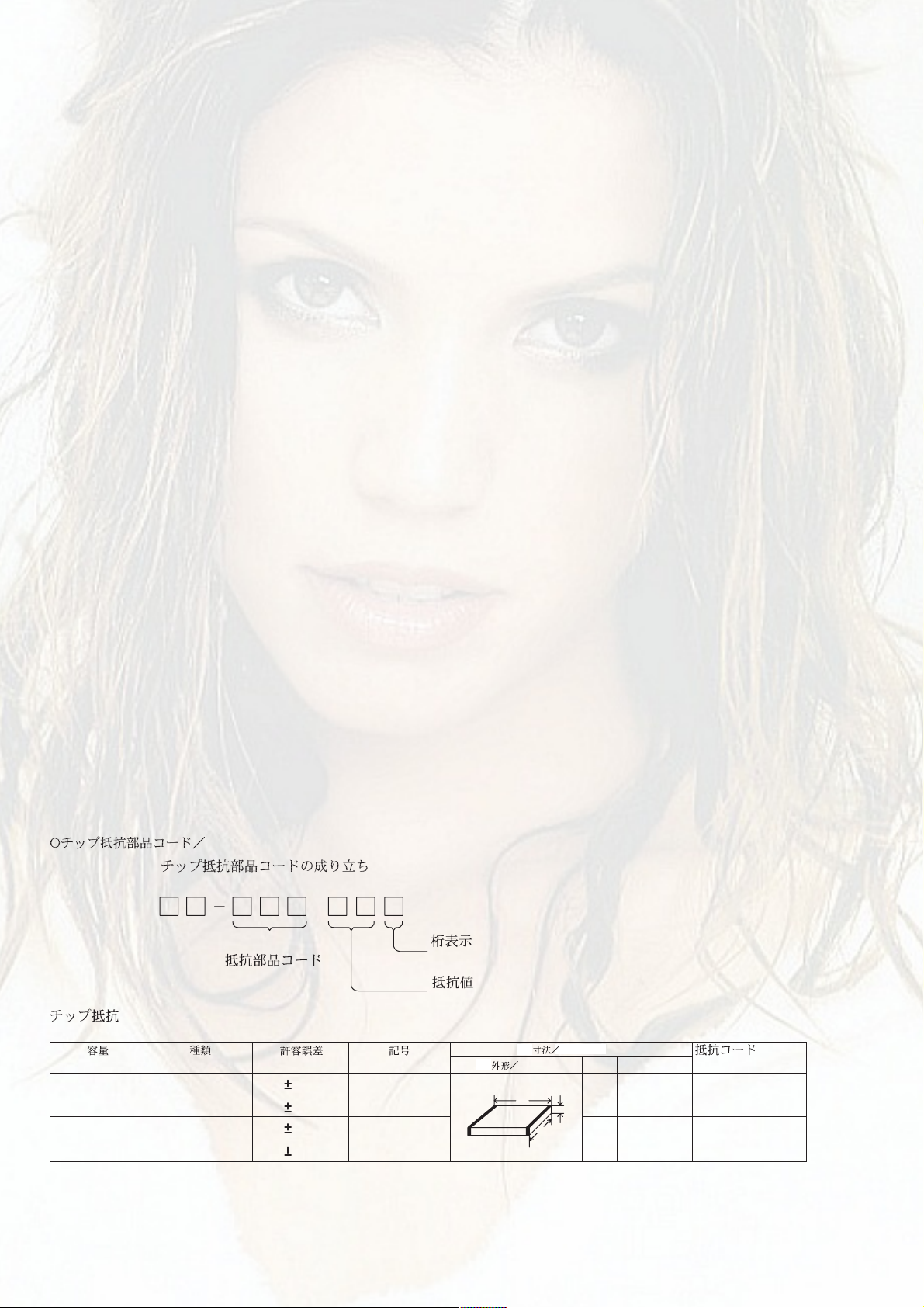
CHIP RESISTOR PART CODE
Chip Resistor Part Coding
88
A
Resistor Code
Chip resistor
Wattage Type Tolerance
1/16W 1005 5% CJ
1/16W
1/10W
1/8W
1608
2125
3216
5%
5%
5%
Symbol
CJ
CJ
CJ
Figure
Value of resistor
Form
L
17
Dimensions (mm)
t
W
0.55
Resistor Code
108
118
128
LW t
1.0 0.5 0.35 104
1.6 0.8 0.45
2 1.25 0.45
3.2
1.6
: A
: A
Page 18

TRANSISTOR ILLUSTRATION
E C B
2SA1296
CC5551
CSC4115
KTA1266
KTC3198
E C B
DTC114ES
KTC3199
B
2SA1235
2SA1369
2SC2714
2SC3326
CMBT5401
CMBT5551
CSD1306
E C B
CSD655
C
E
DTC114YKA
KRA102S
KRA107S
KRC102S
KTA1504
KTC3875
RT1P441C
B C E
2SB1370
G
S
2SK2158
B C E
2SB1677
2SD2619
D
D
S
G
2SK360
18
Page 19

WIRING – 1 (MAIN / HP – J)
32 31 30 29 28 27 26 25 24 23 22 21 20 19 18 17 16 15 14 13 12 11 10 9 8 7 6 5 4 3 2 1
A
B
C
D
E
F
G
H
I
J
K
L
M
N
O
P
Q
– 19 –
R
S
T
U
Page 20

SCHEMATIC DIAGRAM – 1 (MAIN : 1 / 2 / HP – J)
d u p a
t o r
– 20 –
Page 21

SCHEMATIC DIAGRAM – 2 (MAIN : 2 / 2 <MICON SECTION>)
d u p a
t o r
– 21 –
Page 22

WIRING – 2 (FRONT / AMP)
32 31 30 29 28 27 26 25 24 23 22 21 20 19 18 17 16 15 14 13 12 11 10 9 8 7 6 5 4 3 2 1
A
B
C
D
E
F
G
H
I
J
K
L
M
N
O
P
Q
d u
– 22 –
p a
t o r
R
S
T
U
Page 23

SCHEMATIC DIAGRAM – 3 (FRONT)
d u p a
t o r
– 23 –
Page 24

SCHEMATIC DIAGRAM – 4 (AMP)
d u p a
t o r
– 24 –
Page 25

WIRING – 3 (TUNER)
32 31 30 29 28 27 26 25 24 23 22 21 20 19 18 17 16 15 14 13 12 11 10 9 8 7 6 5 4 3 2 1
A
B
C
D
E
F
G
H
I
J
K
L
M
N
O
P
Q
d u
– 25 –
p a
t o r
R
S
T
U
Page 26

SCHEMATIC DIAGRAM – 5 (TUNER)
d u p a
t o r
– 26 –
Page 27

WIRING – 4 (AC 2M / PT MAIN)
32 31 30 29 28 27 26 25 24 23 22 21 20 19 18 17 16 15 14 13 12 11 10 9 8 7 6 5 4 3 2 1
A
B
C
D
E
F
G
H
I
J
K
L
M
N
O
P
Q
d u
– 27 –
p a
t o r
R
S
T
U
Page 28

SCHEMATIC DIAGRAM – 6 (AC 2M / PT MAIN)
d u p a
t o r
– 28 –
Page 29

WIRING 5 (CD) <1 / 2>
32 31 30 29 28 27 26 25 24 23 22 21 20 19 18 17 16 15 14 13 12 11 10 9 8 7 6 5 4 3 2 1
A
B
C
D
E
F
G
H
I
J
K
L
<WHT>
,,
M
N
O
P
Q
d u
29
p a
t o r
R
S
T
U
Page 30

WIRING 5 (CD) <2 / 2>
1 2 3 4 5 6 7 8 9 10 11 12 13 14 15 16 17 18 19 20 21 22 23 24 25 26 27 28 29 30 31 32
A
B
C
D
E
F
G
H
I
J
K
L
M
N
O
P
Q
R
S
T
U
d u
30
p a
t o r
Page 31

SCHEMATIC DIAGRAM – 7 (CD)
d u
– 31 –
p a
t o r
Page 32

FL (9 ST 24GONK) GRID ASSIGNMENT / ANODE CONNECTION / PIN CONNECTION
GRID ASSIGNMENT
d u
p a
t o
r
32
Page 33

ANODE CONNECTION
d u
p a
t o
r
33
Page 34

d u
p a
t o
r
34
Page 35

PIN CONNECTION
d u
p a
t o
r
35
Page 36

IC BLOCK DIAGRAM
d u
p a
t o
r
36
Page 37

d u
p a
t o
r
37
Page 38

d u
p a
t o
r
38
Page 39

IC DESCRIPTION
IC, LC876580W-5T99
Pin No. Pin Name I/O Description
1 O-MD/ARDY O MD communication clock permission. "L": Permit. (Not used)
2 O-CD/CLK O CD DSP clock output.
3 O-CD/CE O CD DSP latch output.
4 O-CD/SQCLK O CD SUBQ clock output.
5 O-CD/DATA O CD DSP data output.
6 O-M/CONT O Function IC control output.
7 O-TU/ON O Tuner power on output. "H": Power on.
8 O-QSUR O QSURROUND IC control output. "H": QSURROUND on. (Not used)
9 O-BBE/A O BBE control output A. (Not used)
d u
10 O-BBE/B O BBE control output B. (Not used)
11 RESET I Reset input.
12 I-HOLD I System hold detection input.
13 XT2 Not used.
14 VSS1 Ground.
15 CF1 I Crystal oscillator input for system clock (9.43MHz).
16 CF2 O Crystal oscillator output for system clock (9.43MHz).
17 VDD1 Power supply.
18 O-C.SHIFT O Micro-computer clock shift control output.
19 I-CD/SW I CD mechanism status detection input.
20 I-LEVEL I Level meter input.
p a
21 I-KEY1 I Key input 1.
22 I-KEY2 I Key input 2.
23 I-JOG I Rotary encoder pulse input.
24 O-PLL/CLK O Tuner PLL clock output.
25 I-RDS/SIG I Tuner RDS signal input. <EZ only>
26 O-PLL/DATA O Tuner PLL data output.
27 I-RDS/CLK I Tuner RDS clock input. <EZ only>
28 I-TM/BASE I Tuner PLL time base input.
29 I-RMC I Remote controller pulse input.
30 ~ 45 NC Not connected.
t o
46 VDD3 Power supply.
47 ~ 50 NC Not connected.
51 VP Connected to ground.
52 ~ 55 NC Not connected.
56 I-AM10K I AM 10kHz/9kHz switch. "H": 10kHz step. (Not used)
57 I-FMJPN I FM wide, AM stereo enable. "H": Japan. (Not used)
58 I-3BAND I 3 Band enable. "H": Enable, "L": Disable. (Connected to VDD through a resistor)
59 I-XTSEL I CD DSP clock switch. "L": 16MHz, "H": 33MHz. (Not used)
60 I-ECO-OFF I ECO mode initial setting. "H": Initial ECO mode off. (Not used)
61 I-QSUR-OFF I QSURROUND mode initial setting. "H": Initial QSURROUND mode off. (Not used)
62 I-RDS-SEL I RDS existence switch. "H": RDS exist. (Connected to VDD through a resistor) <EZ only>
r
39
Page 40

Pin No. Pin Name I/O Description
63 I-SURRSEL I
64 I-LPCSEL I LPC on/off switch. "L": On, "H": Off. (Connected to VDD through a resistor)
65 I-BBE1 I BBE initial setting. (Not used)
66 I-BBE2 I BBE initial setting. (Not used)
67 I-T-BASS1 I T-BASS initial setting. (Connected to VDD through a resistor)
68 I-T-BASS2 I T-BASS initial setting. (Not used)
69 ~ 71 NC Not connected.
72 VDD4 Power supply.
d u
73 I-MD/CLS I MD close detection input. (Not used)
74 O-TEST-CLK O Test clock output.
75 O-RVS O CD loading mechanism motor reverse output.
76 O-FWD O CD loading mechanism motor forward output.
77 I-CD/SUBQ I CD SUBQ data input.
78 I-CD/SENSE I CD SENS input.
79 O-CD/RW O CD-RW output.
80 O-CD/ON O CD power on output.
81 I-STEREO I Tuner stereo detection input.
QSURROUND, BBE existence switch. "L": Exist, "H": Not exist.
(Connected to VDD through a resistor)
82 I-TUNE/IFC I Tuner tune detection input.
83 I-RDS/DATA I Tuner RDS data input. <EZ only>
p a
84 O-PLL/CE O Tuner PLL latch output.
85 O-FL/OE O FL blink display output. "H": FL light off.
86 O-FL/LAT O FL command latch output.
87 O-POWER O Power on control output.
88 O-MUTE O System mute output.
89 VSS2 Ground.
90 VDD2 Power supply.
91 O-LMT O Line out mute output.
92 O-MD/SRST O MD micro-computer reset output. (Not used)
93 O-MD/SREQ O MD serial request output. (Not used)
t o
94 O-MD/REC O Not used.
95 O-FL/SI O FL serial data output.
96 O-MD/REQ O Not used.
97 O-FL/CLK O FL serial clock output.
98 O-MD/SIN O MD serial data output. (Not used)
99 I-MD/SOUT I MD serial data input. (Not used)
100 I-MD/ACLK I MD serial send permission input. "L": Permit. (Not used)
r
40
Page 41

IC, CXA1992AR
Pin No. Pin Name I/O Description
1 FEO O
2 FEI I Input terminal for focus error.
3 FDFCT I Capacitor connection terminal for time constant used when there is defect.
4 FGD I
5 FLB I
6 FE-O O Focus drive output.
d u
7 FE-M I Focus amplifier inverted input.
8 SRCH I
9 TGU I
10 TG2 I
11 FSET I Pin for setting peak of the phase compensator of the focus tracking.
12 TA-M I Tracking amplifier inverted input.
Output terminal for focus error amplifier. Internally connected to window comparator input for
bias condition.
This pin is connected to GND via capacitor when high frequency gain of the focus servo is
attenuated.
This is a pin where the time constant is externally connected to raise the low frequency gain of the
focus servo.
This is a pin where the time constant is externally connected to generate the focus search
waveform.
This is a pin where the selection time constant is externally connected to set the tracking servo the
high frequency gain.
This is a pin where the selection time constant is externally connected to set the tracking high
frequency gain.
13 TA-O O Tracking drive output.
14 SL-P I Sled amplifier non-inverted input.
p a
15 SL-M I Sled amplifier inverted input.
16 SL-O O Sled drive output.
17 ISET I
18 VCC I Power supply.
19 LOCK I L setting starts sled disorder-prevention circuit. (No pull-up resistance) (Connected to VC)
20 CLK I Clock input for serial data transfer from CPU. (No pull-up resistance)
21 XLT I Latch input from CPU. (No pull-up resistance)
22 DATA I Serial data input from CPU. (No pull-up resistance)
23 XRST I Reset system at L setting. (No pull-up resistance)
t o
24 C-OUT O Signal output for track number counting.
25 SENS1 O
26 SENS2 O DFCT2, MIRR, BALL, TGL or FOL is output depending on the command from CPU.
27 FOK O Output terminal for focus OK comparator.
28 CC2 I Input pin where the DEFECT bottom hold output is capacitance coupled.
The current which determines height of the focus search, track jump and sled kick is input with
external resistance connected.
FZC, DFCT1, TZC, BALH, TGH, FOH, or ATSC is output depending on the command from
CPU.
29 CC1 O DEFECT bottom-hold output terminal. Internally connected to interruption comparator input.
30 CB I Connection terminal for DEFECT bottom-hold capacitor.
31 CP I Connection terminal for MIRR hold-capacitor. Anti-reverse input terminal for MIRR comparator.
32 RF-I I Input terminal by capacity combination of RF summing amplifier.
33 RF-O O Output terminal of RF summing amplifier. Checkpoint of Eye pattern.
r
41
Page 42

Pin No. Pin Name I/O Description
34 RF-M I
35 RFTC I This is a pin where the selection time constant is externally connected to control the RF level.
36 LD O APC amplifier output terminal.
37 PD I APC amplifier input terminal.
38 ~ 39 PD1 ~ PD2 I
40 FE I/O Bias adjustment pin of the focus error amplifier. (Not used)
41 ~ 42 F ~ E I
d u
43 EI
44 VEE GND connection pin.
45 TEO O Output terminal for tacking-error amplifier. Output E-F signal.
46 LPFI I BAL adjustment comparator input pin. (Input through LPF from TEO)
47 TEI I Input terminal for tracking error.
48 ATSC I Window-comparator input terminal for detecting ATSC.
49 TZC I Input terminal for tracking-zero cross comparator.
Anti-reverse input terminal for RF summing amplifier. The gain of RF amplifier is decided by the
connection resistance between RF-M and RF-O terminals.
RFI-V amplifier inverted input pin. These pins are connected to the A+C and B+C pins of the
optical pickup, receiving by currents input.
F and EIV amplifier inverted input pins. These pins are connected to the F and E of the optical
pickup, receiving by current input.
Gain adjustment pin of the I-V amplifier E. (When not in use of BAL automatic adjustment)
(Not used)
50 TDFCT I Capacitor connection pin for the time constant used when there is defect.
51 VC O Output terminal for DC voltage reduced to half of VCC+VEE.
p a
52 FZC I Input terminal for focus-zero cross comparator.
IC, CXD2589Q
Pin No. Pin Name I/O Description
1 VSS GND.
2 LMUT O Left channel zero detection flag. (Not used)
3 RMUT O Right channel zero detection flag. (Not used)
4 SQCK I SQSO readout clock input.
t o
5 SQSO O Sub Q 80-bit serial output.
6 SENSE O SENS output to CPU.
7 DATA I Serial data input from CPU.
8 XLAT I Latch input from CPU. Serial data is latched at the falling edge.
9 XCLK I Serial data transfer clock input from CPU.
10 SEIN I SENS input from SSP.
11 CNIN I Track jump count signal input.
12 DATO I Serial data output to SSP.
13 XLTO O Serial data latch output to SSP. Latched at the falling edge.
14 CLKO O Serial data transfer clock output to SSP.
15 SPOA(SENS2) I Microcomputer extended interface (input A). (SENS input from SSP.)
r
42
Page 43

Pin No. Pin Name I/O Description
16 SPOB(IN/SW) I Microcomputer extended interface (input B). (CD pickup inside limit switch.)
17 XLON O Microcomputer extended interface (output). (Not used)
18 FOK I Focus OK input. Used for SENS output and the servo auto sequencer.
19 VDD Power supply (+5V).
20 VSS GND.
21 MDP O Spindle motor servo control.
22 PWMI I Spindle motor external control input. (Not used)
23 ~ 24 TEST I TEST pin. (Connected to GND)
25 VPCO O Charge pump output for the wide-band EFM PLL. (Connected to GND)
d u
26 VCKI I VCO2 oscillation input for the wide-band EFM PLL.
27 V16M O VCO2 oscillation output for the wide-band EFM PLL.
28 VCTL I VCO2 control voltage input for the wide-band EFM PLL. (Connected to GND)
29 PCO O Master PLL charge pump output.
30 FILO O Master PLL (slave = digital PLL) filter output.
31 FILI I Master PLL filter input.
32 AVSS Analog GND.
33 CLTV I Master VCO control voltage input.
34 AVDD Analog power supply (+5V).
35 RF I EFM signal input.
36 BIAS I Constant current input of the asymmetry circuit.
p a
37 ASYI I Asymmetry comparator voltage input.
38 ASYO O EFM full swing output. "L" = VSS, "H" = VDD.
39 LRCK O D/A interface. LR clock output f = Fs.
40 LRCKI I LR clock input.
41 PCMD O D/A interface. Serial data output (two's complement, MSB first).
42 PCMDI I D/A interface. Serial data input (two's complement, MSB first).
43 BCK O D/A interface. Bit clock output.
44 BCKI I D/A interface. Bit clock input.
45 VSS GND.
46 VDD Power supply (+5V).
t o
47 XUGF O XUGF output. Switched to MNT1 or RFCK output by a command. (Not used)
48 XPCK O XPCLK output. Switched to MNT0 output by a command. (Not used)
49 GFS O GFS output. Switched to MNT3 or XRAOF output by a command. (Not used)
50 C2PO O C2PO output. Switched to GTOP output by a command. (Not used)
51 XTSL I Crystal selector input. "L" = 16.9344MHz, "H" = 33.8688MHz. (Connected to GND)
52 C4M O 4.2336MHz output. 1/4 frequency divided VCKI output in CAV-W mode. (Not used)
53 DOUT O Digital out output.
54 EMPHO O
55 EMPHI I Inputs a high signal when de-emphasis is on, and a low signal when de-emphasis is off.
56 WFCK O WFCK output. (Not used)
Outputs a high signal when the playback disc has emphasis, and a low signal when there is no
emphasis.
r
43
Page 44

Pin No. Pin Name I/O Description
57 SCOR O Outputs a high signal when either subcode sync S0 or S1 is deteected. (Not used)
58 SBSO O Sub P to W serial output. (Not used)
59 EXCK I SBSO readout clock input. (Connected to GND)
60 VSS GND.
61 VDD Power supply (+5V).
62 SYSM I Mute input. Active when high. (Connected to GND)
63 AVSS Analog GND.
64 AVDD Analog power supply (+5V).
65 AOUT1 O Left channel analog output.
d u
66 AIN1 I Left channel operational amplifier input.
67 LOUT1 O Left channel LINE output.
68 AVSS Analog GND.
69 XVDD Power supply for master clock.
70 XTAI I Crystal oscillation circuit input. Input the external master clock via this pin.
71 XTAO O Crystal oscillation circuit output.
72 XVSS GND for master clock.
73 AVSS Analog GND.
74 LOUT2 O Right channel LINE output.
75 AIN2 I Right channel operational amplifier input.
76 AOUT2 O Right channel analog output.
p a
77 AVDD Analog power supply (+5V).
78 AVSS Analog GND.
79 XRST I System reset. Reset when low.
80 VDD Power supply (+5V).
Notes: PCMD is an MSB first, two's complement output.
GTOP is used to monitor the frame sync protection status. (High: sync protection window open.)
XUGF is the negative pulse for the frame sync obtained from the EFM signal. It is the signal before sync protection.
XPLCK is the inverse of the EFM PLL clock. The PLL is designed so that the falling edge of XPCLK and the EFM signal transition point
coincide.
GFS goes high when the frame sync and the insertion protection timing match.
RFCK is derived from the crystal accuracy, and has a cycle of 136µ (during normal speed).
t o
C2PO represents the data error status.
XRAOF is generated when the 16K RAM exceeds the ±48F jitter margin.
r
44
Page 45

IC, LC72131D-N
Pin No. Pin Name I/O Description
1 X-IN I
22 X-OUT O
2 NC Not connected.
3 CE I To enable the IC. Active "H".
A crystal oscillator (4.5MHz) is connected between these pins.
4DII
5 CL I To clock in the data DI.
6 DO O Digital data output to CPU (LC876580W-5T99).
7 T-BASE O Outputs a reference clock signal (8Hz) for the clock.
d u
8 MONO / BEAT O Outputs "H" when MONO / BEAT is switched.
9 FM / SW O
10 MW / SW O
11 IF-MUTE O To control internal counter.
12 IF-IN I General purpose counter input.
p a
13 TUNE I Receives "L" when station is tuned.
14 NC Not connected.
Digital data input from CPU (LC876580W-5T99) when relevant key is operated.
Active "H".
Output "L" or "H" as follows:
2 BAND 3 BAND 3 BAND
AM FM LW MW FM MW SW FM
HLHHLHLL
Outputs "L" or "H" as follows:
2 BAND 3 BAND 3 BAND
AM FM LW MW FM MW SW FM
LLHLLLHL
15 AM-IN I Receives the AM local oscillator frequency signal.
16 FM-IN I Receives the FM local oscillator frequency signal.
17 VDD Supply power to IC (+5V).
18 PD O PLL charge pump output.
19 A-IN I
20 A-OUT O
21 VSS Ground.
The MOS transistor used for PLL active low pass filter.
t o
r
45
Page 46

ADJUSTMENT (TUNER / MICON)
< TUNER SECTION >
1. Clock Frequency Check
Settings : Test point : TP2 (CLK)
Method : Set to MW 1602kHz and check that the test point is
2052kHz ± 45Hz.
2. MW VT Check
Settings : Test point : TP1 (VT)
Method : Set to MW 1602kHz and check that the test point is
less than 8.0V. Then set to MW 531kHz and check
that the test point is more than 0.6V.
3. MW Tracking Adjustment
Settings : Test point : TP8 (Rch), TP9 (Lch)
Adjustment location : L951 (1/3)
Method : Set to MW 999kHz and adjust L951 (1/3) so that the
test point becomes maximum.
d u
4. LW VT Adjustment
Settings : Test point : TP1 (VT)
Adjustment location : L942
Method : Set to LW 144kHz and adjust L942 so that the test
point becomes 1.3V ± 0.05V. Then set to LW 290kHz
and check that the test point is less than 8.0V.
8. FM Tracking Adjustment
Settings : Test point : TP8 (Rch), TP9 (Lch)
Adjustment location : L901, L902, L904, L905
Method : Set to FM 108.0MHz and adjust L901, L902, L904,
L905 so that the waveform at the test point becomes
maximum with minimum distortion. Then set to
FM 98.0MHz and check that the test point is less than
13dBµV.
9. DC Balance / Mono Distortion Adjustment
Settings : Test point : TP3, TP4 (DC)
Adjustment location : L801
Input level : 60dBµV
Method : Set to FM 98.0MHz and adjust L801 so that the
voltage between TP3 and TP4 becomes 0V ± 500mV
with distortion less than 1.2%.
10. Output Level Check
<MW>
Settings : Test point : TP8 (Rch), TP9 (Lch)
Input level : 74dBµV
Method : Set to MW 999kHz and check that the test point is
55mV ± 3dB.
5. LW Tracking Adjustment
Settings : Test point : TP8 (Rch), TP9 (Lch)
Adjustment location :
L941 .................................................... 144kHz
TC942 .................................................. 290kHz
Method : Set up TC942 to center before adjustment.
The level at 144kHz is adjsuted to MAX. by L941.
Then the level at 290kHz is adjusted to MAX. by
TC942.
p a
6. AM IF Adjustment
Settings : Test point : TP8 (Rch), TP9 (Lch)
Adjustment location :
L802 .................................................... 450kHz
7. FM VT Adjustment
Settings : Test point : TP1 (VT)
Adjustment location : L907
Method : Set to FM 108.0MHz and adjust L907 so that
the test point becomes 7.0V ± 0.05V. Then set
to FM 87.5MHz and check that the test point is
more than 0.5V.
t o
<FM>
Settings : Test point : TP8 (Rch), TP9 (Lch)
Input level : 60dBµV
Method : Set to FM 98.0MHz and check that the test point is
270mV ± 3dB.
11. FM Separation Check
Settings : Test point : TP8 (Rch), TP9 (Lch)
Input level : 60dBµV
Method : Set to FM 98.0MHz and check that the test point is
more than 12dB.
<MICON SECTION >
12. µ-CON OSC Adjustment
Settings : Test point : TP1 (TP), GND
Adjustment location : L101
Method : Insert AC plug while pressing of "DISPLAY" key.
Connect a frequency counter across TP1 and GND.
Then adjust L101 so that the test point becomes
98.09Hz ± 0.098Hz.
r
46
Page 47

CD TEST MODE
1. How to Start the CD Test Mode
While pressing the ENTER key, connect the AC power plug to the wall outlet.
When the test mode starts up, all indicators light.
2. How to Exit the CD Test Mode
Either press the POWER button or press any button other than CD or disconnect the AC power plug.
* If a disc has not been inserted, the CD test mode does not function.
3. Function Descriptions and Use of the CD Test Mode
No
1
2
3
4
5
Mode
Start mode
Search
d u
mode
Play mode
Traverse
p a
mode
Sled mode
Operation
STOP
button
Play button
PAUSE
button
FF button
REW button
FL Display
All indicators light
TOC reading
Normal time
display
Normal time
display
CD TEST
CD TEST
Function
LD emits laser light.
Continuous focus search
operation. *1
Normal playback.
When TOC reading is not
possible, search mode of item
2 is repeated.
OFF/ON repeats whenever
the tracking servo ON/OFF is
pressed.
Optical pickup moves to the
outer circumference. *2
Optical pickup moves to the
inner circumference. (Normal
operation during PLAY mode.)
Checking item
FL check
Microprocessor check
APC circuit check
Laser current measurement
Focus search waveform check
Focus error waveform check
(FOK in the search mode/FZC
is not monitored.)
Focus servo
Tracking servo
Sled servo
Spindle servo
FOK
RF waveform
Tracking servo
Traverse waveform
Sled circuit
Mechanism
*1: If the focus search continues for 10 minutes or longer, the driver IC heats up and the protection circuit starts working.
Because of this, there can be a case that a machine does not work at all. In such a case, turn off the main power once.
After it is cooled down, restart the machine.
*2: If the FF button or the RWD button is kept pressed, the gear can be damaged because the sled motor keeps rotating even
3-1. Outline of Operation
t o
after the optical pickup has reached the innermost circumference or the outermost circumference.
When the respective buttons are pressed in the start mode, operation mode changes in the direction of the arrow so that the
respective test modes can be used.
Start mode
All indicators light
Search mode Traverse mode
Play mode
r
47
Page 48

4. TRAY (Loading Mechanism) Test Mode
When the TUNER/BAND key is pressed while all indicators light in the CD test mode, the display as shown appears.
Pressing the TUNER/BAND key again returns to the CD test mode.
4-1. TRAY Test Mode Operations and Displays
Pressing the FF key rotates the motor (F display) in the loading direction.
Pressing the REW key rotates the motor (R display) in the unloading direction.
d u
Loading Unloading
4-2. Detection Switch Display
When a disc is inserted and the FF/REW key is pressed, ON/OFF operation of the detection switch can be checked.
Switch No. Detection contents Detection method
1 DISC IN switch Disc insertion is detected at L.
p a
2 12 cm/8 cm disc is detected 8 cm disc is detected when switch No. 2 is L and No. 3 is H.
3 (during loading) 12 cm disc is deteded when switch No. 2, 3 is L.
4 Loading end switch Goes H at the chucking completed state.
t o
Detection switch display
r
48
Page 49

MECHANICAL PARTS ARRANGEMENT 1 / 5
d u
49
p a
t o r
Page 50

MECHANICAL PARTS ARRANGEMENT 2 / 5
d u
50
p a
t o r
Page 51

MECHANICAL PARTS ARRANGEMENT 3 / 5
d u
51
p a
t o r
Page 52

MECHANICAL PARTS ARRANGEMENT 4 / 5
d u
52
p a
t o r
Page 53

MECHANICAL PARTS ARRANGEMENT 5 / 5
d u
53
p a
t o r
Page 54

MECHANICAL PARTS LIST 1 / 1
PART NO. DESCRIPTIONREF. NO. KANRI
1 8B-CL5-048-010 PANEL,SIDE R(B)
2 8B-CL5-047-010 PANEL,SIDE L(B)
3 8B-CL5-046-010 CABI,TOP(B)
4 8B-CL5-201-010 HLDR,FR
5 8B-CL5-005-010 CABI,REAR EZ
6 8B-CL5-616-010 FAN,F410T-12L1C-01-140MM
7 8A-CJ5-209-010 GUIDE,FL
8 8B-CJ5-205-010 HLDR,CD B
!
9 8B-CL5-613-010 PT,EZK 57-35-BCL5
10 8B-CL5-607-010 FF-CABLE,10P 1.0 120MM
11 8B-CL5-609-010 CONN ASSY,2P SHLD 250MM
12 8B-CJ5-208-010 HLDR,TR A
13 8B-CL5-203-010 COVER,CD
14 8A-CJ5-204-010 HLDR,ECO
15 8B-CL5-042-010 SH,FRONT-J EZ
16 8B-CJ5-209-010 HLDR,TR B
17 8B-CJ5-210-010 HLDR,JACK HP
!
18 87-A80-157-010 AC CORD ASSY,E BLK CC
19 87-085-185-010 BUSHING,AC CORD(E) CM-22B
20 8B-CL5-037-010 KNOB,RTRY JOG(B)
21 8B-CJ5-211-010 HLDR,KEY
22 8Z-KM1-220-010 MAGNET,HLDR ASSY
23 8B-CL5-031-010 KEY,POWER(B)
24 8B-CJ5-018-010 REFLECTOR,POWER
25 8B-CL5-034-010 KEY,ENTER(B)
26 8B-CL5-035-010 KEY,REC(B)
27 8B-CL5-033-010 KEY,SKIP(B)
28 8B-CL5-032-010 KEY,PLAY(B)
29 8B-CL5-039-010 KEY ASSY,EJECT CD(B)
30 8B-CJ5-217-010 SPR-P,HINGE
d u
NO.
DESCRIPTIONREF. NO. KANRI
PART NO.
31 8B-CL5-049-010 DUST COVER, CD LMS
32 8B-CL5-044-010 CABI,FR(B) EZ<EZ>
32 8B-CL5-045-010 CABI,FR(B) K<K>
33 8B-CJ5-028-010 GUIDE,DOOR
34 8B-CJ5-215-010 GUIDE,HINGE T
35 8B-CJ5-216-010 GUIDE,HINGE B
36 8B-CJ5-214-010 GEAR,DOOR
37 8B-CL5-043-010 HLDR,HINGE(B)
38 8B-CL5-013-010 WINDOW,DOOR<K>
38 8B-CL5-020-010 WINDOW,DOOR EZ<EZ>
39 8B-CJ5-020-010 HLDR,DOOR
40 8B-CJ5-212-010 PLATE,MAGNET
!
41 87-099-811-010 PLUG,ADPTR CONV(K)<K>
A 87-067-641-010 UTT2+3-8 W/O SLOT BLK
B 87-067-579-010 BVT2+3-8 W/0 SL0T
C 87-721-096-410 QT2+3-10 W/O SLOT
D 87-067-660-010 BVT2+3-8 W/0 SL0T BLK
E 87-751-098-410 VT2+3-14 W/O SLOT
F 87-591-094-410 QIT+3-6
G 87-067-688-010 BVTT+3-6
H 87-B10-316-010 BVIT3B+3-10 R W/O
I 87-B10-314-010 BVIT3B+3-6 R W/O
J 87-B10-315-010 BVIT3B+3-8 R W/O
K 87-078-200-010 S-SCREW,ITC+4-8 R
L 87-067-703-010 BVT2+3-10 W/0 SL0T
M 87-067-868-010 V+1.7-4 BLK HL
N 87-067-384-010 VT2+1.4-3.5 SWCH HL
O 87-067-359-010 S-SCREW,+1.4-2.5 CR BLK
P 87-NF4-224-010 S-SCREW,IT3B+3-8 CU
NO.
p a
COLOR NAME TABLE
Basic color symbol Color Basic color symbol Color Basic color symbol Color
B Black C Cream D Orange
G Green H Gray L Blue
LT Transparent Blue N Gold P Pink
R Red S Silver ST Titan Silver
T Brown V Violet W White
WT Transparent White Y Yellow YT Transparent Yellow
t o
LM Metallic Blue LL Light Blue GT Transparent Green
LD Dark Blue DT Transparent Orange GM Metallic Green
YM Metallic Yellow DM Metallic Orange PT Transparent Pink
LA Aqua Blue GL Light Green HT Transparent Gray
r
54
Page 55

CD MECHANISM EXPLODED VIEW 1 / 1
19
22
18
42
17
5
A
3
B
4
13
12
11
16
8
15
45
22
6
7
23
46
9
10
24
21
29
5
A
6
7
14
2
25
26
27
A
28
30
31
9
C
2
a
b
1
PWB
44
2
43
35
38
b
a
41
39
20
A
40
37
D
E
36
32
33
A
34
A
d u
55
p a
t o r
Page 56

CD MECHANISM PARTS LIST 1 / 1
PART NO. DESCRIPTIONREF. NO. KANRI
1 8A-ZGA-243-110 HLDR,MECHA
2 8A-ZGA-267-010 CUSH,MECHA
3 8A-ZGA-204-110 GUIDE,CD FR
4 8A-ZGA-202-110 PLATE,CD FR
5 8A-ZGA-232-010 SPR-P,GUIDE
6 8A-ZGA-247-010 ROLLER,LVR CD
7 8A-ZGA-246-010 SHAFT,LVR CD
8 8A-ZGA-253-010 SPR-E,LVR CD
9 8A-ZGA-266-010 DMPR,CD
10 8A-ZGA-255-010 SPR-E,MECHA
11 8A-ZGA-251-010 SPR-T,ROLLER R
12 8A-ZGA-250-010 SPR-T,ROLLER L
13 8A-ZGA-216-110 LEVER ASSY,ROLLER
14 8A-ZGA-206-010 LEVER,CD L
15 8A-ZGA-207-010 LEVER,CD R
16 8A-ZGA-261-010 ROLLER,RUBBER
17 8A-ZGA-214-010 CAP,DISC
18 8A-ZGA-211-010 HLDR ASSY,CLAMP
19 8A-ZGA-215-010 PLATE,DISC
20 8A-ZGA-234-010 PLATE,LVR LINK
21 8A-ZGA-222-010 GEAR,ROLLER
22 8A-ZGA-220-010 CLR,ROLLER
23 8A-ZGA-262-010 BELT,LOAD
24 8A-ZGA-225-010 GEAR,PULLEY
25 8A-ZGA-257-010 SPR-T,TRIG
26 8A-ZGA-254-010 SPR-E,LVR TRIG
27 8A-ZGA-209-010 LEVER,TRIG
28 8A-ZGA-203-010 PLATE,CD RE
29 8A-ZGA-236-010 LEVER ASSY,8CD
30 8A-ZGA-256-010 SPR-E,LVR 8CD
d u
NO.
DESCRIPTIONREF. NO. KANRI
PART NO.
NO.
31 8A-ZGA-208-010 LEVER,LOAD
32 8A-ZGA-205-010 GUIDE,CD RE
33 8A-ZGA-223-110 PLATE,SLIDER
34 8A-ZGA-252-010 SPR-E,SLIDE
35 8A-ZGA-226-010 GEAR,REDUCTION
36 8A-ZGA-229-010 ARM ASSY,GEAR
37 8A-ZGA-228-010 GEAR,IDLER
38 8A-ZGA-227-010 GEAR,SLIDER
39 87-A91-914-010 MOT,M25E-10
40 8A-ZGA-224-010 PULLEY,MOT
41 8A-ZGA-240-010 SHAFT,BASE
42 8A-ZGA-219-110 SHAFT,ROLLER
43 8A-ZGA-201-110 BASE
44 M8-AZK-S90-000 KSM-900AMA
45 8A-ZGA-265-010 SH, 4.5-2.1-0.25 W/O ADH
46 8A-ZGA-260-010 SH, 6-2.55-0.5 W/ADH
A 88-ZG5-302-010 S-SCREW,8ZG5+2-4 W/O
B 8A-ZGA-272-010 S-SCREW,CD MECHA
C 87-262-527-310 SCREW, V+1.7-3
D 88-ZG5-303-010 VFT2+2-8 W/O
E 8A-ZGA-274-010 VFT2+2-16 W/O
p a
t o
r
56
Page 57

GENERAL SPEAKER DISASSEMBLY INSTRUCTIONS (FOR REFERENCE)
Type.1
Insert a flat-bladed screwdriver into the position indicated by the
arrows and remove the panel. Remove the screws of each speaker
unit and then remove the speaker units.
d u
Type.2
Remove the grill frame and four pieces of rubber caps by pulling
out with a flat-bladed screwdriver. Remove the screws from hole
where installed rubber caps. Insert a flat-bladed screwdriver into
the position indicated by the arrows and remove the panel. Remove the screws of each speaker unit and then remove the speaker
units.
Type.4
TOOLS
1 Plastic head hammer
2 (() flat head screwdriver
3 Cut chisel
12 3
How to Remove the PANEL, FR
1. Insert the (() flat head screwdriver tip into the gap
between the PANEL, FR and the PANEL, SPKR. Tap the
head of the (() flat head screwdriver with the plastic
hammer head, and create the clearance as shown in Fig-1.
2. Insert the cut chisel in the clearance, and tap the head of
the cut chisel with plastic hammer as shown in Fig-2, to
remove the PANEL, FR.
p a
Type.3
Insert a flat-bladed screwdriver into the position indicated by the
arrows and remove the panel. Turn the speaker unit to counterclockwise direction while inserting a flat-bladed screwdriver into
one of the hollows around speaker unit, and then remove the speaker
unit. After replacing the speaker unit, install it turning to clockwise
direction until "click" sound comes out.
t o
3. Place the speaker horizontally. Tap head of the cut chisel
with plastic hammer as shown in Fig-3, and remove the
PANEL, FR completely.
Fig-1 Fig-2
r
– 57 –
Fig-3
How to Attach the PANEL, FR
Attach the PANEL, FR to the PANEL, SPKR. Tap the four
corners of the PANEL, FR with the plastic hammer to fit the
PANEL, FR into the PANEL, SPKR completely.
Page 58

SPEAKER PARTS LIST (SX LMS5) <YJ1BN>
PART NO.
NO.
1 8B-CP5-001-010 PANEL,FR
2 8B-CP5-005-010 PANEL,TW
3 8B-CP5-003-010 GRILLE,FRAME ASSY
4 8A-CJ5-411-010 SPKR,W 87S
5 8A-CJ5-417-010 SPKR,TW 25
6 8B-CP5-610-010 CORD,SPKR
7 8A-CJ5-415-010 TERMINAL
DESCRIPTIONREF. NO. KANRI
d u
ACCESSORIES / PACKAGE LIST
PART NO.
1 8B-CL5-905-010 IB,K(E)M<K>
1 8B-CL5-906-010 IB,EZ(9L)M<EZ>
2 87-006-226-010 ANT,LOOP AM
3 87-A90-118-010 ANT,WIRE FM(Z)
4 8B-CL5-951-010 RC UNIT,RC-BAT01
!
5 87-099-811-010 PLUG,ADPTR CONV(K)<K>
NO.
DESCRIPTIONREF. NO. KANRI
p a
t o
r
58
Page 59

d u
p a
t o
r
211, IKENOHATA 1CHOME, TAITO-KU, TOKYO 110, JAPAN TEL:03 (3827) 3111
Printed in Singapore9420025 2000045 921338 931261
 Loading...