

Page 1
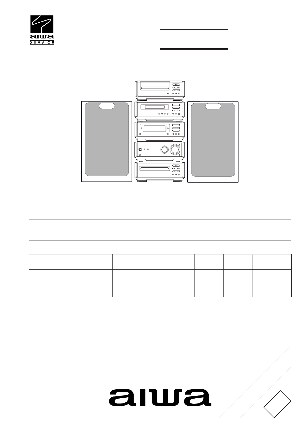
XR-M918
K
XR-M919
EZ
SERVICE MANUAL
COMPACT DISC STEREO SYSTEM BASIC CD MECHANISM : 3ZG-3 E13NM
SYSTEM
XR-M918
XR-M919
STEREO
TUNER
TX-LM918
TX-LM919 MX-LM919
• This Service Manual is the “Revision Publishing” and replaces “Simple Manual”
XR-M919 (EZ), (S/M Code No. 09-014-444-6T1) and
XR-M918 (K), (S/M Code No. 09-014-444-6T2).
• If requiring information about FX-LM918, see Service Manual of FX-LM918 (Y),
(S/M Code No. 09-015-444-7R1).
STEREO
INTEGRATED
AMPLIFIER
MX-LM918
COMPACT
DISC PLAYER
DX-LM918
STEREO
CASSETTE
DECK
FX-LM918
(OPTIONAL)
MINI DISC
RECORDER
AM-LM918
(OPTIONAL)
SPEAKER
SX-LM918
REMOTE
CONTROLLER
RC-BAT02
• If requiring information about AM-LM918, see Service Manual of AM-LM918 (Y),
(S/M Code No. 09-016-446-9R1).
REVISION
S/M Code No. 09-017-444-6R1
DATA
Page 2

TABLE OF CONTENTS
SPECIFICATIONS ...............................................................................................................................................................3
PROTECTION OF EYES FROM LASER BEAM DURING SERVICING ......................................................................4
MODEL NO. TX–LM918 / LM919
ELECTRICAL MAIN PARTS LIST .............................................................................................................................. 5 ~ 7
TRANSISTOR ILLUSTRATION ..........................................................................................................................................8
WIRING – 1 (MAIN) <EZ>...................................................................................................................................................9
WIRING – 2 (MAIN) <K>................................................................................................................................................... 10
WIRING – 3 (FRONT / CONN / AUX / TAPE – JACK / LED – L / LED – R / LCD – LED) <EZ>...................................... 11
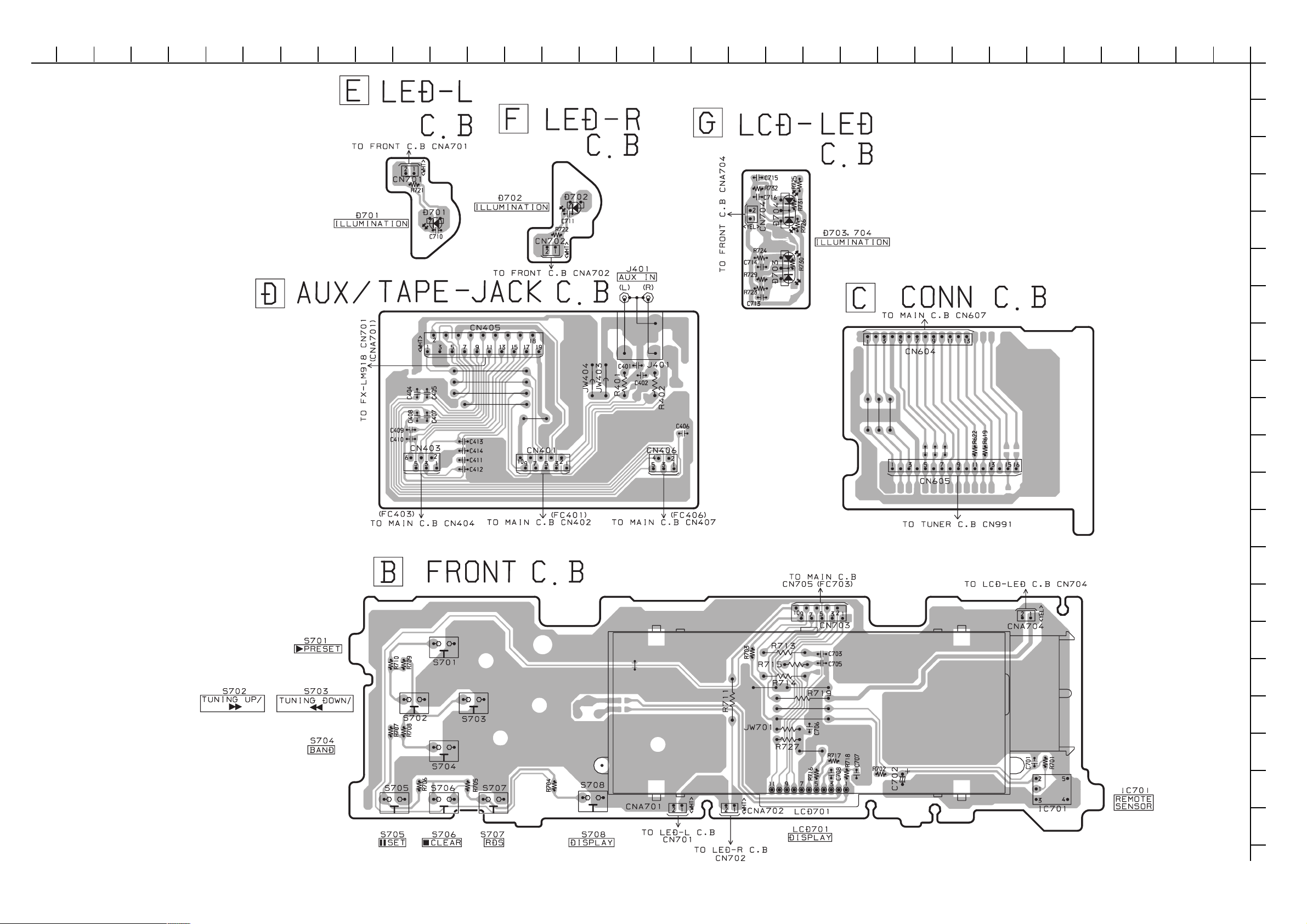
WIRING – 4 (FRONT / CONN / AUX / TAPE – JACK / LED – L / LED – R / LCD – LED) <K>........................................ 12
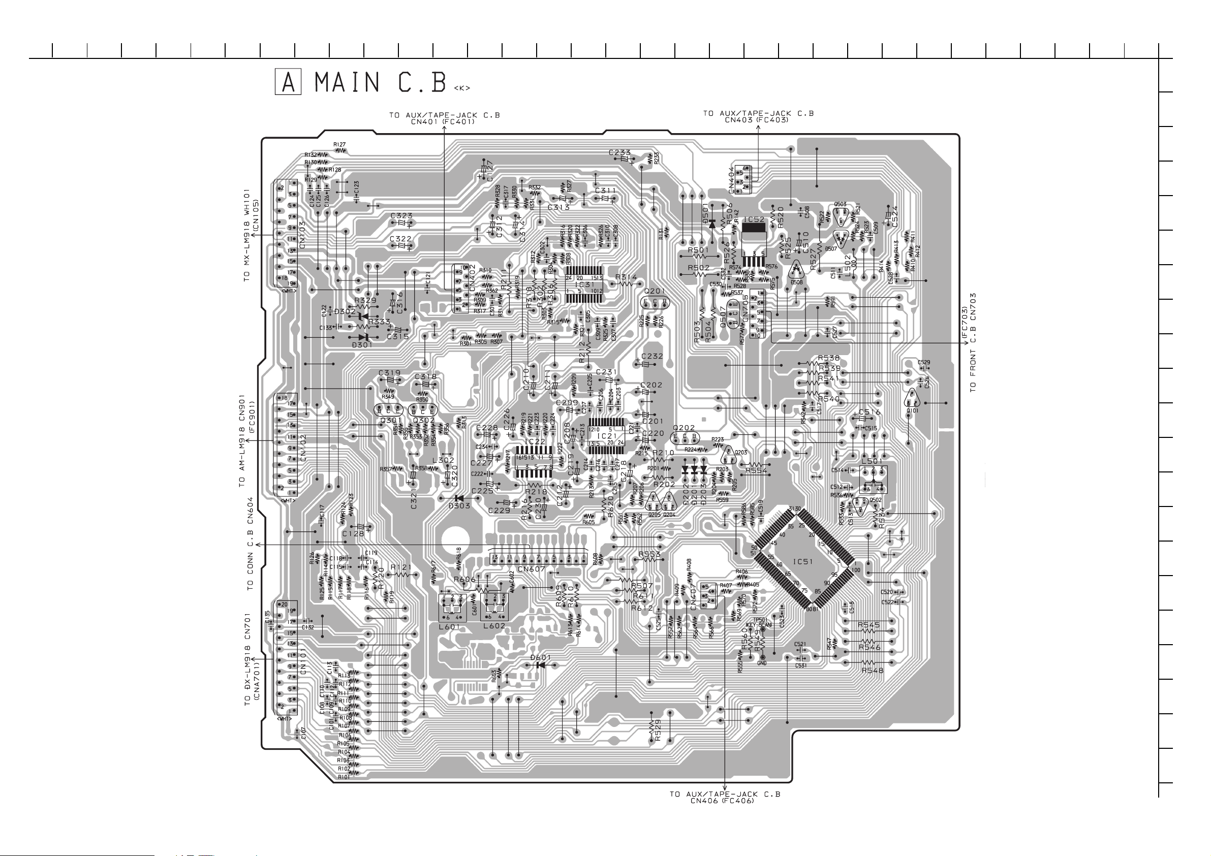
SCHEMATIC DIAGRAM – 1 (MAIN / FRONT / CONN / AUX / TAPE – JACK / LED – L / LED – R / LCD – LED) .......... 13
WIRING – 5 (TUNER) ........................................................................................................................................................ 14
SCHEMATIC DIAGRAM – 2 (TUNER) ............................................................................................................................. 15
IC BLOCK DIAGRAM.......................................................................................................................................................16
LCD DIAGRAM .................................................................................................................................................................17
IC DESCRIPTION ....................................................................................................................................................... 18, 19
ADJUSTMENT ................................................................................................................................................................... 20
MECHANICAL EXPLODED VIEW 1 / 1 <EZ> ............................................................................................................... 21
MECHANICAL PARTS LIST 1 / 1 <EZ> .........................................................................................................................22
MECHANICAL EXPLODED VIEW 1 / 1 <K> ................................................................................................................. 23
MECHANICAL PARTS LIST 1 / 1 <K> ........................................................................................................................... 24
MODEL NO. MX–LM918 / LM919
ELECTRICAL MAIN PARTS LIST ............................................................................................................................ 25, 26
TRANSISTOR ILLUSTRATION ........................................................................................................................................27
WIRING – 1 (PWB – AMP / HP) ........................................................................................................................................ 28
WIRING – 2 (SPK / FRONT / LED – L / LED – R / AC) .....................................................................................................29
SCHEMATIC DIAGRAM (PWB – AMP / SPK / FRONT / HP / LED – L / LED – R / AC).................................................. 30
MECHANICAL EXPLODED VIEW 1 / 1 <EZ> ................................................................................................................ 31
MECHANICAL PARTS LIST 1 / 1 <EZ> .........................................................................................................................32
MECHANICAL EXPLODED VIEW 1 / 1 <K> ..................................................................................................................33
MECHANICAL PARTS LIST 1 / 1 <K> ........................................................................................................................... 34
MODEL NO. DX–LM918
ELECTRICAL MAIN PARTS LIST ............................................................................................................................ 35, 36
TRANSISTOR ILLUSTRATION ........................................................................................................................................37
WIRING (MAIN / SUB / FRONT / LED – L / LED – R / CD LOAD / CD DRIVE).............................................................. 38
SCHEMATIC DIAGRAM (MAIN / SUB / FRONT / LED – L / LED – R / CD LOAD / CD DRIVE) ................................... 39
IC BLOCK DIAGRAM.......................................................................................................................................................40
IC DESCRIPTION .....................................................................................................................................................41 ~ 44
ELECTRICAL MEASUREMENT ....................................................................................................................................... 45
CD TEST MODE .............................................................................................................................................................. 46
MECHANICAL EXPLODED VIEW 1 / 1.......................................................................................................................... 47
MECHANICAL PARTS LIST 1 / 1 ................................................................................................................................... 48
CD MECHANISM EXPLODED VIEW 1 / 2 <3ZG–3 E13NM> ...................................................................................... 49
CD MECHANISM PARTS LIST 1 / 2 <3ZG–3 E13NM> ...............................................................................................50
CD MECHANISM EXPLODED VIEW 2 / 2 <3ZG–2 E3NM> ........................................................................................ 51
CD MECHANISM PARTS LIST 2 / 2 <3ZG–2 E3NM> ................................................................................................. 51
GENERAL SPEAKER DISASSEMBLY INSTRUCTIONS (FOR REFERENCE) .......................................................... 52
SPEAKER PARTS LIST <SX–LM918 (YML, YJMN)>................................................................................................... 53
ACCESSORIES / PACKAGE LIST ...................................................................................................................................53
– 2 –
Page 3

SPECIFICATIONS
<STEREO TUNER TX-LM918 / LM919>
<FM Tuner section>
Tuning range 87.5 MHz to 108 MHz
Usable sensitivity (IHF) 16.8 dBf
Antenna terminal 75 ohms (unbalanced)
<MW Tuner section>
Tuning range 531 kHz to 1602 kHz (9 kHz step)
530 kHz to 1710 kHz (10 kHz step)
Usable sensitivity 350 µV/m
Antenna Loop antenna
<LW Tuner section>
Tuning range 144 kHz to 290 kHz
Usable sensitivity 1400 µV/m
Antenna Loop antenna
<Input>
AUX IN 500 mV
<General>
Dimensions (W x H x D) 210 x 82.5 x 248 mm
Weight 1.1 kg
<STEREO INTEGRATED AMPLIFIER MX-LM918 / LM919>
<Amplifier section>
Power output Rated: 25 W + 25 W (6 ohms,
T.H.D. 1 %, 1 kHZ / DIN 45500)
Reference: 30 W + 30 W (6 ohms,
T.H.D. 10 %, 1 kHZ / DIN 45324)
DIN MUSIC POWER
72 W + 72 W
<COMPACT DISC PLAYER DX-LM918>
<Compact disc player section>
Laser Semiconductor laser (λ = 780 nm)
D-A converter 1 bit dual
Signal-to-noise ratio 90 dB (1 kHz, 0 dB)
Harmonic distortion 1.05 % (1 kHz, 0 dB)
Wow and flatter Unmeasurable
<Output>
DIGITAL OUT
<General>
Dimensions (W x H x D) 210 x 82.5 x 243 mm
Weight 1.3 kg
<SPEAKER SYSTEM SX–LM918>
Cabinet type 2 way, bass reflex
(magnetic shielded type)
Speakers Woofer: 130 mm cone type
Tweeter: 25 mm dome type
Impedance 6 ohms
Dimensions (W x H x D) 166 x 324 x 232 mm
Weight 3.6 kg
• Design and specifications are subject to change without notice.
• The word "BBE"and the "BBE symbol" are trademarks of BBE
Sound, Inc.
Under license from BBE Sound,Inc.
<Outputs>
SUPER WOOFER 1.2 V
SPEAKERS 6 ohms or more
PHONES 47 kilohms or more
<General>
Power requirements 230 V AC, 50 Hz
Power consumption 85 W
Power consumption With ECO mode on : 1.7 W
in standby mode With ECO mode off : 12 W
Dimensions (W x H x D) 210 x 82.5 x 286 mm
Weight 3.9 kg
– 3 –
Page 4
PROTECTION OF EYES FROM LASER BEAM DURING SERVICING
This set employs laser. Therefore, be sure to follow carefully the
instructions below when servicing.
WARNING!!
WHEN SERVICING, DO NOT APPROACH THE LASER
EXIT WITH THE EYE TOO CLOSELY. IN CASE IT IS
NECESSARY TO CONFIRM LASER BEAM EMISSION.
BE SURE TO OBSERVE FROM A DISTANCE OF MORE
THAN 30cm FROM THE SURFACE OF THE OBJECTIVE
LENS ON THE OPTICAL PICK-UP BLOCK.
Caution: Invisible laser radiation when
open and interlocks defeated avoid
exposure to beam.
Advarsel: Usynlig laserståling ved åbning,
når sikkerhedsafbrydere er ude af funktion.
Undgå udsættelse for stråling.
VAROITUS!
Laiteen Käyttäminen muulla kuin tässä käyttöohjeessa
mainitulla tavalla saataa altistaa käyt-täjän
turvallisuusluokan 1 ylittävälle näkymättömälle
lasersäteilylle.
VARNING!
Om apparaten används på annat sätt än vad som
specificeras i denna bruksanvising, kan användaren
utsättas för osynling laserstrålning, som överskrider
gränsen för laserklass 1.
CAUTION
Use of controls or adjustments or performance of procedures other than those specified herin may result in
hazardous radiation exposure.
ATTENTION
Lutillisation de commandes, réglages ou procédures
autres que ceux spécifiés peut entraîner une dangereuse
exposition aux radiations.
ADVARSEL
Usynlig laserståling ved åbning, når sikkerhedsafbrydereer
ude af funktion. Undgå udsættelse for stråling.
This Compact Disc player is classified as a CLASS 1
LASER product.
The CLASS 1 LASER PRODUCT label is located on the
rear exterior.
CLASS 1 LASER PRODUCT
KLASSE 1 LASER PRODUKT
LUOKAN 1 LASER LAITE
KLASS 1 LASER APPARAT
Precaution to replace Optical block
(KSS-213F)
Body or clothes electrostatic potential could
ruin laser diode in the optical block. Be sure
ground body and workbench, and use care the
clothes do not touch the diode.
1) After the connection, remove solder shown in
right figure.
CD PICK-UP Assy PWB
Solder
4
Page 5

MODEL NO.
TX-LM918 / LM919
ELECTRICAL MAIN PARTS LIST
PART NO.
NO.
IC
87-A21-022-040 C-IC,BA3880FS
87-A21-103-040 C-IC,MM1454XFBE
87-A21-443-040 C-IC,M62495AFP
8B-CF1-609-010 C-IC,LC87F65C8A-BCF1<EZ>
8B-CF1-610-010 C-IC,LC876596-BCJ1<K>
87-A21-380-040 C-IC,PQ20WZ51
87-A20-440-040 C-IC,BU1920FS<EZ>
87-A21-831-010 IC,SPS-422-1-F1
87-A21-695-010 IC,LA1845L
87-A21-928-010 IC,LC72131D-N
TRANSISTOR
87-A30-468-080 C-TR,KRC102S-RTK
87-A30-196-080 TR,2SC4115SRS
89-113-184-080 TR,2SA1318T<EZ>
87-A30-490-080 C-TR,KRC107S
87-A30-047-080 TR,CSD655E
87-A30-087-080 C-FET,2SK2158
87-A30-076-080 C-TR,2SC3052F
87-026-610-080 TR,KTC3198GR
87-A30-269-040 C-FET,2SJ461-T1<EZ>
89-327-143-080 C-TR,2SC2714O
87-A30-489-080 C-TR,KRA107S
89-503-602-080 C-FET,2SK360E
87-A30-086-040 C-TR,CSD1306E
87-A30-484-080 C-TR,KRA102S
87-A30-234-080 TR,CSC4115BC
87-A30-515-080 TR,2SA1979O/Y<K>
DIODE
87-A40-291-080 DIODE,1N4148M (CPT)
87-A40-293-080 ZENER,DZ2.7M
87-070-274-080 DIODE,1N4003 SEM
87-A40-270-080 C-DIODE,MC2838
87-A40-269-080 C-DIODE,MC2836
87-020-465-080 DIODE,1SS133
87-017-149-080 ZENER,HZS6A2L
MAIN C.B
C101 87-012-286-080 C-CAP,U 0.01-25 K B1
C107 87-012-286-080 C-CAP,U 0.01-25 K B
C108 87-012-286-080 C-CAP,U 0.01-25 K B
C109 87-012-286-080 C-CAP,U 0.01-25 K B
C110 87-012-286-080 C-CAP,U 0.01-25 K B
C112 87-012-286-080 C-CAP,U 0.01-25 K B
C113 87-012-286-080 C-CAP,U 0.01-25 K B
C114 87-012-195-080 C-CAP,U 100P-50CH
C115 87-012-195-080 C-CAP,U 100P-50CH
C117 87-012-195-080 C-CAP,U 100P-50CH
C118 87-012-195-080 C-CAP,U 100P-50CH
C119 87-012-195-080 C-CAP,U 100P-50CH
C121 87-010-759-080 C-CAP,U, 0.1-25F
C122 87-010-759-080 C-CAP,U, 0.1-25F
C123 87-012-286-080 C-CAP,U 0.01-25 K B
C124 87-012-286-080 C-CAP,U 0.01-25 K B
C125 87-012-195-080 C-CAP,U 100P-50 J CH
C126 87-012-195-080 C-CAP,U 100P-50 J CH
C127 87-A10-730-080 CAP,E 1000-16 SMG
C128 87-A12-069-080 CAP,E 22-25 SMG
C132 87-010-759-080 C-CAP,U 0.1-25F
DESCRIPTIONREF. NO. KANRI
PART NO.
NO.
C133 87-010-759-080 C-CAP,U 0.1-25F
C135 87-012-195-080 C-CAP,U 100P-50 J CH<K>
C201 87-A12-090-080 CAP,E 4.7-50 SMG
C202 87-A12-090-080 CAP,E 4.7-50 SMG
C203 87-010-785-080 C-CAP,U 0.015-25 KB
C204 87-012-270-080 CAP, U 470P-50
C205 87-012-274-080 CHIP CAP,U 1000P-50B
C206 87-012-286-080 CAP, U 0.01-25
C207 87-A11-993-080 C-CAP,U 0.056-16 K B
C208 87-A12-066-080 CAP,E 47-16 SMG
C209 87-A12-085-080 CAP,E 0.33-50 SMG
C210 87-A12-086-080 CAP,E 0.47-50 SMG
C211 87-A12-086-080 CAP,E 0.47-50 SMG
C212 87-A12-085-080 CAP,E 0.33-50 SMG
C213 87-A11-993-080 C-CAP,U 0.056-16 K B
C214 87-012-286-080 C-CAP,U 0.01-25 K B
C215 87-012-274-080 CHIP CAP,U 1000P-50B
C216 87-012-270-080 C-CAP, U 470P-50
C217 87-010-785-080 C-CAP,U 0.015-25K B
C218 87-A12-066-080 CAP,E 47-16 SMG
C219 87-A12-090-080 CAP,E 4.7-50 SMG
C220 87-A12-090-080 CAP,E 4.7-50 SMG
C221 87-010-759-080 C-CAP,U, 0.1-25F
C222 87-010-759-080 C-CAP,U, 0.1-25F
C223 87-012-286-080 C-CAP,U 0.01-25 K B
C224 87-012-286-080 C-CAP,U 0.01-25 K B
C225 87-A10-918-080 CAP,E 100-16 SMG
C226 87-A12-066-080 CAP,E 47-16 SMG
C227 87-A12-088-080 CAP,E 2.2-50 SMG
C228 87-A12-088-080 CAP,E 2.2-50 SMG
C229 87-A12-091-080 CAP,E 10-50 SMG
C230 87-A12-091-080 CAP,E 10-50 SMG
C231 87-A12-068-080 CAP,E 470-16 SMG
C232 87-A12-067-080 CAP,E 330-16 SMG
C233 87-A12-066-080 CAP,E 47-16 SMG
C234 87-012-195-080 C-CAP,U 100P-50 J CH<EZ>
C234 87-012-199-080 C-CAP,U 220P-50 J CH<K>
C301 87-012-276-080 C-CAP,U 1500P-50 K B
C302 87-012-276-080 C-CAP,U 1500P-50 K B
C305 87-012-268-080 C-CAP,U 330P-50 B
C306 87-012-268-080 C-CAP,U 330P-50 B
C307 87-010-785-080 C-CAP,U0.015-25BK
C308 87-010-785-080 C-CAP,U0.015-25BK
C309 87-012-278-080 C-CAP,U 2200P-50 B
C310 87-012-278-080 C-CAP,U 2200P-50 B
C311 87-A12-084-080 CAP,E 0.22-50 SMG
C312 87-A12-084-080 CAP,E 0.22-50 SMG
C313 87-A12-084-080 CAP,E 0.22-50 SMG
C314 87-A12-084-080 CAP,E 0.22-50 SMG
C315 87-A12-061-080 CAP,E 47-10 SMG
C316 87-A12-061-080 CAP,E 47-10 SMG
C317 87-012-172-080 C-CAP,U 10P-50 D CH
C318 87-A12-090-080 CAP,E 4.7-50 SMG
C319 87-A12-090-080 CAP,E 4.7-50 SMG
C320 87-A12-065-080 CAP,E 33-16 SMG
C321 87-A12-065-080 CAP,E 33-16 SMG
C322 87-A12-090-080 CAP,E 4.7-50 SMG
C323 87-A12-090-080 CAP,E 4.7-50 SMG
C508 87-010-785-080 C-CAP,U0.015-25BK
C509 87-A10-781-080 C-CAP,U 0.15-10 K B
C510 87-A12-061-080 CAP,E 47-10 SMG
C511 87-010-787-080 C-CAP,U 0.022-25 K B
C512 87-010-759-080 C-CAP,U, 0.1-25F
C513 87-012-178-080 C-CAP,U 18P-50 CH
C514 87-012-184-080 C-CAP,U 33P-50 CH
DESCRIPTIONREF. NO. KANRI
– 5 –
Page 6

PART NO. DESCRIPTIONREF. NO. KANRI
C515 87-010-759-080 C-CAP,U, 0.1-25F
C516 87-A12-063-080 CAP,E 220-10 SMG
C517 87-012-274-080 CHIP CAP,U 1000P-50B
C518 87-010-759-080 C-CAP,U, 0.1-25F
C519 87-010-759-080 C-CAP,U, 0.1-25F
C520 87-012-195-080 C-CAP,U 100P-50CH
C521 87-012-195-080 C-CAP,U 100P-50CH
C522 87-012-195-080 C-CAP,U 100P-50CH
C523 87-010-759-080 C-CAP,U, 0.1-25F
C524 87-016-459-080 CAP,E 470-10 M SMG
C525 87-012-286-080 CAP, U 0.01-25
C526 87-010-759-080 C-CAP,U 0.1-25 Z F
C527 87-010-759-080 C-CAP,U 0.1-25 Z F
C528 87-010-759-080 C-CAP,U 0.1-25 Z F
C529 87-010-759-080 C-CAP,U 0.1-25 Z F
C530 87-010-759-080 C-CAP,U 0.1-25 Z F
C531 87-012-274-080 C-CAP,U 1000P-50 K B
C532 87-A10-706-080 C-CAP,U 0.33-16 Z F
C650 87-012-180-080 C-CAP,U 22P-50 CH<EZ>
C651 87-012-184-080 C-CAP,U 33P-50 CH<EZ>
C652 87-012-286-080 CAP, U 0.01-25<EZ>
C653 87-012-286-080 CAP, U 0.01-25<EZ>
C654 87-A12-091-080 CAP,E 10-50 SMG<EZ>
C655 87-012-270-080 CAP, U 470P-50<EZ>
C656 87-012-199-080 C-CAP,U 220P-50 J CH<EZ>
C657 87-012-199-080 C-CAP,U 220P-50 J CH<EZ>
C658 87-012-274-080 CHIP CAP,U 1000P-50B<EZ>
C659 87-010-759-080 C-CAP,U, 0.1-25F<EZ>
C660 87-A12-091-080 CAP,E 10-50 SMG<EZ>
C661 87-012-286-080 CAP, U 0.01-25<EZ>
C662 87-012-286-080 CAP, U 0.01-25<EZ>
CN101 87-A61-043-010 CONN,20P H BLK 52641-2011
CN102 87-A61-581-010 CONN,18P V BLK 52641-1811
CN103 87-A61-042-010 CONN,19P H BLK 52641-1911
CN402 87-A60-058-010 CONN,10P V 9604S-10C
CN404 87-A60-061-010 CONN,06P V 9604S-06C
CN407 87-A60-062-010 CONN,05P V 9604S-05C
CN601 87-A60-189-010 CONN,16P V TUC-P16P-B1<EZ>
CN607 87-099-570-010 CONN,13P V TUC-P13P-B1<K>
CN705 87-099-198-010 CONN,10P V BLK 6216
!
JW121 87-A90-645-080 PROTECTOR,0.2A 491-60V
L501 87-A50-333-010 COIL,OSC 9.43MHZ
L502 87-003-102-080 COIL, 10UH J LAL02
L601 87-A50-027-010 COIL,1 POLE MPX(TOK)
L602 87-A50-027-010 COIL,1 POLE MPX(TOK)
L650 87-003-098-080 COIL,2.2UH K LAL02<EZ>
X601 87-A70-307-010 VIB,XTAL 4.332MHZ CSA-309ST<EZ>
FRONT C.B
C701 87-012-274-080 CHIP CAP,U 1000P-50B
C702 87-010-560-040 CAP,E 10-50 M 5L MA
C703 87-012-195-080 C-CAP,U 100P-50CH
C705 87-012-195-080 C-CAP,U 100P-50CH
C706 87-010-759-080 C-CAP,U, 0.1-25F
C707 87-010-759-080 C-CAP,U, 0.1-25F
C708 87-010-759-080 C-CAP,U, 0.1-25F
CN703 87-A60-058-010 CONN,10P V 9604S-10C
CNA701 88-805-020-890 CONN ASSY,2P 80
CNA702 88-805-020-890 CONN ASSY,2P 80
CNA704 88-805-020-640 CONN ASSY,2P 60MM
FC703 88-910-151-110 FF-CABLE, 10P 1.25 150MM
LCD701 8B-CF1-611-010 LCD,RCM7160W-B
S701 87-A90-696-080 SW,TACT TS2103-03-430
S702 87-A90-696-080 SW,TACT TS2103-03-430
S703 87-A90-696-080 SW,TACT TS2103-03-430
S704 87-A90-696-080 SW,TACT TS2103-03-430
S705 87-A90-696-080 SW,TACT TS2103-03-430
S706 87-A90-696-080 SW,TACT TS2103-03-430
S707 87-A90-696-080 SW,TACT TS2103-03-430
NO.
DESCRIPTIONREF. NO. KANRI
PART NO.
NO.
S708 87-A90-696-080 SW,TACT TS2103-03-430
CONN C.B
C610 87-012-274-080 C-CAP,U 1000P-50 K B<EZ>
CN603 87-A60-650-010 CONN,16P H GRY TUC-P16X-C1<EZ>
CN604 87-099-559-010 CONN,13P H TUC-P13X-B1<K>
CN605 87-A60-189-010 CONN,16P V TUC-P16P-B1
AUX/TAPE-JACK C.B
C401 87-012-268-080 C-CAP,U 330P-50 B
C402 87-012-268-080 C-CAP,U 330P-50 B
C404 87-012-286-080 CAP, U 0.01-25
C405 87-012-286-080 CAP, U 0.01-25
C406 87-012-286-080 CAP, U 0.01-25
C407 87-012-286-080 CAP, U 0.01-25
C408 87-012-286-080 CAP, U 0.01-25
C409 87-012-195-080 C-CAP,U 100P-50CH
C410 87-012-195-080 C-CAP,U 100P-50CH
C411 87-012-195-080 C-CAP,U 100P-50CH
C412 87-012-286-080 CAP, U 0.01-25
C413 87-012-286-080 CAP, U 0.01-25
C414 87-012-286-080 CAP, U 0.01-25
CN401 87-099-198-010 CONN,10P V BLK 6216
CN403 87-099-194-010 CONN,6P V BLK 6216
CN405 87-A61-044-010 CONN,19P H BLUE 52641-1914
CN406 87-099-212-010 CONN,5P V BLK 6216
FC401 88-910-101-110 FF-CABLE, 10P 1.25 100MM
FC403 88-906-151-110 FF-CABLE,6P 1.25
FC406 88-905-151-110 FF-CABLE, 5P 1.25 150MM
J401 80-MT3-631-010 JACK,PIN 2P EARTH
JW403 87-008-372-080 FLTR, EMI BL01 RN1
JW404 87-008-372-080 FLTR, EMI BL01 RN1<K>
LED-L C.B
C710 87-012-286-080 C-CAP,U 0.01-25 K B
CN701 87-A60-619-010 CONN,2P V 2MM JMT
D701 87-A40-640-010 LED,SELU1E10CXM BLUE-EF
LED-R C.B
C711 87-012-286-080 C-CAP,U 0.01-25 K B
CN702 87-A60-619-010 CONN,2P V 2MM JMT
D702 87-A40-640-010 LED,SELU1E10CXM BLUE-EF
LCD-LED C.B
C713 87-012-286-080 C-CAP,U 0.01-25 K B
C714 87-012-286-080 C-CAP,U 0.01-25 K B
C715 87-012-286-080 C-CAP,U 0.01-25 K B
C716 87-012-286-080 C-CAP,U 0.01-25 K B
CN704 87-A60-619-010 CONN,2P V 2MM JMT
D703 87-A41-092-080 LED,SMLU1DE16C BL/GR
D704 87-A41-092-080 LED,SMLU1DE16C BL/GR
TUNER C.B
C772 87-012-286-080 CAP, U 0.01-25
C786 87-012-286-080 CAP, U 0.01-25
C788 87-012-167-080 C-CAP,U 5P-50 CH
C789 87-A11-228-080 C-CAP,U 0.027-25 K B
C790 87-A11-228-080 C-CAP,U 0.027-25 K B
C791 87-010-831-080 C-CAP,U 0.1-16 Z F
C792 87-012-286-080 CAP, U 0.01-25
C793 87-A11-056-080 C-CAP,U 1-10 Z F
C795 87-012-286-080 CAP, U 0.01-25
C798 87-010-831-080 C-CAP,U 0.1-16 Z F
C799 87-010-982-040 CAP,E 33-25 GAS
– 6 –
Page 7

PART NO. DESCRIPTIONREF. NO. KANRI
NO.
C800 87-012-191-080 C-CAP,U 68P-50 J CH-16
C801 87-A11-056-080 C-CAP,U 1-10 Z F
C802 87-010-829-080 CAP, U 0.047-16 Z F
C804 87-010-555-040 CAP,E 100-10 GAS
C807 87-A10-463-080 C-CAP,U 0.47-10 Z F
C808 87-A11-056-080 C-CAP,U 1-10 Z F
C809 87-A11-056-080 C-CAP,U 1-10 Z F
C815 87-A10-463-080 C-CAP,U 0.47-10 Z F
C816 87-A10-463-080 C-CAP,U 0.47-10 Z F
C818 87-012-276-080 C-CAP,U 1500P-50 K B
C821 87-A11-063-080 C-CAP,S 4.7-10 Z F
C822 87-012-270-080 C-CAP,U 470P-50 K B
C823 87-012-274-080 CHIP CAP,U 1000P-50B
C824 87-A11-063-080 C-CAP,S 4.7-10 Z F
C825 87-A11-317-080 C-CAP,U 0.068U-16 K B
C831 87-010-552-040 CAP,E 22-16 GAS
C837 87-A12-022-080 C-CAP,U 0.22-16 Z F
C842 87-010-831-080 C-CAP,U 0.1-16 Z F
C844 87-012-286-080 C-CAP,U 0.01-25
C850 87-A11-056-080 C-CAP,U 1-10 Z F
C851 87-012-286-080 CAP, U 0.01-25
C852 87-012-286-080 CAP, U 0.01-25
C853 87-012-286-080 CAP, U 0.01-25
C859 87-010-831-080 C-CAP,U 0.1-16F
C860 87-012-286-080 CAP, U 0.01-25
C899 87-018-134-080 CAP,TC U 0.01-16
C901 87-012-162-080 C-CAP,U 1P-50 CK
C902 87-012-165-080 C-CAP,U 3P-50 CH
C903 87-012-164-080 C-CAP,U 2P-50 CK
C904 87-A12-348-080 C-CAP,U 560P-25 J CH
C905 87-012-162-080 C-CAP,U 1P-50 CK
C906 87-012-172-080 C-CAP,U 10P-50 D CH
C907 87-012-166-080 C-CAP,U 4P-50 CH
C908 87-012-165-080 C-CAP,U 3P-50 CH
C909 86-ZA1-615-080 C-CAP,U 680P-25 J CH
C910 87-012-164-080 C-CAP,U 2P-50 CK
C911 87-012-166-080 C-CAP,U 4P-50 CH
C912 87-012-195-080 C-CAP,U 100P-50CH
C913 86-ZA1-616-080 C-CAP,U 0.01-50 K B (MUR)
C914 86-ZA1-616-080 C-CAP,U 0.01-50 K B (MUR)
C915 86-ZA1-616-080 C-CAP,U 0.01-50 K B (MUR)
C916 86-ZA1-616-080 C-CAP,U 0.01-50 K B (MUR)
C917 87-012-178-080 C-CAP,U 18P-50 CH
C918 87-012-172-080 C-CAP,U 10P-50 D CH
C919 87-012-184-080 C-CAP,U 33P-50 CH
C920 87-012-184-080 C-CAP,U 33P-50 CH
C921 87-012-180-080 C-CAP,U 22P-50 CH
C922 87-012-174-080 C-CAP,U 12P-50 J CH
C923 86-ZA1-616-080 C-CAP,U 0.01-50 K B (MUR)
C924 87-012-164-080 C-CAP,U 2P-50 CK
C925 87-012-164-080 C-CAP,U 2P-50 CK
C926 86-ZA1-616-080 C-CAP,U 0.01-50 K B (MUR)
C927 87-012-195-080 C-CAP,U 100P-50CH
C942 87-012-167-080 C-CAP,U 5P-50 CH
C947 87-012-286-080 CAP, U 0.01-25
C948 87-012-270-080 CAP, U 470P-50
C952 87-012-286-080 CAP, U 0.01-25
C957 87-012-174-080 C-CAP,U 12P-50 J CH
C958 87-012-286-080 CAP, U 0.01-25
C962 87-A11-056-080 C-CAP,U 1-10 Z F
C963 87-010-831-080 C-CAP,U,0.1-16F
C971 87-010-381-080 CAP, ELECT 330-16V
C972 87-A11-063-080 C-CAP,S 4.7-10 Z F
C973 87-012-286-080 CAP, U 0.01-25
C974 87-012-286-080 CAP, U 0.01-25
C976 87-010-831-080 C-CAP,U,0.1-16F
C979 87-012-195-080 C-CAP,U 100P-50CH
C981 87-010-553-040 CAP,E 47-16 GAS
C982 87-010-831-080 C-CAP,U,0.1-16F
C983 87-A11-132-080 CAP,TC U 0.01-50 K B
DESCRIPTIONREF. NO. KANRI
PART NO.
NO.
C984 87-012-286-080 CAP, U 0.01-25
C985 87-012-195-080 C-CAP,U 100P-50CH
C987 87-012-286-080 CAP, U 0.01-25
C989 87-012-286-080 CAP, U 0.01-25
C990 87-012-195-080 C-CAP,U 100P-50CH
C991 87-012-182-080 C-CAP,U 27P-50 J CH
C992 87-012-172-080 C-CAP,U 10P-50 D CH
C993 87-012-274-080 CHIP CAP,U 1000P-50B
C994 87-012-195-080 C-CAP,U 100P-50CH
C995 87-012-274-080 CHIP CAP,U 1000P-50B
C996 87-012-195-080 C-CAP,U 100P-50CH
C997 87-010-831-080 C-CAP,U,0.1-16F
C998 87-010-553-040 CAP,E 47-16 GAS
C999 87-012-286-080 CAP, U 0.01-25
CF831 87-008-423-010 FLTR,SFE10.7MS3G-A
CF832 82-785-747-010 CF,MS2 GHY,R
CN991 87-A60-650-010 CONN,16P H GRY TUC-P16X-C1
D901 87-A41-048-040 C-VARI-CAP,HVM16-03 TL
D902 87-A41-048-040 C-VARI-CAP,HVM16-03 TL
D903 87-A41-048-040 C-VARI-CAP,HVM16-03 TL
J832 87-A61-534-010 TERMINAL,ANT PAL AJ-2021
J940 87-A60-633-010 CONN,2P H 2.5MM JMT
JW959 87-A11-132-080 CAP,TC U 0.01-50 K B
L801 87-A50-694-010 COIL,FM-DET 2 (COILS)
L802 87-A91-551-010 FLTR,PCFJZH-450 L(TOK)
L811 87-005-847-080 COIL,2.2UH(CECS)
L832 87-005-847-080 COIL,2.2UH K (CECS)
L901 86-ZA1-612-010 COIL,FM ANT/RF-1-Z
L902 86-ZA1-613-010 COIL,FM ANT/RF-2-Z
L903 87-003-098-080 COIL,2.2UH LAL02
L904 86-ZA1-613-010 COIL,FM ANT/RF-2-Z
L905 86-ZA1-612-010 COIL,FM ANT/RF-1-Z
L906 87-005-847-080 COIL,2.2UH K (CECS)
L907 86-ZA1-614-010 COIL,FM OSC-Z
L908 88-ZA1-624-010 COIL,FM IFT 7-6.2 (COILS)
L941 87-A50-020-010 COIL,ANT LW(COI) 252KHZ
L942 87-A50-019-010 COIL,OSC LW(COI) 856KHZ
L951 8A-NF8-668-010 COIL,AM PACK 2(TOK)
R790 87-012-286-080 CAP, U 0.01-25
TC942 87-A91-774-080 TRIMMER,PLY 30P 6.8X5.4 CDYL
X991 87-A70-061-010 VIB,XTAL 4.500MHZ CSA-309
– 7 –
Page 8
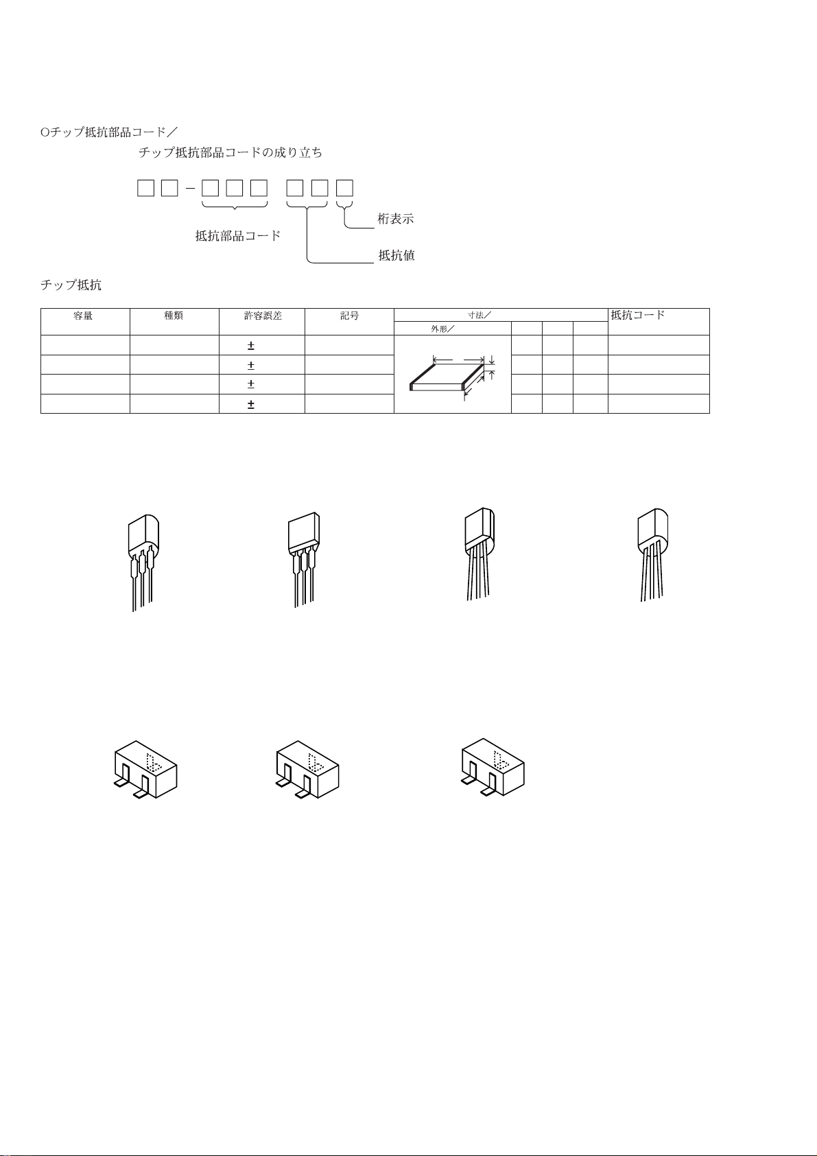
CHIP RESISTOR PART CODE
Chip Resistor Part Coding
88
A
Resistor Code
Chip resistor
Wattage Type Tolerance
1/16W 1005 5% CJ
1/16W
1/10W
1/8W
1608
2125
3216
5%
5%
5%
TRANSISTOR ILLUSTRATION
E C B
E C B
Symbol
CJ
CJ
CJ
Figure
Value of resistor
Form
L
Dimensions (mm)
t
W
E C B
0.55
Resistor Code
108
118
128
E C B
LW t
1.0 0.5 0.35 104
1.6 0.8 0.45
2 1.25 0.45
3.2
1.6
: A
: A
CSC4115BC
CSD655E
KTC3198GR
D
G
S
2SK2158
2SJ461-T1
2SC4115SRS
S
D
G
2SK360E
2SA1318T
B
2SC2714O
2SC3052F
CSD1306E
KRA102S
2SA1979O/Y
C
E
KRA107S
KRC102S-RTK
KRC107S
– 8 –
Page 9
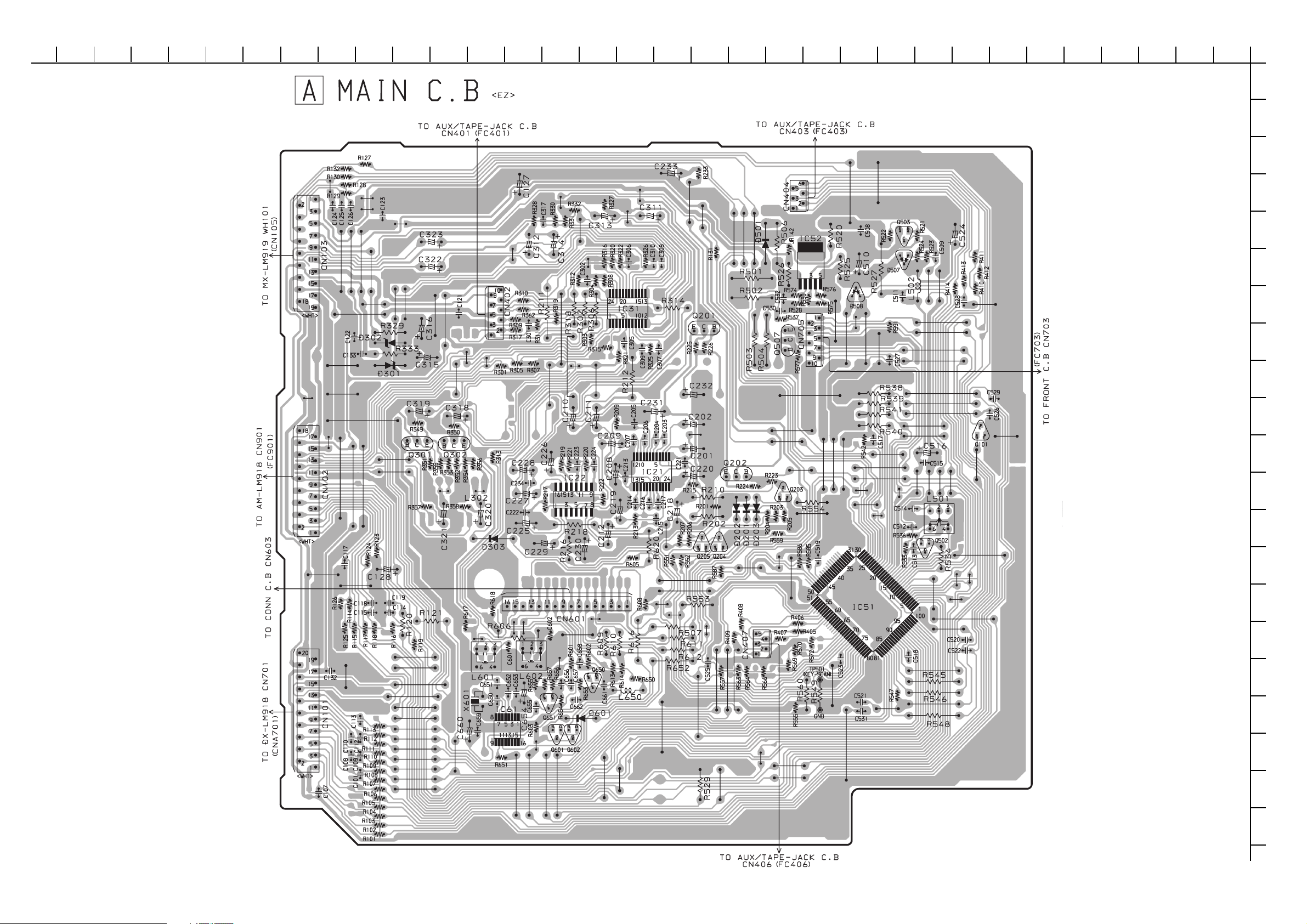
WIRING – 1 (MAIN) <EZ>
32 31 30 29 28 27 26 25 24 23 22 21 20 19 18 17 16 15 14 13 12 11 10 9 8 7 6 5 4 3 2 1
A
B
C
D
E
F
G
H
I
J
K
L
M
N
O
P
Q
– 9 –
R
S
T
U
Page 10
WIRING – 2 (MAIN) <K>
32 31 30 29 28 27 26 25 24 23 22 21 20 19 18 17 16 15 14 13 12 11 10 9 8 7 6 5 4 3 2 1
A
B
C
D
E
F
G
H
I
J
K
L
M
N
O
P
Q
– 10 –
R
S
T
U
Page 11
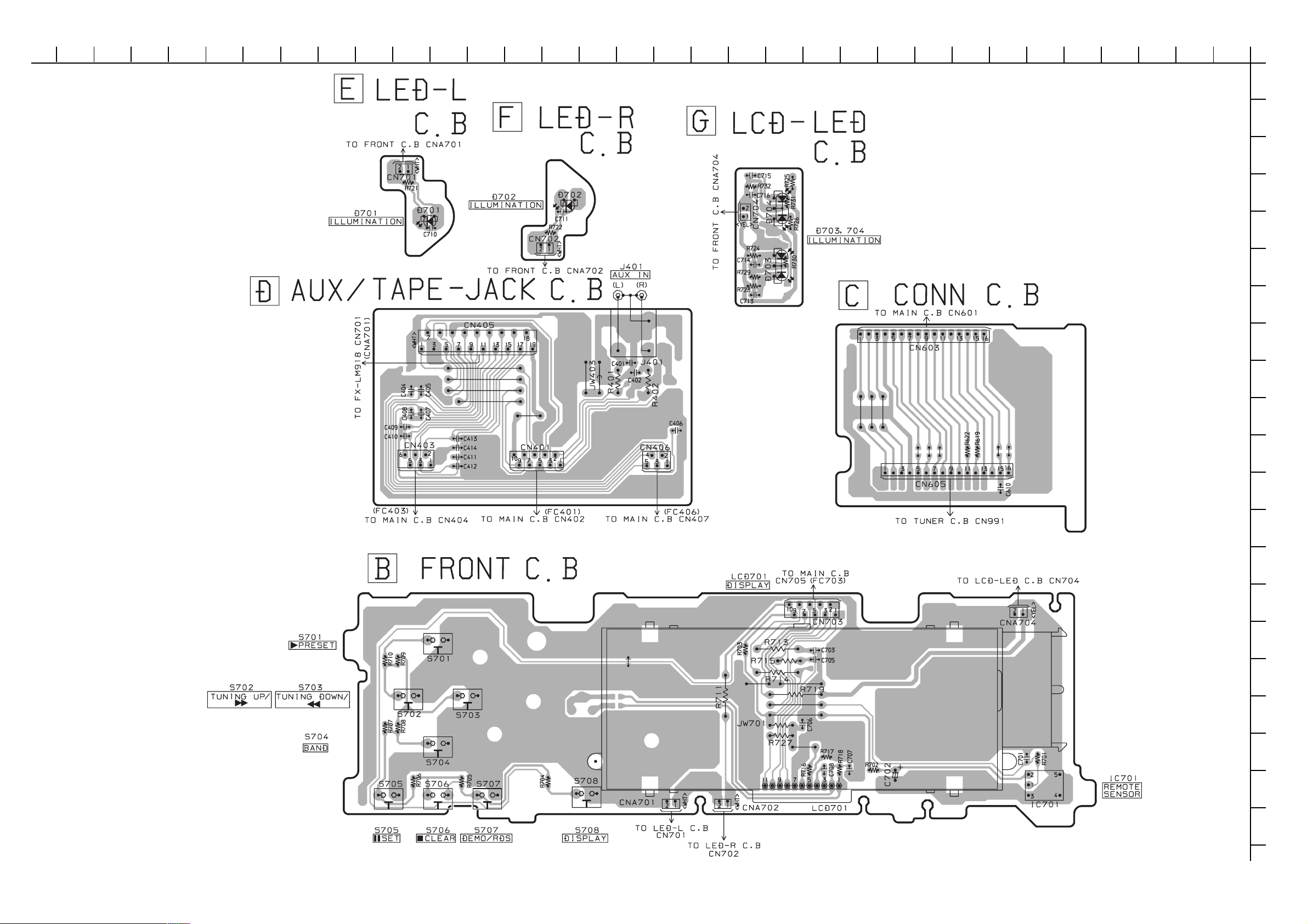
WIRING 3 (FRONT / CONN / AUX / TAPE JACK / LED L / LED R / LCD LED) <EZ>
32 31 30 29 28 27 26 25 24 23 22 21 20 19 18 17 16 15 14 13 12 11 10 9 8 7 6 5 4 3 2 1
A
B
C
D
E
F
G
H
I
J
K
L
M
N
O
P
Q
11
R
S
T
U
Page 12
WIRING 4 (FRONT / CONN / AUX / TAPE JACK / LED L / LED R / LCD LED) <K>
32 31 30 29 28 27 26 25 24 23 22 21 20 19 18 17 16 15 14 13 12 11 10 9 8 7 6 5 4 3 2 1
A
B
C
D
E
F
G
H
I
J
K
L
M
N
O
P
Q
12
R
S
T
U
Page 13
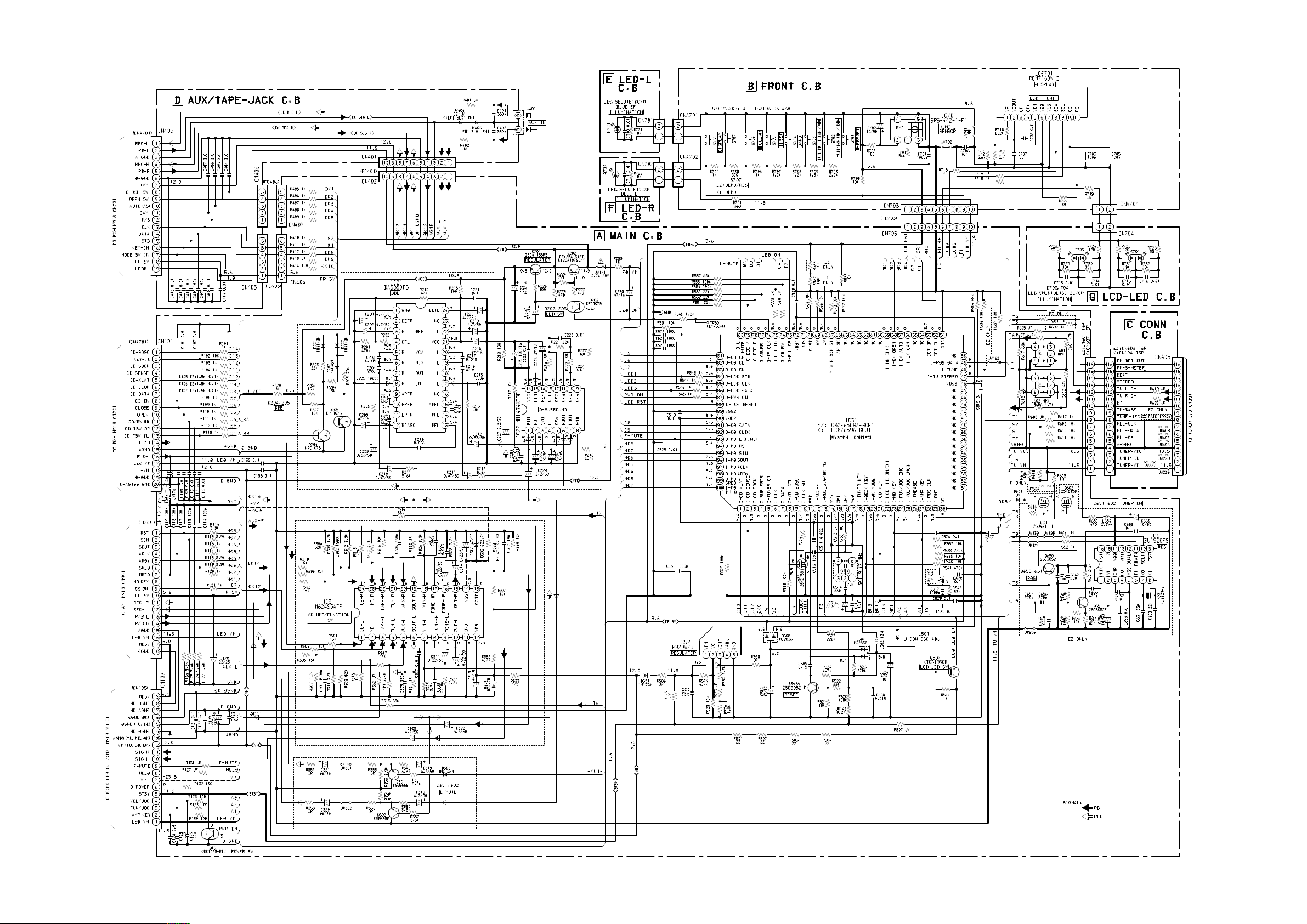
SCHEMATIC DIAGRAM – 1 (MAIN / FRONT / CONN / AUX / TAPE – JACK / LED – L / LED – R / LCD – LED)
– 13 –
Page 14
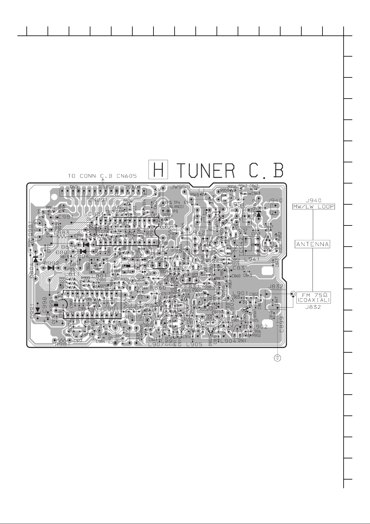
WIRING 5 (TUNER)
151413121110987654321
A
B
C
D
E
F
G
H
I
J
K
L
M
N
O
P
Q
14
R
S
T
U
Page 15
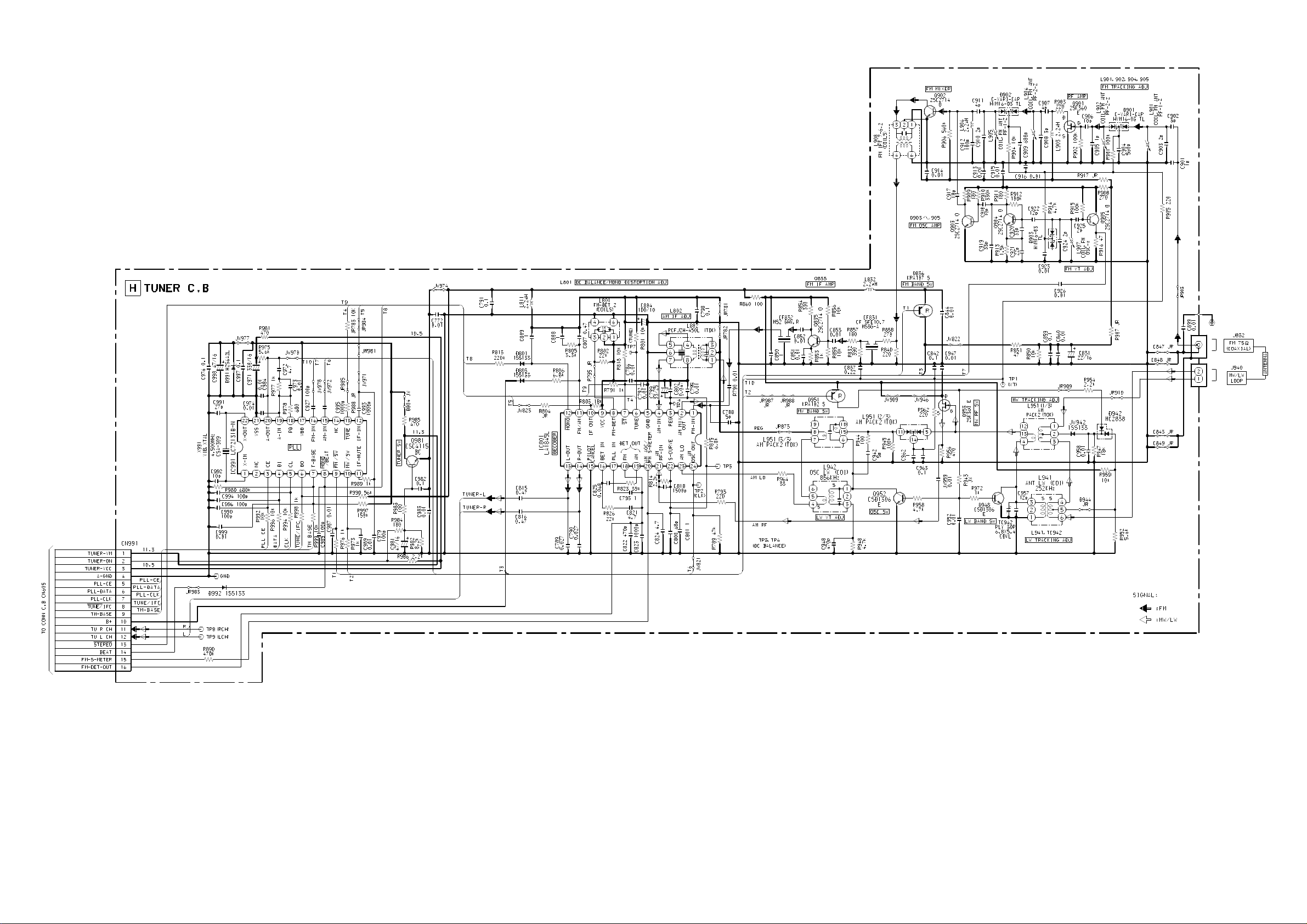
SCHEMATIC DIAGRAM – 2 (TUNER)
– 15 –
Page 16
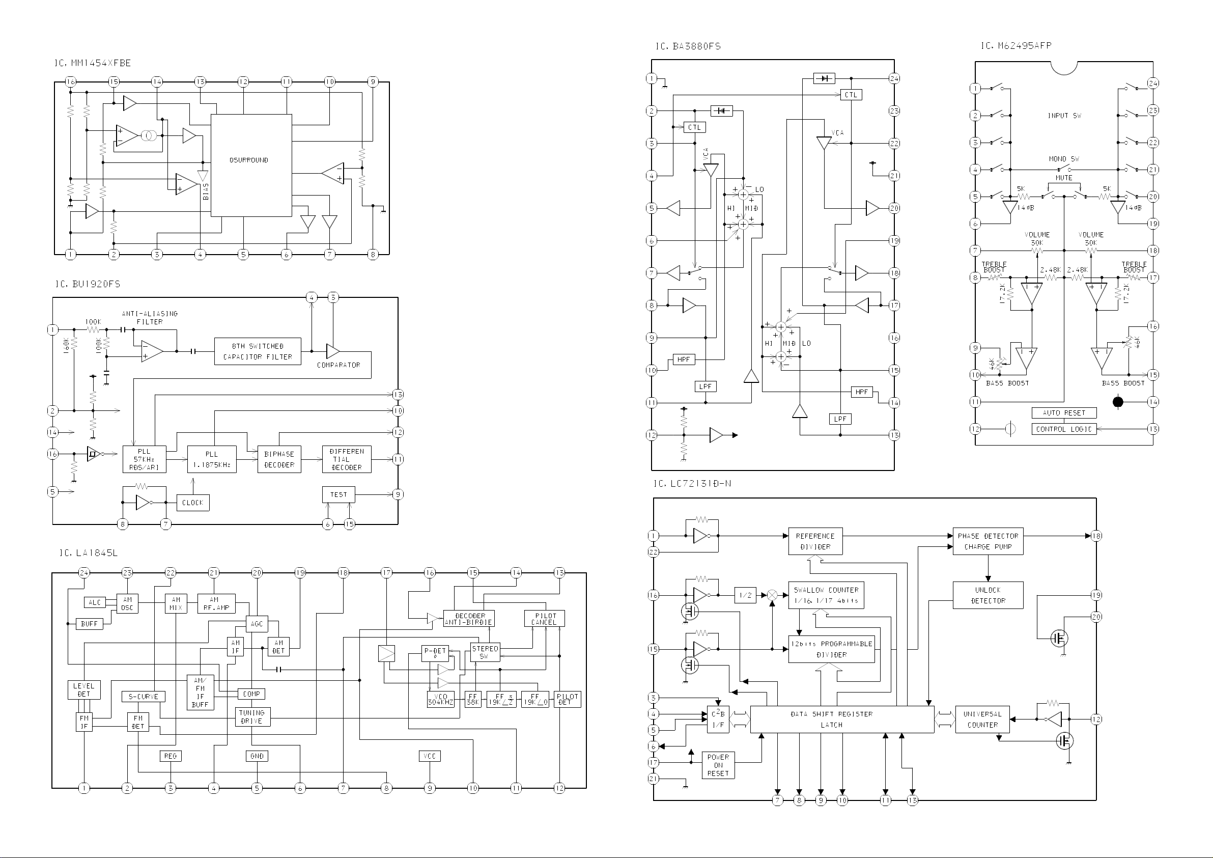
IC BLOCK DIAGRAM
– 16 –
Page 17
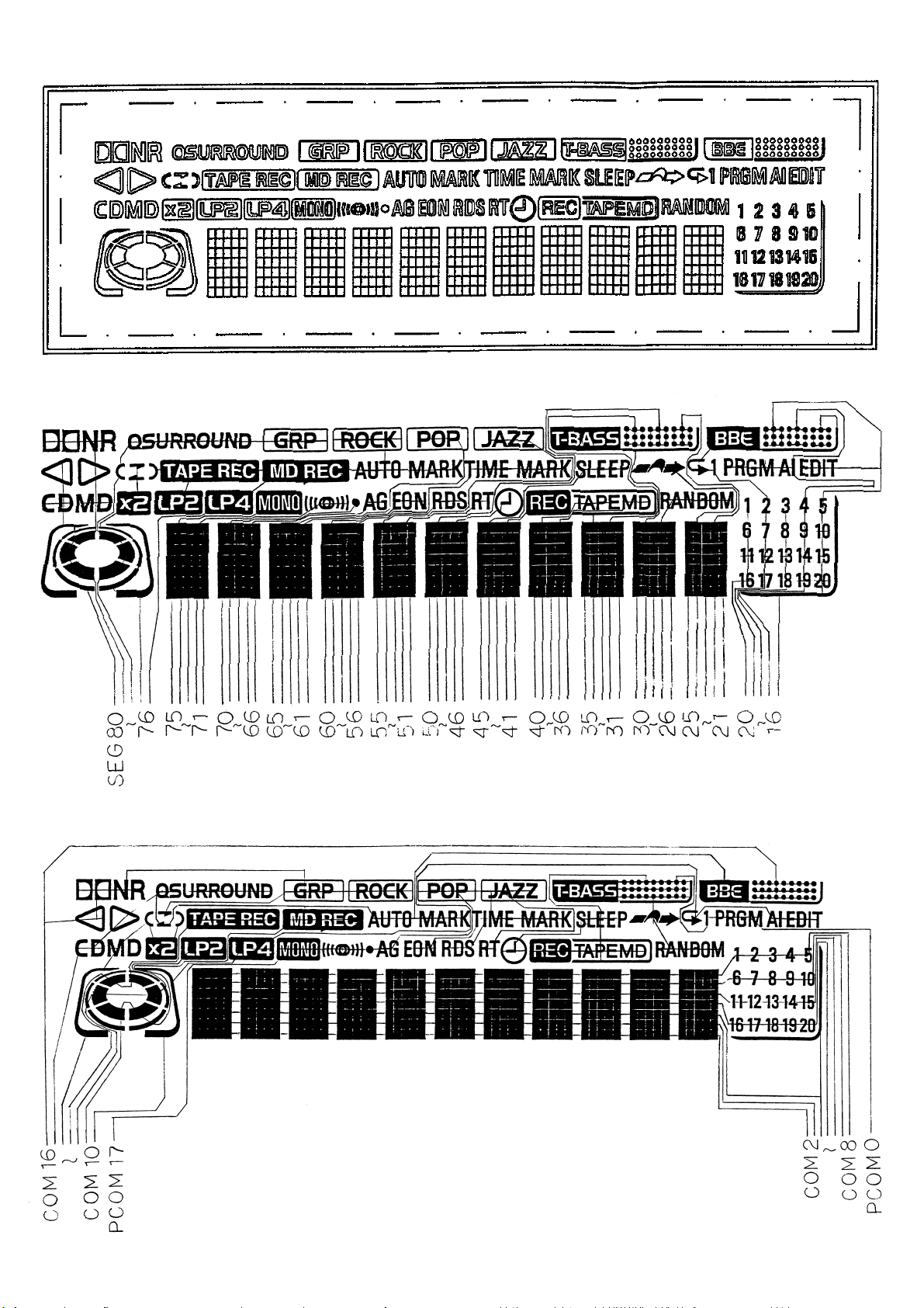
LCD DIAGRAM
Segment side
Common side
17
Page 18

IC DESCRIPTION
EZ : IC, LC87F65C8A-BCF1, K : IC, LC876596-BCJ1
Pin No. Pin Name I/O Description
1 O-CD XLAT O Latch output for CD DSP CXD2589Q 8pin.
2 I-CD SENSE I Sense input for CD DSP CXD2589Q 6pin.
3 O-CD SQCK O SQCK output for CD DSP CXD2589Q 4pin.
4 O-SUB FSTB O Strobe output for deck IC BU2092F 4pin.
5 O-TUNER ON O ON/OFF control for tuner block.
6 O-CLK O Clock output for deck IC BU2092F and tuner PLL IC, LC72131D-N.
7 O-DATA O Data output for deck IC BU2092F and tuner PLL IC, LC72131D-N.
8 O-VOL CTL O VOL/P.EQ IC M62495AFP control.
9 I-CD SQSO I SQSO input for CD DSP CXD2589Q.
10 O-CLK SHIFT O MICON clock shift control.
11 RST I Reset MICON.
12 I-ACOFF I AC OFF detect.
13 I-RDS-SIG/DK MS I RDS signal input (EZ only) / deck MS input.
14 VSS1 – GND.
15 CF1 – Connection of 9.43MHz oscillator.
16 CF2 – Connection of 9.43MHz oscillator.
17 VDD1 – µ-COM 5V.
18 I-TUNER KEY I AD input for tuner key.
19 I-DECK KEY I AD input for deck key.
20 I-DK MODE I AD input for mecha deck position.
21 I-CD KEY I AD input for CD key.
22 O-LCD LED ON/OFF O LCD back light control.
23 I-MD KEY I AD input for MD key.
24 I-FUNC/JOG ENC1 I AD input for FUNC rotary encoder.
25 I-VOL/JOG ENC0 I AD input for VOL rotary encoder.
26 I-TMBASE I Time base clock input.
27 I-AMP KEY I AD input for AMP key.
28 I-RDS CLK I RDS clock input. (EZ only)
29 I-RMT I System remote control signal input.
30 ~ 45 NC – Not connected.
46 VDD3 – µ-COM 5V.
47 I-TU STEREO I Tuner stereo detect input.
48 I-TUNE I Data input for tuner PLL IC, LC72131D-N.
49 I-RDS DATA I RDS data input. (EZ only)
50 NC – Not connected.
51 GND – GND.
52 CDT CL I Input for CD tray close position.
53 CDT OP I Input for CD tray open position.
54, 55 NC – Not connected.
56 I-DK CAM I Input for mecha deck position (CAM).
57 I-DK AUTO I Input for mecha deck condition (AUTO).
58 I-DK OPEN I Input for mecha deck position (OPEN).
– 18 –
Page 19

Pin No. Pin Name I/O Description
59 I-DK CLOSE I Input for mecha deck position (CLOSE).
60 ~ 65 NC – Not connected.
66 AM10K I AM10K option. (Connected to GND through a resistor)
67 FM WIDE&AM ST I FM WIDE & AM ST option. (Connected to GND through a resistor)
68 LW I LW option. (Connected to FR5V through a resistor)
69 SW I SW option. (Connected to GND through a resistor)
70 OIRT I OIRT option. (Connected to GND through a resistor)
71 RDS I
72 VDD4 – µ-COM 5V.
73 O-PLL CE O Chip enable output for tuner PLL IC, LC72131D-N.
74 O-CD RW O CD RW switch control.
75 O-LED ON O Light LED control.
76 O-TP CLK O MICON clock test point. (Connected to GND through a resistor)
77 O-QSURR O Q-SURROUND IC ON/OFF control.
78 O-BBE B O BBE IC control output B.
79 O-BBE A O BBE IC control output A.
RDS option. (K : Connected to GND through a resistor)
(EZ : Connected to FR5V through a resistor)
80 O-L MUTE O Line out mute control.
81 O-CD OP O Output for CD tray open control.
82 O-CD CL O Output for CD tray close control.
83 O-CD ON O Output for CD block ON/OFF control.
84 O-LCD STB O Strobe output for LCD driver.
85 O-LCD CLK O Clock for LCD driver control.
86 O-LCD DATA O Data for LCD driver control.
87 O-PWR ON O Set power ON/OFF output.
88 O-LCD RESET O Reset for LCD driver control.
89 VSS2 – GND.
90 VDD2 – µ-COM 5V.
91 O-CD DATA O Data for CD DSP CXD2589Q 7pin.
92 O-CD CLOK O Clock for CD SP CXD2589Q 9pin.
93 O-MUTE (FUNC) O Output of main mute.
94 O-MD RST O Reset control for MD unit.
95 O-MD SIN O Serial data output for MD unit.
96 I-MD SOUT I Serial data input for MD unit.
97 I-MD ACLK I Clock input for MD unit.
98 O-MD ARDY O Serial data standby for MD unit.
99 O-MD SREQ O Serial data request for MD unit.
100 I-MD MREQ I Serial data request from MD unit.
– 19 –
Page 20

ADJUSTMENT
< TUNER SECTION >
1. Clock Frequency Check
Settings : • Test point : TP2 (CLK)
Method : Set to MW 1602kHz and check that the test point is
2052kHz ± 45Hz.
2. MW VT Check
Settings : • Test point : TP1 (VT)
Method : Set to MW 1602kHz and check that the test point is
less than 8.0V. Then set to MW 531kHz and check
that the test point is more than 0.6V.
3. MW Tracking Adjustment
Settings : • Test point : TP8 (Rch), TP9 (Lch)
• Adjustment location : L951 (1/3)
Method : Set to MW 999kHz and adjust L951 (1/3) so that the
test point becomes maximum.
4. LW VT Adjustment
Settings : • Test point : TP1 (VT)
• Adjustment location : L942
Method : Set to LW 144kHz and adjust L942 so that the test
point becomes 1.3V ± 0.05V.
Then set to LW 290kHz and check that the test point
is less than 8.0V.
5. LW Tracking Adjustment
Settings : • Test point : TP8 (Rch), TP9 (Lch)
• Adjustment location :
L941 ........................... 144kHz
TC942......................... 290kHz
Method : Set up TC942 to center before adjustment. The level at
144kHz is adjusted to MAX by L941. Then the level
at 290kHz is adjusted to MAX by TC942.
8. FM Tracking Adjustment
Settings : • Test point : TP8 (Rch), TP9 (Lch)
• Adjustment location :L901, L902, L904, L905
Method : Set to FM 108.0MHz and adjust L901, L902, L904,
L905 so that the test point becomes maximum with
minimum distorion. Then set to FM 98.0MHz and
check that the test point is less than 13dBµV.
9. DC Balance / Mono Distortion Adjustment
Settings : • Test point : TP3, TP4 (DC balance)
TP8 (Rch), TP9 (Lch)
(Mono Distortion)
• Adjustment location :L801
• Input level : 60dBµV
Method : Set to FM 98.0MHz and adjust L801 so that the
voltage between TP3 and TP4 becomes 0V ± 500mV.
Next, check that the distortion is less than 1.2%.
< MAIN SECTION >
10. µ-CON OSC Adjustment
Settings : • Test point : TP501 (KEY-SCAN) and (GND)
• Adjustment location : L501
Method : Insert AC plug while pressing POWER key and
BAND function key. Then adjust L501 so that the
frequency at the test point becomes 97.256 ± 0.097Hz.
6. AM IF Adjustment
Settings : • Test point : TP8 (Rch), TP9 (Lch)
• Adjustment location :
L802 ........................... 450kHz
7. FM VT Adjustment
Settings : • Test point : TP1 (VT)
• Adjustment location : L907
Method : Set to FM 108.0MHz and adjust L907 so that the test
point becomes 7.0V ± 0.05V. Then set to
FM 87.5MHz and check that the test point is more
than 0.5V.
– 20 –
Page 21

MECHANICAL EXPLODED VIEW 1 / 1 <EZ>
PWB
12
PWB
13
14
C
15
C
24
PWB
PWB
23
D
C
B
16
17
D
10
11
SH,LCD
LCD
SH,REFRECTOR
8
PWB
5
3
A
2
4
7
PWB
6
PWB
C
9
21
C
18
PWB
CHAS,MAIN
C
C
C
19
C
21
C
1
E
A
A
22
20
– 21 –
Page 22

MECHANICAL PARTS LIST 1 / 1 <EZ>
PART NO.
NO.
1 8B-CF1-004-010 WINDOW,DISPLAY
2 8Z-CC3-007-010 BADGE,AIWA 27.5 ABS SIL
3 8B-CF1-012-010 CABI,FR TU EZ
4 8B-CF1-003-010 WINDOW,SENSOR
5 8B-CE1-018-010 REFLECTOR,FR
6 8Z-CE3-204-010 GUIDE,LED R
7 8B-CE1-208-010 GUIDE,LED CNT
8 8Z-CE3-203-010 GUIDE,LED L
9 8B-CF1-005-010 PANEL,SIDE L
10 8B-CF1-204-010 HLDR,LCD
11 8B-CF1-007-010 REFLECTOR,LCD
12 8B-CF1-203-010 GUIDE,LCD
13 88-910-151-110 FF-CABLE, 10P 1.25 150MM
14 8B-CF1-011-010 PANEL,TOP
15 8B-CF1-205-010 PLATE,TOP
16 88-906-151-110 FF-CABLE,6P 1.25
17 88-910-101-110 FF-CABLE, 10P 1.25 100MM
18 88-905-151-110 FF-CABLE, 5P 1.25 150MM
19 8B-CF1-009-010 PANEL,REAR TU EZ
20 8B-CF1-006-010 PANEL,SIDE R
21 8B-CE1-016-010 FOOT,DIA40 H4
22 8B-CF1-002-010 KEY,TUNER
23 8B-CE1-212-010 PLATE, TOP A
24 8B-CE1-213-010 PLATE, TOP B
A 87-721-096-410 QT2+3-10 GLD
B 87-B10-294-010 BVT2+2.6-8
C 87-067-703-010 TAPPING SCREW, BVT2+3-10
D 87-067-684-010 BVT2+2.6- W/O SLOT
E 8Z-CL1-034-010 S-SCREW,ZCL1
DESCRIPTIONREF. NO. KANRI
COLOR NAME TABLE
Basic color symbol Color Basic color symbol Color Basic color symbol Color
B Black C Cream D Orange
G Green H Gray L Blue
LT Transparent Blue N Gold P Pink
R Red S Silver ST Titan Silver
T Brown V Violet W White
WT Transparent White Y Yellow YT Transparent Yellow
LM Metallic Blue LL Light Blue GT Transparent Green
LD Dark Blue DT Transparent Orange GM Metallic Green
YM Metallic Yellow DM Metallic Orange PT Transparent Pink
LA Aqua Blue GL Light Green HT Transparent Gray
– 22 –
Page 23

MECHANICAL EXPLODED VIEW 1 / 1 <K>
PWB
12
PWB
13
14
24
23
D
B
16
C
PWB
PWB
17
D
C
10
11
SH,LCD
LCD
SH,REFRECTOR
8
PWB
5
3
A
2
4
7
6
PWB
15
PWB
C
9
C
18
PWB
CHAS,MAIN
C
C
C
19
C
21
1
E
A
A
22
C
20
– 23 –
Page 24

MECHANICAL PARTS LIST 1 / 1 <K>
PART NO.
NO.
1 8B-CF1-004-010 WINDOW,DISPLAY
2 8Z-CC3-007-010 BADGE,AIWA 27.5 ABS SIL
3 8B-CF1-001-010 CABI,FR TU
4 8B-CF1-003-010 WINDOW,SENSOR
5 8B-CE1-018-010 REFLECTOR,FR
6 8Z-CE3-204-010 GUIDE,LED R
7 8B-CE1-208-010 GUIDE,LED CNT
8 8Z-CE3-203-010 GUIDE,LED L
9 8B-CF1-005-010 PANEL,SIDE L
10 8B-CF1-204-010 HLDR,LCD
11 8B-CF1-007-010 REFLECTOR,LCD
12 8B-CF1-203-010 GUIDE,LCD
13 88-910-151-110 FF-CABLE, 10P 1.25 150MM
14 8B-CF1-011-010 PANEL,TOP
15 8B-CF1-205-010 PLATE,TOP
16 88-906-151-110 FF-CABLE,6P 1.25
17 88-910-101-110 FF-CABLE, 10P 1.25 100MM
18 88-905-151-110 FF-CABLE, 5P 1.25 150MM
19 8B-CF1-013-010 PANEL,REAR TU K
20 8B-CF1-006-010 PANEL,SIDE R
21 8B-CE1-016-010 FOOT,DIA40 H4
22 8B-CF1-002-010 KEY,TUNER
23 8B-CE1-212-010 PLATE,TOP A
24 8B-CE1-213-010 PLATE,TOP B
A 87-721-096-410 QT2+3-10 GLD
B 87-B10-294-010 BVT2+2.6-8
C 87-067-703-010 TAPPING SCREW, BVT2+3-10
D 87-067-684-010 BVT2+2.6- W/O SLOT
E 8Z-CL1-034-010 S-SCREW,ZCL1
DESCRIPTIONREF. NO. KANRI
COLOR NAME TABLE
Basic color symbol Color Basic color symbol Color Basic color symbol Color
B Black C Cream D Orange
G Green H Gray L Blue
LT Transparent Blue N Gold P Pink
R Red S Silver ST Titan Silver
T Brown V Violet W White
WT Transparent White Y Yellow YT Transparent Yellow
LM Metallic Blue LL Light Blue GT Transparent Green
LD Dark Blue DT Transparent Orange GM Metallic Green
YM Metallic Yellow DM Metallic Orange PT Transparent Pink
LA Aqua Blue GL Light Green HT Transparent Gray
– 24 –
Page 25

MODEL NO.
MX-LM918 / LM919
ELECTRICAL MAIN PARTS LIST
PART NO.
NO.
IC
87-001-536-010 IC,NJM78M05FA
87-A22-097-010 IC,KIA7812AP
TRANSISTOR
87-026-609-080 TR,KTA1266GR
87-A30-076-080 C-TR,2SC3052F
87-A30-075-080 C-TR,2SA1235F
87-A30-268-040 C-TR,2SA1514K(S)
87-A30-074-080 C-TR,RT1P 141C
87-A30-196-080 TR,2SC4115SRS
89-406-555-080 TR,2SD655E
87-A30-105-080 C-TR,RT1P 441C
87-A30-190-080 TR,CC5551
87-A30-214-010 TR,2SB1344
87-A30-215-010 TR,2SD2025
87-A30-106-070 C-TR,CMBT5551
87-A30-087-080 C-FET,2SK2158
DIODE
87-A40-004-080 ZENER,MTZJ16A
87-A40-291-080 DIODE,1N4148M (CPT)
87-A40-269-080 C-DIODE,MC2836
87-A40-270-080 C-DIODE,MC2838
87-070-178-090 DIODE,1N5402-BD54
87-A40-488-080 DIODE,1SS244
87-A40-299-080 ZENER,DZ5.1M
87-070-274-080 DIODE,1N4003 SEM
PWB-AMP C.B
C101 87-A12-066-080 CAP,E 47-16 SMG
C103 87-A12-091-080 CAP,E 10-50 SMG
C105 87-010-496-080 CAP,E 3.3-50 M 5L SRE
C106 87-010-555-080 CAP,E 100-10 GAS
C107 87-012-286-080 CAP,U 0.01-25 K B
C108 87-010-494-080 CAP,E 1-50 M 5L SRE
C110 87-A12-071-080 CAP,E 47-25 SMG
C111 87-A10-918-080 CAP,E 100-16 SMG
C112 87-A10-918-080 CAP,E 100-16 SMG
C113 87-012-286-080 CAP,U 0.01-25 K B<EZ>
C114 87-012-284-080 CAP,U 6800P-50 K B
C115 87-A12-066-080 CAP,E 47-16 SMG
C116 87-012-284-080 CAP, U 6800P-50
C117 87-012-278-080 C-CAP,U 2200P-50 B
C118 87-012-278-080 C-CAP,U 2200P-50 B
C119 87-A12-085-080 CAP,E 0.33-50 SMG
C120 87-A12-085-080 CAP,E 0.33-50 SMG
C121 87-012-272-080 C-CAP,U 680P-50 K B
C122 87-012-272-080 C-CAP,U 680P-50 K B
C123 87-A12-440-000 CAP,E 3300-35 M 85 IV LELON
C124 87-A12-440-000 CAP,E 3300-35 M 85 IV LELON
C125 87-012-273-080 C-CAP,U 820P-50 B
C126 87-012-273-080 C-CAP,U 820P-50 B
C127 87-012-282-080 CAP, U 4700P-50
C128 87-012-282-080 CAP, U 4700P-50
C129 87-012-167-080 C-CAP,U 5P-50 CH
C130 87-012-167-080 C-CAP,U 5P-50 CH
C131 87-A12-091-080 CAP,E 10-50 SMG
C132 87-A12-071-080 CAP,E 47-25 SMG
C135 87-A12-091-080 CAP,E 10-50 SMG
C136 87-A12-071-080 CAP,E 47-25 SMG
DESCRIPTIONREF. NO. KANRI
PART NO.
C137 87-012-199-080 C-CAP,U 220P-50 J CH
C138 87-012-199-080 C-CAP,U 220P-50 J CH
C139 87-012-199-080 C-CAP,U 220P-50 J CH
C140 87-012-199-080 C-CAP,U 220P-50 J CH
C142 87-A12-317-080 C-CAP,U 0.1-50 Z F
C143 87-A12-317-080 C-CAP,U 0.1-50 Z F
C146 87-A12-317-080 C-CAP,U 0.1-50 Z F
C147 87-A12-317-080 C-CAP,U 0.1-50 Z F
C148 87-012-282-080 C-CAP,U 4700P-50 K B
C149 87-012-282-080 C-CAP,U 4700P-50 K B
C150 87-010-831-080 C-CAP,U 0.1-16 Z F<EZ>
C401 87-A10-831-080 CAP,E 1000-25 M SMG
CN101 87-099-545-010 CONN,14P V BLK TKC-M
CN102 87-A60-624-010 CONN,7P V 2MM JMT
CN103 87-A60-539-010 CONN,5P V TUC-P05P-B1
CN104 87-049-469-010 CONN,4P V WHT EH
J101 87-099-801-010 JACK,PIN 1P BLK W/O SW
L100 87-003-143-080 COIL,4.7UH K LAL02
L101 87-003-098-080 COIL,2.2UH K LAL02
R188 87-A00-258-080 RES,M/F 0.22-1W J
R189 87-A00-258-080 RES,M/F 0.22-1W J
R190 87-A00-258-080 RES,M/F 0.22-1W J
R191 87-A00-258-080 RES,M/F 0.22-1W J
R192 87-A00-258-080 RES,M/F 0.22-1W J
R193 87-A00-258-080 RES,M/F 0.22-1W J
TH51 87-A91-042-080 C-THMS,100K 55001
TH52 87-A91-042-080 C-THMS,100K 55001
WH101 87-A61-039-010 CONN,19P V WHT 52328
SPK C.B
C600 87-010-384-040 CAP,E 100-25 M 11L SME
C601 87-010-384-040 CAP,E 100-25 M 11L SME
C602 87-010-384-040 CAP,E 100-25 M 11L SME
C603 87-012-278-080 C-CAP,U 2200P-50 B
C604 87-012-278-080 C-CAP,U 2200P-50 B
C605 87-A11-174-090 CAP,E 4700-16 M SMG
C606 87-A12-755-000 CAP,E 4700-25 M 85 IV LELON<EZ>
C606 87-A12-829-000 CAP,E 4700-25 M 85 GS<K>
C607 87-A12-317-080 C-CAP,U 0.1-50 Z F
C608 87-A12-317-080 C-CAP,U 0.1-50 Z F
C609 87-010-758-080 C-CAP,U 0.068-25 Z F CM/CB
C610 87-010-758-080 C-CAP,U 0.068-25 Z F CM/CB
C611 87-010-759-080 C-CAP,U 0.1-25F
C612 87-010-759-080 C-CAP,U 0.1-25F
C613 87-010-759-080 C-CAP,U 0.1-25F
C614 87-010-759-080 C-CAP,U 0.1-25F
C615 87-010-759-080 C-CAP,U 0.1-25F
C616 87-010-759-080 C-CAP,U 0.1-25F
CN600 87-009-799-010 CONN,14P H BLK TKC-M
CN601 87-049-469-010 CONN,4P V WHT EH
CN602 87-099-407-010 CONN,7P V WHT EH
J600 87-A60-659-010 TERMINAL,SPKR 4P HSP-134V-05Z
L600 87-003-383-010 COIL,1UH K
L601 87-003-383-010 COIL,1UH K
L602 87-003-098-080 COIL,2.2UH K LAL02
L603 87-003-098-080 COIL,2.2UH K LAL02
L604 87-003-098-080 COIL,2.2UH K LAL02
!
PR600 87-026-681-080 PROTECTOR,5A 491SERIES 60V
!
PR601 87-026-681-080 PROTECTOR,5A 491SERIES 60V
!
PR602 87-026-681-080 PROTECTOR,5A 491SERIES 60V
FRONT C.B
C300 87-A12-071-080 CAP,E 47-25 SMG
NO.
DESCRIPTIONREF. NO. KANRI
– 25 –
Page 26

PART NO.
NO.
C301 87-012-286-080 C-CAP,U 0.01-25 K B
C302 87-012-286-080 C-CAP,U 0.01-25 K B
C303 87-012-286-080 C-CAP,U 0.01-25 K B
C304 87-012-286-080 C-CAP,U 0.01-25 K B
C305 87-012-286-080 C-CAP,U 0.01-25 K B
C306 87-012-286-080 C-CAP,U 0.01-25 K B
CNA301 88-805-072-090 CONN ASSY,7P 2.0 200MM
CNA302 88-805-020-790 CONN ASSY,2P 70MM
CNA303 88-805-020-790 CONN ASSY,2P 70MM
D302 87-A40-317-080 LED,SLR-342VCT31 RED
D303 87-A40-640-010 LED,SELU1E10CXM BLUE-EF
D304 87-A40-640-010 LED,SELU1E10CXM BLUE-EF
S301 87-A90-696-080 SW,TACT TS2103-03-430
S302 87-A90-696-080 SW,TACT TS2103-03-430
S303 87-A90-696-080 SW,TACT TS2103-03-430
S304 87-A90-696-080 SW,TACT TS2103-03-430
S305 87-A90-696-080 SW,TACT TS2103-03-430
SW300 87-A92-202-010 SW,RTRY RE012302PVB25 FUNC
SW301 87-A92-203-010 SW,RTRY RE012305PVB25 JOG
HP C.B
C617 87-012-280-080 C-CAP,U 3300P-50 K B
C618 87-012-280-080 C-CAP,U 3300P-50 K B
CNA501 8B-CE1-622-010 CONN ASSY,7P 240MM
J501 87-A60-420-010 JACK,3.5 ST (MSC)
DESCRIPTIONREF. NO. KANRI
PART NO.
LED-L C.B
C701 87-012-286-080 C-CAP,U 0.01-25 K B
CN702 87-A60-619-010 CONN,2P V 2MM JMT
D700 87-A40-640-010 LED,SELU1E10CXM BLUE-EF
LED-R C.B
C702 87-012-286-080 C-CAP,U 0.01-25 K B
CN703 87-A60-619-010 CONN,2P V 2MM JMT
D701 87-A40-640-010 LED,SELU1E10CXM BLUE-EF
AC C.B
!
C404 87-A10-479-080 CAP,CER 2200P-250 M E KH
CN401 87-A60-538-010 CONN,5P H TUC-P05X-B1
CN402 87-A60-619-010 CONN,2P V 2MM JMT
!
PT401 8B-NF9-665-010 PT,SUB BNF E (TAM)
!
PT403 8B-CE1-613-010 PT,EZ
!
RY401 87-A90-976-010 RELAY,AC12V SDT-S-112LMR
!
TM401 87-A60-317-010 TERMINAL, 1P MSC
!
TM402 87-A60-317-010 TERMINAL, 1P MSC
NO.
DESCRIPTIONREF. NO. KANRI
CHIP RESISTOR PART CODE
Chip Resistor Part Coding
88
A
Resistor Code
Chip resistor
Wattage Type Tolerance
1/16W 1005 5% CJ
1/16W
1/10W
1/8W
1608
2125
3216
5%
5%
5%
Symbol
CJ
CJ
CJ
Figure
Value of resistor
Form
L
Dimensions (mm)
t
W
0.55
Resistor Code
108
118
128
LW t
1.0 0.5 0.35 104
1.6 0.8 0.45
2 1.25 0.45
3.2
1.6
: A
: A
– 26 –
Page 27

TRANSISTOR ILLUSTRATION
E C B
CC5551
KTA1266GR
E C B
2SC4115SRS
E C B
2SD655E
G
S
2SK2158
B C E
2SD2025
D
B
C
E
B C E
2SB1344
2SA1235F
2SA1514K(S)
2SC3052F
CMBT5551
R T1P141C
R T1P441C
– 27 –
Page 28

WIRING – 1 (PWB – AMP / HP)
32 31 30 29 28 27 26 25 24 23 22 21 20 19 18 17 16 15 14 13 12 11 10 9 8 7 6 5 4 3 2 1
A
B
C
D
E
F
G
H
I
J
K
L
M
N
O
P
Q
– 28 –
R
S
T
U
Page 29

WIRING 2 (SPK / FRONT / LED L / LED R / AC)
32 31 30 29 28 27 26 25 24 23 22 21 20 19 18 17 16 15 14 13 12 11 10 9 8 7 6 5 4 3 2 1
A
B
C
D
E
F
G
H
I
J
K
L
M
N
O
P
Q
29
R
S
T
U
Page 30

SCHEMATIC DIAGRAM (PWB – AMP / SPK / FRONT / HP / LED – L / LED – R / AC)
– 30 –
Page 31

MECHANICAL EXPLODED VIEW 1 / 1 <EZ>
C
C
18
17
E
C
30
D
16
PWB
HT-SINK MAIN
SUB ASSY
C
28
C
HT-SINK REG SA
C
HT-SINK ASSY MAIN
C
C
C
PWB
HLDR,
PWB ECO
25
PWB
C
PLA TE,SHLD AMP
19
20
WIRE ASSY
29
E
E
PWB
PWB
PWB, HLDR
B
12
A
7
3
2
1
5
4
11
6
15
14
10
A
8
A
PWB
CHAS,MAIN
13
PWB
9
26
B
C
26
C
A
C
23
C
27
22
C
C
C
21
C
24
– 31 –
Page 32

MECHANICAL PARTS LIST 1 / 1 <EZ>
PART NO.
1 8B-CE1-011-010 KNOB,RTRY FUN
2 8B-CE1-015-010 LENS,FUN
3 8B-CE1-006-010 RING,FUN
4 8B-CE1-012-010 KNOB,RTRY VOL
5 8B-CE1-008-010 REFLECTOR,VOL
6 8B-CE1-007-010 RING,VOL
7 8Z-CC3-007-010 BADGE,AIWA 27.5 ABS SIL
8 8B-CE1-023-010 CABI,FR AMP EZ
9 8B-CE1-014-010 KEY,JOG MODE
10 8B-CE1-013-010 KEY,ENTER
11 8B-CE1-018-010 REFLECTOR,FR
12 8B-CE1-025-010 KEY ASSY,POWER
13 8Z-CE3-204-010 GUIDE,LED R
14 8B-CE1-208-010 GUIDE,LED CNT
15 8Z-CE3-203-010 GUIDE,LED L
16 8B-CE1-002-010 PANEL,SIDE L AMP
17 8Z-CE3-208-010 PLATE,TOP AMP
18 8B-CE1-005-010 PANEL,TOP AMP
19 87-A80-157-010 AC CORD ASSY,E BLK CC
!
20 87-085-185-010 BUSHING, AC CORD (E)
21 8B-CE1-019-010 PANEL,REAR AMP
22 8B-CE1-017-010 COVER, FAN
23 8B-CL5-616-010 FAN,F410T-12LC-200MM
24 8B-CF1-006-010 PANEL,SIDE R
25 87-003-317-010 F-BEAD,F0H2515-LG7
26 8B-CE1-016-010 FOOT,DIA40 H4
27 8B-CE1-004-010 COVER, CHAS MAIN
!
28 8B-CE1-613-010 PT,EZ
29 8B-CE1-212-010 PLATE, TOP A
30 8B-CE1-213-010 PLATE, TOP B
A 87-591-095-410 TAPPING SCREW, QIT+3-8 (GLD)
B 87-B10-294-010 BVT2+2.6-8
C 87-067-703-010 TAPPING SCREW, BVT2+3-10
D 87-067-586-010 TAPPING SCREW, BVT2+4-8
E 87-067-684-010 BVT2+2.6-6 W/O SLOT
NO.
DESCRIPTIONREF. NO. KANRI
COLOR NAME TABLE
Basic color symbol Color Basic color symbol Color Basic color symbol Color
B Black C Cream D Orange
G Green H Gray L Blue
LT Transparent Blue N Gold P Pink
R Red S Silver ST Titan Silver
T Brown V Violet W White
WT Transparent White Y Yellow YT Transparent Yellow
LM Metallic Blue LL Light Blue GT Transparent Green
LD Dark Blue DT Transparent Orange GM Metallic Green
YM Metallic Yellow DM Metallic Orange PT Transparent Pink
LA Aqua Blue GL Light Green HT Transparent Gray
– 32 –
Page 33

MECHANICAL EXPLODED VIEW 1 / 1 <K>
C
C
18
17
C
F
D
30
16
PWB
HT-SINK MAIN
SUB ASSY
C
28
F
HT-SINK REG SA
C
HT-SINK ASSY MAIN
C
C
C
PWB
HLDR,
PWB ECO
25
PWB
C
PLATE,SHLD AMP
19
20
WIRE ASSY
29
E
E
PWB
PWB
PWB, HLDR
B
12
A
7
3
2
1
5
4
11
6
15
14
10
A
8
A
PWB
CHAS,MAIN
13
PWB
9
26
B
C
26
C
A
C
23
G
27
22
F
F
F
21
F
24
– 33 –
Page 34

MECHANICAL PARTS LIST 1 / 1 <K>
PART NO.
1 8B-CE1-011-010 KNOB,RTRY FUN
2 8B-CE1-015-010 LENS,FUN
3 8B-CE1-006-010 RING,FUN
4 8B-CE1-012-010 KNOB,RTRY VOL
5 8B-CE1-008-010 REFLECTOR,VOL
6 8B-CE1-007-010 RING,VOL
7 8Z-CC3-007-010 BADGE,AIWA 27.5 ABS SIL
8 8B-CE1-001-010 CABI,FR AMP
9 8B-CE1-014-010 KEY,JOG MODE
10 8B-CE1-013-010 KEY,ENTER
11 8B-CE1-018-010 REFLECTOR,FR
12 8B-CE1-025-010 KEY ASSY,POWER
13 8Z-CE3-204-010 GUIDE,LED R
14 8B-CE1-208-010 GUIDE,LED CNT
15 8Z-CE3-203-010 GUIDE,LED L
16 8B-CE1-002-010 PANEL,SIDE L AMP
17 8Z-CE3-208-010 PLATE,TOP AMP
18 8B-CE1-005-010 PANEL,TOP AMP
!
19 87-A80-157-010 AC CORD ASSY,E BLK CC
20 87-085-185-010 BUSHING, AC CORD (E)
21 8B-CE1-019-010 PANEL,REAR AMP
22 8B-CE1-017-010 COVER, FAN
23 8B-CL5-616-010 FAN,F410T-12LC-200MM
24 8B-CF1-006-010 PANEL,SIDE R
25 87-003-317-010 F-BEAD,F0H2515-LG7
26 8B-CE1-016-010 FOOT,DIA40 H4
27 8B-CE1-004-010 COVER, CHAS MAIN
!
28 8B-CE1-613-010 PT,EZ
29 8B-CE1-212-010 PLATE, TOP A
30 8B-CE1-213-010 PLATE, TOP B
A 87-591-095-410 TAPPING SCREW, QIT+3-8 (GLD)
B 87-B10-294-010 BVT2+2.6-8
C 87-067-703-010 TAPPING SCREW, BVT2+3-10
D 87-067-586-010 TAPPING SCREW, BVT2+4-8
E 87-067-684-010 BVT2+2.6-6 W/O SLOT
F 87-067-761-010 BVT2+3-10 BLK
G 87-751-096-410 BVT2+3-10 W/O SLOT
NO.
DESCRIPTIONREF. NO. KANRI
COLOR NAME TABLE
Basic color symbol Color Basic color symbol Color Basic color symbol Color
B Black C Cream D Orange
G Green H Gray L Blue
LT Transparent Blue N Gold P Pink
R Red S Silver ST Titan Silver
T Brown V Violet W White
WT Transparent White Y Yellow YT Transparent Yellow
LM Metallic Blue LL Light Blue GT Transparent Green
LD Dark Blue DT Transparent Orange GM Metallic Green
YM Metallic Yellow DM Metallic Orange PT Transparent Pink
LA Aqua Blue GL Light Green HT Transparent Gray
– 34 –
Page 35

MODEL NO.
DX-LM918
ELECTRICAL MAIN PARTS LIST
PART NO.
NO.
IC
87-A20-547-010 C-IC,CXA1992AR
87-A20-546-010 C-IC,CXD2589Q
87-A20-445-010 IC,BA5936S
87-017-917-080 IC,BU4066BCF
87-001-792-080 IC,NJM2100M
87-017-760-080 IC,M51943BML
87-017-825-010 IC,GP1F32T
TRANSISTOR
87-026-451-080 TR,2SA933SR
89-113-184-080 TR,2SA1318T
87-A30-273-040 C-TR,DTC124EKA
87-A30-047-080 TR,CSD655E
DIODE
87-020-465-080 DIODE,1SS133
87-A40-747-080 ZENER,UZ5.1BSB
MAIN C.B
C701 87-010-497-040 CAP,E 4.7-35 M 5L SRE
C702 87-012-164-080 C-CAP,U 2P-50 C CH
C704 87-A11-070-080 C-CAP,U 0.033-16 K B
C705 87-A11-070-080 C-CAP,U 0.033-16 K B
C706 87-A11-070-080 C-CAP,U 0.033-16 K B
C707 87-A11-070-080 C-CAP,U 0.033-16 K B
C710 87-A11-049-080 C-CAP,U 1-6.3 K B
C711 87-A10-504-080 C-CAP,U 0.047-16 K B
C712 87-A10-504-080 C-CAP,U 0.047-16 K B
C713 87-012-270-080 C-CAP,U 470P-50
C714 87-010-785-080 C-CAP,U0.015-25BK
C715 87-A10-504-080 C-CAP,U 0.047-16 K B
C716 87-A10-504-080 C-CAP,U 0.047-16 K B
C717 87-010-759-080 C-CAP,U, 0.1-25F
C718 87-010-787-080 CAP, U 0.022-25
C719 87-010-555-040 CAP,E 100-10 M 5L SRE
C720 87-010-981-040 CAP,E 22-35 M 5L SRE
C721 87-010-555-040 CAP,E 100-10 M 5L SRE
C722 87-A12-319-080 C-CAP,U 0.1-25 K B
C723 87-A12-319-080 C-CAP,U 0.1-25 K B
C724 87-A12-319-080 C-CAP,U 0.1-25 K B
C725 87-A12-319-080 C-CAP,U 0.1-25 K B
C726 87-012-278-080 C-CAP,U 2200P-50 B
C727 87-010-494-040 CAP,E 1-50 M 5L SRE
C728 87-012-269-080 C-CAP,U 390P-50 B
C729 87-010-555-040 CAP,E 100-10 M 5L SRE
C730 87-012-286-080 CAP, U 0.01-25
C731 87-010-785-080 C-CAP,U0.015-25BK
C732 87-012-276-080 C-CAP,U 1500P-50 K B
C733 87-010-555-040 CAP,E 100-10 M 5L SRE
C734 87-010-555-040 CAP,E 100-10 M 5L SRE
C735 87-010-497-040 CAP,E 4.7-35 M 5L SRE
C736 87-012-286-080 CAP, U 0.01-25
C737 87-A10-189-040 CAP,E 220-10 M 5L
C739 87-012-280-080 CAP, U 3300P-50
C741 87-A12-319-080 C-CAP,U 0.1-25 K B
C743 87-012-286-080 CAP, U 0.01-25
C744 87-A10-730-080 CAP,E 1000-16 SMG
C745 87-A10-504-080 C-CAP,U 0.047-16 K B
C746 87-012-286-080 CAP, U 0.01-25
C747 87-A11-059-080 C-CAP,U 0.47-10 K B
DESCRIPTIONREF. NO. KANRI
PART NO.
NO.
C748 87-012-199-080 C-CAP,U 220P-50 J CH
C749 87-012-284-080 CAP, U 6800P-50
C750 87-010-759-080 C-CAP,U, 0.1-25F
C754 87-012-286-080 CAP, U 0.01-25
C755 87-A12-068-080 CAP,E 470-16 SMG
C756 87-A12-319-080 C-CAP,U 0.1-25 K B
C757 87-A11-049-080 C-CAP,U 1-6.3 K B
C758 87-010-560-040 CAP,E 10-50 M 5L SRE
C759 87-010-759-080 C-CAP,U, 0.1-25F
C760 87-A10-189-040 CAP,E 220-10 M 5L
C761 87-012-180-080 C-CAP,U 22P-50 CH
C762 87-010-553-040 CAP,E 47-16 GAS
C763 87-012-286-080 CAP, U 0.01-25
C764 87-010-759-080 C-CAP,U, 0.1-25F
C765 87-010-981-040 CAP,E 22-35 5L SRE
C766 87-012-286-080 CAP, U 0.01-25
C767 87-012-197-080 C-CAP,U 150P-50 CH
C768 87-012-197-080 C-CAP,U 150P-50 CH
C769 87-A10-759-040 CAP,E 330-6.3 SRM
C770 87-012-286-080 CAP, U 0.01-25
C771 87-012-272-080 C-CAP,U 680P-50 B
C772 87-012-272-080 C-CAP,U 680P-50 B
C773 87-012-172-080 C-CAP,U 10P-50 D CH
C774 87-012-172-080 C-CAP,U 10P-50 D CH
C776 87-012-172-080 C-CAP,U 10P-50 D CH
C777 87-010-560-040 CAP,E 10-50 GAS
C778 87-010-560-040 CAP,E 10-50 GAS
C781 87-012-276-080 C-CAP,U 1500P-50 K B
C782 87-012-276-080 C-CAP,U 1500P-50 K B
C783 87-012-286-080 CAP, U 0.01-25
C786 87-010-759-080 C-CAP,U, 0.1-25 Z F
C787 87-012-195-080 C-CAP,U 100P-50 J CH
C788 87-012-274-080 C-CAP,U 1000P-50 K B
C789 87-012-195-080 C-CAP,U 100P-50 J CH
C791 87-012-188-080 C-CAP,U 47P-50 J CH
C800 87-012-759-080 C-CAP,U 0.1-25 Z F
C801 87-012-282-080 CAP, U 4700P-50
C803 87-010-759-080 C-CAP,U, 0.1-25F
C805 87-012-195-080 C-CAP,U 100P-50CH
C806 87-012-195-080 C-CAP,U 100P-50CH
C807 87-012-195-080 C-CAP,U 100P-50CH
C808 87-012-195-080 C-CAP,U 100P-50CH
C810 87-012-141-080 C-CAP,U 0.22-16 Z F
C811 87-A10-189-040 CAP,E 220-10
C812 87-012-286-080 CAP, U 0.01-25
C815 87-A10-730-080 CAP,E 1000-16 SMG
C817 87-010-981-040 CAP,E 22-35 5L SRE
C820 87-010-757-080 CAP, CHIP 0.047-25 Z F
C860 87-A11-049-080 C-CAP,U 1-6.3 K B
CN701 87-A61-040-010 CONN,20P V WHT 52328
CN702 87-099-564-010 CONN,4P V TUC-P4P-B1
CN703 87-A60-586-010 CONN,4P V FE
CN704 87-A60-130-010 CONN,5P V FE
CN706 87-A60-131-010 CONN,6P V FE
CN707 87-A60-424-010 CONN,16P V TOC-B
CNA701 8Z-CX3-607-010 CONN ASSY,20P 52305-2011
FC703 88-904-201-110 FF-CABLE,4P 1.25
FC704 88-905-301-110 FF-CABLE,5P 300M
FC706 88-906-151-110 FF-CABLE,6P 1.25
FC707 8B-CX1-621-010 FF-CABLE,16P 1.0 200M
JW727 87-003-152-080 COIL,100UH J LAL02
JW729 87-008-372-080 FILTER, EMI BL01 RN1
L701 87-003-102-080 COIL,10UH J LAL02
L702 87-003-102-080 COIL,10UH J LAL02
L703 87-008-372-080 FILTER, EMI BL01 RN1
DESCRIPTIONREF. NO. KANRI
– 35 –
Page 36

PART NO.
NO.
L710 87-003-102-080 COIL,10UH J LAL02
L801 87-008-372-080 FILTER, EMI BL01 RN1
R700 87-022-255-080 C-RES,U47K-1/16WF
R701 87-022-255-080 C-RES,U47K-1/16WF
R705 87-022-227-080 C-RES,U 3.3K-1/16W F
R706 87-022-227-080 C-RES,U 3.3K-1/16W F
R707 87-022-227-080 C-RES,U 3.3K-1/16W F
R708 87-022-227-080 C-RES,U 3.3K-1/16W F
R712 87-022-249-080 C-RES U27K 1/16W F
R713 87-022-249-080 C-RES U27K 1/16W F
R714 87-022-257-080 C-RES,U 56K 1/16W F
R715 87-022-257-080 C-RES,U 56K 1/16W F
R789 87-008-372-080 FILTER, EMI BL01 RN1
R797 87-003-152-080 COIL,100UH J LAL02
X701 87-A70-005-080 VIB,XTAL 33.8688MHZ HC-49/U03
SUB C.B
C814 87-012-286-080 CAP, U 0.01-25
CN711 87-099-553-010 CONN,4P H TUC-P
FRONT C.B
CN708 87-A60-586-010 CONN,4P V FE
CNA705 88-805-020-790 CONN ASSY,2P 70MM
CNA709 88-805-021-090 CONN ASSY,2P
R833 87-022-283-080 CHIP RES U820-1/16W
R834 87-022-283-080 CHIP RES U820-1/16W
R835 87-022-215-080 CHIP RESISTOR U 1K-1/16W F
R836 87-022-217-080 C-RES,U 1.2K-1/16W F
R837 87-022-217-080 C-RES,U 1.2K-1/16W F
R838 87-022-219-080 C-RES,U 1.5K-1/16W F
R839 87-022-223-080 CHIP RES 2.2K 1/16W F
S801 87-A90-696-080 SW,TACT TS2103-03-430
S802 87-A90-696-080 SW,TACT TS2103-03-430
S803 87-A90-696-080 SW,TACT TS2103-03-430
S804 87-A90-696-080 SW,TACT TS2103-03-430
S805 87-A90-696-080 SW,TACT TS2103-03-430
S806 87-A90-696-080 SW,TACT TS2103-03-430
S807 87-A90-696-080 SW,TACT TS2103-03-430
S808 87-A90-696-080 SW,TACT TS2103-03-430
DESCRIPTIONREF. NO. KANRI
PART NO.
NO.
LED-L C.B
C792 87-012-286-080 CAP, U 0.01-25
CN705 87-A60-619-010 CONN,2P V 2MM JMT
D2 87-A40-678-010 LED,SELU1E10CXM BLUE-DEF
LED-R C.B
C793 87-012-286-080 CAP, U 0.01-25
CN709 87-A60-619-010 CONN,2P V 2MM JMT
D1 87-A40-678-010 LED,SELU1E10CXM BLUE-DEF
CD LOAD C.B
CON6 87-099-210-010 CONN,5P H BLK 6216
M1 87-045-305-010 MOTOR,RF-500TB
SW1 87-036-110-010 SW, MICRO SPPB62
SW2 87-036-110-010 SW, MICRO SPPB62
CD DRIVE C.B
CON3 87-A60-086-010 CONN,6P H 6216
M20 87-045-358-010 MOT,RF-310TA 43
M21 87-045-356-010 MOT,RF-310TA 30
SW1 87-A90-042-010 SW,LEAF MSW-17310MVP0
DESCRIPTIONREF. NO. KANRI
CHIP RESISTOR PART CODE
Chip Resistor Part Coding
88
A
Resistor Code
Chip resistor
Wattage Type Tolerance
1/16W 1005 5% CJ
1/16W
1/10W
1/8W
1608
2125
3216
5%
5%
5%
Symbol
CJ
CJ
CJ
Figure
Value of resistor
Form
L
– 36 –
Dimensions (mm)
t
W
0.55
Resistor Code
108
118
128
LW t
1.0 0.5 0.35 104
1.6 0.8 0.45
2 1.25 0.45
3.2
1.6
: A
: A
Page 37

TRANSISTOR ILLUSTRATION
C
B
E
E C B
CSD655E
E C B
2SA933SR
E C B
2SA1318T
DTC124EKA
– 37 –
Page 38

WIRING (MAIN / SUB / FRONT / LED L / LED R / CD LOAD / CD DRIVE)
32 31 30 29 28 27 26 25 24 23 22 21 20 19 18 17 16 15 14 13 12 11 10 9 8 7 6 5 4 3 2 1
A
B
C
D
E
F
G
H
I
J
K
L
M
N
O
P
Q
38
R
S
T
U
Page 39

SCHEMATIC DIAGRAM (MAIN / SUB / FRONT / LED – L / LED – R / CD LOAD / CD DRIVE)
– 39 –
Page 40

IC BLOCK DIAGRAM
– 40 –
Page 41

IC DESCRIPTION
IC, CXA1992AR
Pin No. Pin Name I/O Description
1
FEO
Output terminal for focus error amplifier. Internally connected to window comparator
O
input for bias condition.
10
11
12
13
14
2
3
4
5
6
7
8
9
FEI
FDFCT
FGD
FLB
FE O
FE M
SRCH
TGU
TG2
FSET
TA M
TA O
SL P
Input terminal for focus error.
I
Capacitor connection terminal for time constant used when there is defect.
I
This pin is connected to GND via capacitor when high frequency gain of the focus
I
servo is attenuated.
This is a pin where the time constant is externally connected to raise the low frequency
I
gain of the focus servo.
Focus drive output.
O
Focus amplifier inverted input pin.
I
This is a pin where the time constant is externally connected to generate the focus
I
search waveform.
This is a pin where the selection time constant is externally connected to set the
I
tracking servo the high frequency gain.
This is a pin where the selection time constant is externally connected to set the
I
tracking high frequency gain.
Pin for setting peak of the phase compensator of the focus tracking.
I
Tracking amplifier inverted input pin.
I
Tracking drive output.
O
Sled amplifier non-inverted input pin.
I
15
16
17
18
19
20
21
22
23
24
25
26
27
28
29
SL M
SL O
ISET
VCC
LOCK
CLK
XLT
DATA
XRST
C.OUT
SENS1
SENS2
FOK
CC2
CC1
Sled amplifier inverted input pin.
I
Sled drive output.
O
The current which determines height of the focus search, track jump and sled kick is
I
input with external resistance connected.
Power supply.
I
“L” setting starts sled disorder-prevention circuit. (Connected to VCC)
I
Clock input for serial data transfer from CPU.
I
Latch input from CPU.
I
Serial data input from CPU.
I
Reset system at “L” setting.
I
Signal output for track number counting.
O
FZC, DFCT1, TZC, BALH, TGH, FOH, or ATSC is output depending on the
O
command from CPU.
DFCT2, MIRR, BALL, TGL or FOL is output depending on the command from CPU.
O
Output terminal for focus OK comparator.
O
Input pin where the DEFECT bottom hold output is capacitance coupled.
I
DEFECT bottom-hold output terminal. Internally connected to interruption comparator
O
input.
30
31
CB
CP
Connection terminal for DEFECT bottom-hold capacitor.
I
Connection terminal for MIRR hold-capacitor.
I
Anti-reverse input terminal for MIRR comparator.
– 41 –
Page 42

Pin No. Pin Name I/O Description
32
RF I
I
Input terminal by capacity combination of RF summing amplifier.
33
34
35
36
37
38, 39
40
41, 42
43
44
RF O
RF M
RFTC
LD
PD
PD1, PD2
FE
F, E
EI
VEE
O
O
I/O
—
—
Output terminal of RF summing amplifier. Checkpoint of Eye pattern.
Anti-reverse input terminal for RF summing amplifier.
I
The gain of RF amplifier is decided by the connection resistance between RF M and
RF O terminals.
This is a pin where the selection time constant is externally connected to control the
I
RF level.
APC amplifier output terminal.
I
APC amplifier input terminal.
RFI-V amplifier inverted input pin.
I
These pins are connected to the A+C and B+C pins of the optical pickup, receiving by
currents input.
Bias adjustment pin of the focus error amplifier. (Not used)
F and EIV amplifier inverted input pins.
I
These pins are connected to the F and E of the optical pickup, receiving by current
input.
Gain adjustment pin of the I-V amplifier E. (When not in use of BAL automatic
adjustment). (Not used)
GND connection pin.
45
46
47
48
49
50
51
52
TEO
LPFI
TEI
ATSC
TZC
TDFCT
VC
FZC
O
Output terminal for tracking-error amplifier. Output E-F signal.
I
BAL adjustment comparator input pin. (Input through LPF from TEO)
I
Input terminal for tracking error.
I
Window-comparator input terminal for detecting ATSC.
I
Input terminal for tracking-zero cross comparator.
I
Capacitor connection pin for the time constant used when there is defect.
O
Output terminal for DC voltage reduced to half of VCC+VEE.
I
Input terminal for focus-zero cross comparator.
– 42 –
Page 43

IC, CXD2589Q
Pin No. Pin Name I/O Description
1, 20, 45, 60
VSS
—
GND.
10
11
12
13
14
15
16
17
18
2
3
4
5
6
7
8
9
LMUTE
RMUTE
SQCK
SQSO
SENSE
DATA
XLAT
CLOK
SEIN
CNIN
DATO
XLTO
CLKO
SPOA (SENSE2)
SPOB (IN/SW)
XLON
FCOK
Lch-“0” detect flag. (Not used)
O
Rch-“0” detect flag. (Not used)
O
Clock input for SQSO read out.
I
SubQ 80 bit serial output.
O
SENS signal output to CPU.
O
Serial data input from CPU.
I
Latch input from CPU. Latch serial data at fall down.
I
Clock input to serial data transfer from CPU.
I
SENS input from SSP.
I
Numbers of track jump are counted and input.
I
Serial data output to SSP.
O
Serial-data latch output to SSP. Latch at fall down.
O
Clock output for serial data transfer to SSP.
O
Microcomputer expansion interface. (Input A)
I
Microcomputer expansion interface. (Input B)
I
Microcomputer expansion interface. (Output)
O
Focus OK input terminal. Used for SENSE output and servo-auto sequencer.
I
19, 46, 61, 80
21
22
23
24
25
26
27
28
29
30
31
32
33
34
35
36
VDD
MDP
PWM1
TEST
TEST1
VPCO
VCK1
V16M
VCTL
PCO
FIL0
FIL1
AVS0
CLTV
AVD0
RF
BIAS
Power supply. (+5V)
—
Servo control for spindle motor.
O
External control input for spindle motor. (Not used)
I
TEST terminal. (Connected to GND)
I
TEST terminal. (Connected to GND)
I
Charge pump output for extensive EFM PLL. (Connected to GND)
O
VCO2 oscillator input for extensive EFM PLL.
I
VCO2 oscillator output for extensive EFM PLL.
O
VCO2 control voltage input for extensive EFM PLL. (Connected to GND)
I
Charge pump output for master PLL.
O
Filter (slave = digital PLL) output for master PLL.
O
Filter input for master PLL.
I
Analog GND.
—
VCO control voltage input for master.
I
Analog power. (+5V)
—
EFM signal input.
I
Constant current input to asymmetry circuit.
I
37
38
39
40
41
42
43
ASYI
ASYO
LRCK
LRCK1
PCMD
PCMDI
BCK
Comparison voltage input to asymmetry circuit.
I
EFM full-swing output. (L=VSS, H=VDD)
O
D/A interface, LR clock output f=FS.
O
LR clock input.
I
D/A interface, serial data output. (2’s COMP, MSB first)
O
D/A interface, serial data input. (2’s COMP, MSB first)
I
D/A interface bit clock output.
O
– 43 –
Page 44

Pin No. Pin Name I/O Description
44
BCK1
I
D/A interface bit clock input.
47
48
49
50
51
52
53
54
55
56
57
58
59
62
63
XUGF
XPCK
GFS
C2PO
XTSL
C4M
DOUT
EMPH
EMPHI
WFCK
SCOR
SBSO
EXCK
SYSM
AVS11
—
O
XUGF output, MNT1 or RPCK output by switching command. (Not used)
O
XPLCK output, MNT0 output by switching command. (Not used)
O
GFS output, MNT3 or XRAOF output by switching command. (Not used)
O
C2PO output, GTOP output by switching command. (Not used)
Crystal select input terminal, Crystal: 16.9344MHz = “L”, 33.8688MHz = “H”.
I
(Connected to VDD)
4.2336MHz output. Output 1/4 divided frequency of VCKI at CAV-W mode.
O
(Not used)
O
Digital out connector output signal.
O
“H” when the playback disc has emphasis. “L” when it does not.
I
De-emphasis ON/OFF, “H” when ON, “L” when OFF.
O
WFCK output. (Not used)
O
H output when the subcode sync S0 or S1 is detected. (Not used)
O
Serial output for SubP-W. (Not used)
I
SBSO read out clock input. (Connected to GND)
I
Mute input terminal. Active the “H” setting. (Connected to GND)
Analogue GND.
64
65
66
67
68
69
70
71
72
73
74
75
76
77
78
79
Note:
• PCMD is the two’s complement output with MSB first.
• GTOP monitors the protection status of the Frame Sync. (H: Sync protection window opened).
• XUGF is the Frame Sync negative pulse which is obtained from the EFM signal. This is the signal before the sync protection.
• XPLCK is the inverted signal of the EFM PLL clock. The PLL works so that the fall-down edge and the changed point of the
EFM signal agree.
• GFS is the signal that goes “H” when the Frame Sync and the internally inserted timing agree.
• RFCK is the signal having 136 micro-seconds (during normal speed) that is generated to have the same accuracy as X’tal.
• C2PO is the signal indicating the error status of the data.
• XRAOF is the signal that is generated when the 16k RAM goes outside the jitter margin ±4F.
AVD1
AOUT1
AIN1
LOUT1 (L-CH)
AVS12
XVDD
XTAI
XTAO
XVSS
AVSS2
LOUT2 (R-CH)
AIN2
AOUT2
AVD2
AVS21
XRST
—
—
—
—
—
—
—
Analogue power supply. (+5V)
O
Lch/analogue output terminal.
I
Lch/OP AMP input terminal.
O
Lch/LINE output terminal.
Analogue GND.
Power supply for master clock.
Input terminal for crystal oscillator circuit.
I
Input external master clock from this terminal.
Output terminal for crystal oscillator circuit.
O
GND terminal for master clock.
Analogue GND.
Rch/LINE output terminal.
O
Rch/OP AMP input terminal.
I
Rch/analogue output terminal.
O
Analogue power supply. (+5V)
Analogue GND.
Reset system at “L” setting.
I
– 44 –
Page 45

ELECTRICAL MEASUREMENT
PWB,CD
IC702
RF
IC701
45pin
FE
1pin
VC
IC704
TE
Method of Measuring CD
• Check that it is in the test mode.
• Place the CD mechanism on level ground.
Measuring Device: Oscilloscope (use 10:1 probe) Digital Multimeter (use DCV lens)
Jitter Meter (KIKUSUI 6235) Test Disc: TCD-782, ATD-001
1. RF Waveform Check
1) Connect the test point (RF), (VREF) to the oscilloscope.
2) Play back the second track of TCD-782.
3) Check that the amplitude of RF waveform is 1.3V ± 0.3Vp-p
and the rhombus shape at the centre is sharp.
2. Jitter Value Check
1) With the oscilloscope connected in step 1, connect the output
terminal to the input terminal of the jitter meter.
2) Align the voltage knob of the oscilloscope below 500mV.
3) Playback the second track of TCD-782.
4) Check that the display of jitter meter is below 28.0ns.
3. Tracking Balance Check
1) Connect the test point (TE), (VREF) to the oscilloscope.
2) Playback the second track of TCD-782 and press the PAUSE
button.
3) Check that the traverse waveforms of the oscilloscope are up
and down symmetrical.
4. Play Ability Check
1) Playback track 3, 8, 13 of ATD-001 and check that there is no
noise and audio skip.
5. Laser Current Check
* Do not perform this measurement unless there is laser failure
or when it is not as expected.
1) Connect both ends of R740(10Ω) to the multimeter.
2) Play back TCD-782 and check the DC voltage value of the
multimeter.
3) Check that the laser current Iop < DC voltage value of both
end ÷10Ω(R740) > is below 60mA.
RF
VREF
TE
VREF
OSCILLOSCOPE
OUTPUT
RF
VREF
OSCILLOSCOPE
R740
R740
EYE PATTERN
must be CLEAR and MAX
OSCILLOSCOPE
OUTPUT
OUTPUT
DIGITAL MULTIMETER
V
JITTER METER
INPUT
A=B
VOLT / DIV: 500mV
TIME / DIV: 0.5µs
ns
VOLT / DIV: 100mV
TIME / DIV: 1ms
Approx.
1.3V±0.3Vp-p
A
0V
B
– 45 –
Page 46

CD TEST MODE
1. How to Activate CD Test Mode
While pressing the CD PLAY button, insert the AC plug.
When the test mode starts, all lights on the display are lit.
2. How to Cancel CD Test Mode
Press the POWER button or remove the AC plug.
* The test mode is cancelled by other function keys during play.
3. Function and Usage of CD Test Mode
No Mode
1 Start Mode All lights are • Microcomputer check
2 Search Mode STOP button READING • Laser diode is lit during the • APC circuit check
3 Play Mode PLAY button Normal • Normal playback. • All servo circuits check
4 Traverse PAUSE Normal • Tracking Servo OFF/ON. • Tracking balance check
Mode button STOP button to cancel.
5 Sled Mode F.SKIP CD TEST • PU moves to inner track. *2
* 1 … When focus search operates continuously for more than 10 minutes, the protection circuit may start due to
generation of heat in the driver IC. If this happens, turn off the power, leave the unit for a while and then, restart.
Button for
Activation
button
B.SKIP CD TEST • PU is moves to outer track. *2
button At the same time, the lens is
Display Operation Contents
lit.
mode. • Laser current measurement
• Focus search continuous • Focus search waveform check
operation. *1 • Focus error waveform check
• Focus search continues if
TOC READ cannot be read.
kicked to outer track.
• Sled circuit check
• Tracking circuit check
• Mechanism operation check
• PU check
* 2 … Carefully monitor the gear against damage, as the sled motor rotates while the “FF” or “RWD” button is pressed even when the pickup is
located at innermost or outermost.
* 3 … The pickup is in the outer track position which prevents OPEN/CLOSE of the CD tray.
– 46 –
Page 47

MECHANICAL EXPLODED VIEW 1 / 1
10
8
20
C
3ZG-3 E13NM
9
C
PWB
11
C
12
C
WIRE,ASSY
C
19
D
D
PWB
6
4
PWB
5
3
A
15
1
7
17
C
13
C
B
17
PWB
14
CHAS,MAIN
C
C
A
2
A
18
PWB
16
– 47 –
Page 48

MECHANICAL PARTS LIST 1 / 1
PART NO.
NO.
1 8Z-CC3-007-010 BADGE,AIWA 27.5 ABS SIL
2 8B-CX1-001-010 CABI,FR CD
3 8B-CE1-018-010 REFLECTOR,FR
4 8B-CE1-208-010 GUIDE,LED CNT
5 8Z-CE3-204-010 GUIDE,LED R
6 8Z-CE3-203-010 GUIDE,LED L
7 8B-CF1-005-010 PANEL,SIDE L
8 8B-CF1-011-010 PANEL,TOP
9 8B-CX1-007-010 PANEL ASSY,TRAY CD
10 8B-CF1-205-010 PLATE,TOP
11 8B-CX1-621-010 FF-CABLE,16P 1.0 200MM
12 88-906-151-110 FF-CABLE,6P 1.25
13 88-905-301-110 FF-CABLE, 5P 300MM
14 8B-CX1-006-010 PANEL,REAR CD
15 88-904-201-110 FF-CABLE, 4P 1.25
16 8B-CF1-006-010 PANEL,SIDE R
17 8B-CE1-016-010 FOOT,DIA40 H4
18 8B-CX1-004-010 KEY,PLAY CD
19 8B-CE1-212-010 PLATE, TOP A
20 8B-CE1-213-010 PLATE, TOP B
A 87-721-096-410 QT2+3-10 GLD
B 87-B10-294-010 BVT2+2.6-8
C 87-067-703-010 TAPPING SCREW, BVT2+3-10
D 87-067-684-010 BVT2+2.6-6 W/O SLOT
DESCRIPTIONREF. NO. KANRI
COLOR NAME TABLE
Basic color symbol Color Basic color symbol Color Basic color symbol Color
B Black C Cream D Orange
G Green H Gray L Blue
LT Transparent Blue N Gold P Pink
R Red S Silver ST Titan Silver
T Brown V Violet W White
WT Transparent White Y Yellow YT Transparent Yellow
LM Metallic Blue LL Light Blue GT Transparent Green
LD Dark Blue DT Transparent Orange GM Metallic Green
YM Metallic Yellow DM Metallic Orange PT Transparent Pink
LA Aqua Blue GL Light Green HT Transparent Gray
– 48 –
Page 49

CD MECHANISM EXPLODED VIEW 1 / 2 < 3ZG3 E13NM >
9
C
F
18
16
15
14
18
F
3ZG-2 E3NM
b
5
7
B
E
8
2
13
a
11
10
4
6
12
D
3
17
PWB
b
a
A
1
49
Page 50

CD MECHANISM PARTS LIST 1 / 2 < 3ZG3 E13NM >
PART NO.
NO.
1 83-ZG3-224-510 HLDR M2
2 83-ZG3-228-610 CHAS,L6
3 83-ZG3-208-010 PULLEY,MOTOR
4 83-ZG3-213-010 LVR,SW
5 83-ZG3-209-610 CAM,SLIDE
6 83-ZG3-207-010 GEAR,TRAY
7 83-ZG3-204-210 GEAR,C
8 83-ZG3-205-010 GEAR,D
9 83-ZG3-219-010 PLATE,CLAMP
10 83-ZG3-220-210 GEAR,PULLEY 2
11 83-ZG3-214-010 BELT,L
12 83-ZG3-231-210 TRAY,CD 3
13 83-ZG3-230-110 HLDR,CHUCK 2(*)
14 86-ZG1-239-110 PLATE,DISC PC
15 83-ZG3-604-010 RING,MAG 2
16 86-ZG1-238-010 HLDR,MAGNET 6ZG N
17 87-045-305-010 MOTOR, RF-500TB DC-5V (2MA)
18 83-ZG3-225-010 CUSH-G, MAIN A
A 87-067-945-110 VFT2+3-12(F10)
B 87-251-071-410 U+2.6-4
C 83-ZG3-235-010 VFT2+2.6-8
D 87-352-075-210 VT2+2.6-10
E 83-ZG3-217-010 S-SCREW,GEAR D
F 81-ZG1-254-010 S-SCREW,MECH HLDR
DESCRIPTIONREF. NO. KANRI
50
Page 51

CD MECHANISM EXPLODED VIEW 2 / 2 < 3ZG2 E3NM >
7
8
2
1
A
6
M20
SW1
3
4
M21
5
PWB
CD MECHANISM PARTS LIST 2 / 2 < 3ZG2 E3NM >
PART NO.
NO.
1 83-ZG2-262-010 CHAS ASSY,E3
2 87-A90-836-010 PICKUP,KSS-213F
3 83-ZG2-235-010 GEAR,A3
4 83-ZG2-236-010 GEAR,MOTOR 3
5 83-ZG2-205-310 GEAR,B
6 83-ZG2-253-010 SHAFT,SLIDE 5
7 83-ZG2-245-510 LEVER,SHUTTER(*)
8 83-ZG2-250-210 SPR-E,SHT 2
A 87-261-032-210 V+2-3
DESCRIPTIONREF. NO. KANRI
51
Page 52

GENERAL SPEAKER DISASSEMBLY INSTRUCTIONS (FOR REFERENCE)
Type.1
Insert a flat-bladed screwdriver into the position indicated by the
arrows and remove the panel. Remove the screws of each speaker
unit and then remove the speaker units.
Type.2
Remove the grill frame and four pieces of rubber caps by pulling
out with a flat-bladed screwdriver. Remove the screws from hole
where installed rubber caps. Insert a flat-bladed screwdriver into
the position indicated by the arrows and remove the panel. Remove the screws of each speaker unit and then remove the speaker
units.
Type.4
TOOLS
1 Plastic head hammer
2 (() flat head screwdriver
3 Cut chisel
12 3
How to Remove the PANEL, FR
1. Insert the (() flat head screwdriver tip into the gap
between the PANEL, FR and the PANEL, SPKR. Tap the
head of the (() flat head screwdriver with the plastic
hammer head, and create the clearance as shown in Fig-1.
2. Insert the cut chisel in the clearance, and tap the head of
the cut chisel with plastic hammer as shown in Fig-2, to
remove the PANEL, FR.
Type.3
Insert a flat-bladed screwdriver into the position indicated by the
arrows and remove the panel. Turn the speaker unit to counterclockwise direction while inserting a flat-bladed screwdriver into
one of the hollows around speaker unit, and then remove the speaker
unit. After replacing the speaker unit, install it turning to clockwise
direction until "click" sound comes out.
3. Place the speaker horizontally. Tap head of the cut chisel
with plastic hammer as shown in Fig-3, and remove the
PANEL, FR completely.
Fig-1 Fig-2
How to Attach the PANEL, FR
Attach the PANEL, FR to the PANEL, SPKR. Tap the four
corners of the PANEL, FR with the plastic hammer to fit the
PANEL, FR into the PANEL, SPKR completely.
– 52 –
Fig-3
Page 53

SPEAKER PARTS LIST <SX–LM918 (YML, YJMN)>
PART NO.
NO.
1 8B-CP1-002-010 RING,W
2 8B-CP1-003-010 RING,TW A
3 8B-CP1-004-010 RING,TW B
4 8B-CP1-005-010 GRILLE,FRAME ASSY
5 8B-CP1-602-010 SPKR,W 140 25/2G
6 8B-CP1-604-010 SPKR,TW 25/2
7 8A-CJ5-415-010 TERMINAL
8 8B-CP5-610-010 CORD,SPKR
DESCRIPTIONREF. NO. KANRI
ACCESSORIES / PACKAGE LIST
PART NO.
1 8B-CE1-905-010 IB,K (E) M<K>
1 8B-CE1-906-010 IB,EZ (5L) M<EZ>
1 8B-CE1-907-010 IB,EZ (4L) M<EZ>
2 87-A90-118-010 ANT,WIRE FM(Z)
3 87-006-226-010 ANT,LOOP AM
4 8B-CE1-951-010 RC UNIT,RC-BAT02
!
5 87-099-811-010 PLUG,ADPTR CONV (K)<K>
NO.
DESCRIPTIONREF. NO. KANRI
– 53 –
Page 54

2–11, IKENOHATA 1–CHOME, TAITO-KU, TOKYO 110, JAPAN TEL:03 (3827) 3111
Printed in Singapore9301978 2000041 921338
 Loading...