

Page 1
XR-M161
HS(S),K(S)
SERVICE MANUAL
BASIC TAPE MECHANISM : 2ZM-1 YR12NC
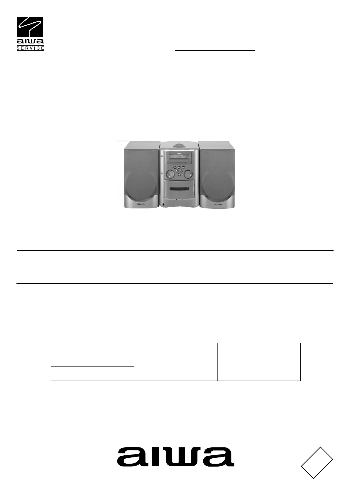
COMPACT DISC STEREO SYSTEM
SYSTEM
XR-M161HS(S)
XR-M161K(S)
CD–CASSEIVER
BASIC CD MECHANISM : DA11T3C (XR-M161HS)
BASIC CD MECHANISM :
CX-SLM161
KSM213CDM (XR-M161K)
SPEAKER
SX-SLM161
S/M Code No. 09-014-355-2N2
DATA
Page 2

TABLE OF CONTENTS
SPECIFICATIONS .............................................................................................................................................. 3
ACCESSORIES/PACKAGE LIST-1/1 ................................................................................................................. 4
PROTECTION OF EYES FROM LASER BEAM DURING SERVICING ............................................................ 5
Precaution to replace Optical block (SF-P101NR, KSS-213C)........................................................................... 6
ELECTRICAL MAIN PARTS LIST ................................................................................................................. 7-12
TRANSISTOR ILLUSTRATION-1/1 .................................................................................................................. 13
WIRING-1/3 (MAIN : K MODEL) ....................................................................................................................... 14
WIRING-2/3 (MAIN : HS MODEL) .................................................................................................................... 15
SCHEMATIC DIAGRAM-1/5 (MAIN 1/2)........................................................................................................... 16
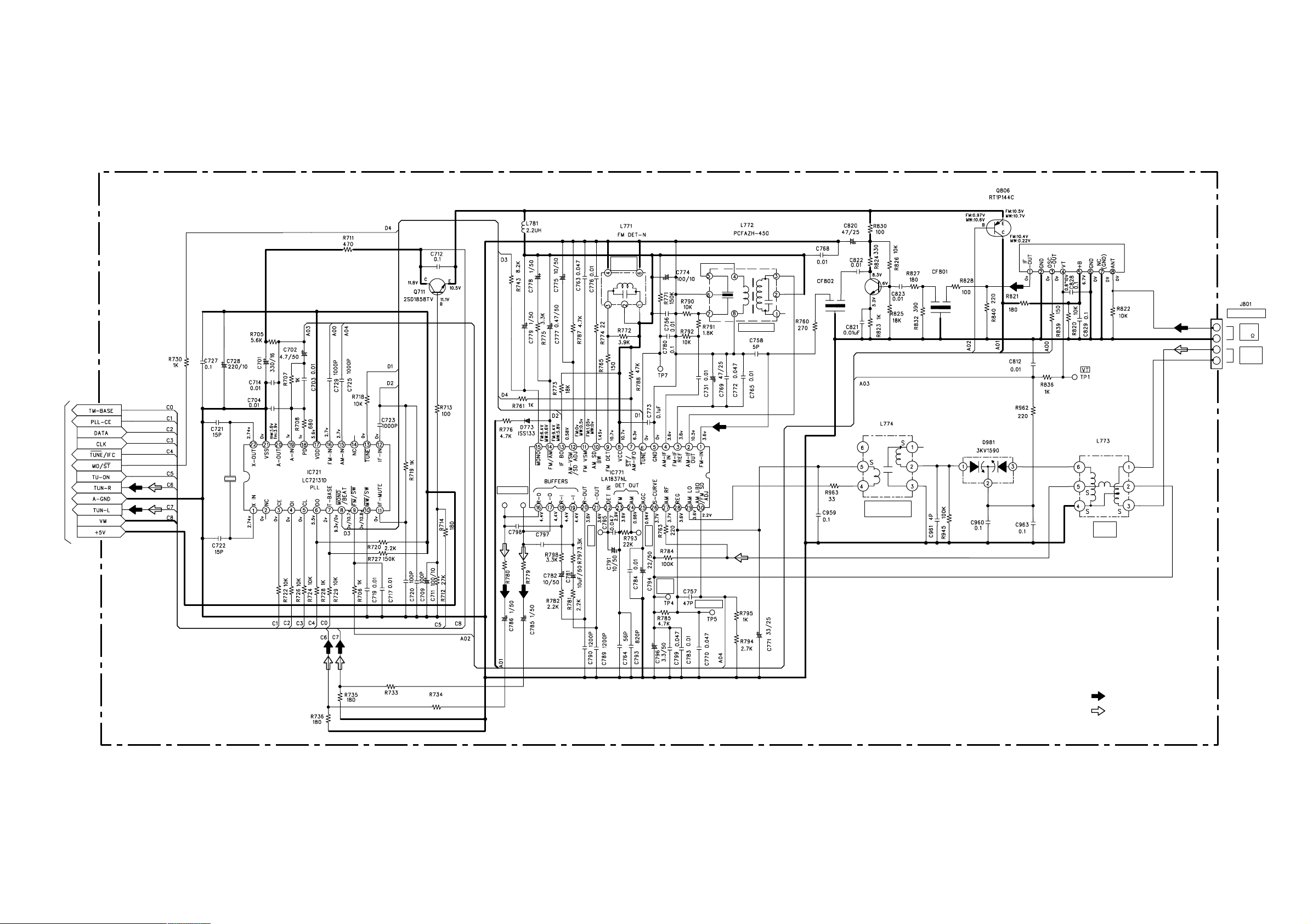
SCHEMATIC DIAGRAM-2/5 (MAIN 2/2 : K MODEL) ....................................................................................... 17
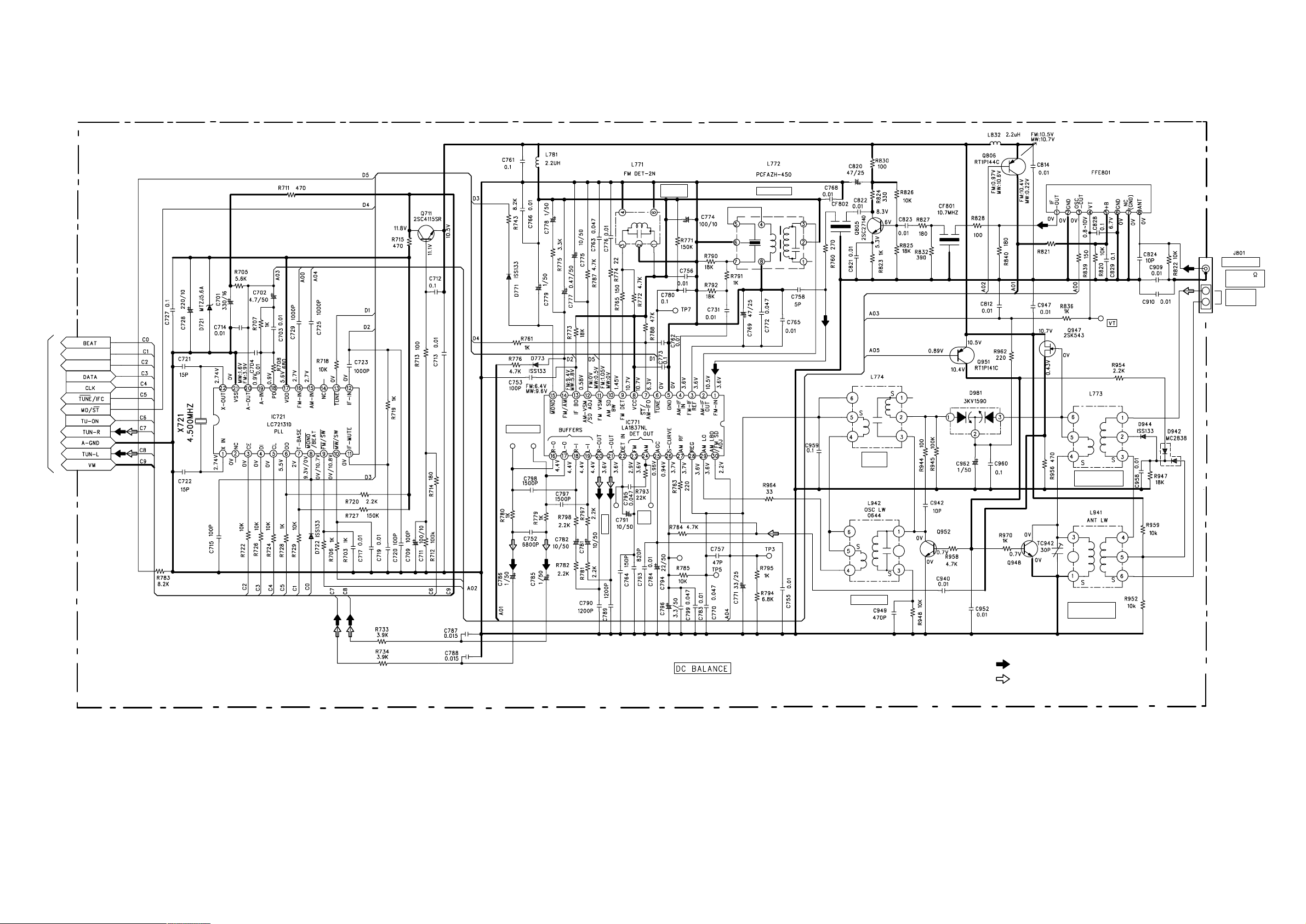
SCHEMATIC DIAGRAM-3/5 (MAIN 2/2 : HS MODEL).....................................................................................18
WIRING-3/3 (FRONT)....................................................................................................................................... 19
SCHEMATIC DIAGRAM-4/5 (FRONT) ............................................................................................................. 20
SCHEMATIC DIAGRAM-5/5 (CD : HS MODEL)............................................................................................... 21
SCHEMATIC DIAGRAM-5/5 (CD : K MODEL) ............................................................................................... 21a
FL (ZCL-8) GRID ASSIGNMENT/ANODE CONNECTION-1/1......................................................................... 22
ELECTRICAL ADJUSTMENT...................................................................................................................... 23-35
CD TEST MODE ............................................................................................................................................... 36
IC BLOCK DIAGRAM-1/2 ................................................................................................................................. 37
IC BLOCK DIAGRAM-2/2 ................................................................................................................................. 38
IC DISCRIPTION-1/3 (LA9241ML) ............................................................................................................. 39, 40
IC DISCRIPTION-2/3 (LC78622NE) ........................................................................................................... 41, 42
IC DISCRIPTION-3/3 (LC867248A-5V96) .................................................................................................. 43, 44
MECHANICAL EXPLODED VIEW-1/1.............................................................................................................. 45
MECHANICAL PARTS LIST-1/1................................................................................................................. 46, 47
TAPE MECHANISM EXPLODED VIEW-1/1 (2ZM-1 YR12NC)........................................................................ 48
TAPE MECHANISM PARTS LIST-1/1 (2ZM-1 YR12NC) ................................................................................. 49
CD MECHANISM EXPLODED VIEW-1/2 (DA-11T3C)..................................................................................... 50
CD MECHANISM PARTS LIST-1/2 (DA-11T3C).............................................................................................. 51
CD MECHANISM EXPLODED VIEW-2/2 (KSM-213CDM) .............................................................................. 52
CD MECHANISM PARTS LIST-2/2 (KSM-213CDM)........................................................................................53
SPEAKER DISASSEMBLY INSTRUCTIONS-1/1............................................................................................. 54
SPEAKER PARTS LIST-1/1 ............................................................................................................................. 55
-2-
Page 3
(K MODEL)
SPECIFICATIONS
Design and specifications are subject to change without
•
notice
.
(HS MODEL)
Design and specifications are subject to change without
•
notice
.
-3-
Page 4

ACCESSORIES/PACKAGE LIST-1/1
REF. NO PART NO. KANRI DESCRIPTION
1 8B-CLA-931-010 IB,HS(K)B<161HSSC>
1 8B-CLB-905-110 IB,K(E)B<161KSC>
2 8A-CLB-961-110 RC UNIT,RC-AAT11
3 87-A90-030-010 ANT,LOOP AM-NC C
4 87-043-115-010 ANT,FEEDER FM<161HSSC>
5 87-A90-118-010 ANT,WIRE FM (Z)<161KSC>
!
6 87-099-726-010 PLUG,ADPTR CONV(K)<161KSC>
!
7 87-A91-017-010 PLUG,CONVERSION JT-0476<161HSSC>
NO.
-4-
Page 5
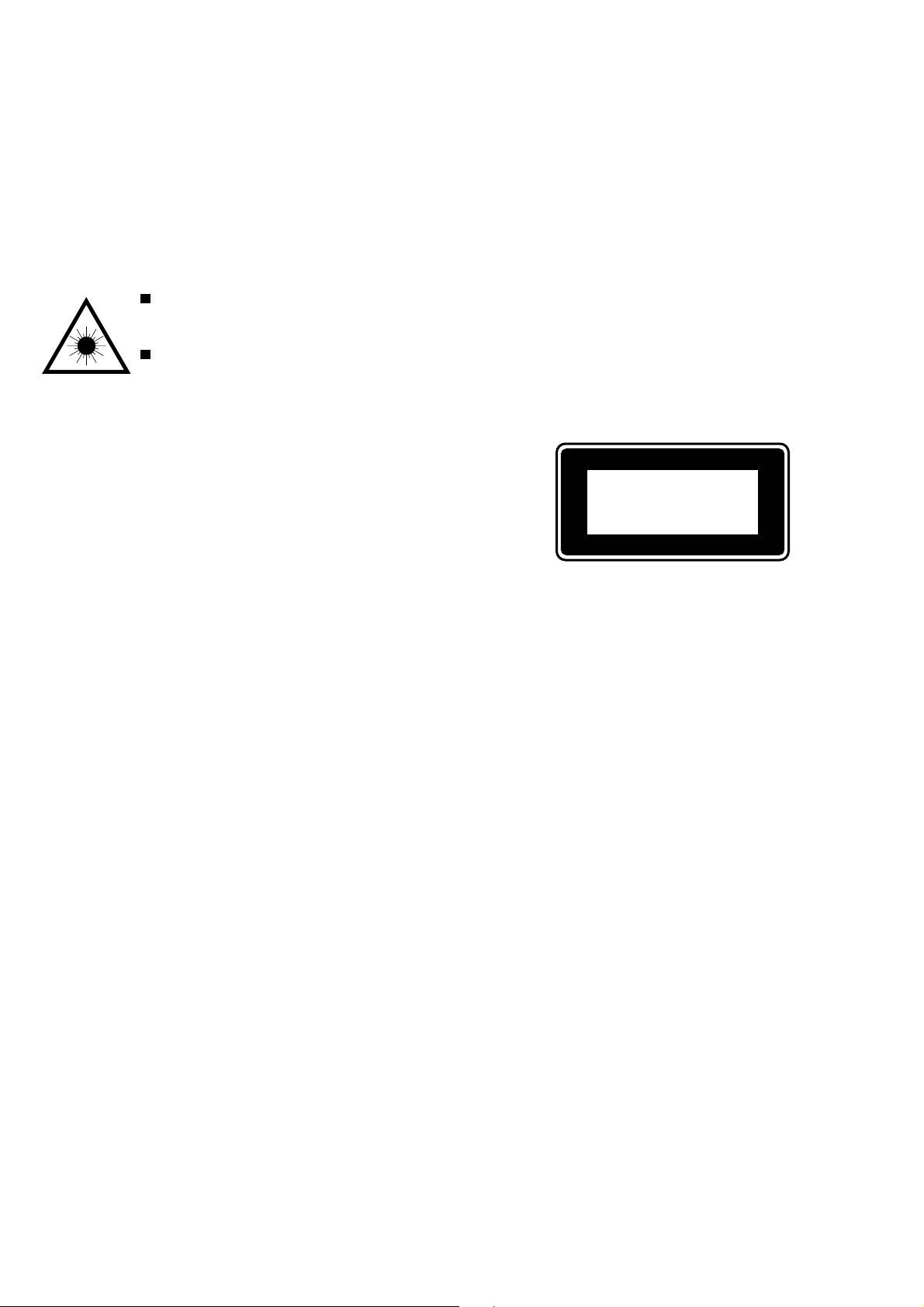
PROTECTION OF EYES FROM LASER BEAM DURING SERVICING
This set employs laser. Therefore, be sure to follow carefully the
instructions below when servicing.
WARNING!
WHEN SERVICING, DO NOT APPROACH THE LASER EXIT
WITH THE EYE TOO CLOSELY. IN CASE IT IS NECESSARY TO
CONFIRM LASER BEAM EMISSION. BE SURE TO OBSERVE
FROM A DISTANCE OF MORE THAN 30cm FROM THE
SURFACE OF THE OBJECTIVE LENS ON THE OPTICAL
PICK-UP BLOCK.
Caution: Invisible laser radiation when
open and interlocks defeated avoid exposure to beam.
Advarsel:Usynling laserståling ved åbning,
når sikkerhedsafbrydere er ude af funktion.
Undgå udsættelse for stråling.
VAROITUS!
Laiteen Käyttäminen muulla kuin tässä käyttöohjeessa mainitulla tavalla saattaa altistaa käyt-täjän turvallisuusluokan 1 ylittävälle näkymättömälle lasersäteilylle.
VARNING!
Om apparaten används på annat sätt än vad som specificeras i
denna bruksanvising, kan användaren utsättas för osynling
laserstrålning, som överskrider gränsen för laserklass 1.
CAUTION
Use of controls or adjustments or performance of procedures
other than those specified herein may result in hazardous
radiation exposure.
ATTENTION
L'utilisation de commandes, réglages ou procédures autres que
ceux spécifiés peut entraîner une dangereuse exposition aux
radiations.
ADVARSEL!
Usynlig laserståling ved åbning, når sikkerhedsafbrydereer ude
af funktion. Undgå udsættelse for stråling.
This Compact Disc player is classified as a CLASS 1 LASER
product.
The CLASS 1 LASER PRODUCT label is located on the rear
exterior.
CLASS 1
KLASSE 1
LUOKAN 1
KLASS 1
LASER PRODUCT
LASER PRODUKT
LASER LAITE
LASER APPARAT
-5-
Page 6
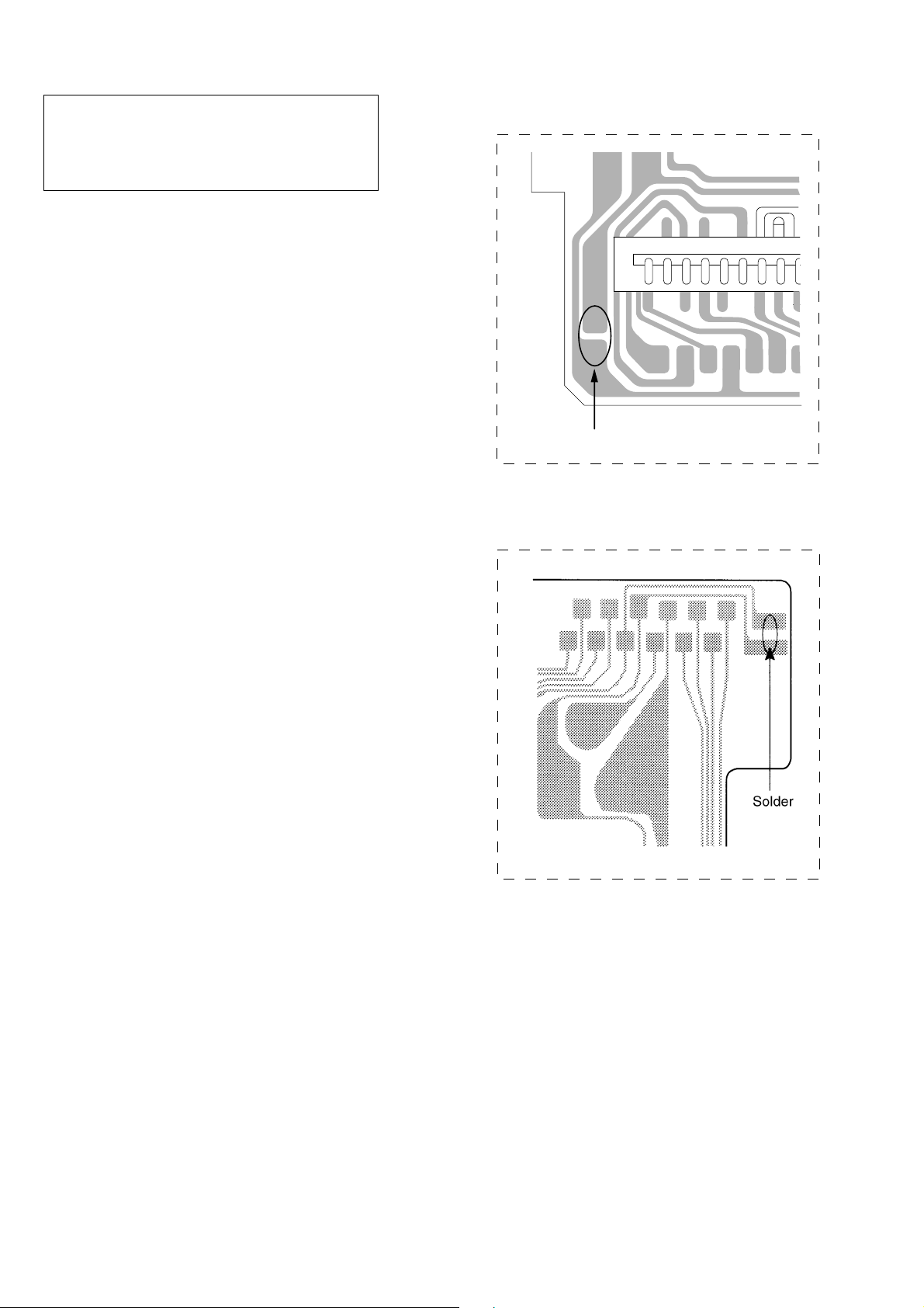
Precaution to replace Optical block
(SF-P101NR, KSS-213C)
Body or clothes electrostatic potential could ruin
laser diode in the optical block. Be sure ground
body and workbench, and use care the clothes
do not touch the diode.
1) After the connection, remove solder shown in
the right figure.
PICK-UP Assy PWB
(SF-P101NR)
Solder
PICK-UP Assy PWB
(KSS-213C)
-6-
Page 7

ELECTRICAL MAIN PARTS LIST-1/6
REF. NO PART NO. KANRI DESCRIPTION
NO.
IC
87-A21-756-010 IC,LA4629
87-A21-443-040 C-IC,M62495AFP
8B-CLA-630-010 IC,LC867248A-5V96
87-A21-245-010 IC,RPM6938-V4
87-A21-145-040 IC BA4560F For 2 CH OPE. AMP
87-A20-446-010 C-IC,LA9241ML
87-A21-319-010 C-IC,LC78622NE
87-A21-093-010 IC,LA6541D
87-A21-928-010 IC LC72131D (Z) [SANYO]
87-A20-913-010 IC,LA1837NL
TRANSISTOR
87-026-610-080 TR,KTC3198GR
87-A30-476-010 TR,KTA1046Y
87-A30-185-010 TR,2SD1381F
87-026-313-080 TR,DTC343TS
87-CD7-603-080 TR,SS8050
87-A30-432-040 C-TR,DTC124XK (0.2W)
86-NFZ-664-080 C-TR,DTC143TK
89-320-011-080 TR,2SC2001K
S1-911-240-000 TR,2SB1240
89-109-521-080 TR,2SA952K
87-A30-492-080 TR 2SC5343G [AUK] [AIWA]
87-A30-091-080 FET,2SJ460
87-026-218-080 TR,DTC144ES
87-A30-151-080 TR,2SA1993F
89-333-317-010 TR,2SC3331TU
89-109-332-380 TR,2SA933S-S (300mw)
87-A30-515-080 TR,2SA1979O/Y
87-A30-287-040 C-TR DTC114TK (0.2W) [ROHM]
87-026-210-040 C-TR,DTC144EK (200MW)
89-112-965-080 TR,2SA1296GR
87-026-291-080 TR,DTC124XS (0.3W)AI
89-418-580-080 TR,2SD1858TV<161 HSSC>
87-A30-196-080 TR,2SC4115SR (400MW)<161 KSC>
89-327-143-080 C-TR,2SC2714O
87-A30-072-080 C-TR,RT1P 144C
89-505-434-540 C-FET,2SK543(4/5)<161 KSC>
87-A30-257-080 C-TR 2SD1306E (200mw) [CDIL]<161 KSC>
87-A30-074-080 C-TR,RT1P 141C<161 KSC>
DIODE
87-020-465-080 DIODE,1SS133
87-A40-393-090 Diode 1N5402-BD54 [RECTRON]
87-070-334-080 ZENER,MTZJ10B
87-070-335-080 Zener Diode MTZJ8.2B,26mm TAPE
87-017-932-080 ZENER,MTZJ6.2B
87-070-136-080 ZENER,MTZJ5.1B
87-020-027-080 C-DIODE,1SS184
87-A40-442-080 ZENER DIODE MTZJ9.1A 1/2W. AI
87-A40-234-080 ZENER,MTZJ5.6A<161 KSC>
87-A40-270-080 C-DIODE,MC2838<161 KSC>
87-A40-290-080 Vari-Cap. Diode 3KV1590 [MI TY
MAIN C.B<161 HSSC>
C101 87-A12-310-080 C-CAP, U 0.01UF-50V K X7R
C102 87-A12-310-080 C-CAP, U 0.01UF-50V K X7R
C103 87-A12-310-080 C-CAP, U 0.01UF-50V K X7R
C104 87-010-404-080 CAP,E 4.7-50 M 11L SME
C105 87-010-403-080 CAP,E 3.3-50 M 11L SME
C106 87-010-192-080 C-CAP,S 0.022-50 Z F C2012
C107 87-010-192-080 C-CAP,S 0.022-50 Z F C2012
C108 87-010-192-080 C-CAP,S 0.022-50 Z F C2012
C109 87-010-192-080 C-CAP,S 0.022-50 Z F C2012
C110 87-A12-310-080 C-CAP, U 0.01UF-50V K X7R
REF. NO PART NO. KANRI DESCRIPTION
C111 87-016-440-090 CAP,E 4700-35V SME
C112 87-012-140-080 C-CAP,S 470P-50 J CH
C113 87-010-408-080 Cap. 47uF M ELEC. 50V P=5mm
C114 87-A12-310-080 C-CAP, U 0.01UF-50V K X7R
C115 87-010-112-080 CAP,E 100-16 M 11L SME
C116 87-010-101-080 CAP,E 220-16 M SME
C117 87-A12-310-080 C-CAP, U 0.01UF-50V K X7R
C118 87-010-263-080 CAP,E 100-10 M 11L SME
C120 87-010-545-080 CAP,E 0.22-50 M 11L SME
C121 87-010-401-080 CAP,E 1-50 M 11L SME
C122 87-010-401-080 CAP,E 1-50 M 11L SME
C125 87-010-401-080 CAP,E 1-50 M 11L SME
C126 87-010-401-080 CAP,E 1-50 M 11L SME
C129 87-A10-831-090 Elect Cap. 1000uF +/-20% 25V
C130 87-A10-831-090 Elect Cap. 1000uF +/-20% 25V
C131 87-A12-310-080 C-CAP, U 0.01UF-50V K X7R
C132 87-A12-310-080 C-CAP, U 0.01UF-50V K X7R
C133 87-A12-310-080 C-CAP, U 0.01UF-50V K X7R
C134 87-A12-310-080 C-CAP, U 0.01UF-50V K X7R
C135 87-010-405-080 CAP,E 10-50 M 11L SME
C136 87-010-404-080 CAP,E 4.7-50 M 11L SME
C139 87-010-401-080 CAP,E 1-50 M 11L SME
C140 87-010-401-080 CAP,E 1-50 M 11L SME
C141 87-010-405-080 CAP,E 10-50 M 11L SME
C142 87-010-405-080 CAP,E 10-50 M 11L SME
C143 87-010-405-080 CAP,E 10-50 M 11L SME
C144 87-010-405-080 CAP,E 10-50 M 11L SME
C145 87-010-404-080 CAP,E 4.7-50 M 11L SME
C146 87-010-404-080 CAP,E 4.7-50 M 11L SME
C147 87-010-408-080 Cap. 47uF M ELEC. 50V P=5mm
C148 87-010-408-080 Cap. 47uF M ELEC. 50V P=5mm
C151 87-010-545-080 CAP,E 0.22-50 M 11L SME
C152 87-010-545-080 CAP,E 0.22-50 M 11L SME
C153 87-010-545-080 CAP,E 0.22-50 M 11L SME
C154 87-010-545-080 CAP,E 0.22-50 M 11L SME
C158 87-010-263-080 CAP,E 100-10 M 11L SME
C159 87-010-182-080 C-CAP,S 2200P-50 K B C2012
C160 87-A12-310-080 C-CAP, U 0.01UF-50V K X7R
C161 87-010-263-080 CAP,E 100-10 M 11L SME
C162 87-A12-310-080 C-CAP, U 0.01UF-50V K X7R
C166 87-012-368-080 C-CAP, S 0.1UF-50V K X7R
C169 87-A12-310-080 C-CAP, U 0.01UF-50V K X7R
C170 87-010-112-080 CAP,E 100-16 M 11L SME
C171 87-010-384-080 Elect. Cap.100UF +/-20% 25V Pi
C173 87-018-131-080 CAP,TC U 1000P-50 K B UP050
C177 87-010-248-080 CAP,E 220-10 M 11L SME
C303 87-010-180-080 C-CAP,S 1500P-50 K B C2012
C304 87-010-180-080 C-CAP,S 1500P-50 K B C2012
C305 87-010-263-080 CAP,E 100-10 M 11L SME
C306 87-010-263-080 CAP,E 100-10 M 11L SME
C307 87-010-830-080 C-CAP.U 0.068uF-16V K X7R
C308 87-010-830-080 C-CAP.U 0.068uF-16V K X7R
C309 87-010-188-080 C-CAP,S 6800P-50 K B C2012
C310 87-010-188-080 C-CAP,S 6800P-50 K B C2012
C312 87-010-401-080 CAP,E 1-50 M 11L SME
C313 87-010-401-080 CAP,E 1-50 M 11L SME
C314 87-010-401-080 CAP,E 1-50 M 11L SME
C315 87-010-401-080 CAP,E 1-50 M 11L SME
C316 87-010-182-080 C-CAP,S 2200P-50 K B C2012
C317 87-010-182-080 C-CAP,S 2200P-50 K B C2012
C318 87-A12-364-080 Cap. 0.01 uF K Mylar 100V AI
C319 87-A12-364-080 Cap. 0.01 uF K Mylar 100V AI
C320 87-A10-295-080 Cap. 0.01UF J Mylar 50V AI
C321 87-A10-295-080 Cap. 0.01UF J Mylar 50V AI
C322 87-010-321-080 C-CAP,S 82P-50 J CH
C323 87-010-321-080 C-CAP,S 82P-50 J CH
C324 87-010-112-080 CAP,E 100-16 M 11L SME
C325 87-010-112-080 CAP,E 100-16 M 11L SME
C326 87-010-192-080 C-CAP,S 0.022-50 Z F C2012
C327 87-010-183-080 C-CAP,S 2700P-50 K B GRM
NO.
-7-
Page 8

ELECTRICAL MAIN PARTS LIST-2/6
REF. NO PART NO. KANRI DESCRIPTION
NO.
C328 87-010-183-080 C-CAP,S 2700P-50 K B GRM
C329 87-010-183-080 C-CAP,S 2700P-50 K B GRM
C331 87-010-382-080 CAP,E 22-25 M 11L SME
C332 87-010-187-080 C-CAP,S 5600P-50 K B
C333 87-010-178-080 C-CAP,S 1000P-50 K B C2012
C335 87-012-158-080 C-CAP,S 390P-50 J CH GRM
C336 87-012-158-080 C-CAP,S 390P-50 J CH GRM
C337 87-010-192-080 C-CAP,S 0.022-50 Z F C2012
C338 87-012-140-080 C-CAP,S 470P-50 J CH
C339 87-010-405-080 CAP,E 10-50 M 11L SME
C340 87-010-405-080 CAP,E 10-50 M 11L SME
C341 87-010-318-080 C-CAP,S 47P-50 J CH GRM
C342 87-010-318-080 C-CAP,S 47P-50 J CH GRM
C345 87-012-272-080 C-CAP, U 680P-50V K X7R
C346 87-012-272-080 C-CAP, U 680P-50V K X7R
C350 87-010-374-080 CAP,E 47-10 M 11L SME
C351 87-010-234-040 Cap. 47UF M Elec. 16V P=5mm
C354 87-012-268-080 C-CAP, U 330P-50V J C0G
C355 87-012-268-080 C-CAP, U 330P-50V J C0G
C701 87-010-381-080 CAP,E 330-16 M SME
C702 87-010-404-080 CAP,E 4.7-50 M 11L SME
C703 87-A12-310-080 C-CAP, U 0.01UF-50V K X7R
C704 87-A12-310-080 C-CAP, U 0.01UF-50V K X7R
C709 87-012-195-080 C-CAP,U 100P-50 J CH
C711 87-010-263-080 CAP,E 100-10 M 11L SME
C712 87-010-196-080 C-CAP,S 0.1-25 Z F C2012
C714 87-A12-310-080 C-CAP, U 0.01UF-50V K X7R
C717 87-A12-310-080 C-CAP, U 0.01UF-50V K X7R
C719 87-A12-310-080 C-CAP, U 0.01UF-50V K X7R
C720 87-012-195-080 C-CAP,U 100P-50 J CH
C721 87-012-176-080 C-CAP,U 15P-50 J CH
C722 87-012-176-080 C-CAP,U 15P-50 J CH
C723 87-012-274-080 C-CAP,U 1000P-50 K B
C725 87-012-274-080 C-CAP,U 1000P-50 K B
C727 87-010-196-080 C-CAP,S 0.1-25 Z F C2012
C728 87-010-248-080 CAP,E 220-10 M 11L SME
C729 87-012-274-080 C-CAP,U 1000P-50 K B
C731 87-A12-310-080 C-CAP, U 0.01UF-50V K X7R
C756 87-A12-310-080 C-CAP, U 0.01UF-50V K X7R
C757 87-012-188-080 C-CAP,U 47P-50 J CH
C758 87-012-167-080 C-CAP,U 5P-50 C CH
C763 87-010-596-080 CAP,S 0.047-16
C764 87-012-337-080 C-CAP,U 56P-50 J CH GRM
C765 87-A12-310-080 C-CAP, U 0.01UF-50V K X7R
C768 87-A12-310-080 C-CAP, U 0.01UF-50V K X7R
C769 87-010-260-080 CAP,E 47-25 M 11L SME
C770 87-010-596-080 CAP,S 0.047-16
C771 87-010-383-080 CAP,E 33-25 M 11L SME
C772 87-010-596-080 CAP,S 0.047-16
C773 87-010-196-080 C-CAP,S 0.1-25 Z F C2012
C774 87-010-263-080 CAP,E 100-10 M 11L SME
C775 87-010-405-080 CAP,E 10-50 M 11L SME
C776 87-A12-310-080 C-CAP, U 0.01UF-50V K X7R
C777 87-010-400-080 CAP,E 0.47-50 M 11L SME
C778 87-010-401-080 CAP,E 1-50 M 11L SME
C779 87-010-401-080 CAP,E 1-50 M 11L SME
C780 87-010-196-080 C-CAP,S 0.1-25 Z F C2012
C781 87-010-405-080 CAP,E 10-50 M 11L SME
C782 87-010-405-080 CAP,E 10-50 M 11L SME
C783 87-A12-310-080 C-CAP, U 0.01UF-50V K X7R
C784 87-A12-310-080 C-CAP, U 0.01UF-50V K X7R
C785 87-010-401-080 CAP,E 1-50 M 11L SME
C786 87-010-401-080 CAP,E 1-50 M 11L SME
C789 87-012-275-080 C-CAP,U 1200P-50 K B GRM
C790 87-012-275-080 C-CAP,U 1200P-50 K B GRM
C791 87-010-405-080 CAP,E 10-50 M 11L SME
C793 87-012-273-080 C-CAP,U 820P-50 K B
C794 87-010-406-080 CAP,E 22-50 M 11L SME
C795 87-010-596-080 CAP,S 0.047-16
C796 87-010-403-080 CAP,E 3.3-50 M 11L SME
REF. NO PART NO. KANRI DESCRIPTION
C797 87-012-276-080 C-CAP,U 1500P-50 K B
C798 87-012-276-080 C-CAP,U 1500P-50 K B
C799 87-010-596-080 CAP,S 0.047-16
C812 87-A12-310-080 C-CAP, U 0.01UF-50V K X7R
C820 87-010-260-080 CAP,E 47-25 M 11L SME
C821 87-A12-310-080 C-CAP, U 0.01UF-50V K X7R
C822 87-A12-310-080 C-CAP, U 0.01UF-50V K X7R
C823 87-A12-310-080 C-CAP, U 0.01UF-50V K X7R
C828 87-010-196-080 C-CAP,S 0.1-25 Z F C2012
C829 87-010-196-080 C-CAP,S 0.1-25 Z F C2012
C959 87-010-196-080 C-CAP,S 0.1-25 Z F C2012
C960 87-010-196-080 C-CAP,S 0.1-25 Z F C2012
C961 87-012-166-080 C-CAP, U 4 P-50V C C0G
C963 87-010-196-080 C-CAP,S 0.1-25 Z F C2012
CF801 87-008-261-010 FLTR,CF SFE10.7MA5
CF802 87-008-261-010 FLTR,CF SFE10.7MA5
CN101 88-NF9-658-010 CONN,30P BLK TYK-B(P)
CN301 87-099-832-010 CONN,8P V S2M-8W
!
F101 87-035-457-010 FUSE,3.15A 250V T 218
FC101 87-033-213-080 FUSE CLAMP,PFC5000
FC102 87-033-213-080 FUSE CLAMP,PFC5000
FFE801 A8-8ZA-192-070 8ZA-1 FEUNC ( FM:12V) [AIWA]
J101 8A-CLA-624-010 JACK,PIN 3P AUX
J102 87-A60-754-010 Speaker Terminal 4 pins Push t
J103 87-A60-420-010 Stereo Headphone Jack (DC:34V/
J801 87-A60-202-010 TERMINAL,ANT 4P MSP-154V-02
JW718 87-A50-079-080 COIL,22UH (CECS)
L101 87-005-366-010 COIL,1UH K
L102 87-005-366-010 COIL,1UH K
L104 87-005-676-080 COIL,2.2UH K LF5.0S
L301 87-007-342-010 COIL OSC 85K BIAS
L771 87-A50-266-010 COIL FM DET-N (TOK)
L772 87-A90-733-010 FLTR,PCFAZH-450 (TOK)
L773 S6-046-410-000 AM ANT COIL PIN : 3-1:15T
L774 S6-033-110-000 AM OSC COIL PIN: 1-2:62T
L781 87-005-676-080 COIL,2.2UH K CECS
!
PR100 87-A91-940-080 PROTECTOR,2.5A 20P 60V
R118 SR-F82-000-25N RES,FUSE 82-1/2W J
WH101 87-099-043-010 CONN 2P EH
X721 87-A70-061-010 VIB,XTAL 4.500MHZ CSA-309
MAIN C.B<161 KSC>
C101 87-A12-310-080 C-CAP, U 0.01UF-50V K X7R
C102 87-A12-310-080 C-CAP, U 0.01UF-50V K X7R
C103 87-A12-310-080 C-CAP, U 0.01UF-50V K X7R
C104 87-010-404-080 CAP,E 4.7-50 M 11L SME
C105 87-010-403-080 CAP,E 3.3-50 M 11L SME
C106 87-010-192-080 C-CAP,S 0.022-50 Z F C2012
C107 87-010-192-080 C-CAP,S 0.022-50 Z F C2012
C108 87-010-192-080 C-CAP,S 0.022-50 Z F C2012
C109 87-010-192-080 C-CAP,S 0.022-50 Z F C2012
C110 87-A12-310-080 C-CAP, U 0.01UF-50V K X7R
C111 87-016-440-090 CAP,E 4700-35V SME
C112 87-012-140-080 C-CAP,S 470P-50 J CH
C113 87-010-408-080 Cap. 47uF M ELEC. 50V P=5mm
C114 87-A12-310-080 C-CAP, U 0.01UF-50V K X7R
C115 87-010-112-080 CAP,E 100-16 M 11L SME
C116 87-010-101-080 CAP,E 220-16 M SME
C117 87-A12-310-080 C-CAP, U 0.01UF-50V K X7R
C118 87-010-263-080 CAP,E 100-10 M 11L SME
C120 87-010-545-080 CAP,E 0.22-50 M 11L SME
C121 87-010-401-080 CAP,E 1-50 M 11L SME
C122 87-010-401-080 CAP,E 1-50 M 11L SME
C125 87-010-401-080 CAP,E 1-50 M 11L SME
C126 87-010-401-080 CAP,E 1-50 M 11L SME
C129 87-A10-831-090 Elect Cap. 1000uF +/-20% 25V
C130 87-A10-831-090 Elect Cap. 1000uF +/-20% 25V
NO.
-8-
Page 9

ELECTRICAL MAIN PARTS LIST-3/6
REF. NO PART NO. KANRI DESCRIPTION
NO.
C131 87-A12-310-080 C-CAP, U 0.01UF-50V K X7R
C132 87-A12-310-080 C-CAP, U 0.01UF-50V K X7R
C133 87-A12-310-080 C-CAP, U 0.01UF-50V K X7R
C134 87-A12-310-080 C-CAP, U 0.01UF-50V K X7R
C135 87-010-405-080 CAP,E 10-50 M 11L SME
C136 87-010-404-080 CAP,E 4.7-50 M 11L SME
C139 87-010-401-080 CAP,E 1-50 M 11L SME
C140 87-010-401-080 CAP,E 1-50 M 11L SME
C141 87-010-405-080 CAP,E 10-50 M 11L SME
C142 87-010-405-080 CAP,E 10-50 M 11L SME
C143 87-010-405-080 CAP,E 10-50 M 11L SME
C144 87-010-405-080 CAP,E 10-50 M 11L SME
C145 87-010-404-080 CAP,E 4.7-50 M 11L SME
C146 87-010-404-080 CAP,E 4.7-50 M 11L SME
C147 87-010-408-080 Cap. 47uF M ELEC. 50V P=5mm
C148 87-010-408-080 Cap. 47uF M ELEC. 50V P=5mm
C151 87-010-545-080 CAP,E 0.22-50 M 11L SME
C152 87-010-545-080 CAP,E 0.22-50 M 11L SME
C153 87-010-545-080 CAP,E 0.22-50 M 11L SME
C154 87-010-545-080 CAP,E 0.22-50 M 11L SME
C158 87-010-263-080 CAP,E 100-10 M 11L SME
C159 87-010-182-080 C-CAP,S 2200P-50 K B C2012
C160 87-A12-310-080 C-CAP, U 0.01UF-50V K X7R
C161 87-010-263-080 CAP,E 100-10 M 11L SME
C162 87-A12-310-080 C-CAP, U 0.01UF-50V K X7R
C166 87-012-368-080 C-CAP, S 0.1UF-50V K X7R
C169 87-A12-310-080 C-CAP, U 0.01UF-50V K X7R
C170 87-010-112-080 CAP,E 100-16 M 11L SME
C171 87-010-384-080 Elect. Cap.100UF +/-20% 25V Pi
C173 87-018-131-080 CAP,TC U 1000P-50 K B UP050
C174 87-012-368-080 C-CAP, S 0.1UF-50V K X7R
C175 87-A12-310-080 C-CAP, U 0.01UF-50V K X7R
C176 87-A12-310-080 C-CAP, U 0.01UF-50V K X7R
C177 87-010-248-080 CAP,E 220-10 M 11L SME
C303 87-010-180-080 C-CAP,S 1500P-50 K B C2012
C304 87-010-180-080 C-CAP,S 1500P-50 K B C2012
C305 87-010-263-080 CAP,E 100-10 M 11L SME
C306 87-010-263-080 CAP,E 100-10 M 11L SME
C307 87-010-830-080 C-CAP.U 0.068uF-16V K X7R
C308 87-010-830-080 C-CAP.U 0.068uF-16V K X7R
C309 87-010-188-080 C-CAP,S 6800P-50 K B C2012
C310 87-010-188-080 C-CAP,S 6800P-50 K B C2012
C312 87-010-401-080 CAP,E 1-50 M 11L SME
C313 87-010-401-080 CAP,E 1-50 M 11L SME
C314 87-010-401-080 CAP,E 1-50 M 11L SME
C315 87-010-401-080 CAP,E 1-50 M 11L SME
C316 87-010-182-080 C-CAP,S 2200P-50 K B C2012
C317 87-010-182-080 C-CAP,S 2200P-50 K B C2012
C318 87-A12-364-080 Cap. 0.01 uF K Mylar 100V AI
C319 87-A12-364-080 Cap. 0.01 uF K Mylar 100V AI
C320 87-A10-295-080 Cap. 0.01UF J Mylar 50V AI
C321 87-A10-295-080 Cap. 0.01UF J Mylar 50V AI
C322 87-010-321-080 C-CAP,S 82P-50 J CH
C323 87-010-321-080 C-CAP,S 82P-50 J CH
C324 87-010-112-080 CAP,E 100-16 M 11L SME
C325 87-010-112-080 CAP,E 100-16 M 11L SME
C326 87-010-192-080 C-CAP,S 0.022-50 Z F C2012
C327 87-010-183-080 C-CAP,S 2700P-50 K B GRM
C328 87-010-183-080 C-CAP,S 2700P-50 K B GRM
C329 87-010-183-080 C-CAP,S 2700P-50 K B GRM
C331 87-010-382-080 CAP,E 22-25 M 11L SME
C332 87-010-187-080 C-CAP,S 5600P-50 K B
C333 87-010-178-080 C-CAP,S 1000P-50 K B C2012
C335 87-012-158-080 C-CAP,S 390P-50 J CH GRM
C336 87-012-158-080 C-CAP,S 390P-50 J CH GRM
C337 87-010-192-080 C-CAP,S 0.022-50 Z F C2012
C338 87-012-140-080 C-CAP,S 470P-50 J CH
C339 87-010-405-080 CAP,E 10-50 M 11L SME
C340 87-010-405-080 CAP,E 10-50 M 11L SME
C341 87-010-318-080 C-CAP,S 47P-50 J CH GRM
REF. NO PART NO. KANRI DESCRIPTION
NO.
C342 87-010-318-080 C-CAP,S 47P-50 J CH GRM
C345 87-012-272-080 C-CAP, U 680P-50V K X7R
C346 87-012-272-080 C-CAP, U 680P-50V K X7R
C350 87-010-374-080 CAP,E 47-10 M 11L SME
C351 87-010-234-040 Cap. 47UF M Elec. 16V P=5mm
C354 87-012-268-080 C-CAP, U 330P-50V J C0G
C355 87-012-268-080 C-CAP, U 330P-50V J C0G
C701 87-010-381-080 CAP,E 330-16 M SME
C702 87-010-404-080 CAP,E 4.7-50 M 11L SME
C703 87-A12-310-080 C-CAP, U 0.01UF-50V K X7R
C704 87-A12-310-080 C-CAP, U 0.01UF-50V K X7R
C709 87-012-195-080 C-CAP,U 100P-50 J CH
C711 87-010-263-080 CAP,E 100-10 M 11L SME
C712 87-010-831-080 C-CAP,U 0.1-16 Z F
C713 87-A12-310-080 C-CAP, U 0.01UF-50V K X7R
C714 87-A12-310-080 C-CAP, U 0.01UF-50V K X7R
C715 87-012-195-080 C-CAP,U 100P-50 J CH
C717 87-A12-310-080 C-CAP, U 0.01UF-50V K X7R
C719 87-A12-310-080 C-CAP, U 0.01UF-50V K X7R
C720 87-012-195-080 C-CAP,U 100P-50 J CH
C721 87-012-176-080 C-CAP,U 15P-50 J CH
C722 87-012-176-080 C-CAP,U 15P-50 J CH
C723 87-012-274-080 C-CAP,U 1000P-50 K B
C725 87-018-131-080 CAP,TC U 1000P-50 K B UP050
C727 87-010-196-080 C-CAP,S 0.1-25 Z F C2012
C728 87-010-248-080 CAP,E 220-10 M 11L SME
C729 87-012-274-080 C-CAP,U 1000P-50 K B
C731 87-A12-310-080 C-CAP, U 0.01UF-50V K X7R
C752 87-012-284-080 C-CAP,U 6800P-50 K B GRM
C753 87-012-195-080 C-CAP,U 100P-50 J CH
C755 87-A12-310-080 C-CAP, U 0.01UF-50V K X7R
C756 87-A12-310-080 C-CAP, U 0.01UF-50V K X7R
C757 87-012-188-080 C-CAP,U 47P-50 J CH
C758 87-012-167-080 C-CAP,U 5P-50 C CH
C761 87-010-196-080 C-CAP,S 0.1-25 Z F C2012
C762 87-A12-310-080 C-CAP, U 0.01UF-50V K X7R
C763 87-010-829-080 C-CAP,U 0.047-16 Z F
C764 87-012-337-080 C-CAP, U 150P-50V J C0G
C765 87-A12-310-080 C-CAP, U 0.01UF-50V K X7R
C766 87-A12-310-080 C-CAP, U 0.01UF-50V K X7R
C768 87-A12-310-080 C-CAP, U 0.01UF-50V K X7R
C769 87-010-260-080 CAP,E 47-25 M 11L SME
C770 87-010-829-080 C-CAP,U 0.047-16 Z F
C771 87-010-383-080 CAP,E 33-25 M 11L SME
C772 87-010-829-080 C-CAP,U 0.047-16 Z F
C773 87-010-196-080 C-CAP,S 0.1-25 Z F C2012
C774 87-010-263-080 CAP,E 100-10 M 11L SME
C775 87-010-405-080 CAP,E 10-50 M 11L SME
C776 87-A12-310-080 C-CAP, U 0.01UF-50V K X7R
C777 87-010-400-080 CAP,E 0.47-50 M 11L SME
C778 87-010-401-080 CAP,E 1-50 M 11L SME
C779 87-010-401-080 CAP,E 1-50 M 11L SME
C780 87-010-196-080 C-CAP,S 0.1-25 Z F C2012
C781 87-010-405-080 CAP,E 10-50 M 11L SME
C782 87-010-405-080 CAP,E 10-50 M 11L SME
C783 87-A12-310-080 C-CAP, U 0.01UF-50V K X7R
C784 87-A12-310-080 C-CAP, U 0.01UF-50V K X7R
C785 87-010-401-080 CAP,E 1-50 M 11L SME
C786 87-010-401-080 CAP,E 1-50 M 11L SME
C787 87-012-287-080 C-CAP,U 0.015-25 Z F
C788 87-012-287-080 C-CAP,U 0.015-25 Z F
C789 87-012-275-080 C-CAP,U 1200P-50 K B GRM
C790 87-012-275-080 C-CAP,U 1200P-50 K B GRM
C791 87-010-405-080 CAP,E 10-50 M 11L SME
C793 87-012-273-080 C-CAP, U 820P-50V K X7R
C794 87-010-406-080 CAP,E 22-50 M 11L SME
C795 87-010-596-080 C-CAP,S 0.047-16 K R C2012
C796 87-010-403-080 CAP,E 3.3-50 M 11L SME
C797 87-012-276-080 C-CAP,U 1500P-50 K B
C798 87-012-276-080 C-CAP,U 1500P-50 K B
-9-
Page 10

ELECTRICAL MAIN PARTS LIST-4/6
REF. NO PART NO. KANRI DESCRIPTION
C799 87-010-829-080 C-CAP,U 0.047-16 Z F
C812 87-A12-310-080 C-CAP, U 0.01UF-50V K X7R
C814 87-A12-310-080 C-CAP, U 0.01UF-50V K X7R
C820 87-010-260-080 CAP,E 47-25 M 11L SME
C821 87-A12-310-080 C-CAP, U 0.01UF-50V K X7R
C822 87-A12-310-080 C-CAP, U 0.01UF-50V K X7R
C823 87-A12-310-080 C-CAP, U 0.01UF-50V K X7R
C824 87-012-172-080 C-CAP,U 10P-50 D CH
C828 87-010-196-080 C-CAP,S 0.1-25 Z F C2012
C829 87-010-196-080 C-CAP,S 0.1-25 Z F C2012
C909 87-A12-310-080 C-CAP, U 0.01UF-50V K X7R
C910 87-A12-310-080 C-CAP, U 0.01UF-50V K X7R
C940 87-A12-310-080 C-CAP, U 0.01UF-50V K X7R
C942 87-012-172-080 C-CAP,U 10P-50 D CH
C947 87-A12-310-080 C-CAP, U 0.01UF-50V K X7R
C949 87-A10-039-080 C-CAP,U 470P-50 J CH
C952 87-A12-310-080 C-CAP, U 0.01UF-50V K X7R
C958 87-A12-310-080 C-CAP, U 0.01UF-50V K X7R
C959 87-010-831-080 C-CAP,U 0.1-16 Z F
C960 87-010-196-080 C-CAP,S 0.1-25 Z F C2012
C962 87-010-401-080 CAP,E 1-50 M 11L SME
CF801 87-008-423-010 FLTR,CF SFE10.7MS3G-A
CF802 82-785-747-010 CF MS2 GLY R
CN101 88-NF9-658-010 CONN,30P BLK TYK-B(P)
CN301 87-099-832-010 CONN,8P V S2M-8W
!
F101 87-035-457-010 FUSE,3.15A 250V T 218
FC101 87-033-213-080 FUSE CLAMP,PFC5000
FC102 87-033-213-080 FUSE CLAMP,PFC5000
FFE801 A8-6ZA-19C-170 6ZA-1 YFEENC
J101 8A-CLA-624-010 JACK,PIN 3P AUX
J102 87-A60-754-010 Speaker Terminal 4 pins Push t
J103 87-A60-420-010 Stereo Headphone Jack (DC:34V/
J104 87-099-608-010 DC JACK HEC3800 (500V)
J801 87-A60-880-010 TERMINAL,ANT-PAL 2P MSP-313V-0
L101 87-005-366-010 COIL,1UH K
L102 87-005-366-010 COIL,1UH K
L104 87-005-676-080 COIL,2.2UH K LF5.0S
L301 87-007-342-010 COIL OSC 85K BIAS
L771 87-A50-266-010 COIL,FM DET-2N(TOK)
L772 87-A90-733-010 FLTR,PCFAZH-450 (TOK)
L773 S6-047-410-000 AN ANT COIL PIN:4-5:99T
L774 S6-047-510-000 AM OSC COIL PIN:5-4:21T
L781 87-005-847-080 COIL,2.2UH K CECS
L832 87-005-847-080 COIL,2.2UH K CECS
L941 87-A50-020-010 COIL,ANT LW (COI) 252KHZ
L942 87-A50-019-010 COIL,OSC LW (COI) 856KHZ
!
PR100 87-A91-940-080 PROTECTOR,2.5A 20P 60V
R118 SR-F82-000-25N RES,FUSE 82-1/2W J
TC942 87-011-164-010 TRIMMER,CER 30P 4.5X3.9 VCT31
WH101 87-099-043-010 CONN 2P EH
X721 87-A70-061-010 VIB,XTAL 4.500MHZ CSA-309
FRONT C.B
C201 87-010-375-080 CAP,E 330-10 M 11L SME
C202 87-010-805-080 C-CAP.S 1uF-16V Z CER.Y5V
C203 87-A12-310-080 C-CAP, U 0.01UF-50V K X7R
C204 87-A12-310-080 C-CAP, U 0.01UF-50V K X7R
C205 87-012-156-080 C-CAP,S 220P-50 J CH GRM
C206 87-A12-310-080 C-CAP, U 0.01UF-50V K X7R
C207 87-A12-310-080 C-CAP, U 0.01UF-50V K X7R
C208 87-010-196-080 C-CAP,S 0.1-25 Z F C2012
C210 87-010-196-080 C-CAP,S 0.1-25 Z F C2012
C211 87-010-314-080 C-CAP,S 22P-50V
C212 87-010-321-080 C-CAP,S 82P-50 J CH
C213 87-012-168-080 C-CAP U 6 P-50V C CER. COG
C214 87-010-314-080 C-CAP,S 22P-50V
C215 87-012-176-080 C-CAP,U 15P-50 J CH
C216 87-010-400-080 CAP,E 0.47-50 M 11L SME
NO.
REF. NO PART NO. KANRI DESCRIPTION
NO.
C217 87-010-196-080 C-CAP,S 0.1-25 Z F C2012
C218 87-010-405-080 CAP,E 10-50 M 11L SME
CN201 87-099-720-010 CONN,30P BLK TYK-B(P)
CN202 87-A60-404-010 CONN,3P TKX-P03P-F1
FB201 87-A90-562-010 F-BCAD 843556 TB36 TAPING 52mm
L201 87-005-676-080 COIL,2.2UH K LF5.0S
L202 87-A50-083-080 COIL,47UH (CECS)
LCD201 8Z-CL8-665-110 LCD,ZCL-8
S200 87-A90-095-080 SW,TACT EVQ11G04M
S201 87-A90-095-080 SW,TACT EVQ11G04M
S202 87-A90-095-080 SW,TACT EVQ11G04M
S203 87-A90-095-080 SW,TACT EVQ11G04M
S204 87-A90-095-080 SW,TACT EVQ11G04M
S205 87-A90-095-080 SW,TACT EVQ11G04M
S206 87-A90-095-080 SW,TACT EVQ11G04M
S207 87-A90-095-080 SW,TACT EVQ11G04M
S208 87-A90-095-080 SW,TACT EVQ11G04M
S209 87-A90-095-080 SW,TACT EVQ11G04M
S213 87-A90-095-080 SW,TACT EVQ11G04M
S214 87-A90-095-080 SW,TACT EVQ11G04M
S215 87-A90-095-080 SW,TACT EVQ11G04M
S216 87-A90-095-080 SW,TACT EVQ11G04M
S217 87-A90-095-080 SW,TACT EVQ11G04M
S218 87-A90-095-080 SW,TACT EVQ11G04M
S219 87-A90-095-080 SW,TACT EVQ11G04M
X201 87-030-364-010 VIB,XTAL 32.768K CT
X202 87-030-376-080 VIB,CER 5.760MHZ CSA MG200
CD C.B
C401 87-010-403-080 CAP,E 3.3-50 M 11L SME
C402 87-010-197-080 C-CAP,S 0.01-25 K B C2012
C403 87-010-263-080 CAP,E 100-10 M 11L SME
C404 87-010-248-080 CAP,E 220-10 M 11L SME
C405 87-010-197-080 C-CAP,S 0.01-25 K B C2012
C406 87-010-374-080 CAP,E 47-10 M 11L SME
C407 87-010-178-080 C-CAP,S 1000P-50 K B C2012
C408 87-010-198-080 C-CAP,S 0.022-25 K B C2012
C409 87-010-248-080 CAP,E 220-10 M 11L SME
C410 87-010-263-080 CAP,E 100-10 M 11L SME
C411 87-A11-177-080 C-CAP,S 0.15-16 K B
C412 87-010-401-080 CAP,E 1-50 M 11L SME
C413 87-016-369-080 C-CAP,S 0.033-25 K B GRM
C414 87-010-405-080 CAP,E 10-50 M 11L SME
C415 87-012-368-080 C-CAP, S 0.1UF-50V K X7R
C416 87-010-545-080 CAP,E 0.22-50 M 11L SME
C417 87-012-157-080 C-CAP,S 330P-50 J CH GRM
C418 87-010-213-080 C-CAP,S 0.015-25 K B GRM
C419 87-A10-201-080 C-CAP,S 0.33-16 K B
C420 87-016-369-080 C-CAP,S 0.033-25 K B GRM
C421 87-A11-177-080 C-CAP,S 0.15-16 K B
C422 87-010-184-080 C-CAP,S 3300P-50 K B C2012<161 HSSC>
C422 87-010-183-080 C-CAP,S 2700P-50 B<161 KSC>
C423 87-010-992-080 C-CAP,S 0.047-25 K B MK212
C424 87-016-460-080 C-CAP,S 0.22-16 K B<161 HSSC>
C424 87-A11-573-080 C-CAP,S 0.018-16 K B<161 KSC>
C425 87-010-176-080 C-CAP,S 680P-50 J SL
C426 87-A10-201-080 C-CAP,S 0.33-16 K B
C428 87-010-197-080 C-CAP,S 0.01-25 K B C2012<161 HSSC>
C428 87-010-426-080 C-CAP,S 0.012-25 B<161 KSC>
C429 87-010-186-080 C-CAP,S 4700P-50 K B C2012
C430 87-012-156-080 C-CAP,S 220P-50 J CH GRM
C431 87-010-545-080 CAP,E 0.22-50 M 11L SME
C432 87-010-374-080 CAP,E 47-10 M 11L SME
C433 87-010-401-080 CAP,E 1-50 M 11L SME
C434 87-010-184-080 C-CAP,S 3300P-50 K B C2012
C435 87-010-197-080 C-CAP,S 0.01-25 K B C2012
C436 87-010-374-080 CAP,E 47-10 M 11L SME
C437 87-010-404-080 CAP,E 4.7-50 M 11L SME
C438 87-012-368-080 C-CAP, S 0.1UF-50V K X7R
-10-
Page 11

ELECTRICAL MAIN PARTS LIST-5/6
REF. NO PART NO. KANRI DESCRIPTION
C439 87-010-178-080 C-CAP,S 1000P-50 K B C2012
C441 87-010-197-080 C-CAP,S 0.01-25 K B C2012
C442 87-010-313-080 C-CAP,S 18P-50 J CH GRM<161 HSSC>
C442 87-010-311-080 C-CAP,S 12P-50 J CH<161 KSC>
C445 87-010-196-080 C-CAP,S 0.1-25 Z F C2012
C446 87-010-196-080 C-CAP,S 0.1-25 Z F C2012
C447 87-010-196-080 C-CAP,S 0.1-25 Z F C2012
C448 87-010-322-080 C-CAP,S 100P-50 J CH GRM
C450 87-012-140-080 C-CAP,S 470P-50 J CH
C451 87-012-156-080 C-CAP,S 220P-50 J CH GRM
C455 87-010-247-080 CAP,E 100-50 M SME
C457 87-010-312-080 C-CAP,S 15P-50 J CH GRM
C458 87-010-312-080 C-CAP,S 15P-50 J CH GRM
C459 87-010-263-080 CAP,E 100-10 M 11L SME
C460 87-015-819-080 C-CAP, 0.01-50 K B C3216
C461 87-010-197-080 C-CAP,S 0.01-25 K B C2012
C462 87-010-248-080 CAP,E 220-10 M 11L SME
C463 87-012-348-080 Cap. 0.1uF Z CER. 50V F TYPE
C464 87-010-263-080 CAP,E 100-10 M 11L SME
C465 87-010-404-080 CAP,E 4.7-50 M 11L SME
C466 87-010-196-080 C-CAP,S 0.1-25 Z F C2012
C467 87-010-263-080 CAP,E 100-10 M 11L SME
C469 87-012-154-080 C-CAP,S 150P-50 J CH GRM
C470 87-010-544-080 CAP,E 0.1-50 M 11L SME
C471 87-015-785-080 C-CAP, 0.1-25 Z F C3216
C472 87-015-785-080 C-CAP, 0.1-25 Z F C3216
C473 87-015-785-080 C-CAP, 0.1-25 Z F C3216
C474 87-015-785-080 C-CAP, 0.1-25 Z F C3216
C475 87-010-197-080 C-CAP,S 0.01-25 K B C2012
C476 87-010-221-080 CAP,E 470-10 M SME
C477 87-010-197-080 C-CAP,S 0.01-25 K B C2012
C478 87-010-263-080 CAP,E 100-10 M 11L SME
C479 87-010-197-080 C-CAP,S 0.01-25 K B C2012
C480 87-010-221-080 CAP,E 470-10 M SME
C481 87-010-405-080 CAP,E 10-50 M 11L SME
C482 87-010-405-080 CAP,E 10-50 M 11L SME
C489 87-010-196-080 C-CAP,S 0.1-25 Z F C2012
C490 87-010-196-080 C-CAP,S 0.1-25 Z F C2012
C491 87-010-197-080 C-CAP,S 0.01-25 K B C2012
C492 87-010-221-080 CAP,E 470-10 M SME
C494 87-012-348-080 Cap. 0.1uF Z CER. 50V F TYPE
C496 87-010-403-080 CAP,E 3.3-50 M 11L SME
C501 87-010-196-080 C-CAP,S 0.1-25 Z F C2012
C502 87-010-322-080 C-CAP,S 100P-50 J CH GRM
C503 87-010-322-080 C-CAP,S 100P-50 J CH GRM
C504 87-010-322-080 C-CAP,S 100P-50 J CH GRM
C505 87-010-322-080 C-CAP,S 100P-50 J CH GRM
C506 87-010-322-080 C-CAP,S 100P-50 J CH GRM
C510 87-012-368-080 C-CAP, S 0.1UF-50V K X7R
CN401 87-A60-424-010 CONN,16P V TOC-B
NO.
CN402 87-A60-670-010 CONN,6P H 2MM JMT
CN403 87-A60-619-010 CONN,2P V 2MM JMT
CNA203 8A-CLA-621-010 CONN ASSY,9P MOTOR
FFC401 8B-CLB-601-010 FF-CABLE,16P 1.0 130MM
L401 87-003-102-080 COIL,10UH J LAL02
L403 87-A50-087-080 COIL,100UH (CECS)
L404 87-A50-079-080 COIL,22UH (CECS)
SFR430 87-024-437-080 SFR, 100K H NVZ6TLTA AI TAPING
X401 87-A70-046-010 VIB,XTAL 16.934MHZ
LED C.B
D941 87-A40-365-080 LED LAMP Green SLR-342 MGT32
D942 87-A40-365-080 LED LAMP Green SLR-342 MGT32
D943 87-A40-365-080 LED LAMP Green SLR-342 MGT32
D944 87-A40-365-080 LED LAMP Green SLR-342 MGT32
D945 87-A40-365-080 LED LAMP Green SLR-342 MGT32
D946 87-A40-365-080 LED LAMP Green SLR-342 MGT32
D947 87-A40-365-080 LED LAMP Green SLR-342 MGT32
D948 87-A40-365-080 LED LAMP Green SLR-342 MGT32
D949 87-A40-365-080 LED LAMP Green SLR-342 MGT32
AC C.B
!
!
CNA101 8A-CLA-630-010 CONN ASSY,2P PT
!
!
MOTOR C.B<161 KSC>
M2 9X-262-576-910 MOTOR GEAR ASSY<161 KSC>
PIN3 91-564-722-110 PIN CONN,6P<161 KSC>
SW1 91-572-085-120 LEAF SW<161 KSC>
MOTOR C.B<161 HSSC>
M2 S0-M10-A09-700 MOTOR SLED ASSY<161 HSSC>
PIN3 S2-369-750-000 PLUG,6P<161 HSSC>
SW1 S4-S13-A01-600 SW,LEAF<161 HSSC>
DECK C.B
CN1 87-009-352-010 CONN,9P PH H
CRD1 82-ZM1-625-010 RBN-CORD,4P-55
M1 87-045-347-010 MOT,SHU2L 70
SFR1 87-024-581-010 SFR,3.3K DIA6V K0A
SOL1 82-ZM3-627-010 SOL ASSY,27 SO
SW2 87-036-110-010 PUSH SWITCH
SW3 87-036-110-010 PUSH SWITCH
SW4 87-036-110-010 PUSH SWITCH
SW5 87-036-110-010 PUSH SWITCH
SW6 87-A90-248-010 SW,MICRO ESE11SH2CXQ
REF. NO PART NO. KANRI DESCRIPTION
NO.
C219 87-010-197-080 C-CAP,S 0.01-25 K B C2012
C220 87-010-197-080 C-CAP,S 0.01-25 K B C2012
PT101 8B-CLA-602-010 POWER TRANSFORMER EN60065<161 KSC>
PT101 8B-CLA-604-010 POWER TRANSFORMER IEC-65
-11-
Page 12
ELECTRICAL MAIN PARTS LIST-6/6
• Regarding connectors, they are not stocked as they are not the initial order items.
The connectors are available after they are supplied from connector manufacturers upon the order is received.
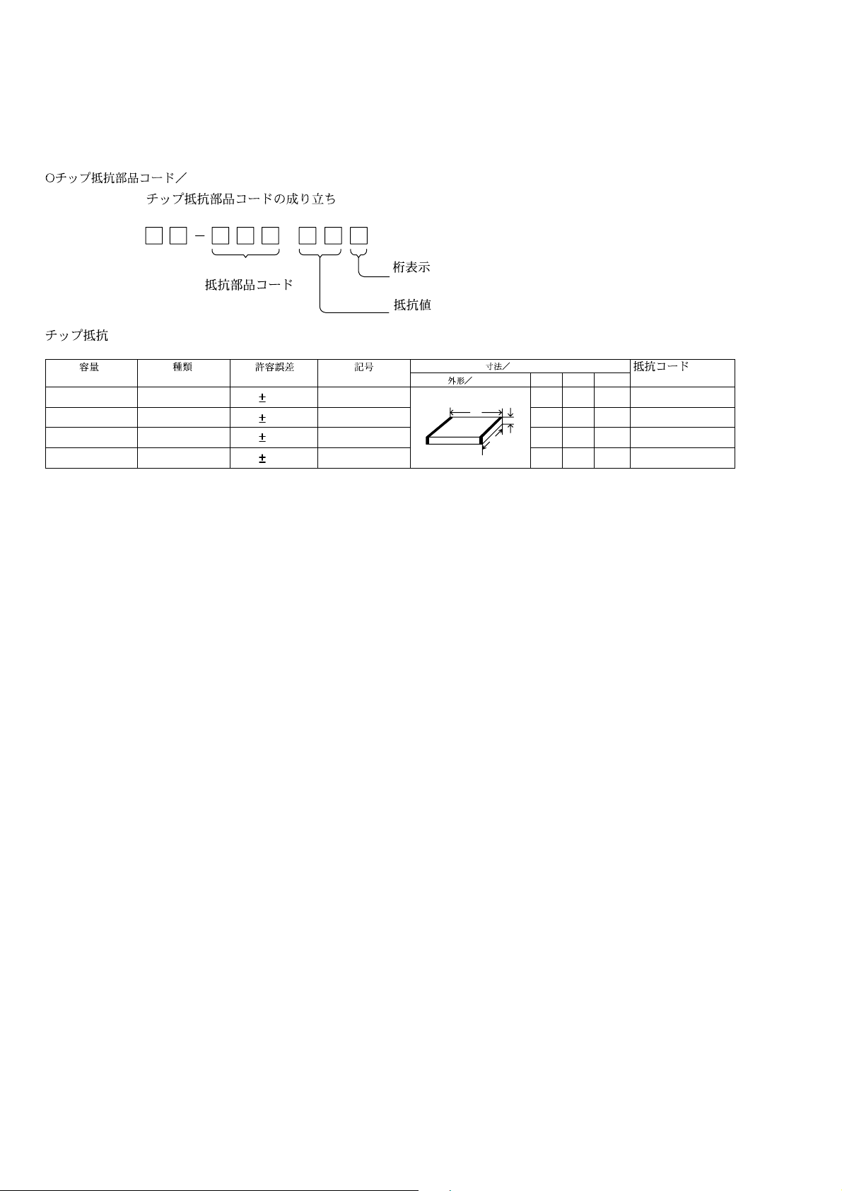
CHIP RESISTOR PART CODE
Chip Resistor Part Coding
88
A
Resistor Code
Chip resistor
Wattage Type Tolerance
1/16W 1005 5% CJ
1/16W
1/10W
1/8W
1608
2125
3216
5%
5%
5%
Symbol
CJ
CJ
CJ
Figure
Value of resistor
Form
L
Dimensions (mm)
t
W
0.55
Resistor Code
108
118
128
LW t
1.0 0.5 0.35 104
1.6 0.8 0.45
2 1.25 0.45
3.2
1.6
: A
: A
-12-
Page 13
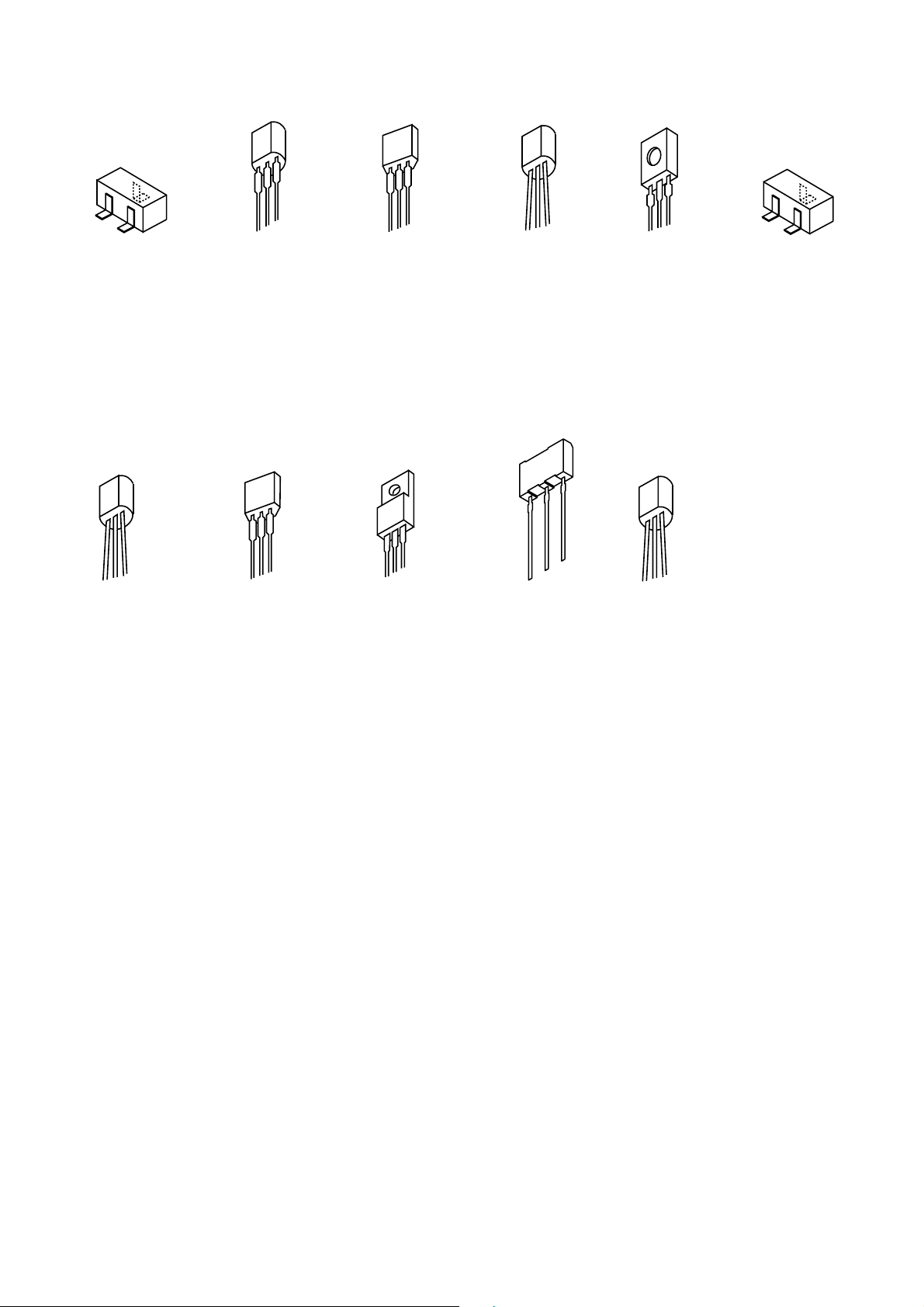
TRANSISTOR ILLUSTRATION-1/1
C
B
E
2SC2714
2SD1306
DTC114TK
DTC143TK
DTC144EK
RT1P141C
PT1P144C
DTC124XK
BCE
ECB ECB ECB ECB
2SA1296
KTC3198
SDG
DTC124XS
DTC343TS
2SA1993F
DTC144ES
2SC3331
BCE
2SA933
2SC2001
2SC4115SR
2SA1979
2SD1858TV
2SA952
ECB
2SD1381
EBC
G
S
D
2SK543
2SC5343G
2SJ460 KTA1046 2SB1240
SS8050
-13-
Page 14
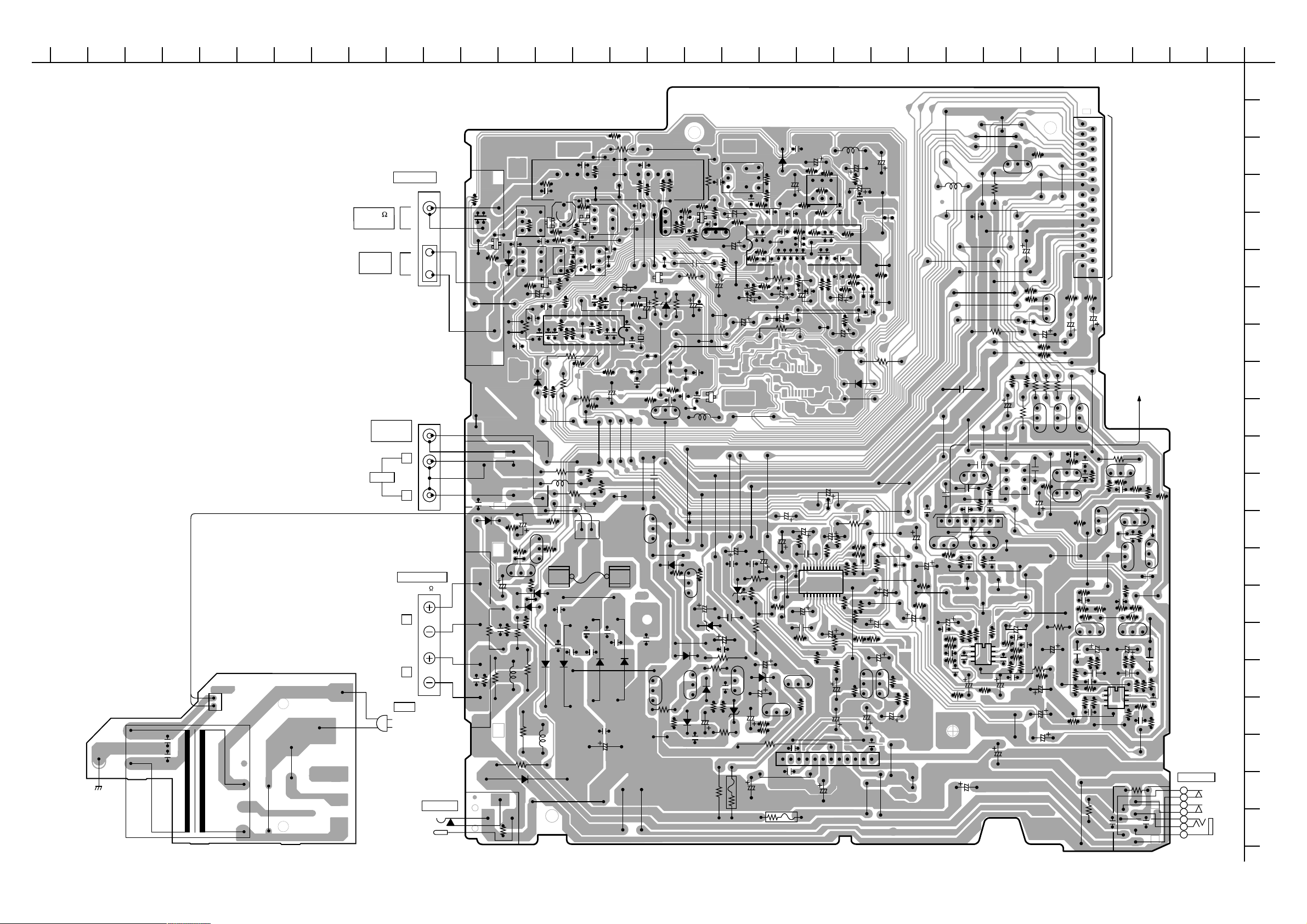
WIRING-1/3 (MAIN : K MODEL)
AC C.B
CNA101
PT101
C220C219
101112131415161718192021222324
1234567892526272829303132
A
MAIN C.B
(K MODEL)
1
CN101
29
R145 R146
C143
R367
ECB
BCE
BCE
R304
R352
C316
R326
R348
Q312
C320
R346R330
R342
R336
2
10
20
TO FRONT C.B CN201
30
C144
TO TAPE MECHANISM
(2ZM-1 YR12NC)
ECB
R362
C328
R356
C327
Q306
R350
BCEBCE
C340
R332
C318
C354
R328
R334
C322
R125
C131
R358
BCE
C317
R327
R344
1
IC301
45
C326
Q311
C319
C338
Q308
R345
8
R335
Q316
BCE
R360
R359
ECB
R351
R349
C339
R329
R343
C323
R126
R363
R325
R333
C132
BCE
R361
Q305
R347
R365
Q307
ECB
C321
R331
C355
R337
J103
PHONES
7
6
5
4
3
2
1
R954
R821
FM 75
(COAXIAL)
MW/LW
LOOP
SUPER
J801
ANTENNA
J101
C910
R959
R947
L941
6
5
C909
4
C958
D942
C960
3
2
D944
1
L773 L774
R956
C962
R719
C715
C829
C824
TC942
B
R962
3
2
1
C717
R726
R956
R706
R722
R970
R728
R958
C942
R945
R727
C949
R948
E
3
2
1
R944
R718
R724
Q952
R720
R714
58
C
C940
C727
IC721
R822
1
Q948
E
C
R952
3
4
5
D981
6
G
D
S
Q947
C723
12 22
C709
C719
C720
D722
R729
B
R712
C952
C729
3
2
1
R708
R733
4
5
6
R820
R707
4
5
6
C703
C711
FFE801
C828
4
1
R828
C812
C
C728
Q951
X721
R839
C712
B
E
B
R715
C
CF801
D721
Q711
R840
C825
B
E
C823
R827
R832
C821
C725
R703
R711
C701
C788
R734
C713
E
L832
R836
L942
C959
C702
R705
C721
C714C704
111
C722
C787
R713
C
R823
R826
CF802
C947
B
C814
E
C768
Q805
Q806
R830
C822
C769
C
L772
3485
2
6
1
7
C765
R792
R824
C820
115
C772
R760
C758
R794
R795
R964
30
R784
C799
C771
R763
C796
C786
WOOFER
R
AUX
R138
L103
L
C160
R127
D108
R101
C104
BCE
D102
R131
R104
R174
R107
R120
Q101
D101
C108
D105
L101
D100
R106
R105
J102
Q102
BCE
SPEAKERS
IMP:4
L
R
2
1
AC~
230V
50Hz
C134
R175
R130
C105
C133
R128
R129
R132
L102
J104
D103
C103
C106
R137
12
F101
C109
C101
R140
WH101
C173
C110
C111
R139
FC102FC101
C102
D106
C107
Q107
D104
D113
Q103
BCE
C166
BCE
C100
R108
R115
R112
D114
Q104
D107
Q106
BCE
BCE
D111
C114
C115
C113
R116
R110
D109
R111
R117
C112
R113
C159
C119
R114
C158
D115
C116
C117
R109
C162
BCE
D110
R118
C160
C118
Q105
C170
DC JACK
R102
C757
R785
R167
R166
R164
C171
R134
C136
C731
R163
R790
C780
C161
D112
R173
R172
C175
PR100
D773
R791
C773
IC771
C756
C762
C783
C770
C755
C794
C785
R743
C139
C153
B
BCE
12 10
C761
C775
64
C774
R771
1
R788
R774
C793
C784
C764
R793
C795
C791
C151
R159
C149
13 24
C152
C150
R160
Q108
CE
R119
Q113
C176
R772
R765
C789
IC102
R787R776
C776
C790
C145
C148
R161
IC101
2
R781
C147
R155
R782
C121
C125
3
C798
C797
C782
C135
L771
C763
C781
112
R150
L781
C779
C753
R733
R798
D771
R153
R149
R142
R158
R121
R775
C777
C766
16
R779
R780
C752
R797
R157
R141
R147
R143
R144
R154 R156
Q109
BCE
R123
C126
C140
Q110
C174
1
R783
R761
C146
R148
C154
BCE
C122
C778
R162
R124
R371
C142
L104
C169
C164
C332
Q313
BCE
C333
R353
C334
C335
C337
CN301
18
Q310
BCE
C306
C346
R312
R320
R308
C129
BCE
C304
C319
R306
R318
1
IC302
45
C342
C312
R311
C303
8
C141
C350
R122
R372
C308
R342
R316
R314
C310
R310
R176
Q309
R305
R309
C313
C351
R354
C336
R317
C341
E
R168
C309
C130
Q111
CB
R369
R338
L301
R169
C120
R135
Q319
R178
ECB
C177
R177
R370
R366
R300
R368
ECB
Q300 Q318 Q317
C329
R357
C330
R355
C331
R339
C305
C345
C307
R307
R315
C325
R313
R340
C324
C314
C315
Q315
Q314
B
C
D
E
F
G
H
I
J
K
L
M
N
O
P
Q
R
S
T
U
-14-
Page 15
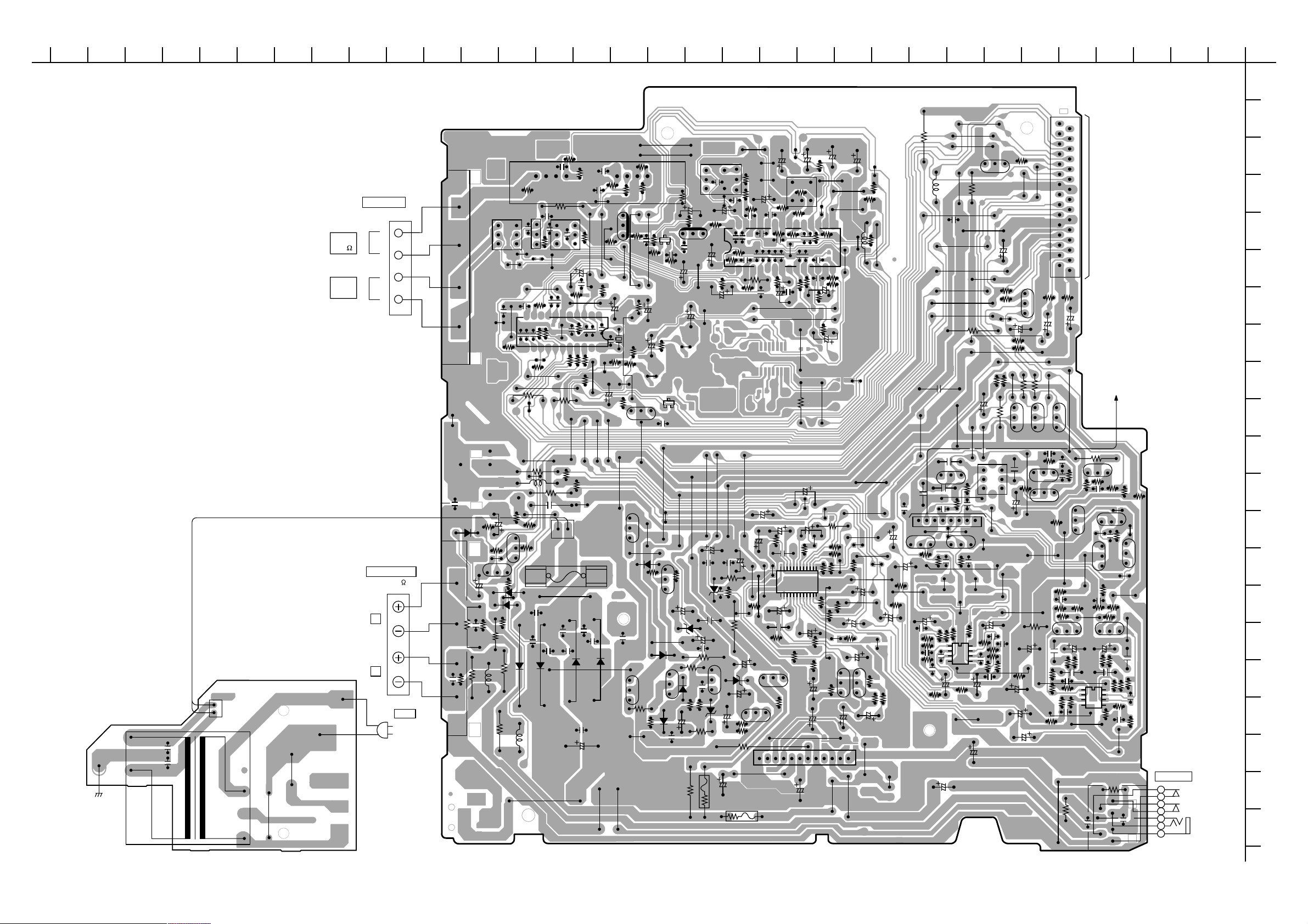
WIRING-2/3 (MAIN : HS MODEL)
AC C.B
2
1
CNA101
PT101
C220C219
FM
75
AM
LOOP
J801
ANTENNA
J102
SPEAKERS
IMP : 4
L
R
AC~
220V
60Hz
MAIN C.B
(HS MODEL)
8
R822
C963
L773
C960
4
3
3
5
2
2
6
1
1
D981
R945
R718
C723
C709
C719
C717
C720
11 1
R719
R728
R138
L103
C134
C160
D100
R175
R130
Q102
C105
C133
R106
R105
BCE
R129
R132
R128
R127
L102
C173
C104
R133
Q101
R107
BCE
R120
FC101 FC102
R104
D101
C103
D102
R131
C108
R174
D105
L101
R821
C829
R962
L774
3
C959
C961
2
1
C725
IC721
R720
R727
R706
R714
R137
12
F101
C109
C106 C101
D103
5
C729
C727
R707
R708
R724
4
5
6
C702
C703
R140
WH101
C110
C111
C812
C704
R726
R820
R963
C714
R712
R139
C107
C102
D106
FFE801
C828
2212
C721
R722
R836
R832
C711
R705
X721
R735
D104
4
CF801
C722
R713
C166
R728
R733
BBCCE
Q107
D113
Q103
R108
R827
R839
R711
R736
Q711
BCEBCE
1
C823
R115
R112
R840
R828
R825
Q805
R826
B
C701
C786
C712
D114
Q106
D107
C820
C
C821
R823
R734
Q104
CF802
E
Q806
E
BCE
D111
C114
C115
BCE
C113
R116
R109
R110
R117
R830
C822
C771
D109
R111
R824
C112
R113
C775
L772
4
3
5
C768
2
6
R790
78
C774
R791
R792
C765
115
C731
C758
C772
C780
R794
C757
C770
R785
R763
C139
C162
C161
R166
R164
C160
R163
C118
D112
Q105
C171
Q113
D110
BCE
C170
R173
R172
R134
12 10
C136
PR100
C785
C159
R114
C794
D115
C119
C116
1
C769
R760
IC771
R795
R784
C796
C158
R167
C117
BCE
R118
R771
C773
R788
C756
C764
C784
C783
R793
C799
C791
C151
C153
C149
13 24
C152
C150
R160
Q108
BCE
R119
C793
C795
R159
1
R774
R161
L771
R772
IC102
C135
23
C789
R781
C145
C147
R155
C148
IC101
R765
C776
C790
R782
R730
C121
C125
46
C763
C798
C797
R798
112
R150
R158
R787
R773
R149
R142
R121
R775
1630
R157
R141
C782
R797
R123
C779
R743
R779
R780
C781
R147
R143
R144
R156
C154
Q109 Q110
BCE
C126
1
L781
R148
C146
C140
BCE
C122
C777
C778
R124
R761
R162
101112131415161718192021222324
R729
R776
CN301
C141
C350
R371
C142
R122
L104
C169
R176
C164
C332
Q313
BCE
C333
C334
R353
C335
C337
18
R372
C308
R324
R316
R314
C310
R310
Q310
C306
C346
R312
R320
R308
C342
C129
BCEBCE
C304
R306
C303
R319
R318
8
1
IC302
45
C312
R311
Q309
R309
C351
R354
C336
R317
R305
C341
Q111
ECB
R168
R369
R338
L301
C305
C309
C313
C130
R169
C120
R135
Q319
B
C
R178
E
C177
R177
R370
R366
R368
B
C
E
Q300 Q318 Q317
C329
R357
C330
R355
C331
R339
C345
C307
R307
C325
R315
R313
R340
C324
C314
C315
B
C
E
Q315
Q314
R367
R352
C316
R326
R348
1
2
10
CN101
20
29
30
R146R145
C143
C144
TO TAPE MECHANISM
B
C
E
C328
BCE
R356
C327
R358
BCE
R304
C320
C318
R346
R330
R336
Q306
BCE
C317
R350
R327
BCEBCE
Q312
C340 C339
R332
R344
C354
1
R328
IC301
45
R334
R342
C322
R125
C131
TO FRONT C.B CN201
(2ZM-1 YR12NC)
R362
Q316
BCE
R360
R361
R359
C326
Q305
BCE
R345
C319
8
R335
R329
C323
R126
C338
Q308
R351
Q311
R363
R349
R333
BCE
R325
R347
R343
R365
BCE
Q307
R321
R331
C355
R337
C132
J103
PHONES
7
6
5
4
3
2
1
1234567892526272829303132
A
B
C
D
E
F
G
H
I
J
K
L
M
N
O
P
Q
R
S
T
U
-15-
Page 16
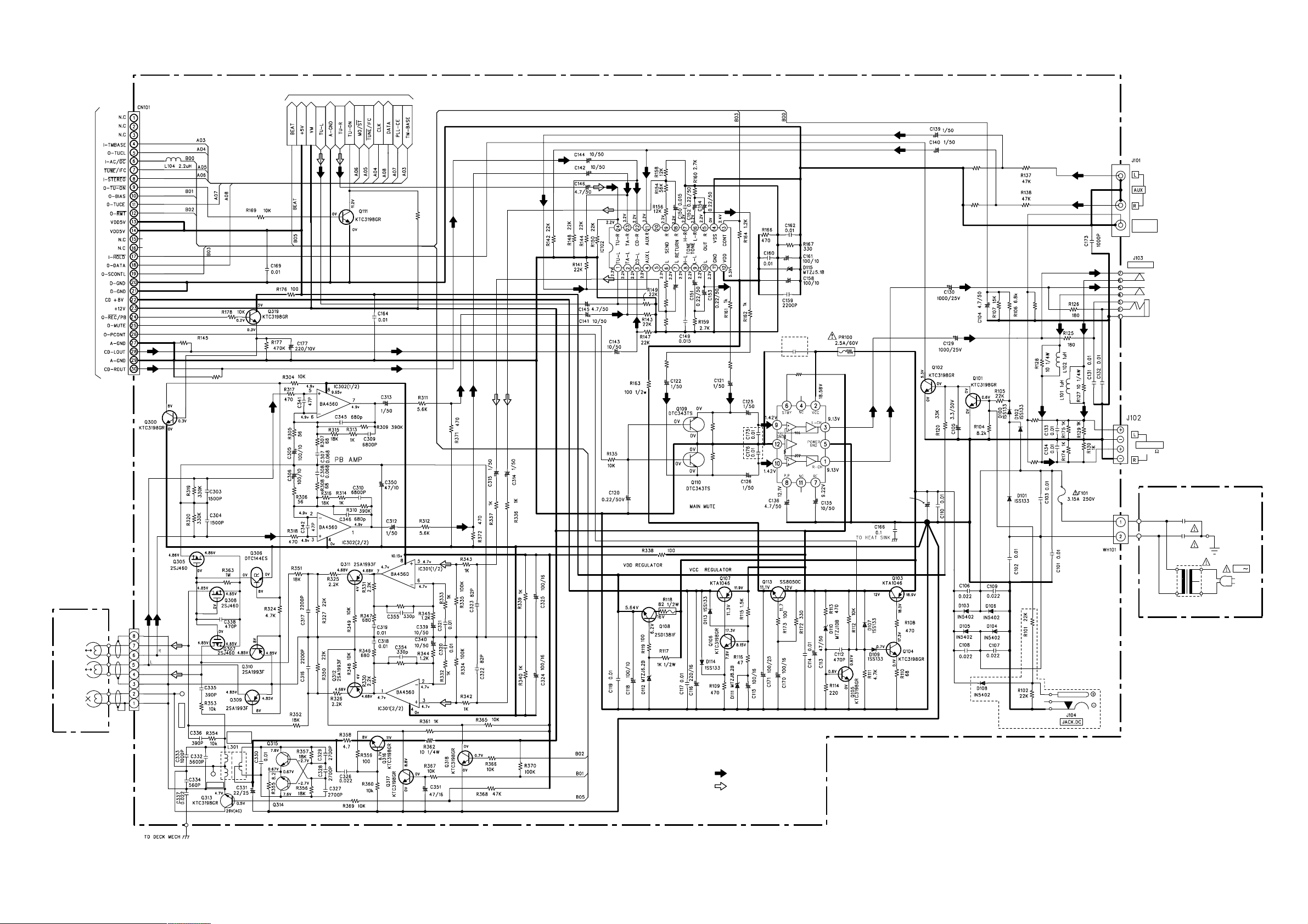
SCHEMATIC DIAGRAM-1/5 (MAIN 1/2)
TO FRONT C.B CN201
MAIN C.B (1/2)
K : 470
HS : 390
R146 K: 470
HS: 390
REC/PB SW
TO MAIN C.B (2/2)
INV.
R168
K : 1.8k
HS : 3.3k
IC102
FUNCTION
SWITCH
M62495AFP
NC NC
R155 12k
C148 47/50
R153 56k
R157
12k
R122
4.7k
C147 47/50
R121
4.7k
K
C174
0.1
1.35V
R134
12K
R139
8.2K
R140
8.2K
Q101,102
HOLD DET
R133
1.2k
SUPER
WOOFER
PHONES
TAPE MECHANIM
(1/2)
(2ZM-1 YR12NC)
RCH
LCH
EX
CN301
INV.
Q305,307,308
REC/PB SW
TP9
REC BIAS
REC BIAS
BEAT CUT
TP8
REC/PB SW
REC/PB SW
REC BIAS
ADJ.
INV.
Q314,315 BIAS OSC
2SC3331T
2SC3331T
IC302
BA4560F
Q311,312
RMT SW
IC301
BA4560F
REC AMP
R329 15k
R328 15k
REG
SW
R123
Q108
Q109,110
Q106,107
1.2k
R124
1.2k
K
IC101
LA4629
POWER AMP
C111
4700/35
Y
Y
REGREG
SW
R131
22k
R132 22k
FC101 FC102
SPEAKER
IMP:4
AC C.B
CNA101
C219
0.01
C220
0.01
PT101
AC
K : 230V 50Hz
HS : 220V 60Hz
K
1/4W
POWER CONT
SIGNAL :
INV.
: PB/FM
: REC/AM
-16-
Page 17
SCHEMATIC DIAGRAM-2/5 (MAIN 2/2 : K MODEL)
MAIN C. B (2/2)
TO MAIN C.B (1/2)
TM-BASE
PLL-CE
(K MODEL)
711
TUNER
ON/OFF
SWITCH
TRACKING
TP2 TP3
DC BAL.
ADJ.
FM/MW IF
SYSTEM
MW IF ADJ.
MS2
AM OSC COIL
MW VT
ADJ.
Q805
IF AMP
BAND
SW
BAND SW
100
MW RF AMP.
6ZA-1 YFEENC
TP1
AM ANT COIL
MW TRACKING
ADJ.
ANTENNA
FM 75
(COAXTAL)
MW/LW
LOOP
A05
TP6FM IF
TP7
MW
IF
TP4, 5
TP4
LW VT ADJ.
2SD1306E
2SD1306E
Q948, 952
BAND SW
SIGNAL :
: PB/FM
: REC/AM
TC942, L941
LW TRACKING
ADJ
-17-
Page 18
SCHEMATIC DIAGRAM-3/5 (MAIN 2/2 : HS MODEL)
TO MAIN C.B (1/2)
MAIN C.B (2/2)
(HS MODEL)
X721
4.500MHz
Q711
TUNER
ON/OFF
SWITCH
TRACKING
TP2 TP3
1500p
1500p
TP6
FM IF
DC BAL.
ADJ.
TP7
AM IF
FM/AM IF
SYSTEM
AM IF ADJ.
10.7MHz
Q805
2SC27140
IF AMP
AM OSC COIL
AM TRACKING
ADJ.
10.7MHz
BAND SW
FFE801
8ZA-1 FEUNC
AM ANT COIL
AM VT
ADJ.
ANTENNA
FM
75
AM
LOOP
3.9k
3.9k
1k
1k
DC
BAL.
DC BAL.
SIGNAL :
: PB/FM
: REC/AM
-18-
Page 19

WIRING-3/3 (FRONT)
101112131415161718192021222324
1234567892526272829303132
FRONT C.B
S219
POWER
C218
C203
R289
R290
R254
K
D204
D207
50
LCD201
110 20 30 4043
R260
R278
D211
IC202
REMOTE
SENSSOR
IC202
R214
30
31
IC201
805181
C210
Q203
EC
B
R267
1
2
3
R233
R268
R280
CN202
R210
3
2
1
D212
R231
C208
X201
R234
1
R230
S206
TAPE
C211
R232
2
TO MAIN C.B CN101
R213
D208
C202
C206
R211
R248
L202
R250
C215
X202
C212
S202
TUNER/BAND
1
100
S204
AUX
S208
CD
L201
D202
CN201
10 20
C205
R251
R247
Q201
R217
B
C
E
R256
D213
C217
R212
C216
Q202
C
E
C214
B
C213
R269
R255
R270
R271
R221
R220
R222
R226
D201
R227
C201
R218
R281
S213
SET
S215
DOWN
S209
DIR/PRESET
S207
S200
CLEAR
R225
R223
HS MODEL K MODEL
MOTOR C.B
MOTOR C.B
A
M2
S205
TIMER/SLEEP
R243
_
+
6
PIN3
1
M2
(SLED MOTOR)
SW1
(INSIDE LIMIT SW)
(SPINDLE MOTOR)
SW1
_
M3
B
M3
+
M3
C
D
M3
30
29
FB201
R228
R209
CD C.B
E
F
S214
JAZZ
R237
S218
ROCK
R235
S216
POP
R242
R241
Q206
R240
D206
Q207
C239
S217
R229
REC
C207
UP
R259
S201
VOL+
R238
R272
R258
Q204
Q205
B
C
C204
R205
CEB
CEB
R207
CEB
R202
E
R206
R201
R204
S203
VOL–
R236
R208
R203
R482
R481
CNA203
D520
D494
D491
C458
C457
CN403
R467
1
2
C459
Q491
C482
C481
L404
BC E
C462
C489
C491
D402
R501
C501
R491
X401
R502
R492
C490
R455
C502
R465
R503
C496
C465
C503
C494
48
49
R466
R505
BC E
C505
C461
R506
Q492
C463
C460
C506
C464
R504
CN402
C492
C467
C504
1
6
33
C478
C466
32
IC402
164
R480
R490
1
9
C476
C475
C471
C477
R441
C470
C445
R444
R442
C446
R443
C455
C472
R469
17
16
30
16
R475
L403
C447
C451
IC403
R477
R438
R507
R440
ECB
C441
R439
C442
C448
1
C473
R445
15
Q402
C469
R437
R446
C474
R436
R435
D403
C479
R434
R476
R432
R431
C439
C432
R428
C438
R452
C480
R451
C434
R424
R425
R423
C450
C433
R427
R429
C431
C430
32
33
R499
R489
2
116
R530
SFR430
R531
R532
C429
R421
R419
R420
R457
C425
C428
R410
R448
R447
16
17
IC401
C437
49
48
R433
C414
CN401
R413
R411
C510
R418
R417
C426
R414
C435
R430
R426
R415
C424
C413
C436
C423
C422
R412
R403
R416
C421
1
64
C412
15
B
E
C411
Q406
B
C415
C406
Q403
E
C418
C405
Q408
C
B
E
C417
C420
C404
R402
R486
C
B
E
C403
R479
R496
C
Q407
R488
C416
R405
C419
R408
R409
C402
R401
BCE
R485
C
R478
R406
FFC401
R487
R495
R497
R498
R456
R453
C407
C408
C410
D401
C409
Q401
TO OPTICAL PICK UP
(SF-P101NR): HS MODEL
(KSS-213C): K MODEL
C401L401
G
H
I
J
K
L
M
N
O
P
LED C.B
D941
D942
D943
D944
D945
D941-949
(LCD BACK LIGHT)
D946
D947
(CD DOOR SW)
R264R261R265R262R266R263
D948
D949
CN204
123
DECK C.B
CrO2
Q
R
S
T
U
CRD1
-19-
Page 20

SCHEMATIC DIAGRAM-4/5 (FRONT)
FRONT C. B
REG.
TO MAIN C.B (1/2) CN101
IC201
LC867248A-5V96
SYSTEM CONTROL
LCD201
ZCL-8
LED C. B
CN204
D941-949
SLR-342 MGT32
(LCD BACK LIGHT)
D-SW
K
NC
NC
NC
33k
18k
TO CD C.B
10k
9.1k
BEAT SW
SIGNAL :
FB201
TO CD C.B
: PB/FM
Q204-207
REC/PLAY SW
CD
AUX
CLEAR
RESET
REC
DOWN
SET
DIR/PRESET
UP
VOL–
VOL+
-20-
Page 21

SCHEMATIC DIAGRAM-5/5 (CD : HS MODEL)
CD MECHANISM
(DA11T3C):161HS
OPTICAL
PICK UP
(SF-P101NR):161HS
CN1
CD C.B
SW
INV.
CN401
(HS MODEL)
LD DRIVE
SW
SW
N.C.
MOTOR C.B
PIN3
M3
M2
SW1
FFC401
5V
SERVO DRIVE
REG
SIGNAL
: PB
CNA203
CAM
SOL
AUT
GND
CST
B+ MOT
REC A
REC B
Q491,492
8V REG.
TO FRONT C.B
TAPE MECHANISM (2/2)
(2ZM-1 YR12NC)
IC1
DN6851
TO FRONT C.B
CRD1
-21-
DECK C.B
Page 22

SCHEMATIC DIAGRAM-5/5 (CD : K MODEL)
CD MECHANISM
(KSM213CDM):161K
OPTICAL
PICK UP
(KSS-213C):161K
CN1
CD C.B
SW
INV.
CN401
(K MODEL)
LD DRIVE
SW
SW
N.C.
MOTOR C.B
PIN3
M3
M2
SW1
FFC401
5V
SERVO DRIVE
REG
SIGNAL
: PB
CNA203
CAM
SOL
AUT
GND
CST
B+ MOT
REC A
REC B
Q491,492
8V REG.
TO FRONT C.B
TAPE MECHANISM (2/2)
(2ZM-1 YR12NC)
IC1
DN6851
TO FRONT C.B
CRD1
-21 a-
DECK C.B
Page 23

FL (ZCL-8) GRID ASSIGNMENT/ANODE CONNECTION-1/1
GRID ASSIGNMENT
ANODE CONNECTION
-22-
Page 24

ELECTRICAL ADJUSTMENT-1/13 (K MODEL)
BAL.ADJ.
TP2:Rch OUT
TP3:Lch OUT
TP7:MW IF
TP4,5:DC BAL.
REC BIAS ADJ. POINT
TP9:REC BAIS TEST POINT
AUX
O
HEAD PHONE
-23-
Page 25

ELECTRICAL ADJUSTMENT-2/13 (K MODEL)
Hz
WOW&FLU TTER M ETER
HP OUT
%
INPUT
Hz
WOW&FLU TTER M ETER
HP OUT
%
INPUT
DECK ADJUSTMENT
DECK C.B.
TAPE SPEED ADJ.
HEAD AZIMUTH ADJ.
1. TAPE SPEED ADJUSTMENT
Requirements
• Measuring equipments : wow-flutter meter (frequency counter )
Test Tape : TTA-100 (3KHz)
Test point : HP OUT
Adjustment point : SFR1
1)Connect HP OUT to the Wow - flutter meter.
2)Insert the test tape (TTA-100), play back center of the tape and adjust SFR1 until it becomes
3,000Hz±5Hz.
3) RVS playback and check that ±45Hz is added according to the FWD speed.
2. WOW - FLUTTER CHECK
Requirements
Test tape : TTA-100 (3KHz)
Test point : HP OUT
1)Connect the HP OUT to the Wow - flutter meter.
2)Set the indicator to JIS and the mode to W RMS (WTD) of the Wow - flitter meter.
3)Play back thee center of the test tape (TTA-100) and check that it is below 0.35%.
3. HEAD AZIMUTH ADJUSTMENT
Requirements
• Measuring equipment : Oscilloscope
Test Tape : TTA-330 (8KHz)
Test point : HP OUT
Adjustment point : Head azimuth screw
1)Connect the HP OUT to the oscilloscope of CH1 and CH2.
2)Set the V mode of the oscilloscope to ADD.
3)Insert the test tape (TTA-330) , play back the center of the tape and adjustment the head azimuth
screw until the waveform of the oscilloscope has reached the maximum when playing back at 10KHz.
4) Reverse the tape, RVS playback and adjust, using the head azimuth screws until the waveform of the
oscilloscope has reached its maximum.
5) After the adjustment, bond lock (1600B) the screw.
OSCILLOSCOPE
OUTPUT
CH1 CH2
Lch
Rch
-24-
Page 26

ELECTRICAL ADJUSTMENT-3/13 (K MODEL)
4. REC. BIAS FREQUENCY ADJUSTMENT
Requirement
• Measuring equipment: frequency counter
Test point : TP9
Adjustment point : L301
1)Connect the TP9 to the frequency counter.
2)Set the recording condition to the main unit.
3)Adjust the L301 until it becomes 85KHz±5KHz.
FREQUENCY COUNTER
Hz
TP9
GND
-25-
Page 27

ELECTRICAL ADJUSTMENT-4/13 (K MODEL)
V
DIGITAL MULTIMETER
TP1
GND
TUNER ADJUSTMENT
1. VT ADJUSTMENT (LW)
Requirement
• Measuring equipment : Digital multi-meter
Test point : TP1(FFE801 4pin),GND
Adjustment point : L942
(1) Adjust the reception frequency of the main unit to 290KHz.
(2) Adjust L942 until the test point voltage (VT) is 5.5V±0.1V.
(3) Adjust the reception frequency of the main unit to 144KHz.
(4) Check that the test point (VT) voltage is below 2.5V.
2. VT ADJUSTMENT (MW)
Requirement
• Measuring equipment : Digital multi-meter
Test point : TP1(FFE801 4pin),GND
Adjustment point : L774
DIGITAL MULTIMETER
V
(1) Adjust the reception frequency of the main unit to 1602KHz.
(2) Adjust L773 until the test point voltage (VT) is 5.5V±0.1V.
(3) Adjust the reception frequency of the main unit to 531KHz.
(4) Check that the test point (VT) voltage is below 2.0V.
3. VT CHECK (FM)
Requirement
• Measuring equipment : Digital multi-meter
Test point : TP1(FFE801 4pin),GND
(1) Adjust the reception frequency of the main unit to 108.0MHz.
(2) Check that the test point (VT) voltage is about 8.0V.
(3) Adjust the reception frequency of the main unit to 87.5MHz.
(4) Check that the test point (VT) voltage is about 2.5V.
4. DC BALANCE ADJUSTMENT
Requirement
• Measuring equipment : Digital multi-meter
Test point : TP4, 5
Adjustment point : L771
(1) Adjust the reception frequency of the main unit to 98.0MHz.
(2) Adjust L771 until the test point voltage difference between TP4 and TP5 is 0mV±20mV.
TP1
GND
DIGITAL MULTIMETER
V
VT
GND
DIGITAL MULTIMETER
V
VT
GND
-26-
Page 28

ELECTRICAL ADJUSTMENT-5/13 (K MODEL)
e
R
R
<MW / LW ADJUSTMENT>
For MW / LW adjustment, do wiring and connection as in the following.
60cm
Standerd Signal Generaor
Fig. 2
5. IF ADJUSTMENT (MW)
Requirement
• Measuring equipment : Oscilloscope or Millivoltmeter
Test point : TP7 (IC771 24pin), GND
Adjustment point : L772
(1) Adjust the setting of Standard Signal Generator (hereinafter S.S.G.) to 450KHz of 30%
variation.
(2) While looking at the waveform on the oscilloscope, reduce the output level all the way.
(3) Adjust L772 until the waveform of the oscilloscope reaches the maximum.
6. TRACKING ADJUSTMENT (MW)
Requirement
• Measuring equipment : Millivoltmeter
Test point : TP2, TP3, GND
Adjustment point : L773
(1) Adjust the S.S.G. setting to 1000KHz of 30% variation and reduce the output level all the way.
(2) Adjust the reception frequency of the main unit to 1000KHz.
(3) Adjust L773 until the value of the millivoltmeter reaches the maximum.
SET
Lch
Rch
GND
TP
CH1 CH2
Lch
Rch
GND
AC MILLI VOLTMETE
TP2
GND
TP3
Connect t o the respectiv
measuring equipment
OSCILL OSCOPE
GND
CH2
CH1
GND
7. TRACKING ADJUSTMENT (LW)
Requirement
• Measuring equipment : Millivoltmeter
Test point : TP2, TP3, GND
Adjustment point : TC941, L941
(1) Adjust the S.S.G. setting to 290KHz of 30% variation and reduce the output level all the way.
(2) Adjust the reception frequency of the main unit to 290KHz.
(3) Adjust LTC941 until the value of the millivoltmeter reaches the maximum.
(4) Adjust the S.S.G. setting to 144KHz of 30% variation and reduce the output level all the way
(5) Adjust the reception frequency of the main unit to 144KHz
(6) Adjust LTC941 until the value of the millivoltmeter reaches the maximum.
(7) Repeat the adjustment 2 to 3 times from 1 to 6 above.
-27-
AC MILLI VOLTMETE
TP2
GND
TP3
CH1
CH2
GND
Page 29

ELECTRICAL ADJUSTMENT-6/13 (K MODEL)
R
<FM ADJUSTMENT>
For adjusting FM, do wiring function and connection as in the following.
Standerd Signal Generaor
SET
Lch
Rch
GND
TP
Connect to the respective
measuri ng equi pment
Fig. 1
8. TRACKING CHECK
Requirement
• Measuring equipment : millivoltmeter
Test point : TP2, TP3, GND
(1) Adjust the S.S.G. setting to 83.0MHz of 75KHz variation, and 66dBuV for the output level.
(2) Check that the test point voltage is about 400mV.
AC MILLI VOLTMETE
TP2
GND
TP3
CH1
CH2
GND
-28-
Page 30

ELECTRICAL ADJUSTMENT-7/13 (HS MODEL)
BAL.ADJ.
TP2:Rch OUT
TP3:Lch OUT
TP4,5:DC BAL.
TP7:AM IF
REC BIAS ADJ. POINT
TP9:REC BAIS TEST POINT
AUX
O
HEAD PHONE
-29-
Page 31

ELECTRICAL ADJUSTMENT-8/13 (HS MODEL)
Hz
WOW&FLU TTER M ETER
HP OUT
%
INPUT
Hz
WOW&FLU TTER M ETER
HP OUT
%
INPUT
DECK ADJUSTMENT
DECK C.B.
TAPE SPEED ADJ.
1. TAPE SPEED ADJUSTMENT
Requirements
• Measuring equipments : wow-flutter meter (frequency counter )
Test Tape : TTA-100 (3KHz)
Test point : HP OUT
Adjustment point : SFR1
HEAD AZIMUTH ADJ.
1)Connect HP OUT to the Wow - flutter meter.
2)Insert the test tape (TTA-100), play back center of the tape and adjust SFR1 until it becomes
3,000Hz±5Hz.
3)RVS playback and check that ±45Hz is added according to the FWD speed.
2. WOW - FLUTTER CHECK
Requirements
Test tape : TTA-100 (3KHz)
Test point : HP OUT
1)Connect the HP OUT to the Wow - flutter meter.
2)Set the indicator to JIS and the mode to W RMS (WTD) of the Wow - flitter meter.
3)Play back thee center of the test tape (TTA-100) and check that it is below 0.35%.
3. HEAD AZIMUTH ADJUSTMENT
Requirements
• Measuring equipment : Oscilloscope
Test Tape : TTA-330 (8KHz)
Test point : HP OUT
Adjustment point : Head azimuth screw
1)Connect the HP OUT to the oscilloscope of CH1 and CH2.
2)Set the V mode of the oscilloscope to ADD.
3)Insert the test tape (TTA-330) , play back the center of the tape and adjustment the head azimuth
screw until the waveform of the oscilloscope has reached the maximum when playing back at
10KHz.
4)Reverse the tape, RVS playback and adjust, using the head azimuth screws until the waveform of the
oscilloscope has reached its maximum.
5)After the adjustment, bond lock (1600B) the screw.
OSCILLOSCOPE
OUTPUT
CH1 CH2
Lch
Rch
-30-
Page 32

ELECTRICAL ADJUSTMENT-9/13 (HS MODEL)
4. REC. BIAS FREQUENCY ADJUSTMENT
Requirement
• Measuring equipment : frequency counter
Test point : TP9
Adjustment point : L301
1)Connect the TP9 to the frequency counter.
2)Set the recording condition to the main unit.
3)Adjust the L301 until it becomes 85KHz±5KHz.
FREQUENCY COUNTER
Hz
TP9
GND
-31-
Page 33

ELECTRICAL ADJUSTMENT-10/13 (HS MODEL)
e
V
DIGITAL MULTIMETER
TP1
GND
V
DIGITAL MULTIMETER
TP1
GND
GND
OSCILL OSCOPE
CH1 CH2
Lch
Rch
GND
TUNER ADJUSTMENT
1. VT ADJUSTMENT (AM)
Requirement
• Measuring equipment : Digital multi-meter
Test point : TP1(FFE801 4pin),GND
Adjustment point : L773
(1) Adjust the reception frequency of the main unit to 1602KHz.
(2) Adjust L773 until the test point voltage (VT) is 8.5V±0.5V.
(3) Adjust the reception frequency of the main unit to 531KHz.
(4) Check that the test point (VT) voltage is about 1.3V.
2. VT CHECK (FM)
Requirement
• Measuring equipment : Digital multi-meter
Test point : TP1(FFE801 4pin), GND
(1) Adjust the reception frequency of the main unit to 108.0MHz.
(2) Check that the test point (VT) voltage is about 8.0V.
(3) Adjust the reception frequency of the main unit to 87.5MHz.
(4) Check that the test point (VT) voltage is about 2.5V.
3. DC BALANCE ADJUSTMENT
Requirement
• Measuring equipment : Digital multi-meter
Test point : TP4, 5
Adjustment point : L771
(1) Adjust the reception frequency of the main unit to 98.0MHz.
(2) Adjust L771 until the test point voltage difference between TP4 and TP5 is 0mV±20mV.
<ADJUSTMENT>
For AM adjustment, do wiring and connection as in the following.
60cm
Standerd Signal Generaor
Fig.2
SET
Lch
Rch
GND
VT
GND
TP
DIGITAL MULTIMETER
V
Connect t o the respectiv
measuring equipment
4. IF ADJUSTMENT
Requirement
• Measuring equipment : Oscilloscope or Millivoltmeter
Test point : TP7 (IC771 24pin), GND
Adjustment point : L772
(1) Adjust the setting of Standard Signal Generator (hereinafter S.S.G.) to 450KHz of 30% variation.
(2) While looking at the waveform on the oscilloscope, reduce the output level all the way.
(3) Adjust L802 until the waveform of the oscilloscope reaches the maximum.
-32-
Page 34

ELECTRICAL ADJUSTMENT-11/13 (HS MODEL)
R
R
5. TRACKING ADJUSTMENT
Requirement
• Measuring equipment : Millivoltmeter
Test point : TP2, TP3, GND
Adjustment point : L774
(1) Adjust the S.S.G. setting to 999KHz of 30% variation and reduce the output level all the way.
(2) Adjust the reception frequency of the main unit to 999KHz.
(3) Adjust L774 until the value of the millivoltmeter reaches the maximum.
<FM ADJUSTMENT>
For adjusting FM, do wiring function and connection as in the following.
Standerd Signal Generaor
SET
TP
Lch
Rch
GND
Fig.1
6. TRACKING CHECK
Requirement
• Measuring equipment : millivoltmeter
Test point : TP2, TP3, GND
(1) Adjust the S.S.G. setting to 98.0MHz of 75KHz variation, and 66dBuV for the output level.
(2) Check that the test point voltage is about 400mV.
AC MILLI VOLTMETE
TP2
GND
TP3
Connect to the respective
measuri ng equi pment
AC MILLI VOLTMETE
TP2
GND
TP3
CH1
CH1
CH2
GND
CH2
GND
-33-
Page 35

ELECTRICAL ADJUSTMENT-12/13
V
DIGITAL MULTIMETER
FE
Vref
OUTPUT
OSCIL LOSCOPE
RF SW
Vref
VOLT/ DIV: 500mV
TIME / DIV: 0.2 s
EYE PATTERN
must be CLEAR and MAX
Approx.
1.8 0.3Vp.p
CD ADJUSTMENT
CD PWB
PATTERN SI DE PARTS SI DE
R401
R402
RF S W
Vref
IC401
FE
IC402
• Perform the adjustments after the main unit enters the test mode.
• Place the CD mechanism on level ground.
• Equipment and tools required
Measuring equipment
Digital multi-meter
Jitter meter (KIKUSUI 6235)
Test disc : TCD-782
ATD-001
SFR430
IC403
1
5
2
3
1
1 2 3
1.FOCUS BAIS ADJUSTMENT
1)Connect the digital multi-meter to the test point FE and Vref.
2)Play back the 2nd track of TCD-782.
3)Adjust SFR430 until the digital multi-meter indicates 0±10mV.
2.RF WAVEFORM CHECK
1)Connect oscilloscope to the test point RF SW and Vref.
2) Play back the 2nd track of TCD-782.
3)Check that the RF waveform has the maxmum amplitude and the center of the wedge waveform has
the clear blank.
-34-
Page 36

ELECTRICAL ADJUSTMENT-13/13
OUTPUT
ns
OSCILLOSCOPE
JITTER METER
INPUT
RF SW
Vref
V
DIGITAL MULTIMETER
R402
R402
3. JITTER CHECK
1)While oscilloscope is kept connected in the same test point as in step2. RF
WAVEFORM CHECK, connect the output terminal of an oscilloscope to the
input terminal of the jitter meter.
2)Set the VOLT range selector of oscilloscope to 500mV range or below.
3)Play back 2nd track of TCD-782.
4)Check that jitter meter indicates 28.0ns or less.
4. PLAY ABILITY CHECK
1)Play back the 3rd , 8th and 13th track of ATD-001. Check that the noise does not
occur sound skipping does not occur.
5. LASER CURRENT CHECK
* Do not perform this measurement unless the laser is suspected to be defective.
1)Connect digital multi-meter across the resistor R402(10Ω).
2)Play back the TCD-782 and check the DC voltage value on the digital multi-
meter.
3)Calculate the laser current (Iop) by dividing the DC voltage across R402 by the
resistor value (R402= 10Ω). Check that the laser current (Iop) is 60mA or less.
-35-
Page 37

CD TEST MODE-1/1
1. How to Start the CD Test Mode
While pressing the CD FUNCTION button, insert the AC plug to the power outlet.
When the test mode started, all lights on the display are lit.
2. How to Exit the CD Test Mode
Press the POWER button or press the other FUNCTION buttons or disconnect the AC plug.
3. Function and Usage of the CD Test Mode
No
1
2
3
4
*1: The driver IC heats up and the protection circuit starts working when the focus search is continued for 10 minutes or longer.
There can be a case that operations cannot be performed correctly. In such a case, turn off the main power. After cooling down
the machine, restart the machine.
Mode
Start Mode
Search Mode
(without disc)
Play Mode
Sled Mode
Button for
Activation
PLAY button
PLAY button
FF button
RWD button
Display
All lights are lit.
Normal
Normal
Operation
• LD illuminates all the time
• Focus search continues
operations *1
• Spindle motor continuous kick
• Normal playback
• If TOC cannot be read, focus
search is continued
• Pickup moves to the inner
circumference *2
• Pickup is moves to the outer
circumference *2
Contents
• FL check
• Microcomputer check
• APC circuit check
• Laser current measurement
• Focus search waveform check
• Focus error waveform check
(DRF in the search mode is
ignored)
• Each servo circuit is checked
• DRF check
• Sled circuit check
• Mechanism operation check
• Pickup check
*2: Be careful not to damage the gear because the sled motor rotates while the FF or RWD button is being pressed even if the
pickup is located in the innermost track or the outermost track.
-36-
Page 38

IC BLOCK DIAGRAM-1/2
IC, LA1837NL
AM LBO/
FM SD ADJ
FM IN
REG
AM LO
FM IF REF
AM IF OUT
AM RF
AM IF IN
S CURVE
GND
AGC
TUNE
AM DET OUT
FM DET OUT
VCC
ST/
AM IFO
DET IN
FM DET
L OUT
R OUT
FM VSM
AM SD BW
L IN
SD ADJ
AM VSM/
R IN
IF BO
FM/AM
MONO
IC, LA6541D
-37-
Page 39

IC BLOCK DIAGRAM-2/2
IC, M62495AFP
IC, LC72131D
AUTO RESET
-38-
Page 40

IC DESCRIPTION-1/3 (LA9241ML)-1/2
Pin No. Pin Name I/O Description
1
2
FIN2
FIN1
Pin to which external pickup photo diode is connected. RF signal is created by adding with the
I
FIN1 pin signal. FE signal is created by subtracting from the FIN1 pin signal.
I
Pin to which external pickup photo diode is connected.
10
11
12
13
14
15
16
17
3
4
5
6
7
8
9
E
F
TB
TE–
TE
TESI
SCI
TH
TA
TD–
TD
JP
TO
FD
FD–
Pin to which external pickup photo diode is connected. TE signal is created by subtracting from
I
the F pin signal.
I
Pin to which external pickup photo diode is connected.
I
DC component of the TE signal is input.
I
Pin to which external resistor setting the TE signal gain is connected between the TE pin.
O
TE signal output pin.
TES “Track Error Sense” comparator input pin. TE signal is passed through a band-pass filter
I
then input.
I
Shock detection signal input pin.
I
Tracking gain time constant setting pin.
O
TA amplifier output pin.
Pin to which external tracking phase compensation constants are connected between the TD and
I
VR pins.
I
Tracking phase compensation setting pin.
I
Tracking jump signal (kick pulse) amplitude setting pin.
O
Tracking control signal output pin.
O
Focusing control signal output pin.
Pin to which external focusing phase compensation constants are connected between the FD and
I
FA pins.
18
19
20
21
22
23
24
25
26
27
28
29
30, 31
32, 33
34
FA
FA–
FE
FE–
AGND
SP
SP–
SPG
SP–
SPD
SLEQ
SLD
SL–, SL+
JP–, JP+
TGL
—
—
Pin to which external focusing phase compensation constants are connected between the FD–
I
and FA– pins.
Pin to which external focusing phase compensation constants are connected between the FA and
I
FE pins.
O
FE signal output pin.
I
Pin to which external FE signal gain setting resistor is connected between the FE pin.
Analog signal GND.
Single ended output of the CV+ and CV– pin input signal.
O
Spindle amp input.
I
Pin to which external spindle gain setting resistor in 12 cm mode is connected.
Pin to which external spindle phase compensation constants are connected together with SPD
I
pin.
O
Spindle control signal output pin.
I
Pin to which external sled phase compensation constants are connected.
O
Sled control signal output pin.
I
Sled advance signal input pin from microprocessor.
I
Tracking jump signal input pin from DSP.
I
Tracking gain control signal input from DSP. Low gain when TGL = H.
35
TOFF
I
Tracking off control signal input pin from DSP. Off when TOFF = H.
-39-
Page 41

IC DESCRIPTION-1/3 (LA9241ML)-2/2
Pin No. Pin Name I/O Description
36
TES
O
Pin from which TES signal is output to DSP.
37
38
39, 40
41
42
43
44
45
46
47
48
49
50
51
52
53
54
HFL
SLOF
CV–, CV+
RFSM
RFS–
SLC
SLI
DGND
FSC
TBC
NC
DEF
CLK
CL
DATA
CE
DRF
—
—
“High Frequency Level” is used to judge whether the main beam position is on top of bit or on
O
top of mirror.
I
Sled servo off control input pin.
I
CLV error signal input pin from DSP.
O
RF output pin.
I
RF gain setting and EFM signal 3T compensation constant setting pin together with RFSM pin.
O
“Slice Level Control” is the output pin which controls the RF signal data slice level by DSP.
I
Input pin which control the data slice level by the DSP.
Digital system GND.
O
Output pin to which external focus search smoothing capacitor is connected.
I
“Tracking Balance Control” EF balance variable range setting pin.
No connection.
O
Disc defect detector output pin.
I
Reference clock input pin. 4.23 MHz of the DSP is input.
I
Microprocessor command clock input pin.
I
Microprocessor command data input pin.
I
Microprocessor command chip enable input pin.
O
“Detect RF” RF level detector output.
55
56
57
58
59
60
61
62
63
64
FSS
VCC2
REFI
VR
LF2
PH1
BH1
LDD
LDS
VCC1
—
—
—
I
“Focus Search Select” focus search mode (± search/+ search) select pin.
Servo system and digital system Vcc pin.
Pin to which external bypass capacitor for reference voltage is connected.
O
Reference voltage output pin.
I
Disc defect detector time constant setting pin.
I
Pin to which external capacitor for RF signal peak holding is connected.
I
Pin to which external capacitor for RF signal bottom holding is connected.
O
APC circuit output pin.
I
APC circuit input pin.
RF system Vcc pin.
-40-
Page 42

IC DESCRIPTION-2/3 (LC78622NE)-1/2
Pin No. Pin Name I/O Description
1
2
3
DEFI
TAI
PDO
I
Defect sense signal (DEF) input pin. (Connect to 0V when not used)
I
O
Test signal input pin with built-in pull-down resistor. Be sure to connect to 0V.
Phase comparator output pin to control external VCO.
4
5
6
7
8
9
10
11
12, 13
14
15
16
17
18
19, 20
21
VVSS
ISET
VVDD
FR
VSS
EFMO
EFMIN
TEST2
CLV+, CLV–
___
V/P
HFL
TES
TOFF
TGL
JP+, JP–
PCK
—
—
—
For PLL.
I
GND pin for built-in VCO. Be sure to connect to 0V.
Pin to which external resistor adjusting the PD0 output current.
Power supply pin for built-in VCO.
I
Pin for VCO frequency range adjustment.
Digital system GND. Be sure to connect to 0V.
O
For slice level control.
I
I
Test signal input pin with built-in pull-down resistor. Be sure to connect to 0V.
O
Disc motor control output. Three level output is possible using command.
EFM signal output pin.
EFM signal input pin.
Rough servo or phase control automatic selection monitoring output pin. Rough servo at H.
O
Phase servo at L.
I
Track detect signal input pin. Schmidt input.
I
Tracking error signal input pin. Schmidt input.
O
Tracking OFF output pin.
O
Tracking gain selection output pin. Gain boost at L.
O
Track jump control signal output pin. Three level output is possible using command.
O
EFM data playback clock monitoring pin 4.3218 MHz when phase is locked in.
22
23
24
25
26
27
28
29
30
31
32, 33
34
35
36
37
38
39
40
41
FSEQ
VDD
SL+
SL-
CONT3
PUIN
_______
RW
EMPH
C2F
DOUT
TEST3, TEST4
NC
MUTEL
LVDD
LCHO
LVSS
RVSS
RCHO
RVDD
O
—
I/O
I/O
I/O
I/O
I/O
O
O
O
I
—
O
—
O
—
—
O
—
Sync signal detection output pin. H when the sync signal which is detected from EFM signal and
thesync signal which is internally generated agree. (Not connected)
Digital system power supply pin.
The pin is controlled by the serial data
command from microprocessor. When
the pin is not used, set the pin to the input
General purpose input/output pin 1 to 5.
terminal and connect to 0V, or alternately
set the pin to output terminal and leave
the pin open.
De-emphasis monitor output pin. De-emphasis disc is being played back at H. (Not connected)
C2 flag output pin. (Not connected)
DIGITAL OUT output pin. (EIAJ format)
Test signal input pin with built-in pull-down resistor. Be sure to connect to 0V.
Not used. Set the pin to open.
L-channel mute output pin. (Not connected)
L-channel 1-bit DAC.
L-channel power supply pin.
L-channel output pin.
L-channel GND. Be sure to connect to 0V.
R-channel GND. Be sure to connect to 0V.
R-channel 1-bit DAC.
R-channel output pin.
R-channel power supply pin.
42
MUTER
O
R-channel mute output pin. (Not connected)
-41-
Page 43

IC DESCRIPTION-2/3 (LC78622NE)-2/2
Pin No. Pin Name I/O Description
43
44
45
XVDD
XOUT
XIN
—
Crystal oscillator power supply pin.
O
Pin to which external 16.9344 MHz crystal oscillator is connected.
I
46
47
48
49
50
51
52
53
54
55
56
57
58
59
60
61
62
63
XVSS
SBSY
EFLG
PW
SFSY
SBCK
FSX
WRQ
RWC
SQOUT
COIN
___________
CQCK
________
RES
TST11
16M
4.2M
TEST5
______
CS
—
Crystal oscillator GND pin. Be sure to connect to 0V.
O
Subcode block sync signal output pin. (Not connected)
O
C1, C2, single and dual correction monitoring pin. (Not connected)
O
Subcode P, Q, R, S, T, U and W output pin. (Not connected)
Subcode frame sync signal output pin. Falls down when subcode enters standby. (Not
O
connected)
I
Subcode read clock input pin. Schmidt input. (Be sure to connected to 0V when not in use)
Pin outputting the 7.35 kHz sync signal which is generated by dividing frequency of crystal
O
oscillator. (Not connected)
O
Subcode Q output standby output pin.
I
Read/write control input pin. Schmidt input.
O
Subcode Q output pin.
I
Command input pin from microprocessor.
I
Command input read clock or subcode read input clock from SQOUT pin
I
LC78622 reset input pin. Set this pin to L once when the main power is turned on.
O
Test signal output pin. Use this pin as open (normally L output). (Not connected)
O
16.9344 MHz output pin. (Not connected)
O
4.2336 MHz output pin.
I
Test signal input pin with built-in pull-down resistor. Be sure to connect to 0V.
Chip select signal input pin with built-in pull-down resistor. Be sure to connect to 0V while it is
I
not controlling.
64
TEST1
Test signal input pin without built-in pull-down resistor. Be sure to connect to 0V.
I
Note: The same potential must be applied to the respective power supply terminals. (VDD, VVDD, LVDD, RVDD, XVDD)
-42-
Page 44

IC DESCRIPTION-3/3 (LC867248A-5V96)-1/2
Pin No. Pin Name I/O Description
1
2
3
O-SCONTM
O-SCONTL
O-TUDI
O
M62495AFP control. Open drain output.
O
O
Tuner data output. CMOS output.
4
5
6
7
8
9
10
11
12
13, 14
15
16, 17
18
19
20
21
22
23
24
I-TUDO
O-TUCL
O-COIN
I-SQOUT
___________
O-CQCK
O-RWC
_______________
O-CLKSFT
I-TMBASE
____________
I-RESET
XT1,XT2
VSS1
CF1, CF2
VDD1
I-KEY0
I-KEY1
I-RDSIG
I-WRQ
I-DRF
I-DOOR
I
O
O
I
O
O
O
I
I
I/O
—
I/O
—
I
I
I
I
I
I
Tuner data input. Open drain input.
Tuner clock output. CMOS output.
CD control. CMOS output.
CD control. Open drain input.
CD control. CMOS output.
Clock shift output. “L” during shift. open drain output.
8 Hz time base input.
Reset input. “L” during reset.
32.768kHz crystal.
GND.
Main clock 5.76 MHz.
+5V.
KEY0 A/D input.
KEY1 A/D input.
RDS signal level input. (A/D input)
CD control input.
CD door SW detection SW input. “L” during CLOSE.
25
26
27
28
29
30
31
32
33
34
35
36-38
39-55
56
57
58-79
80
81
82
NC
I-SWTAPE
________________
I-STEREO
I-RDCL
________
I-RMT
___________
I-HOLD
I-RDDT
NC
NC
O-MOTOR
O-PL
NC
S9-S25
VDD2
VSS2
S26-S47
I-CLKDSP
I-AS
__________
I-STOP
—
—
—
I
Not used.
I
Tape detection SW input. (A/D input)
I
Monaural/stereo indication selector input. “L” during stereo.
I
RDS clock input.
I
Remote control input. (fall-down edge interrupt input)
I
Hold mode detection. “L” during hold mode.
I
RDS data input.
I
Not used.
I
Not used.
O
Mechanism deck motor ON/OFF output. “H” during ON. CMOS output.
O
Mechanism deck plunger solenoid ON/OFF output. “H” during ON. CMOS output .
O
Not used.
O
LCD SEG terminal Initial setting output. (S10 to S17)
+5V.
GND.
LCD SEG terminal .
I
Watch indication select input “L”: 12H. “H”: 24H.
I
Auto stop. counter input .
Tape stop input. “L” during STOP.
I
-43-
Page 45

IC DESCRIPTION-3/3 (LC867248A-5V96)-2/2
Pin No. Pin Name I/O Description
83-86
87
88
89
90
91
92
COM0-COM3
I-INIT
______
I-AC/DC
VSS3
VDD3
NC
O-TUCE
—
—
—
O
LCD common output.
I
Initial setting input.
I
AC/DC detection.“H” during AC. COMS input.
GND.
5V.
Not used.
O
Tuner chip enable output. CMOS output .
93
94
95
96
97
98
99
100
O-CD-ON
O-TU-ON
O-RMT
_____
O-REC/PB
O-MUTE
O-PCONT
O-BIAS
NC
O
“H” output during CD function. CMOS output.
O
“H” output during TU function. CMOS output.
O
REC mute output. “H” during mute. CMOS output.
O
REC/PB select output. “L” during PB. COMS output.
O
Mute output. “H” during mute. COMS output.
O
Power control output. “H” during ON. CMOS output.
O
REC bias ON/OFF output. “H” at ON. Open drain output.
O
Not used.
-44-
Page 46

MECHANICAL EXPLODED VIEW-1/1
17
14
13
15
16
12
11
HS
20
24
39
43
42
33
22
18
26
FL
19
K
29
KSM213
CDM
43
G
E
26
PWB
27
30
D
43
44
B
A
G
E
PWB
F
HT-SINK
28
A
B
PLATE,SHIELD PT
43
40
25
37
G
E
D
36
38
C
2ZM-1YR12NC
C
35
34
1
32
31
PWB
21
C
B
40
CHAS, MAIN
41
PWB
9
3
H
8
6
5
7
2
23
10
4
G
E
-45-
Page 47

MECHANICAL PARTS LIST-1/1
REF. NO PART NO. KANRI DESCRIPTION
1 88-CL5-202-010 HLDR,CASS LOCKE R
2 8Z-CL8-209-010 SPR-T,CASS
3 8B-CLA-004-010 BOX,CASS<161HSSC>
3 8B-CLL-009-010 BOX,CASS E<161KSC>
4 8B-CLA-025-010 KEY,VOLUME A
5 8B-CLB-011-010 CAP, EQ<161HSSC>
5 8B-CLA-008-010 CAP, EQ RDS<161KSC>
6 8B-CLA-024-010 KEY,EQ A
7 8B-CLB-012-010 CAP, VOLUME
8 8B-CLA-003-010 WINDOW,DISPLAY
9 8B-CLA-002-010 PANEL,FR<161HSSC>
9 8B-CLL-008-010 PANEL,FRONT E<161KSC>
10 8B-CLA-001-010 CABI,FR<161HSSC>
10 8B-CLL-007-010 CABI,FRONT E<161KSC>
11 8Z-CH4-212-110 RING,CHUCK
12 8Z-CH4-211-110 BASE,CHUCK
13 84-CD5-217-010 PLATE,MAGNET
14 87-036-368-010 MAGNET
15 8Z-CH4-225-210 HLDR,CHUCK A(S)
16 8B-CLA-017-010 LID,CD
17 8B-CLA-019-010 WINDOW,CD<161HSSC>
17 8B-CLB-047-010 WINDOW,CD E<161KSC>
18 8Z-CL8-205-010 SPR-T,CD
19 8B-CLA-018-010 CHAS,CD
20 8Z-NF6-210-010 DMPR,150 N
!
21 87-A80-157-010 AC CORD ASSY,E BLK CC<161KSC>
!
21 87-A80-155-010 AC CORD ASSY,HS TS<161HSSC>
22 87-036-389-010 SW,PUSH LOCK
23 8B-CLB-015-010 KEY,POWER
24 8Z-CL8-214-010 DMPR,HLDR BE
25 8B-CLB-016-010 KEY,TIMER
26 88-CH6-019-110 PANEL,CD<161KSC>
26 8Z-CDB-169-010 PANEL,CD SANYO<161HSSC>
27 8B-CLB-018-010 HLDR,KEY EQ
28 8B-CLA-020-010 CABI,REAR EZ<161KSC>
NO.
REF. NO PART NO. KANRI DESCRIPTION
NO.
28 8B-CLA-022-010 CABI,REAR H<161HSSC>
29 8Z-CL8-201-010 GUIDE,LCD
30 8B-CLA-005-010 KEY,FUNC<161HSSC>
30 8B-CLL-010-010 KEY,FUNC E<161KSC>
31 8B-CLB-013-010 KEY,CONTROL CD
32 8B-CLA-006-010 CAP, CONTROL CD SET
33 87-064-108-110 HLDR,NC LUTCH
34 82-NF5-228-010 SPR-C,LOCK
35 82-NF5-229-010 PLATE,LOCK
36 84-CD5-216-010 BRACKET
37 84-CD5-215-010 GEAR
38 88-CL5-203-010 LEVER,CASS LOCKE R
39 8B-CLA-606-010 CONN ASSY,2P CD DOOR
40 8Z-CL8-204-010 CUSH,FOOT
41 87-A90-457-010 F-BEAD,15-25-15 E251<161KSC>
42 M8-ZZK-E90-070 DA11T3C<161HSSC>
43 88-CH6-220-110 CUSHION,CD A
44 8B-CLB-601-010 FF-CABLE,16P 1.0 130MM
A 87-B10-239-010 QT2+3-8 W/O CR
B 87-B10-230-010 BVT2+3-10 W/O SLOT SILVER CR
C 87-067-703-010 TAPPING SCREW, BVT2+3-10
D 87-067-579-010 TAPPING SCREW, BVT2+3-8
E 87-342-074-010 UT2+2.6-8
F 87-761-097-410 VFT2+3-10 GLD
G 8Z-CL8-220-010 W,30-0856-01-01-01
H 87-571-033-410 TAPPING SCREW, VIT+2-4
-46-
Page 48

COLOR NAME TABLE
Basic color symbol Color Basic color symbol Color Basic color symbol Color
B Black C Cream D Orange
G Green H Gray L Blue
LT Transparent Blue N Gold P Pink
R Red S Silver ST Titan Silver
T Brown V Violet W White
WT Transparent White Y Yellow YT Transparent Yellow
LM Metallic Blue LL Light Blue GT Transparent Green
LD Dark Blue DT Transparent Orange GM Metallic Green
YM Metallic Yellow DM Metallic Orange PT Transparent Pink
LA Aqua Blue GL Light Green
-47-
Page 49

TAPE MECHANISM EXPLODED VIEW-1/1 (2ZM-1 YR12NC)
PWB
20
21
24
22
25
46
16
23
26
27
28
29
31
34
33
36
35
30
38
31
44
39
43
40
F
G
41
42
I
HLDR, MOTOR
MOTOR
2
1
A
A
3
B
37
PLATE, SHLD
M3
4
6
5
C
7
9
8
D
45
10
18
32
17
12
13
5
11
PWB
15
19
HLDR, IC
E
14
-48-
Page 50

TAPE MECHANISM PARTS LIST-1/1 (2ZM-1 YR12NC)
REF. NO PART NO. KANRI DESCRIPTION
NO.
1 82-ZM1-247-210 PULLEY,MOTOR
2 82-ZM1-354-010 BELT,SBU MAIN2 EPDM
3 82-ZM1-234-310 FLY-WHL ASSY,L
4 82-ZM1-226-010 GEAR,REW
5 82-ZM1-216-510 GEAR,REEL
6 82-ZM1-221-310 GEAR,CAM(*)
7 82-ZM1-237-610 FLY-WHL ASSY,R
8 82-ZM1-225-210 GEAR,FR
9 82-ZM1-224-410 LVR,FR
10 82-ZM3-333-310 SLIP DISK ASSY 2
11 82-ZM1-223-010 GEAR,PLAY
12 82-ZM1-220-210 GEAR,IDLER
13 82-ZM3-616-010 RING MAGNET 4
14 82-ZM1-227-310 LVR,TRIG
15 82-ZM1-305-210 SPR-E,TRIG 2
16 82-ZM1-255-310 SPR-E,LVR DIR
17 82-ZM1-322-010 SPR-T,FR 60
18 82-ZM1-358-010 CHAS ASSY,FPC
19 82-ZM3-627-010 SOL ASSY,27 SO
20 82-ZM1-341-210 LVR ASSY,PINCH L2
21 82-ZM1-258-210 SPR-T,PINCH L
22 82-ZM1-333-210 PLATE,LINK2
23 82-ZM1-244-510 SPR-C,BT
24 82-ZM1-266-310 LVR,DIR
25 82-ZM1-214-010 SPR-T,DIR
26 82-ZM1-269-210 SPR-T,BRG
27 82-ZM1-217-410 REEL TABLE
28 82-ZM1-206-910 CHAS,HEAD
29 82-ZM1-219-110 SPR-T,LINK
30 82-ZM1-218-010 SPR-E,HB
REF. NO PART NO. KANRI DESCRIPTION
NO.
31 82-ZM1-240-110 LVR,REC(*)
32 82-ZM1-259-210 SPR-T,PINCH R
33 82-ZM1-257-010 SPR-T,CAS
34 82-ZM1-285-410 SPR-C,BT L
35 82-ZM1-242-010 LVR,CAS
36 82-ZM1-243-010 LVR,STOP
37 82-ZM1-338-110 BELT,FR 4
38 82-ZM3-353-010 SPR-T,HEAD 2
39 82-ZM1-207-910 GUIDE,TAPE
40 82-ZM1-314-110 PLATE,HEAD
41 82-ZM1-208-310 HLDR,HEAD
42 87-A90-367-110 HEAD,RPH YK56R-BF414
43 82-ZM1-210-110 GEAR,H T
44 82-ZM1-222-310 LVR,PLAY(*)
45 82-ZM1-344-210 LVR ASSY,PINCH R2
46 82-ZM1-288-010 SH,1.63-3.2-0.5 SLT
A 87-251-070-410 U+2.6-3
B 87-741-073-410 UT2+2.6-6 GLD
C 87-B10-008-010 W-P,2.08-8-0.4-SLIP
D 80-ZM6-243-010 SH 1.75-3.6-0.5 SLT
E 82-ZM3-334-010 PW 2.16-6-0.4
F 86-ZM4-206-110 S-SCREW,AZIMUTH L
G 85-ZM3-202-010 S-SCREW,TG
H 82-ZM3-222-010 S-SCREW,SHILD PLATE
I 80-ZM6-207-010 V+1.6-7
-49-
Page 51

CD MECHANISM EXPLODED VIEW-1/2 (DA-11T3C)
1
SW1
A
2
3
4
MOTOR C.B
M2
PIN 3
-50-
Page 52

CD MECHANISM PARTS LIST-1/2 (DA-11T3C)
REF. NO PART NO. KANRI DESCRIPTION
1 M8-ZZK-E90-070 DA11T3C
2 S2-121-A28-400 COVER GEAR
3 S2-511-A21-000 GEAR MIDDLE
4 S2-511-A21-100 GEAR,DRIVE
A S1-PN2-03R-OSE SCR PAN PCS 2-3
NO.
-51-
Page 53

CD MECHANISM EXPLODED VIEW-2/2 (KSM-213CDM)
3
2
COVER
5
SPINDLE MOTOR
(M3)
4
A
1
(M2)
MOTOR C.B
-52-
Page 54

CD MECHANISM PARTS LIST-2/2 (KSM-213CDM)
REF. NO PART NO. KANRI DESCRIPTION
1 9X-262-620-210 MOTOR CHASSIS ASSY
2 92-626-907-010 GEAR(A)
3 87-A90-468-010 PICK UP KSS-213C
4 92-626-908-010 SHAFT SLED
5 92-627-003-020 GEAR(B)(RP)
A 97-621-255-150 SCREW+P2-3
NO.
-53-
Page 55

SPEAKER DISASSEMBLY INSTRUCTIONS-1/1
Type.1
Insert a flat-bladed screwdriver into the position indicated by the arrows
and remove the panel. Remove the screws of each speaker unit andthen
remove the speaker units.
Type.4
TOOLS
1 Plastic head hammer
2 (-) flat head screwdriver
3 Cut chisel
Type.2
Remove the grill frame and four pieces of rubber caps by pulling out
with a flat-bladed screwdriver. Remove the screws from hold where installed rubber caps. Insert a flat-bladed screwdriver into the position indicated by the arrows and remove the panel. Remove the screws of each
speaker unit and then remove the speaker units.
Type.3
Insert a flat-bladed screwdriver into the position indicated by the arrows
and remove the panel. Turn the speaker unit to counterclockwise direction while inserting a flat-bladed screwdriver into one of the hollows
arround speaker unit, and then remove the speaker unit. After r eplacing
the speaker unit, install it turnning to clockwise direction unitil "click"
sound comes out.
How to Remove the PANEL, FR
1. Insert the (-) flat head screwdriver tip into the gap between
the PANEL, FR and the PANEL, SPKR. Tap the head of the
(-) flat head screwdriver with the plastic
create the clearance as shown in Fig-1.
2. Insert the cut chisel in the clearance, and tap the head of the
cut chisel with plastic hammer as shown in Fig-2, to remove
the PANEL, FR.
3. Place the speaker horizontally. Tap head of the cut chisel with
plastic hammer as shown in Fig-3, and remove the PANEL,
FR completely.
hammer head, and
Fig-1 Fig-2
How to Attach the PANEL, FR
Attach the PANEL, FR to the PANEL, SPKR. Tap the four
corners of the PANEL, FR with the plastic hammer to fit the
PANEL, FR into the PANEL, SPKR completely.
-54-
Fig-3
Page 56

SPEAKER PARTS LIST-1/1
REF. NO PART NO. KANRI DESCRIPTION
1 8B-CPL-005-010 CABI,
2 8A-CLL-409-010 CORD,SP
3 8B-CPL-002-010 GRILLE,FRAME ASSY<161YJMN>
3 8B-CPL-007-010 GRILLE,FRAME ASSY G<161YJ1MN>
4 8B-CPL-001-010 PANEL,SP<161YJMN>
4 8B-CPL-009-010 PANEL,SP G<161YJ1MN>
5 8A-CLL-408-010 SPKR, 100 4 OHMS
*NOTE 161HS : SX-SLM161 YJMN
161K : SX-SLM161 YJ1MN
NO.
-55-
Page 57

2–11, IKENOHATA 1–CHOME, TAITO-KU, TOKYO 110-8710, JAPAN TEL:03 (3827) 3111
H251941
Printed in Singapore
 Loading...