

Page 1
XR-FD55
CEK
SERVICE MANUAL
BASIC TAPE MECHANISM : BZM-1 AR2NC
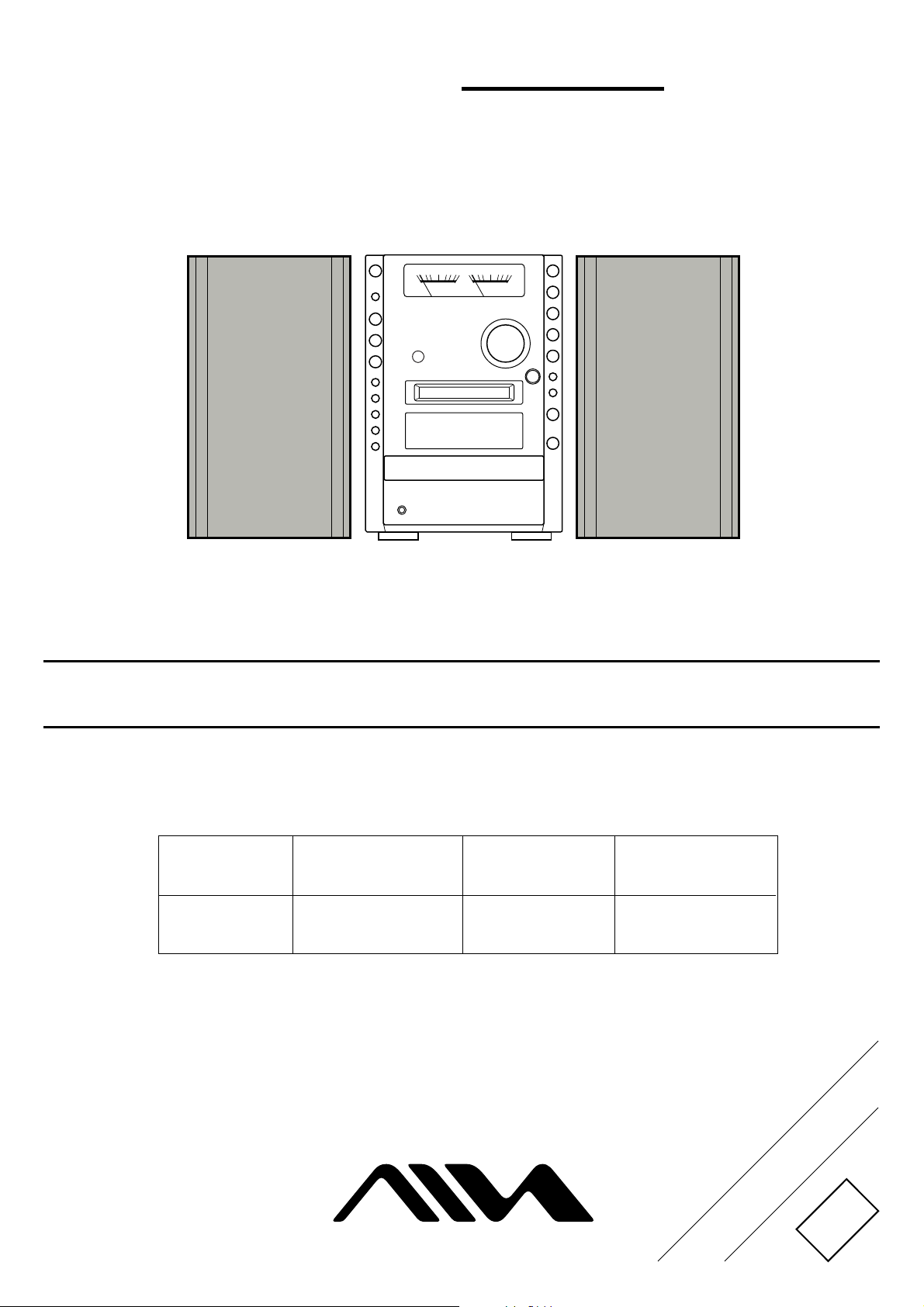
MICRO Hi-Fi COMPONENT SYSTEM
This Service Manual is “Revision Piblishing” and replaces “Simple Manual”
(S/M Code No. 09-032-365-9T2).
CENTER UNIT
XR-FD55
BASIC CD MECHANISM : 3ZG-3 E14NC
BASIC MD MECHANISM : MDM-16QA
SPEAKERSYSTEM
SX-LFD55CX-LFD55
REMOTE
CONTROLLER
RC-CAS20
S/M Code No. 09-032-365-9R2
REVISION
DA T A
Page 2

TABLE OF CONTENTS -1/1
PRECAUTION TO REPLACE OPTICAL BLOCK ..................................................................................................................................... 3
SPECIFICATIONS .................................................................................................................................................................................... 4
ACCESSORIES PARTS LIST .................................................................................................................................................................. 5
ELECTRICAL PARTS LIST ............................................................................................................................................................ 6 ~ 21
TRANSISTOR ILLUSTRATION ............................................................................................................................................................. 21
BLOCK DIAGRAM -1/1 (LEVEL SECTION) ........................................................................................................................................... 22
SCHEMATIC DIAGRAM -1/10 (MAIN-1/3 SECTION) ........................................................................................................................... 23
SCHEMATIC DIAGRAM -2/10 (MAIN-2/3 MD AMP SECTION) ............................................................................................................ 24
SCHEMATIC DIAGRAM -3/10 (MAIN-3/3 LEVEL METER SECTION) .................................................................................................. 25
SCHEMATIC DIAGRAM -4/10 (HP SECTION)...................................................................................................................................... 26
WIRING -1/8 (MAIN C.B, HP C.B) .......................................................................................................................................................... 27
SCHEMATIC DIAGRAM -5/10 (AMP SECTION) .................................................................................................................................. 28
WIRING -2/8 (AMP C.B) ......................................................................................................................................................................... 29
SCHEMATIC DIAGRAM -6/10 (USB SECTION) .................................................................................................................................. 30
WIRING -3/8 (USB C.B) .......................................................................................................................................................................... 31
SCHEMATIC DIAGRAM -7/10 (MICON/DECK SECTION)................................................................................................................... 32
SCHEMATIC DIAGRAM -8/10 (KEY/METER/LED SECTION) ............................................................................................................. 33
WIRING -4/8 (MICON C.B/KEY C.B/METER C.B/LED C.B) .................................................................................................................. 34
WIRING -5/8 (DECK C.B/HEAD C.B) ..................................................................................................................................................... 35
SCHEMATIC DIAGRAM -9/10 (CD SECTION) ..................................................................................................................................... 36
WIRING -6/8 (CD C.B) ............................................................................................................................................................................ 37
WIRING -7/8 (CD DRIVE C.B/CD TRAY C.B) ........................................................................................................................................ 38
SCHEMATIC DIAGRAM -10/10 (PT SECTION) .................................................................................................................................... 39
WIRING -8/8 (PT C.B)............................................................................................................................................................................. 40
ELECTRICAL ADJUSTMENT ......................................................................................................................................................... 41 ~ 45
CD TEST MODE ..................................................................................................................................................................................... 46
FL DISPLAY (15-BT-89GINK) ................................................................................................................................................................ 47
IC BLOCK DIAGRAM.................................................................................................................................................................... 48 ~ 50
IC DESCRIPTION .......................................................................................................................................................................... 51 ~ 55
DISASSEMBLY ............................................................................................................................................................................... 56 ~ 60
MECHANICAL EXPLODED VIEW ....................................................................................................................................................... 61
MECHANICAL PARTS LIST ......................................................................................................................................................... 62 ~ 63
COLOR NAME TABLE.......................................................................................................................................................................... 63
TAPE MECHANISM EXPLODED VIEW <BZM-1 AR2NC> ................................................................................................................. 64
TAPE MECHANISM PARTS LIST <BZM-1 AR2NC> .................................................................................................................. 65 ~ 66
CD MECHANISM EXPLODED VIEW <3ZG-3 E14NC> ...................................................................................................................... 67
CD MECHANISM PARTS LIST <3ZG-3 E14NC> ............................................................................................................................... 68
CD MECHANISM EXPLODED VIEW <CZG-8 YA1NC> ..................................................................................................................... 69
CD MECHANISM PARTS LIST <CZG-8 YA1NC> .............................................................................................................................. 70
GENERAL SPEAKER DISASSEMBLY INSTRUCTIONS (FOR REFERENCE) ................................................................................ 71
SPEAKER PARTS LIST (SX-LFD55) ................................................................................................................................................... 72
OTHER PARTS LIST ............................................................................................................................................................................ 73
MD MECHANISM (MDM-16QA) ............................................................................................................................................................. 74
PROTECTION EYES FROM LASER BEAM DURING SERVICING ...................................................................................................... 75
DISASSEMBLY INSTRUCTION ..................................................................................................................................................... 76 ~ 78
ELECTRICAL PARTS LIST ......................................................................................................................................................... 79 ~ 82
TRANSISTOR ILLUSTRATION ............................................................................................................................................................. 82
BLOCK DIAGRAM -1/1 ........................................................................................................................................................................... 83
SCHEMATIC DIAGRAM -1/1 ................................................................................................................................................................. 84
WIRING -1/2............................................................................................................................................................................................ 85
WIRING -2/2............................................................................................................................................................................................ 86
WAVEFORMS................................................................................................................................................................................. 87 ~ 88
ADJUSTMENT .............................................................................................................................................................................. 89 ~ 101
IC BLOCK DIAGRAM................................................................................................................................................................ 102 ~ 103
IC DESCRIPTION ...................................................................................................................................................................... 104 ~ 111
MECHANISM EXPLODED VIEW ....................................................................................................................................................... 112
MECHANISM PARTS LIST................................................................................................................................................................. 113
OTHER PARTS LIST .......................................................................................................................................................................... 114
-2-
Page 3
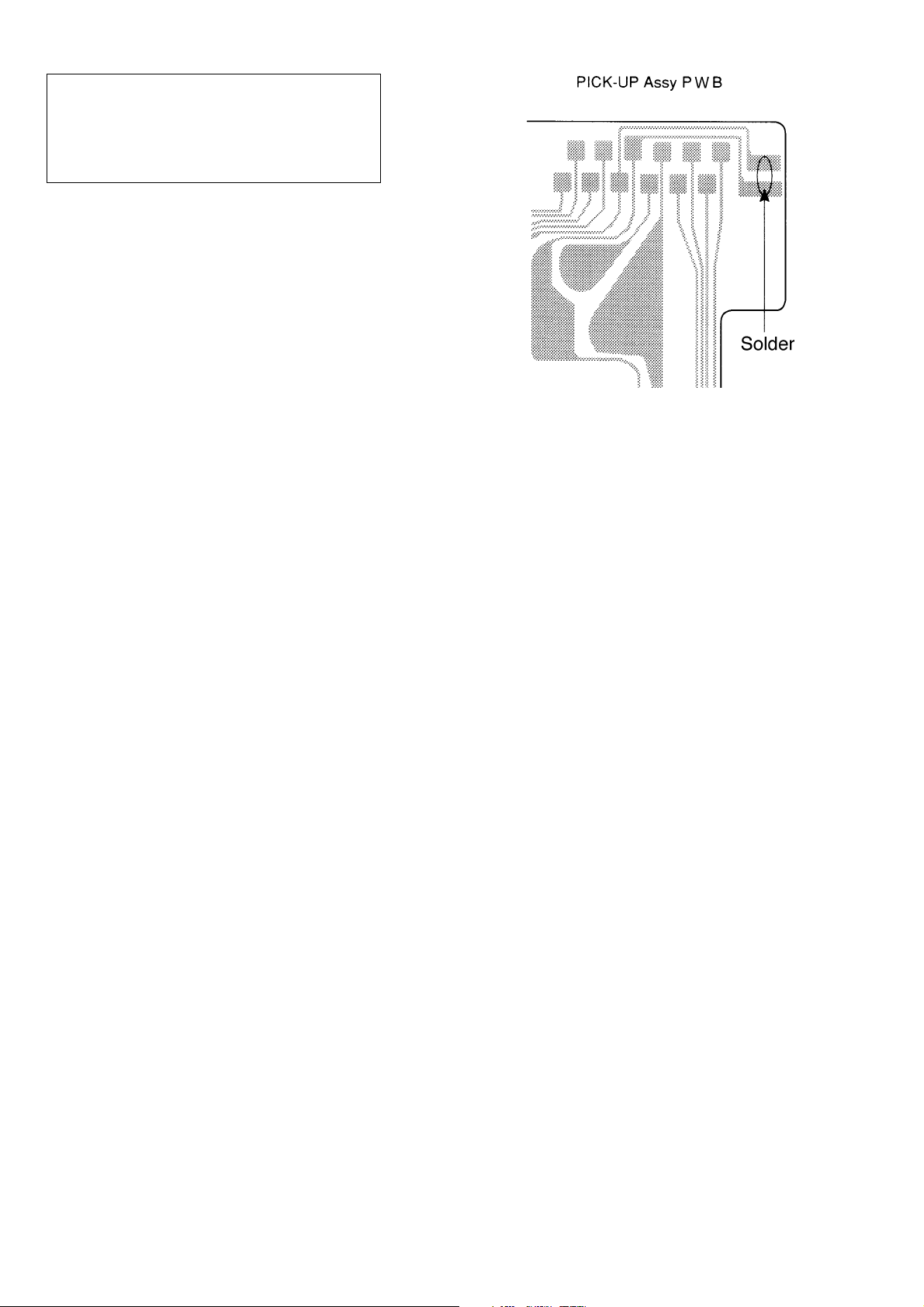
PRECAUTION TO REPLACE OPTICAL BLOCK (PXR-104X-BP-0101)
Body or clothes electrostatic potential could
ruin laser diode in the optical block. Be sure
ground body and workbench, and use care the
clothes do not touch the diode.
1) After the connection, remove solder shown in right figure.
-3-
Page 4

SPECIFICATIONS -1/1
MAIN UNIT CX-LFD55
TUNER
FM tuning range 87.5 MHz to 108 MHz
FM usable sensitivity (IHF) 16.8 dBf
FM antenna terminal 75 Ω (unbalanced)
AM tuning range 531 kHz to 1602 kHz
AM usable sensitivity 350 µV/m
AM antenna Loop antenna
AMPLIFIER
Power output Rated: 24 W + 24 W (6 Ω, T.H.D.1%, 1 kHz/DIN 45500)
Input AUX IN: 800 mV
Outputs SPEAKERS: 6 Ω or more
CD PLAYER
Laser Semiconductor laser ( λ= 780 nm)
Sampling frequency 44.1 kHz
D/A converter 24 bit multi
Frequency 20 to 20000 Hz
Wow and flutter Unmeasurable
MD RECORDER
Scanning method Non-contact optical scanner
Recording system Magnetic polarity modulation overwrite system
Sampling frequency 44.1 kHz
No. of channels Stereo: 2 channels
A/D, D/A converter 1-bit
Frequency 20 to 20000 Hz
Wow and flatter Unmeasurable
Reference: 30 W + 30 W (6 Ω, T.H.D.10%, 1 kHz/DIN 45324)
DIGITAL IN (supported sampling frequencies: 32 kHz, 44.1 kHz and 48 kHz)
PHONES: 32Ω or more
SUB WOOFER: 1.2 V
Emission duration: continuous
(Semiconductor laser application)
Monaural: 1 channel
CASSETTE DECK
Track format 4 tracks, 2 channels stereo
Frequency response Normal tape: 50 Hz to 12500 Hz
Heads Recording/playback x 1, erase x 1
GENERAL
Power requirements 230 V AC, 50 Hz
Power consumption 60 W
Power consumption in standby mode With ECO mode on: 0.5 W
Dimensions (w/h/d) Approx. 155 x 220 x 313.2 mm
Mass Approx. 5.5 kg
With ECO mode off: 17 W
SPEAKER SYSTEM SX-LFD55
Speakers system 2 way, bass-reflex type (magnetic shielded)
Speaker units Woofer: 120 mm cone type
Nominal impedance 6 Ω
Dimensions (w/h/d) Approx. 136 x 220 x 210 mm
Mass Approx. 2.0 kg net per speaker
• Specifications and external appearance are subject to change without notice.
• US AND FOREIGN PATENTS LICENSED FROM DOLBY LABORATORIES.
Tweeter: 25 mm dome type
-4-
Page 5

ACCESSORIES PARTS LIST -1/1
! = ! SAFTY PARTS
C = Components marked
UNIT-NAME ! C REF-NO PARTS-NO PARTS-NAME SUFFIX&MODEL
XR-FD55
CEK
O AS1001 8C-CJE-909-010 IB,K(E)BF XR-FD55 a
O AS1002 87-A92-150-110 ANT,LOOP AM NO-CONT a
O AS1003 87-A92-346-110 ANT,WIRE FM(FASTEN) a
O AS1004 8C-CJE-701-010 RC UNIT,RC-CAS20 a
! O AS1005 87-099-811-110 PLUG,ADPTR CONV(K) a
O AS1006 8B-CPY-610-110 CORD,SPKR 2M a
All components used on this model at the production line are shown in this service manual.
However, please note that not all components will be available as spare parts for after-sales service.
Components marked S and O are designated as spare parts for service and will be stocked at the spare parts centers.
Components marked X and R are not designated as spare parts for after sales service, and will not be stocked at the spare parts centers.
-5-
Page 6

ELECTRICAL PARTS LIST - 1/16
! = ! SAFTY PARTS
C = Components marked
UNIT-NAME ! C REF-NO PARTS-NO PARTS-NAME SUFFIX&MODEL
XR-FD55
CEK
AMP O C 0597 87-010-831-080 C-CAP,U 0.1-16 Z F GRM a
AMP O C 0598 87-010-831-080 C-CAP,U 0.1-16 Z F GRM a
AMP O C 0601 87-012-277-080 C-CAP,U 1800P-50 K B GRM a
AMP O C 0602 87-012-277-080 C-CAP,U 1800P-50 K B GRM a
AMP O C 0603 87-A13-163-080 CAP,E 0.33-50 M FG a
AMP O C 0604 87-A13-163-080 CAP,E 0.33-50 M FG a
AMP O C 0607 87-010-405-040 CAP,E 10-50 M 11L SME a
AMP O C 0608 87-010-405-040 CAP,E 10-50 M 11L SME a
AMP O C 0609 87-012-195-080 C-CAP,U 100P-50 J CH GRM a
AMP O C 0610 87-012-195-080 C-CAP,U 100P-50 J CH GRM a
AMP O C 0611 87-010-258-040 CAP,E 22-35 M 11L SME a
AMP O C 0612 87-010-258-040 CAP,E 22-35 M 11L SME a
AMP O C 0613 87-012-195-080 C-CAP,U 100P-50 J CH GRM a
AMP O C 0614 87-012-195-080 C-CAP,U 100P-50 J CH GRM a
AMP O C 0615 87-012-195-080 C-CAP,U 100P-50 J CH GRM a
AMP O C 0616 87-012-195-080 C-CAP,U 100P-50 J CH GRM a
AMP O C 0617 87-A12-317-080 C-CAP,U 0.1-50 Z F a
AMP O C 0618 87-A12-317-080 C-CAP,U 0.1-50 Z F a
AMP O C 0619 87-012-286-080 C-CAP,U 0.01-25 K B GRM a
AMP O C 0620 87-012-286-080 C-CAP,U 0.01-25 K B GRM a
XR-FD55
CEK
AMP O C 0621 87-A13-165-080 CAP,E 1-50 M FG a
AMP O C 0622 87-A13-165-080 CAP,E 1-50 M FG a
AMP O C 0623 87-010-177-080 C-CAP,S 820P-50 J SL C2012 a
AMP O C 0624 87-010-177-080 C-CAP,S 820P-50 J SL C2012 a
AMP O C 0633 87-012-282-080 C-CAP,U 4700P-50 K B GRM a
AMP O C 0640 87-012-278-080 C-CAP,U 2200P-50 K B GRM a
AMP O C 0686 87-010-759-080 C-CAP,U 0.1-25 Z F CM/CB a
AMP O C 0687 87-010-392-040 CAP,E 33-35 M 11L SME a
AMP O C 0688 87-010-392-040 CAP,E 33-35 M 11L SME a
AMP X CLP0601 87-A60-884-010 PIN,DIA1 COATING-SHS a
AMP O CN 0601 87-A61-013-010 CONN,15P H BLK TAC-L15P-A3 a
AMP O D 0562 87-A40-270-040 C-DIODE,MC2838 a
AMP O D 0565 87-A40-269-040 C-DIODE,MC2836 a
AMP O D 0601 87-A40-269-040 C-DIODE,MC2836 a
AMP O D 0603 87-020-465-080 DIODE,1SS133 a
AMP O D 0604 87-020-465-080 DIODE,1SS133 a
AMP O D 0605 87-A40-269-040 C-DIODE,MC2836 a
AMP O D 0606 87-A40-269-040 C-DIODE,MC2836 a
AMP O D 0607 87-A40-270-040 C-DIODE,MC2838 a
AMP O D 0608 87-A40-270-040 C-DIODE,MC2838 a
XR-FD55
CEK
AMP O D 0617 87-A40-488-080 DIODE,1SS244 a
AMP O D 0618 87-A40-488-080 DIODE,1SS244 a
AMP O D 0650 87-A40-270-040 C-DIODE,MC2838 a
AMP O D 0660 87-A40-270-040 C-DIODE,MC2838 a
AMP O D 0661 87-A40-459-090 DIODE,RL203GW (15MM) a
AMP O D 0662 87-A40-459-090 DIODE,RL203GW (15MM) a
AMP O D 0687 87-A40-747-080 ZENER,UZ5.1BSB a
AMP O D 0688 87-A40-749-080 ZENER,UZ5.6BSB a
AMP O D 0689 87-A40-270-040 C-DIODE,MC2838 a
AMP O D 0690 87-A40-269-040 C-DIODE,MC2836 a
AMP O D 0691 87-A40-764-080 ZENER,UZ10BSC a
AMP O D 0692 87-020-465-080 DIODE,1SS133 a
AMP O D 0693 87-020-465-080 DIODE,1SS133 a
AMP O Q 0539 87-A30-669-040 C-TR,SBT5401 a
AMP O Q 0565 87-A30-538-040 C-TR,SRA2202S a
AMP O Q 0601 87-A30-675-040 C-TR,2SD1306NE07TL a
AMP O Q 0602 87-A30-675-040 C-TR,2SD1306NE07TL a
AMP O Q 0603 87-A30-075-040 C-TR,2SA1235F a
AMP O Q 0604 87-A30-075-040 C-TR,2SA1235F a
AMP O Q 0605 87-A30-075-040 C-TR,2SA1235F a
XR-FD55
CEK
AMP O Q 0606 87-A30-075-040 C-TR,2SA1235F a
AMP O Q 0607 87-A30-076-040 C-TR,2SC3052F a
AMP O Q 0608 87-A30-076-040 C-TR,2SC3052F a
AMP O Q 0609 87-A30-076-040 C-TR,2SC3052F a
AMP O Q 0610 87-A30-076-040 C-TR,2SC3052F a
AMP O Q 0611 87-A30-672-080 TR,2N5551C a
AMP O Q 0612 87-A30-672-080 TR,2N5551C a
AMP O Q 0613 87-A30-076-040 C-TR,2SC3052F a
AMP O Q 0614 87-A30-076-040 C-TR,2SC3052F a
AMP O Q 0615 87-A30-670-040 C-TR,SBT5551 a
AMP O Q 0616 87-A30-670-040 C-TR,SBT5551 a
AMP O Q 0617 87-A30-255-010 TR,2SB1342 a
AMP O Q 0618 87-A30-255-010 TR,2SB1342 a
AMP O Q 0619 87-A30-256-010 TR,2SD1933 a
AMP O Q 0620 87-A30-256-010 TR,2SD1933 a
AMP O Q 0623 87-A30-669-040 C-TR,SBT5401 a
AMP O Q 0624 87-A30-669-040 C-TR,SBT5401 a
AMP O Q 0626 87-A30-669-040 C-TR,SBT5401 a
AMP O Q 0627 87-A30-076-040 C-TR,2SC3052F a
AMP O Q 0628 87-A30-076-040 C-TR,2SC3052F a
All components used on this model at the production line are shown in this service manual.
However, please note that not all components will be available as spare parts for after-sales service.
Components marked S and O are designated as spare parts for service and will be stocked at the spare parts centers.
Components marked X and R are not designated as spare parts for after sales service, and will not be stocked at the spare parts centers.
-6-
Page 7

ELECTRICAL PARTS LIST - 2/16
! = ! SAFTY PARTS
C = Components marked
UNIT-NAME ! C REF-NO PARTS-NO PARTS-NAME SUFFIX&MODEL
XR-FD55
CEK
AMP O Q 0630 87-A30-670-040 C-TR,SBT5551 a
AMP O Q 0683 87-A30-162-010 FET,2SK2937 a
AMP O Q 0684 87-A30-162-010 FET,2SK2937 a
AMP O Q 0685 87-A30-076-040 C-TR,2SC3052F a
AMP O Q 0686 87-A30-075-040 C-TR,2SA1235F a
AMP O Q 0687 87-A30-075-040 C-TR,2SA1235F a
AMP O Q 0735 87-A30-075-040 C-TR,2SA1235F a
AMP O R 0552 88-108-223-080 C-RES,U 22K-1/16W J a
AMP X R 0557 88-108-222-080 C-RES,U 2.2K-1/16W J a
AMP O R 0559 88-118-103-080 C-RES,S 10K-1/10W J a
AMP O R 0560 88-118-473-080 C-RES,S 47K-1/10W J a
AMP O R 0568 88-108-224-080 C-RES,U 220K-1/16W J a
AMP O R 0569 88-108-224-080 C-RES,U 220K-1/16W J a
AMP O R 0571 88-108-473-080 C-RES,U 47K-1/16W J a
AMP O R 0572 88-108-473-080 C-RES,U 47K-1/16W J a
AMP O R 0582 88-130-272-080 RES,2.7K-1/4W J a
AMP O R 0583 88-130-272-080 RES,2.7K-1/4W J a
AMP X R 0601 88-108-392-080 C-RES,U 3.9K-1/16W J a
AMP X R 0602 88-108-392-080 C-RES,U 3.9K-1/16W J a
AMP O R 0603 88-108-153-080 C-RES,U 15K-1/16W J a
XR-FD55
CEK
AMP O R 0604 88-108-153-080 C-RES,U 15K-1/16W J a
AMP O R 0605 88-108-223-080 C-RES,U 22K-1/16W J a
AMP O R 0606 88-108-223-080 C-RES,U 22K-1/16W J a
AMP O R 0607 88-108-101-080 C-RES,U 100-1/16W J a
AMP O R 0608 88-108-101-080 C-RES,U 100-1/16W J a
AMP O R 0611 88-118-102-080 C-RES,S 1K-1/10W J a
AMP O R 0612 88-118-102-080 C-RES,S 1K-1/10W J a
AMP O R 0613 88-118-223-080 C-RES,S 22K-1/10W J a
AMP O R 0614 88-118-223-080 C-RES,S 22K-1/10W J a
AMP O R 0617 88-108-103-080 C-RES,U 10K-1/16W J a
AMP O R 0618 88-108-103-080 C-RES,U 10K-1/16W J a
AMP X R 0619 88-118-101-080 C-RES,S 100-1/10W J a
AMP X R 0620 88-118-101-080 C-RES,S 100-1/10W J a
AMP X R 0621 88-118-101-080 C-RES,S 100-1/10W J a
AMP X R 0622 88-118-101-080 C-RES,S 100-1/10W J a
AMP O R 0623 88-121-222-080 RES,2.2K-1/8W J a
AMP O R 0624 88-121-222-080 RES,2.2K-1/8W J a
AMP O R 0625 88-121-222-080 RES,2.2K-1/8W J a
AMP O R 0626 88-121-222-080 RES,2.2K-1/8W J a
AMP X R 0627 88-118-390-080 C-RES,S 39-1/10W J a
XR-FD55
CEK
AMP X R 0628 88-118-390-080 C-RES,S 39-1/10W J a
AMP O R 0629 87-A00-258-080 RES,M/F 0.22-1W J a
AMP O R 0630 87-A00-258-080 RES,M/F 0.22-1W J a
AMP O R 0631 87-A00-258-080 RES,M/F 0.22-1W J a
AMP O R 0632 87-A00-258-080 RES,M/F 0.22-1W J a
AMP O R 0633 88-108-332-080 C-RES,U 3.3K-1/16W J a
AMP O R 0634 88-108-332-080 C-RES,U 3.3K-1/16W J a
AMP X R 0635 88-108-152-080 C-RES,U 1.5K-1/16W J a
AMP X R 0636 88-108-152-080 C-RES,U 1.5K-1/16W J a
AMP O R 0637 88-108-101-080 C-RES,U 100-1/16W J a
AMP O R 0638 88-108-101-080 C-RES,U 100-1/16W J a
AMP O R 0641 88-118-102-080 C-RES,S 1K-1/10W J a
AMP O R 0642 88-118-102-080 C-RES,S 1K-1/10W J a
AMP O R 0651 88-108-473-080 C-RES,U 47K-1/16W J a
AMP O R 0652 88-108-473-080 C-RES,U 47K-1/16W J a
AMP X R 0655 88-108-682-080 C-RES,U 6.8K-1/16W J a
AMP X R 0656 88-108-682-080 C-RES,U 6.8K-1/16W J a
AMP X R 0657 88-108-472-080 C-RES,U 4.7K-1/16W J a
AMP X R 0658 88-108-472-080 C-RES,U 4.7K-1/16W J a
AMP O R 0659 88-108-103-080 C-RES,U 10K-1/16W J a
XR-FD55
CEK
AMP O R 0660 88-118-103-080 C-RES,S 10K-1/10W J a
AMP X R 0661 88-108-472-080 C-RES,U 4.7K-1/16W J a
AMP X R 0662 88-108-472-080 C-RES,U 4.7K-1/16W J a
AMP X R 0663 88-108-472-080 C-RES,U 4.7K-1/16W J a
AMP X R 0664 88-108-472-080 C-RES,U 4.7K-1/16W J a
AMP X R 0665 88-108-152-080 C-RES,U 1.5K-1/16W J a
AMP X R 0666 88-108-152-080 C-RES,U 1.5K-1/16W J a
AMP O R 0667 88-108-103-080 C-RES,U 10K-1/16W J a
AMP O R 0668 88-118-473-080 C-RES,S 47K-1/10W J a
AMP O R 0671 88-118-182-080 C-RES,S 1.8K-1/10W J a
AMP O R 0672 88-118-182-080 C-RES,S 1.8K-1/10W J a
AMP X R 0673 88-118-222-080 C-RES,S 2.2K-1/10W J a
AMP X R 0674 88-118-222-080 C-RES,S 2.2K-1/10W J a
AMP O R 0675 88-118-331-080 C-RES,S 330-1/10W J a
AMP O R 0676 88-118-331-080 C-RES,S 330-1/10W J a
AMP X R 0677 88-128-222-080 C-RES, 2.2K-1/8W J a
AMP O R 0678 88-118-103-080 C-RES,S 10K-1/10W J a
AMP O R 0679 88-108-102-080 C-RES,U 1K-1/16W J a
AMP O R 0680 88-108-102-080 C-RES,U 1K-1/16W J a
AMP X R 0681 88-118-222-080 C-RES,S 2.2K-1/10W J a
All components used on this model at the production line are shown in this service manual.
However, please note that not all components will be available as spare parts for after-sales service.
Components marked S and O are designated as spare parts for service and will be stocked at the spare parts centers.
Components marked X and R are not designated as spare parts for after sales service, and will not be stocked at the spare parts centers.
-7-
Page 8

ELECTRICAL PARTS LIST - 3/16
! = ! SAFTY PARTS
C = Components marked
UNIT-NAME ! C REF-NO PARTS-NO PARTS-NAME SUFFIX&MODEL
XR-FD55
CEK
AMP X R 0682 88-118-222-080 C-RES,S 2.2K-1/10W J a
AMP O R 0684 88-118-102-080 C-RES,S 1K-1/10W J a
AMP O R 0685 88-108-332-080 C-RES,U 3.3K-1/16W J a
AMP X R 0686 88-118-222-080 C-RES,S 2.2K-1/10W J a
AMP O R 0687 88-118-103-080 C-RES,S 10K-1/10W J a
AMP O R 0688 88-118-102-080 C-RES,S 1K-1/10W J a
AMP X R 0689 88-128-272-080 C-RES, 2.7K-1/8W J a
AMP X R 0690 88-128-272-080 C-RES, 2.7K-1/8W J a
AMP X R 0692 88-128-222-080 C-RES, 2.2K-1/8W J a
AMP O R 0693 88-108-103-080 C-RES,U 10K-1/16W J a
AMP O R 0694 88-108-103-080 C-RES,U 10K-1/16W J a
AMP O R 0695 88-108-473-080 C-RES,U 47K-1/16W J a
AMP O R 0696 88-108-473-080 C-RES,U 47K-1/16W J a
AMP O R 0697 88-108-473-080 C-RES,U 47K-1/16W J a
AMP O R 0698 88-108-473-080 C-RES,U 47K-1/16W J a
AMP X R 0699 88-108-225-080 C-RES,U 2.2M-1/16W J a
AMP X R 0700 88-128-272-080 C-RES, 2.7K-1/8W J a
AMP X R 0713 88-118-563-080 C-RES,S 56K-1/10W J a
AMP O R 0717 88-118-683-080 C-RES,S 68K-1/10W J a
AMP X R 0718 88-118-105-080 C-RES,S 1M-1/10W J a
XR-FD55
CEK
AMP O R 0719 88-108-103-080 C-RES,U 10K-1/16W J a
AMP O TH 0601 87-A91-042-080 C-THMS,100K 55001 a
AMP O TH 0602 87-A91-042-080 C-THMS,100K 55001 a
CD O C 0501 87-A13-118-080 CAP,E 47-16 M RA 6.3X5L a
CD O C 0502 87-010-831-080 C-CAP,U 0.1-16 Z F GRM a
CD O C 0503 87-A13-118-080 CAP,E 47-16 M RA 6.3X5L a
CD O C 0504 87-A13-118-080 CAP,E 47-16 M RA 6.3X5L a
CD O C 0505 87-010-831-080 C-CAP,U 0.1-16 Z F GRM a
CD O C 0506 87-A13-118-080 CAP,E 47-16 M RA 6.3X5L a
CD O C 0507 87-012-274-080 C-CAP,U 1000P-50 K B GRM a
CD O C 0510 87-012-176-080 C-CAP,U 15P-50 J CH GRM a
CD O C 0511 87-012-180-080 C-CAP,U 22P-50 J CH GRM a
CD O C 0513 87-A10-827-080 C-CAP,U 0.47-6.3 K B a
CD O C 0514 87-A10-260-080 C-CAP,U 0.1-16 K B a
CD O C 0515 87-A11-228-080 C-CAP,U 0.027-25 K B a
CD O C 0516 87-A11-228-080 C-CAP,U 0.027-25 K B a
CD O C 0517 87-012-283-080 C-CAP,U 5600P-50 K B GRM a
CD O C 0518 87-012-277-080 C-CAP,U 1800P-50 K B GRM a
CD O C 0519 87-012-279-080 C-CAP,U 2700P-50 K B GRM a
CD O C 0520 87-012-278-080 C-CAP,U 2200P-50 K B GRM a
XR-FD55
CEK
CD O C 0521 87-012-270-080 C-CAP,U 470P-50 K B GRM a
CD O C 0522 87-012-199-080 C-CAP,U 220P-50 J CH GRM a
CD O C 0523 87-012-275-080 C-CAP,U 1200P-50 K B GRM a
CD O C 0524 87-012-193-080 C-CAP,U 82P-50 J CH GRM a
CD O C 0525 87-012-193-080 C-CAP,U 82P-50 J CH GRM a
CD O C 0551 87-A13-120-080 CAP,E 220-10 M RA 8X5L a
CD O C 0553 87-010-831-080 C-CAP,U 0.1-16 Z F GRM a
CD O C 0554 87-A13-118-080 CAP,E 47-16 M RA 6.3X5L a
CD O C 0555 87-010-831-080 C-CAP,U 0.1-16 Z F GRM a
CD O C 0601 87-A13-120-080 CAP,E 220-10 M RA 8X5L a
CD O C 0602 87-010-831-080 C-CAP,U 0.1-16 Z F GRM a
CD O C 0603 87-A13-120-080 CAP,E 220-10 M RA 8X5L a
CD O C 0604 87-010-831-080 C-CAP,U 0.1-16 Z F GRM a
CD O C 0605 87-010-831-080 C-CAP,U 0.1-16 Z F GRM a
CD O C 0606 87-A13-118-080 CAP,E 47-16 M RA 6.3X5L a
CD O C 0607 87-010-831-080 C-CAP,U 0.1-16 Z F GRM a
CD O C 0609 87-A10-047-080 C-CAP,U 1-10 Z F a
CD O C 0614 87-010-831-080 C-CAP,U 0.1-16 Z F GRM a
CD O C 0615 87-012-270-080 C-CAP,U 470P-50 K B GRM a
CD O C 0616 87-010-831-080 C-CAP,U 0.1-16 Z F GRM a
XR-FD55
CEK
CD O C 0617 87-010-784-080 C-CAP,U 0.012-25 K B GRM a
CD O C 0618 87-012-274-080 C-CAP,U 1000P-50 K B GRM a
CD O C 0619 87-A11-058-080 C-CAP,U 0.22-10 K B a
CD X C 0620 88-108-000-080 C-JUMPER,U a
CD O C 0622 87-012-274-080 C-CAP,U 1000P-50 K B GRM a
CD O C 0623 87-A10-260-080 C-CAP,U 0.1-16 K B a
CD O C 0624 87-012-165-080 C-CAP,U 3P-50 C CH GRM a
CD O C 0625 87-012-165-080 C-CAP,U 3P-50 C CH GRM a
CD O C 0626 87-010-831-080 C-CAP,U 0.1-16 Z F GRM a
CD O C 0627 87-010-831-080 C-CAP,U 0.1-16 Z F GRM a
CD O C 0628 87-010-831-080 C-CAP,U 0.1-16 Z F GRM a
CD O C 0629 87-010-831-080 C-CAP,U 0.1-16 Z F GRM a
CD O C 0630 87-012-280-080 C-CAP,U 3300P-50 K B GRM a
CD O C 0631 87-A10-827-080 C-CAP,U 0.47-6.3 K B a
CD O C 0651 87-012-270-080 C-CAP,U 470P-50 K B GRM a
CD O C 0652 87-012-270-080 C-CAP,U 470P-50 K B GRM a
CD O C 0653 87-A13-114-080 CAP,E 2.2-50 M RA 4X5L a
CD O C 0654 87-A13-114-080 CAP,E 2.2-50 M RA 4X5L a
CD O C 0655 87-012-274-080 C-CAP,U 1000P-50 K B GRM a
CD O C 0656 87-012-274-080 C-CAP,U 1000P-50 K B GRM a
All components used on this model at the production line are shown in this service manual.
However, please note that not all components will be available as spare parts for after-sales service.
Components marked S and O are designated as spare parts for service and will be stocked at the spare parts centers.
Components marked X and R are not designated as spare parts for after sales service, and will not be stocked at the spare parts centers.
-8-
Page 9

ELECTRICAL PARTS LIST - 4/16
! = ! SAFTY PARTS
C = Components marked
UNIT-NAME ! C REF-NO PARTS-NO PARTS-NAME SUFFIX&MODEL
XR-FD55
CEK
CD O C 0671 87-A13-118-080 CAP,E 47-16 M RA 6.3X5L a
CD O C 0672 87-010-831-080 C-CAP,U 0.1-16 Z F GRM a
CD O C 0673 87-010-831-080 C-CAP,U 0.1-16 Z F GRM a
CD O C 0674 87-A13-116-080 CAP,E 10-35 M RA 5X5L a
CD O C 0681 87-012-172-080 C-CAP,U 10P-50 D CH GRM a
CD O C 0682 87-012-195-080 C-CAP,U 100P-50 J CH GRM a
CD O C 0683 87-012-188-080 C-CAP,U 47P-50 J CH GRM a
CD O C 0684 87-012-195-080 C-CAP,U 100P-50 J CH GRM a
CD O C 0685 87-012-195-080 C-CAP,U 100P-50 J CH GRM a
CD O C 0686 87-012-195-080 C-CAP,U 100P-50 J CH GRM a
CD O C 0687 87-012-195-080 C-CAP,U 100P-50 J CH GRM a
CD O C 0691 87-010-831-080 C-CAP,U 0.1-16 Z F GRM a
CD O C 0692 87-010-831-080 C-CAP,U 0.1-16 Z F GRM a
CD O C 0694 87-010-831-080 C-CAP,U 0.1-16 Z F GRM a
CD O C 0695 87-018-098-080 CAP,TC U 3.3P-50 K SL UP050 a
CD O C 0696 87-018-098-080 CAP,TC U 3.3P-50 K SL UP050 a
CD O C 0697 87-018-098-080 CAP,TC U 3.3P-50 K SL UP050 a
CD O C 0698 87-A11-148-080 CAP,TC U 0.1-50 Z F a
CD O C 0699 87-A11-148-080 CAP,TC U 0.1-50 Z F a
CD O CN 0501 87-A60-429-010 CONN,16P H TOC-A a
XR-FD55
CEK
CD O CN 0502 87-A60-154-010 CONN,6P H FE a
CD O CN 0503 87-099-210-010 CONN,5P H BLK 6216 a
CD O CN 0601 87-099-030-010 CONN,13P H BLK 6216 a
CD O CN 0602 87-099-200-010 CONN,7P H BLK 6216 a
CD O CN 0603 87-009-348-010 CONN,5P H WHT PH a
CD O D 0551 87-A40-553-080 DIODE,1N4003 LES a
CD O D 0671 87-027-416-080 ZENER,HZ3C2 a
CD X FB 0601 87-003-223-080 F-BEAD,BL02RN2 a
CD X FB 0602 87-003-223-080 F-BEAD,BL02RN2 a
CD O IC 0501 87-A22-373-080 C-IC,AN22002A a
CD O IC 0551 87-A22-280-040 C-IC,BA5813FM a
CD O IC 0601 87-A22-372-030 C-IC,MN6627482WA a
CD O IC 0602 87-017-853-040 C-IC,NJM2100V a
CD O IC 0671 87-A21-993-040 C-IC,PCM1742 KE a
CD O Q 0501 87-A30-075-040 C-TR,2SA1235F a
CD O Q 0502 87-A30-287-040 C-TR,DTC114TKA a
CD O Q 0551 87-A30-495-080 TR,2SA1981Y a
CD O Q 0601 87-A30-283-040 C-TR,DTA114YKA a
CD O Q 0602 87-A30-273-040 C-TR,DTC124EKA a
CD X R 0501 88-108-479-080 C-RES,U 4.7-1/16W J a
XR-FD55
CEK
CD X R 0502 88-108-479-080 C-RES,U 4.7-1/16W J a
CD O R 0503 88-108-101-080 C-RES,U 100-1/16W J a
CD X R 0504 88-108-479-080 C-RES,U 4.7-1/16W J a
CD O R 0505 88-108-822-080 C-RES,U 8.2K-1/16W J a
CD X R 0506 88-108-182-080 C-RES,U 1.8K-1/16W J a
CD O R 0507 88-108-332-080 C-RES,U 3.3K-1/16W J a
CD X R 0510 88-108-154-080 C-RES,U 150K-1/16W J a
CD X R 0511 88-108-394-080 C-RES,U 390K-1/16W J a
CD O R 0512 88-108-223-080 C-RES,U 22K-1/16W J a
CD X R 0513 88-108-104-080 C-RES,U 100K-1/16W J a
CD O R 0514 88-108-333-080 C-RES,U 33K-1/16W J a
CD O R 0515 87-022-235-080 C-RES,U 6.8K-1/16W F a
CD O R 0516 87-022-280-080 C-RES,U 560-1/16W F a
CD O R 0517 87-022-241-080 C-RES,U 12K-1/16W F a
CD X R 0518 88-108-274-080 C-RES,U 270K-1/16W J a
CD X R 0519 88-108-824-080 C-RES,U 820K-1/16W J a
CD O R 0520 87-022-237-080 C-RES,U 8.2K-1/16W F a
CD O R 0521 87-022-237-080 C-RES,U 8.2K-1/16W F a
CD X R 0522 88-108-000-080 C-JUMPER,U a
CD X R 0523 88-108-000-080 C-JUMPER,U a
XR-FD55
CEK
CD X R 0524 88-108-000-080 C-JUMPER,U a
CD X R 0525 88-108-000-080 C-JUMPER,U a
CD X R 0526 88-108-000-080 C-JUMPER,U a
CD O R 0551 88-140-229-080 RES,2.2-1/2W J a
CD O R 0552 88-108-101-080 C-RES,U 100-1/16W J a
CD X R 0553 88-108-222-080 C-RES,U 2.2K-1/16W J a
CD X R 0554 88-108-681-080 C-RES,U 680-1/16W J a
CD O R 0555 88-108-333-080 C-RES,U 33K-1/16W J a
CD O R 0556 88-108-562-080 C-RES,U 5.6K-1/16W J a
CD X R 0557 88-108-000-080 C-JUMPER,U a
CD X R 0558 88-108-000-080 C-JUMPER,U a
CD X R 0559 88-108-000-080 C-JUMPER,U a
CD X R 0560 88-108-000-080 C-JUMPER,U a
CD X R 0565 88-108-181-080 C-RES,U 180-1/16W J a
CD O R 0566 88-108-821-080 C-RES,U 820-1/16W J a
CD X R 0601 88-108-229-080 C-RES,U 2.2-1/16W J a
CD X R 0602 88-108-339-080 C-RES,U 3.3-1/16W J a
CD X R 0603 88-108-100-080 C-RES,U 10-1/16W J a
CD X R 0604 88-108-000-080 C-JUMPER,U a
CD X R 0605 88-108-000-080 C-JUMPER,U a
All components used on this model at the production line are shown in this service manual.
However, please note that not all components will be available as spare parts for after-sales service.
Components marked S and O are designated as spare parts for service and will be stocked at the spare parts centers.
Components marked X and R are not designated as spare parts for after sales service, and will not be stocked at the spare parts centers.
-9-
Page 10

ELECTRICAL PARTS LIST - 5/16
! = ! SAFTY PARTS
C = Components marked
UNIT-NAME ! C REF-NO PARTS-NO PARTS-NAME SUFFIX&MODEL
XR-FD55
CEK
CD O R 0608 88-108-473-080 C-RES,U 47K-1/16W J a
CD O R 0610 88-108-123-080 C-RES,U 12K-1/16W J a
CD O R 0611 88-108-102-080 C-RES,U 1K-1/16W J a
CD X R 0612 88-108-000-080 C-JUMPER,U a
CD O R 0613 88-108-473-080 C-RES,U 47K-1/16W J a
CD X R 0614 88-108-000-080 C-JUMPER,U a
CD O R 0616 88-108-153-080 C-RES,U 15K-1/16W J a
CD O R 0617 88-108-272-080 C-RES,U 2.7K-1/16W J a
CD X R 0618 88-108-000-080 C-JUMPER,U a
CD O R 0619 88-108-102-080 C-RES,U 1K-1/16W J a
CD O R 0620 88-108-103-080 C-RES,U 10K-1/16W J a
CD X R 0621 88-108-105-080 C-RES,U 1M-1/16W J a
CD X R 0622 88-108-475-080 C-RES,U 4.7M-1/16W J a
CD X R 0623 88-108-104-080 C-RES,U 100K-1/16W J a
CD X R 0624 88-108-104-080 C-RES,U 100K-1/16W J a
CD O R 0625 88-108-333-080 C-RES,U 33K-1/16W J a
CD X R 0626 88-108-331-080 C-RES,U 330-1/16W J a
CD O R 0628 88-108-474-080 C-RES,U 470K-1/16W J a
CD X R 0629 88-108-221-080 C-RES,U 220-1/16W J a
CD X R 0631 88-108-220-080 C-RES,U 22-1/16W J a
XR-FD55
CEK
CD X R 0632 88-108-000-080 C-JUMPER,U a
CD X R 0633 88-108-104-080 C-RES,U 100K-1/16W J a
CD X R 0634 88-108-000-080 C-JUMPER,U a
CD O R 0635 88-108-103-080 C-RES,U 10K-1/16W J a
CD X R 0636 88-108-000-080 C-JUMPER,U a
CD X R 0637 88-108-000-080 C-JUMPER,U a
CD X R 0638 88-108-000-080 C-JUMPER,U a
CD X R 0639 88-108-000-080 C-JUMPER,U a
CD X R 0640 88-108-000-080 C-JUMPER,U a
CD X R 0641 88-108-000-080 C-JUMPER,U a
CD O R 0642 88-108-473-080 C-RES,U 47K-1/16W J a
CD X R 0643 88-108-393-080 C-RES,U 39K-1/16W J a
CD X R 0644 88-108-393-080 C-RES,U 39K-1/16W J a
CD X R 0645 88-108-104-080 C-RES,U 100K-1/16W J a
CD O R 0646 88-108-272-080 C-RES,U 2.7K-1/16W J a
CD O R 0647 88-108-683-080 C-RES,U 68K-1/16W J a
CD O R 0648 88-108-103-080 C-RES,U 10K-1/16W J a
CD O R 0649 88-108-103-080 C-RES,U 10K-1/16W J a
CD X R 0653 88-108-152-080 C-RES,U 1.5K-1/16W J a
CD X R 0654 88-108-152-080 C-RES,U 1.5K-1/16W J a
XR-FD55
CEK
CD O R 0655 88-108-102-080 C-RES,U 1K-1/16W J a
CD O R 0656 88-108-102-080 C-RES,U 1K-1/16W J a
CD O R 0657 88-108-103-080 C-RES,U 10K-1/16W J a
CD O R 0658 88-108-103-080 C-RES,U 10K-1/16W J a
CD X R 0659 88-108-000-080 C-JUMPER,U a
CD X R 0660 88-108-000-080 C-JUMPER,U a
CD O R 0671 88-108-101-080 C-RES,U 100-1/16W J a
CD O R 0681 88-108-101-080 C-RES,U 100-1/16W J a
CD O R 0682 88-108-101-080 C-RES,U 100-1/16W J a
CD O R 0683 88-108-101-080 C-RES,U 100-1/16W J a
CD O R 0684 88-108-101-080 C-RES,U 100-1/16W J a
CD O R 0685 88-108-101-080 C-RES,U 100-1/16W J a
CD O R 0686 88-108-101-080 C-RES,U 100-1/16W J a
CD O R 0687 88-108-101-080 C-RES,U 100-1/16W J a
CD X R 0688 88-108-000-080 C-JUMPER,U a
CD X R 0689 88-108-000-080 C-JUMPER,U a
CD X R 0690 88-108-000-080 C-JUMPER,U a
CD X R 0692 88-108-000-080 C-JUMPER,U a
CD X R 0693 88-108-000-080 C-JUMPER,U a
CD X R 0695 88-108-222-080 C-RES,U 2.2K-1/16W J a
XR-FD55
CEK
CD X R 0697 88-108-000-080 C-JUMPER,U a
CD X W 0602 8C-CJE-661-010 WIRE ASSY,120 BLACK FASTON a
CD O X 0602 87-A70-363-010 VIB,XTAL 16.9344MHZ CSA-309 a
HP O C 0223 87-012-272-080 C-CAP,U 680P-50 K B GRM a
HP O C 0224 87-012-272-080 C-CAP,U 680P-50 K B GRM a
HP X C 0230 87-A11-120-080 CAP,TC U 2200P-50 J CH a
HP X C 0231 87-A11-120-080 CAP,TC U 2200P-50 J CH a
HP O CNA0201 8C-CJE-603-010 CONN ASSY,5P TID-A300 a
HP O J 0201 87-A61-821-010 JACK,3.5 BLK ST W/SW GLD a
HP X R 0243 88-130-151-080 RES,150-1/4W J a
HP X R 0244 88-130-151-080 RES,150-1/4W J a
HP X R 0245 88-130-151-080 RES,150-1/4W J a
HP X R 0246 88-130-151-080 RES,150-1/4W J a
HP O R 0265 88-121-222-080 RES,2.2K-1/8W J a
HP O R 0266 88-121-222-080 RES,2.2K-1/8W J a
HP O WH 0101 87-A90-459-010 HLDR,WIRE 2.5-5P a
KEY O C 0101 87-010-831-080 C-CAP,U 0.1-16 Z F GRM a
KEY O C 0102 87-010-831-080 C-CAP,U 0.1-16 Z F GRM a
KEY O C 0103 87-015-698-040 CAP,E 4.7-50 M 7L SRA a
KEY O C 0104 87-015-698-040 CAP,E 4.7-50 M 7L SRA a
All components used on this model at the production line are shown in this service manual.
However, please note that not all components will be available as spare parts for after-sales service.
Components marked S and O are designated as spare parts for service and will be stocked at the spare parts centers.
Components marked X and R are not designated as spare parts for after sales service, and will not be stocked at the spare parts centers.
-10-
Page 11

ELECTRICAL PARTS LIST - 6/16
! = ! SAFTY PARTS
C = Components marked
UNIT-NAME ! C REF-NO PARTS-NO PARTS-NAME SUFFIX&MODEL
XR-FD55
CEK
KEY O C 0105 87-010-408-040 CAP,E 47-50 M 11L SME a
KEY O C 0106 87-A12-317-080 C-CAP,U 0.1-50 Z F a
KEY O C 0114 87-015-699-040 CAP,E 10-50 M 7L SRA a
KEY O C 0115 87-012-274-080 C-CAP,U 1000P-50 K B GRM a
KEY O C 0117 87-012-286-080 C-CAP,U 0.01-25 K B GRM a
KEY O C 0118 87-012-286-080 C-CAP,U 0.01-25 K B GRM a
KEY O C 0120 87-012-286-080 C-CAP,U 0.01-25 K B GRM a
KEY O C 0121 87-012-286-080 C-CAP,U 0.01-25 K B GRM a
KEY O C 0122 87-A11-088-080 CAP,TC U 100P-50 J CH a
KEY O C 0145 87-012-172-080 C-CAP,U 10P-50 D CH GRM a
KEY O C 0146 87-012-172-080 C-CAP,U 10P-50 D CH GRM a
KEY O C 0147 87-012-172-080 C-CAP,U 10P-50 D CH GRM a
KEY O C 0148 87-012-172-080 C-CAP,U 10P-50 D CH GRM a
KEY O CN 0108 87-099-034-010 CONN,17P H BLK 6216 a
KEY O D 0110 87-A40-269-040 C-DIODE,MC2836 a
KEY O FL 0101 8C-CJE-609-010 FL,15-BT-89GINK a
KEY O IC 0103 87-A22-043-010 IC,SPS-440-1-E1 a
KEY O LED0101 87-A40-317-080 LED,SLR-342VCT31 RED a
KEY O LED0102 87-A41-112-010 LED,SEL2710K YEL a
KEY O Q 0111 87-A30-435-040 C-TR,DTC144EKA a
XR-FD55
CEK
KEY O Q 0113 87-A30-435-040 C-TR,DTC144EKA a
KEY O R 0101 88-118-153-080 C-RES,S 15K-1/10W J a
KEY O R 0102 88-118-153-080 C-RES,S 15K-1/10W J a
KEY X R 0105 88-121-220-080 RES,22-1/8W J a
KEY O R 0106 88-108-821-080 C-RES,U 820-1/16W J a
KEY O R 0108 88-108-821-080 C-RES,U 820-1/16W J a
KEY X R 0110 88-100-000-010 PLATING-JW, 0.58 SN95 a
KEY O R 0136 88-108-102-080 C-RES,U 1K-1/16W J a
KEY O R 0138 88-108-563-080 C-RES,U 56K-1/16W J a
KEY O R 0145 88-108-223-080 C-RES,U 22K-1/16W J a
KEY O R 0146 88-108-223-080 C-RES,U 22K-1/16W J a
KEY X R 0147 88-108-221-080 C-RES,U 220-1/16W J a
KEY O R 0148 88-108-272-080 C-RES,U 2.7K-1/16W J a
KEY O R 0150 88-108-103-080 C-RES,U 10K-1/16W J a
KEY O R 0151 88-108-103-080 C-RES,U 10K-1/16W J a
KEY O R 0157 88-108-103-080 C-RES,U 10K-1/16W J a
KEY O R 0158 88-108-103-080 C-RES,U 10K-1/16W J a
KEY O R 0159 88-108-103-080 C-RES,U 10K-1/16W J a
KEY O R 0160 88-108-103-080 C-RES,U 10K-1/16W J a
KEY O R 0170 88-108-103-080 C-RES,U 10K-1/16W J a
XR-FD55
CEK
KEY O R 0171 88-108-122-080 C-RES,U 1.2K-1/16W J a
KEY O R 0172 88-108-122-080 C-RES,U 1.2K-1/16W J a
KEY X R 0173 88-108-222-080 C-RES,U 2.2K-1/16W J a
KEY X R 0174 88-108-222-080 C-RES,U 2.2K-1/16W J a
KEY O R 0175 88-108-332-080 C-RES,U 3.3K-1/16W J a
KEY X R 0176 88-108-472-080 C-RES,U 4.7K-1/16W J a
KEY O R 0177 88-108-822-080 C-RES,U 8.2K-1/16W J a
KEY O R 0178 88-108-183-080 C-RES,U 18K-1/16W J a
KEY X R 0179 88-108-393-080 C-RES,U 39K-1/16W J a
KEY O R 0212 88-108-103-080 C-RES,U 10K-1/16W J a
KEY O R 0213 88-108-122-080 C-RES,U 1.2K-1/16W J a
KEY O R 0214 88-108-122-080 C-RES,U 1.2K-1/16W J a
KEY X R 0215 88-108-222-080 C-RES,U 2.2K-1/16W J a
KEY X R 0216 88-108-222-080 C-RES,U 2.2K-1/16W J a
KEY O R 0217 88-108-332-080 C-RES,U 3.3K-1/16W J a
KEY X R 0218 88-108-472-080 C-RES,U 4.7K-1/16W J a
KEY O R 0219 88-108-822-080 C-RES,U 8.2K-1/16W J a
KEY O R 0220 88-108-183-080 C-RES,U 18K-1/16W J a
KEY X R 0221 88-108-393-080 C-RES,U 39K-1/16W J a
KEY O S 0101 87-A91-024-180 SW,TACT KSHG611BT a
XR-FD55
CEK
KEY O S 0102 87-A91-024-180 SW,TACT KSHG611BT a
KEY O S 0103 87-A91-024-180 SW,TACT KSHG611BT a
KEY O S 0104 87-A91-024-180 SW,TACT KSHG611BT a
KEY O S 0105 87-A91-024-180 SW,TACT KSHG611BT a
KEY O S 0106 87-A91-024-180 SW,TACT KSHG611BT a
KEY O S 0107 87-A91-024-180 SW,TACT KSHG611BT a
KEY O S 0108 87-A91-024-180 SW,TACT KSHG611BT a
KEY O S 0109 87-A91-024-180 SW,TACT KSHG611BT a
KEY O S 0110 87-A91-024-180 SW,TACT KSHG611BT a
KEY O S 0111 87-A91-024-180 SW,TACT KSHG611BT a
KEY O S 0112 87-A91-024-180 SW,TACT KSHG611BT a
KEY O S 0113 87-A92-419-010 SW,RTRY EC12E24304WITH VC a
KEY O S 0114 87-A91-024-180 SW,TACT KSHG611BT a
KEY O S 0115 87-A91-024-180 SW,TACT KSHG611BT a
KEY O S 0116 87-A91-024-180 SW,TACT KSHG611BT a
KEY O S 0117 87-A91-024-180 SW,TACT KSHG611BT a
KEY O S 0118 87-A91-024-180 SW,TACT KSHG611BT a
KEY O S 0119 87-A91-024-180 SW,TACT KSHG611BT a
KEY O S 0120 87-A91-024-180 SW,TACT KSHG611BT a
KEY O S 0123 87-A90-894-010 SW,RTRY EC12E12444 a
All components used on this model at the production line are shown in this service manual.
However, please note that not all components will be available as spare parts for after-sales service.
Components marked S and O are designated as spare parts for service and will be stocked at the spare parts centers.
Components marked X and R are not designated as spare parts for after sales service, and will not be stocked at the spare parts centers.
-11-
Page 12

ELECTRICAL PARTS LIST - 7/16
! = ! SAFTY PARTS
C = Components marked
UNIT-NAME ! C REF-NO PARTS-NO PARTS-NAME SUFFIX&MODEL
XR-FD55
CEK
LED O C 0130 87-010-831-080 C-CAP,U 0.1-16 Z F GRM a
LED O C 0131 87-010-831-080 C-CAP,U 0.1-16 Z F GRM a
LED O C 0136 87-010-831-080 C-CAP,U 0.1-16 Z F GRM a
LED O C 0138 87-010-831-080 C-CAP,U 0.1-16 Z F GRM a
LED O CN 0106 87-A60-538-010 CONN,5P H TUC-P05X-B1 a
LED O D 0105 87-A40-821-080 LED,SMLS1BE16C BLU/UMB a
LED O D 0106 87-A40-821-080 LED,SMLS1BE16C BLU/UMB a
LED X R 0222 88-108-560-080 C-RES,U 56-1/16W J a
LED O R 0223 88-108-103-080 C-RES,U 10K-1/16W J a
LED O R 0224 88-108-103-080 C-RES,U 10K-1/16W J a
LED X R 0226 88-108-151-080 C-RES,U 150-1/16W J a
LED X R 0227 88-108-560-080 C-RES,U 56-1/16W J a
LED O R 0228 88-108-103-080 C-RES,U 10K-1/16W J a
LED O R 0229 88-108-103-080 C-RES,U 10K-1/16W J a
LED X R 0233 88-108-151-080 C-RES,U 150-1/16W J a
MAIN O C 0001 87-A10-520-000 CAP,E 3300-35 M SMG a
MAIN O C 0002 87-A10-520-000 CAP,E 3300-35 M SMG a
MAIN O C 0003 87-A12-317-080 C-CAP,U 0.1-50 Z F a
MAIN O C 0004 87-A12-317-080 C-CAP,U 0.1-50 Z F a
MAIN O C 0005 87-A12-317-080 C-CAP,U 0.1-50 Z F a
XR-FD55
CEK
MAIN O C 0006 87-A12-317-080 C-CAP,U 0.1-50 Z F a
MAIN O C 0009 87-010-759-080 C-CAP,U 0.1-25 Z F CM/CB a
MAIN O C 0010 87-010-759-080 C-CAP,U 0.1-25 Z F CM/CB a
MAIN O C 0011 87-010-759-080 C-CAP,U 0.1-25 Z F CM/CB a
MAIN O C 0012 87-010-759-080 C-CAP,U 0.1-25 Z F CM/CB a
MAIN O C 0013 87-012-282-080 C-CAP,U 4700P-50 K B GRM a
MAIN O C 0014 87-010-384-040 CAP,E 100-25 M 11L SME a
MAIN O C 0016 87-012-282-080 C-CAP,U 4700P-50 K B GRM a
MAIN O C 0017 87-010-759-080 C-CAP,U 0.1-25 Z F CM/CB a
MAIN O C 0021 87-010-928-000 CAP,E 4700-25 M SMG a
MAIN O C 0022 87-010-928-000 CAP,E 4700-25 M SMG a
MAIN O C 0025 87-010-247-080 CAP,E 100-50 M SME a
MAIN O C 0026 87-010-247-080 CAP,E 100-50 M SME a
MAIN O C 0029 87-010-393-080 CAP,E 100-35 M SME a
MAIN O C 0030 87-010-393-080 CAP,E 100-35 M SME a
MAIN O C 0031 87-010-263-040 CAP,E 100-10 M 11L SME a
MAIN O C 0034 87-010-260-040 CAP,E 47-25 M 11L SME a
MAIN O C 0035 87-010-391-040 CAP,E 10-35 M 11L SME a
MAIN O C 0036 87-010-386-080 CAP,E 330-25 M SME a
MAIN O C 0041 87-010-759-080 C-CAP,U 0.1-25 Z F CM/CB a
XR-FD55
CEK
MAIN O C 0042 87-010-759-080 C-CAP,U 0.1-25 Z F CM/CB a
MAIN O C 0043 87-010-759-080 C-CAP,U 0.1-25 Z F CM/CB a
MAIN O C 0044 87-010-759-080 C-CAP,U 0.1-25 Z F CM/CB a
MAIN O C 0045 87-A12-829-000 CAP,E 4700-25 M 85 GS a
MAIN O C 0051 87-010-759-080 C-CAP,U 0.1-25 Z F CM/CB a
MAIN O C 0053 87-010-252-080 CAP,E 1000-6.3 M SME a
MAIN O C 0060 87-010-403-040 CAP,E 3.3-50 M 11L SME a
MAIN O C 0061 87-010-260-040 CAP,E 47-25 M 11L SME a
MAIN O C 0101 87-012-278-080 C-CAP,U 2200P-50 K B GRM a
MAIN O C 0102 87-012-278-080 C-CAP,U 2200P-50 K B GRM a
MAIN O C 0103 87-015-698-040 CAP,E 4.7-50 M 7L SRA a
MAIN O C 0104 87-015-698-040 CAP,E 4.7-50 M 7L SRA a
MAIN O C 0109 87-015-681-040 CAP,E 10-16 7L SRA a
MAIN O C 0110 87-015-681-040 CAP,E 10-16 7L SRA a
MAIN O C 0111 87-010-831-080 C-CAP,U 0.1-16 Z F GRM a
MAIN O C 0112 87-010-831-080 C-CAP,U 0.1-16 Z F GRM a
MAIN O C 0225 87-A10-307-080 CAP,M 0.1-50 J a
MAIN O C 0226 87-A10-307-080 CAP,M 0.1-50 J a
MAIN O C 0227 87-A10-307-080 CAP,M 0.1-50 J a
MAIN O C 0228 87-A10-307-080 CAP,M 0.1-50 J a
XR-FD55
CEK
MAIN O C 0229 87-010-191-080 C-CAP,S 0.015-50 Z F GRM a
MAIN O C 0230 87-010-191-080 C-CAP,S 0.015-50 Z F GRM a
MAIN O C 0231 87-012-286-080 C-CAP,U 0.01-25 K B GRM a
MAIN O C 0232 87-012-286-080 C-CAP,U 0.01-25 K B GRM a
MAIN O C 0233 87-012-286-080 C-CAP,U 0.01-25 K B GRM a
MAIN O C 0303 87-012-275-080 C-CAP,U 1200P-50 K B GRM a
MAIN O C 0304 87-012-275-080 C-CAP,U 1200P-50 K B GRM a
MAIN O C 0305 87-012-270-080 C-CAP,U 470P-50 K B GRM a
MAIN O C 0363 87-010-831-080 C-CAP,U 0.1-16 Z F GRM a
MAIN O C 0451 87-010-759-080 C-CAP,U 0.1-25 Z F CM/CB a
MAIN O C 0452 87-015-690-040 CAP,E 22-35 M 7L SRA a
MAIN O C 0453 87-012-279-080 C-CAP,U 2700P-50 K B GRM a
MAIN O C 0454 87-012-279-080 C-CAP,U 2700P-50 K B GRM a
MAIN O C 0455 87-012-279-080 C-CAP,U 2700P-50 K B GRM a
MAIN O C 0456 87-012-286-080 C-CAP,U 0.01-25 K B GRM a
MAIN O C 0457 87-A12-361-080 CAP,M 5600P-100 J CP a
MAIN O C 0458 87-012-278-080 C-CAP,U 2200P-50 K B GRM a
MAIN O C 0459 87-012-271-080 C-CAP,U 560P-50 K B GRM a
MAIN O C 0460 87-010-759-080 C-CAP,U 0.1-25 Z F CM/CB a
MAIN O C 0461 87-012-158-080 C-CAP,S 390P-50 J CH GRM a
All components used on this model at the production line are shown in this service manual.
However, please note that not all components will be available as spare parts for after-sales service.
Components marked S and O are designated as spare parts for service and will be stocked at the spare parts centers.
Components marked X and R are not designated as spare parts for after sales service, and will not be stocked at the spare parts centers.
-12-
Page 13

ELECTRICAL PARTS LIST - 8/16
! = ! SAFTY PARTS
C = Components marked
UNIT-NAME ! C REF-NO PARTS-NO PARTS-NAME SUFFIX&MODEL
XR-FD55
CEK
MAIN O C 0462 87-012-158-080 C-CAP,S 390P-50 J CH GRM a
MAIN O C 0463 87-010-831-080 C-CAP,U 0.1-16 Z F GRM a
MAIN O C 0464 87-012-278-080 C-CAP,U 2200P-50 K B GRM a
MAIN O C 0601 87-012-188-080 C-CAP,U 47P-50 J CH GRM a
MAIN O C 0602 87-012-188-080 C-CAP,U 47P-50 J CH GRM a
MAIN O C 0603 87-010-555-040 CAP,E 100-10 M 5L SRE a
MAIN O C 0604 87-010-555-040 CAP,E 100-10 M 5L SRE a
MAIN O C 0605 87-012-284-080 C-CAP,U 6800P-50 K B GRM a
MAIN O C 0606 87-012-284-080 C-CAP,U 6800P-50 K B GRM a
MAIN O C 0607 87-012-273-080 C-CAP,U 820P-50 K B GRM a
MAIN O C 0608 87-012-273-080 C-CAP,U 820P-50 K B GRM a
MAIN O C 0609 87-A13-165-080 CAP,E 1-50 M FG a
MAIN O C 0610 87-A13-165-080 CAP,E 1-50 M FG a
MAIN O C 0613 87-012-274-080 C-CAP,U 1000P-50 K B GRM a
MAIN O C 0614 87-012-274-080 C-CAP,U 1000P-50 K B GRM a
MAIN O C 0615 87-012-274-080 C-CAP,U 1000P-50 K B GRM a
MAIN O C 0616 87-012-274-080 C-CAP,U 1000P-50 K B GRM a
MAIN O C 0617 87-012-286-080 C-CAP,U 0.01-25 K B GRM a
MAIN O C 0618 87-012-286-080 C-CAP,U 0.01-25 K B GRM a
MAIN O C 0619 87-012-286-080 C-CAP,U 0.01-25 K B GRM a
XR-FD55
CEK
MAIN O C 0620 87-012-286-080 C-CAP,U 0.01-25 K B GRM a
MAIN O C 0621 87-010-545-040 CAP,E 0.22-50 M 11L SME a
MAIN O C 0622 87-010-545-040 CAP,E 0.22-50 M 11L SME a
MAIN O C 0623 87-010-545-040 CAP,E 0.22-50 M 11L SME a
MAIN O C 0624 87-010-545-040 CAP,E 0.22-50 M 11L SME a
MAIN O C 0625 87-012-281-080 C-CAP,U 3900P-50 K B GRM a
MAIN O C 0626 87-012-281-080 C-CAP,U 3900P-50 K B GRM a
MAIN O C 0631 87-012-195-080 C-CAP,U 100P-50 J CH GRM a
MAIN O C 0632 87-012-195-080 C-CAP,U 100P-50 J CH GRM a
MAIN O C 0633 87-012-284-080 C-CAP,U 6800P-50 K B GRM a
MAIN O C 0634 87-012-284-080 C-CAP,U 6800P-50 K B GRM a
MAIN O C 0635 87-012-286-080 C-CAP,U 0.01-25 K B GRM a
MAIN O C 0636 87-012-286-080 C-CAP,U 0.01-25 K B GRM a
MAIN O C 0637 87-012-278-080 C-CAP,U 2200P-50 K B GRM a
MAIN O C 0638 87-012-278-080 C-CAP,U 2200P-50 K B GRM a
MAIN O C 0651 87-A13-045-040 CAP,E 220-16 M VR-GSO a
MAIN O C 0652 87-A13-030-040 CAP,E 47-35 M VR-GSO a
MAIN O C 0655 87-012-286-080 C-CAP,U 0.01-25 K B GRM a
MAIN O C 0656 87-012-186-080 C-CAP,U 39P-50 J CH GRM a
MAIN O C 0657 87-012-286-080 C-CAP,U 0.01-25 K B GRM a
XR-FD55
CEK
MAIN O C 0658 87-012-281-080 C-CAP,U 3900P-50 K B GRM a
MAIN O C 0659 87-010-831-080 C-CAP,U 0.1-16 Z F GRM a
MAIN O C 0660 87-010-402-040 CAP,E 2.2-50 M 11L SME a
MAIN O C 0663 87-010-831-080 C-CAP,U 0.1-16 Z F GRM a
MAIN O C 0664 87-010-831-080 C-CAP,U 0.1-16 Z F GRM a
MAIN O C 0667 87-015-684-040 CAP,E 47-16 M 7L SRA a
MAIN O C 0669 87-012-271-080 C-CAP,U 560P-50 K B GRM a
MAIN O C 0670 87-012-271-080 C-CAP,U 560P-50 K B GRM a
MAIN O C 0672 87-010-831-080 C-CAP,U 0.1-16 Z F GRM a
MAIN O C 0676 87-010-831-080 C-CAP,U 0.1-16 Z F GRM a
MAIN O C 0677 87-012-286-080 C-CAP,U 0.01-25 K B GRM a
MAIN O C 0681 87-015-695-040 CAP,E 1-50 7L SRA a
MAIN O C 0682 87-015-695-040 CAP,E 1-50 7L SRA a
MAIN O C 0683 87-010-497-040 CAP,E 4.7-35 M 5L SRE a
MAIN O C 0684 87-015-698-040 CAP,E 4.7-50 M 7L SRA a
MAIN O C 0693 87-010-831-080 C-CAP,U 0.1-16 Z F GRM a
MAIN O C 0694 87-010-831-080 C-CAP,U 0.1-16 Z F GRM a
MAIN O C 0751 87-010-497-040 CAP,E 4.7-35 M 5L SRE a
MAIN O C 0752 87-010-497-040 CAP,E 4.7-35 M 5L SRE a
MAIN O C 0753 87-010-494-040 CAP,E 1-50 M 5L SRE a
XR-FD55
CEK
MAIN O C 0754 87-010-494-040 CAP,E 1-50 M 5L SRE a
MAIN O C 0755 87-010-754-080 CAP,E 220-10 M 7L SRA a
MAIN O C 0756 87-A10-189-040 CAP,E 220-10 M 5L a
MAIN O C 0803 87-010-831-080 C-CAP,U 0.1-16 Z F GRM a
MAIN X CLP0301 87-A60-884-010 PIN,DIA1 COATING-SHS a
MAIN O CN 0101 87-A61-108-010 CONN,5P V TID-A a
MAIN O CN 0302 87-A60-625-010 CONN,8P V 2MM JMT a
MAIN O CN 0601 87-099-394-010 CONN,28P V BLK 6216 a
MAIN O CN 0602 87-099-195-010 CONN,7P V BLK 6216 a
MAIN O CN 0604 87-099-013-010 CONN,11P V BLK 6216 a
MAIN O CN 0605 87-A60-998-010 CONN,15P V BLK TAC-L15X-A3 a
MAIN O CN 0607 87-099-195-010 CONN,7P V BLK 6216 a
MAIN O CN 0608 87-099-014-010 CONN,12P V BLK 6216 a
MAIN O CNA0001 8C-CJE-602-010 CONN ASSY,11P TID-A200 a
MAIN O D 0001 87-A40-455-080 DIODE,RL203 GW a
MAIN O D 0002 87-A40-455-080 DIODE,RL203 GW a
MAIN O D 0003 87-A40-455-080 DIODE,RL203 GW a
MAIN O D 0004 87-A40-455-080 DIODE,RL203 GW a
MAIN O D 0005 87-A40-455-080 DIODE,RL203 GW a
MAIN O D 0006 87-A40-455-080 DIODE,RL203 GW a
All components used on this model at the production line are shown in this service manual.
However, please note that not all components will be available as spare parts for after-sales service.
Components marked S and O are designated as spare parts for service and will be stocked at the spare parts centers.
Components marked X and R are not designated as spare parts for after sales service, and will not be stocked at the spare parts centers.
-13-
Page 14

ELECTRICAL PARTS LIST - 9/16
! = ! SAFTY PARTS
C = Components marked
UNIT-NAME ! C REF-NO PARTS-NO PARTS-NAME SUFFIX&MODEL
XR-FD55
CEK
MAIN O D 0007 87-A40-455-080 DIODE,RL203 GW a
MAIN O D 0008 87-A40-455-080 DIODE,RL203 GW a
MAIN O D 0011 87-A40-270-040 C-DIODE,MC2838 a
MAIN O D 0012 87-020-465-080 DIODE,1SS133 a
MAIN O D 0013 87-A40-764-080 ZENER,UZ10BSC a
MAIN O D 0014 87-A40-455-080 DIODE,RL203 GW a
MAIN O D 0015 87-A40-455-080 DIODE,RL203 GW a
MAIN O D 0027 87-A40-553-080 DIODE,1N4003 LES a
MAIN O D 0029 87-A40-686-080 ZENER,MTZJ39D a
MAIN O D 0030 87-A40-553-080 DIODE,1N4003 LES a
MAIN O D 0033 87-020-465-080 DIODE,1SS133 a
MAIN O D 0041 87-A40-270-040 C-DIODE,MC2838 a
MAIN O D 0042 87-A40-269-040 C-DIODE,MC2836 a
MAIN O D 0061 87-A40-752-080 ZENER,UZ6.2BSC a
MAIN O D 0063 87-A40-270-040 C-DIODE,MC2838 a
MAIN O D 0064 87-A40-269-040 C-DIODE,MC2836 a
MAIN O D 0065 87-A40-270-040 C-DIODE,MC2838 a
MAIN O D 0066 87-A40-750-080 ZENER,UZ6.2BSA a
MAIN O D 0076 87-A40-269-040 C-DIODE,MC2836 a
MAIN O D 0077 87-A40-270-040 C-DIODE,MC2838 a
XR-FD55
CEK
MAIN O D 0093 87-A40-270-040 C-DIODE,MC2838 a
MAIN O D 0094 87-A40-269-040 C-DIODE,MC2836 a
MAIN O D 0095 87-A40-269-040 C-DIODE,MC2836 a
MAIN O D 0301 87-A40-269-040 C-DIODE,MC2836 a
MAIN O D 0621 87-020-465-080 DIODE,1SS133 a
MAIN O D 0632 87-A40-761-080 ZENER,UZ9.1BSB a
MAIN O D 0661 87-A40-745-080 ZENER,UZ4.7BSA a
MAIN O D 0662 87-A40-745-080 ZENER,UZ4.7BSA a
MAIN O D 0751 87-020-465-080 DIODE,1SS133 a
MAIN O D 0752 87-020-465-080 DIODE,1SS133 a
MAIN O D 0753 87-020-465-080 DIODE,1SS133 a
MAIN O D 0754 87-020-465-080 DIODE,1SS133 a
MAIN X FB 0601 88-108-000-080 C-JUMPER,U a
MAIN X FB 0602 88-108-000-080 C-JUMPER,U a
MAIN X FB 0603 88-100-000-010 PLATING-JW, 0.58 SN95 a
MAIN X FB 0604 88-108-000-080 C-JUMPER,U a
MAIN O IC 0001 87-A21-365-010 IC,NJM7808FA(A) a
MAIN O IC 0051 87-A21-363-010 IC,NJM7805FA(A) a
MAIN O IC 0101 87-A21-419-040 C-IC,NJM14558MD-TE2 a
MAIN O IC 0452 87-A30-076-040 C-TR,2SC3052F a
XR-FD55
CEK
MAIN O IC 0601 87-A22-235-040 C-IC,M61518FP a
MAIN O IC 0602 87-017-726-040 C-IC,BU4052BCF a
MAIN O IC 0615 87-A30-076-040 C-TR,2SC3052F a
MAIN O IC 0616 87-A30-076-040 C-TR,2SC3052F a
MAIN O IC 0751 87-A30-076-040 C-TR,2SC3052F a
MAIN O IC 0751 87-A21-419-040 C-IC,NJM14558MD-TE2 a
MAIN O IC 0752 87-A30-076-040 C-TR,2SC3052F a
MAIN O IC 0753 87-A30-075-040 C-TR,2SA1235F a
MAIN O IC 0803 87-A22-371-010 IC,GP1FA501RZ a
MAIN O J 0203 87-A60-238-010 TERMINAL,SP 4P (MSC) a
MAIN O J 0205 87-099-801-010 JACK,PIN 1P BLK W/O SW a
MAIN O J 0602 87-A60-881-010 JACK,PIN 2P MSP 242V05 PBSN a
MAIN O L 0201 87-A50-611-010 COIL,1UH K(CS) a
MAIN O L 0202 87-A50-611-010 COIL,1UH K(CS) a
MAIN O L 0451 87-007-342-010 COIL,OSC 85KHZ BIAS a
MAIN O Q 0001 87-A30-630-080 TR,2SC5343GL a
MAIN O Q 0002 87-A30-630-080 TR,2SC5343GL a
MAIN O Q 0003 87-A30-076-040 C-TR,2SC3052F a
MAIN O Q 0009 87-A30-494-080 TR,2SA1980G a
MAIN O Q 0010 87-A30-076-040 C-TR,2SC3052F a
XR-FD55
CEK
MAIN O Q 0011 87-A30-614-010 TR,2SB1548 a
MAIN O Q 0012 87-A30-630-080 TR,2SC5343GL a
MAIN O Q 0013 87-A30-076-040 C-TR,2SC3052F a
MAIN O Q 0014 87-A30-076-040 C-TR,2SC3052F a
MAIN O Q 0060 87-A30-076-040 C-TR,2SC3052F a
MAIN O Q 0061 87-A30-075-040 C-TR,2SA1235F a
MAIN O Q 0062 87-A30-076-040 C-TR,2SC3052F a
MAIN O Q 0063 87-A30-075-040 C-TR,2SA1235F a
MAIN O Q 0064 87-A30-076-040 C-TR,2SC3052F a
MAIN O Q 0065 87-A30-075-040 C-TR,2SA1235F a
MAIN O Q 0066 87-026-245-080 TR,DTC114ES a
MAIN O Q 0305 87-A30-091-080 FET,2SJ460 a
MAIN O Q 0306 87-A30-091-080 FET,2SJ460 a
MAIN O Q 0307 87-A30-090-080 FET,2SK2541 a
MAIN O Q 0308 87-A30-090-080 FET,2SK2541 a
MAIN O Q 0309 87-A30-090-080 FET,2SK2541 a
MAIN O Q 0451 87-A30-630-080 TR,2SC5343GL a
MAIN O Q 0453 89-333-317-880 TR,2SC3331(T/U) a
MAIN O Q 0454 89-333-317-880 TR,2SC3331(T/U) a
MAIN O Q 0601 87-A30-538-040 C-TR,SRA2202S a
All components used on this model at the production line are shown in this service manual.
However, please note that not all components will be available as spare parts for after-sales service.
Components marked S and O are designated as spare parts for service and will be stocked at the spare parts centers.
Components marked X and R are not designated as spare parts for after sales service, and will not be stocked at the spare parts centers.
-14-
Page 15

ELECTRICAL PARTS LIST - 10/16
! = ! SAFTY PARTS
C = Components marked
UNIT-NAME ! C REF-NO PARTS-NO PARTS-NAME SUFFIX&MODEL
XR-FD55
CEK
MAIN O Q 0621 87-A30-494-080 TR,2SA1980G a
MAIN O Q 0622 87-A30-288-040 C-TR,DTC114YKA a
MAIN X R 0001 88-130-159-080 RES,1.5-1/4W J a
MAIN X R 0002 88-130-159-080 RES,1.5-1/4W J a
MAIN X R 0005 88-130-159-080 RES,1.5-1/4W J a
MAIN X R 0006 88-130-159-080 RES,1.5-1/4W J a
MAIN O R 0009 88-108-183-080 C-RES,U 18K-1/16W J a
MAIN O R 0010 88-108-183-080 C-RES,U 18K-1/16W J a
MAIN O R 0011 88-118-472-080 C-RES,S 4.7K-1/10W J a
MAIN O R 0012 88-118-472-080 C-RES,S 4.7K-1/10W J a
MAIN X R 0013 88-108-472-080 C-RES,U 4.7K-1/16W J a
MAIN X R 0014 88-118-100-080 C-RES,S 10-1/10W J a
MAIN X R 0015 88-108-104-080 C-RES,U 100K-1/16W J a
MAIN X R 0018 88-108-104-080 C-RES,U 100K-1/16W J a
MAIN X R 0019 88-108-104-080 C-RES,U 100K-1/16W J a
MAIN O R 0024 88-108-103-080 C-RES,U 10K-1/16W J a
MAIN O R 0026 88-118-472-080 C-RES,S 4.7K-1/10W J a
MAIN X R 0027 88-100-000-010 PLATING-JW, 0.58 SN95 a
MAIN X R 0028 88-108-221-080 C-RES,U 220-1/16W J a
MAIN O R 0029 88-108-473-080 C-RES,U 47K-1/16W J a
XR-FD55
CEK
MAIN X R 0031 88-108-154-080 C-RES,U 150K-1/16W J a
MAIN O R 0032 88-118-472-080 C-RES,S 4.7K-1/10W J a
MAIN O R 0033 88-108-103-080 C-RES,U 10K-1/16W J a
MAIN O R 0035 88-108-123-080 C-RES,U 12K-1/16W J a
MAIN X R 0041 88-121-181-080 RES,180-1/8W J a
MAIN O R 0042 88-121-121-080 RES,120-1/8W J a
MAIN X R 0043 88-118-121-080 C-RES,S 120-1/10W J a
MAIN X R 0044 88-118-121-080 C-RES,S 120-1/10W J a
MAIN X R 0045 88-118-121-080 C-RES,S 120-1/10W J a
MAIN X R 0046 88-121-181-080 RES,180-1/8W J a
MAIN X R 0048 88-121-151-080 RES,150-1/8W J a
MAIN O R 0051 88-108-102-080 C-RES,U 1K-1/16W J a
MAIN O R 0052 88-121-102-080 RES,1K-1/8W J a
MAIN X R 0056 88-118-680-080 C-RES,S 68-1/10W J a
MAIN X R 0057 88-108-472-080 C-RES,U 4.7K-1/16W J a
MAIN O R 0058 88-108-103-080 C-RES,U 10K-1/16W J a
MAIN X R 0059 88-108-221-080 C-RES,U 220-1/16W J a
MAIN O R 0060 88-108-471-080 C-RES,U 470-1/16W J a
MAIN O R 0061 88-108-103-080 C-RES,U 10K-1/16W J a
MAIN O R 0062 88-108-223-080 C-RES,U 22K-1/16W J a
XR-FD55
CEK
MAIN O R 0063 88-108-223-080 C-RES,U 22K-1/16W J a
MAIN O R 0064 88-108-103-080 C-RES,U 10K-1/16W J a
MAIN O R 0065 88-108-123-080 C-RES,U 12K-1/16W J a
MAIN X R 0066 88-108-104-080 C-RES,U 100K-1/16W J a
MAIN O R 0067 88-108-103-080 C-RES,U 10K-1/16W J a
MAIN O R 0068 88-108-103-080 C-RES,U 10K-1/16W J a
MAIN O R 0069 88-108-101-080 C-RES,U 100-1/16W J a
MAIN X R 0070 88-108-472-080 C-RES,U 4.7K-1/16W J a
MAIN X R 0071 88-108-152-080 C-RES,U 1.5K-1/16W J a
MAIN O R 0072 88-121-103-080 RES,10K-1/8W J a
MAIN O R 0076 88-121-473-080 RES,47K-1/8W J a
MAIN X R 0077 88-108-682-080 C-RES,U 6.8K-1/16W J a
MAIN O R 0078 88-108-823-080 C-RES,U 82K-1/16W J a
MAIN O R 0084 88-108-223-080 C-RES,U 22K-1/16W J a
MAIN O R 0085 88-108-223-080 C-RES,U 22K-1/16W J a
MAIN O R 0086 88-108-563-080 C-RES,U 56K-1/16W J a
MAIN O R 0087 88-108-563-080 C-RES,U 56K-1/16W J a
MAIN O R 0088 88-108-153-080 C-RES,U 15K-1/16W J a
MAIN O R 0089 88-108-153-080 C-RES,U 15K-1/16W J a
MAIN O R 0091 88-108-563-080 C-RES,U 56K-1/16W J a
XR-FD55
CEK
MAIN X R 0092 88-108-393-080 C-RES,U 39K-1/16W J a
MAIN O R 0093 88-108-183-080 C-RES,U 18K-1/16W J a
MAIN O R 0094 88-108-563-080 C-RES,U 56K-1/16W J a
MAIN X R 0095 88-108-393-080 C-RES,U 39K-1/16W J a
MAIN O R 0096 88-108-183-080 C-RES,U 18K-1/16W J a
MAIN O R 0101 88-121-102-080 RES,1K-1/8W J a
MAIN O R 0102 88-108-102-080 C-RES,U 1K-1/16W J a
MAIN O R 0103 88-108-123-080 C-RES,U 12K-1/16W J a
MAIN O R 0104 88-108-123-080 C-RES,U 12K-1/16W J a
MAIN O R 0105 88-108-101-080 C-RES,U 100-1/16W J a
MAIN O R 0106 88-108-101-080 C-RES,U 100-1/16W J a
MAIN O R 0107 88-108-563-080 C-RES,U 56K-1/16W J a
MAIN O R 0108 88-108-563-080 C-RES,U 56K-1/16W J a
MAIN O R 0109 88-108-153-080 C-RES,U 15K-1/16W J a
MAIN O R 0110 88-108-153-080 C-RES,U 15K-1/16W J a
MAIN O R 0111 88-121-101-080 RES,100-1/8W J a
MAIN O R 0112 88-108-101-080 C-RES,U 100-1/16W J a
MAIN X R 0113 88-100-000-010 PLATING-JW, 0.58 SN95 a
MAIN X R 0114 88-100-000-010 PLATING-JW, 0.58 SN95 a
MAIN O R 0247 88-130-100-080 RES,10-1/4W J a
All components used on this model at the production line are shown in this service manual.
However, please note that not all components will be available as spare parts for after-sales service.
Components marked S and O are designated as spare parts for service and will be stocked at the spare parts centers.
Components marked X and R are not designated as spare parts for after sales service, and will not be stocked at the spare parts centers.
-15-
Page 16

ELECTRICAL PARTS LIST - 11/16
! = ! SAFTY PARTS
C = Components marked
UNIT-NAME ! C REF-NO PARTS-NO PARTS-NAME SUFFIX&MODEL
XR-FD55
CEK
MAIN O R 0248 88-130-100-080 RES,10-1/4W J a
MAIN O R 0249 88-121-100-080 RES,10-1/8W J a
MAIN O R 0250 88-121-100-080 RES,10-1/8W J a
MAIN O R 0251 88-108-223-080 C-RES,U 22K-1/16W J a
MAIN O R 0252 88-108-223-080 C-RES,U 22K-1/16W J a
MAIN O R 0253 88-108-122-080 C-RES,U 1.2K-1/16W J a
MAIN O R 0303 88-108-823-080 C-RES,U 82K-1/16W J a
MAIN O R 0304 88-108-823-080 C-RES,U 82K-1/16W J a
MAIN O R 0305 88-108-224-080 C-RES,U 220K-1/16W J a
MAIN X R 0451 88-108-222-080 C-RES,U 2.2K-1/16W J a
MAIN O R 0453 88-118-472-080 C-RES,S 4.7K-1/10W J a
MAIN X R 0454 88-121-829-080 RES,8.2-1/8W J a
MAIN O R 0455 88-108-183-080 C-RES,U 18K-1/16W J a
MAIN O R 0456 88-108-183-080 C-RES,U 18K-1/16W J a
MAIN X R 0457 88-108-104-080 C-RES,U 100K-1/16W J a
MAIN O R 0458 88-108-563-080 C-RES,U 56K-1/16W J a
MAIN O R 0459 88-118-472-080 C-RES,S 4.7K-1/10W J a
MAIN O R 0463 88-108-102-080 C-RES,U 1K-1/16W J a
MAIN O R 0464 88-108-102-080 C-RES,U 1K-1/16W J a
MAIN O R 0601 88-108-101-080 C-RES,U 100-1/16W J a
XR-FD55
CEK
MAIN O R 0602 88-108-101-080 C-RES,U 100-1/16W J a
MAIN X R 0603 88-108-394-080 C-RES,U 390K-1/16W J a
MAIN X R 0604 88-108-394-080 C-RES,U 390K-1/16W J a
MAIN O R 0605 88-108-122-080 C-RES,U 1.2K-1/16W J a
MAIN O R 0606 88-108-122-080 C-RES,U 1.2K-1/16W J a
MAIN O R 0607 88-108-183-080 C-RES,U 18K-1/16W J a
MAIN O R 0608 88-108-183-080 C-RES,U 18K-1/16W J a
MAIN X R 0611 88-108-682-080 C-RES,U 6.8K-1/16W J a
MAIN X R 0612 88-108-682-080 C-RES,U 6.8K-1/16W J a
MAIN X R 0613 88-108-682-080 C-RES,U 6.8K-1/16W J a
MAIN X R 0614 88-108-682-080 C-RES,U 6.8K-1/16W J a
MAIN O R 0615 88-108-223-080 C-RES,U 22K-1/16W J a
MAIN O R 0616 88-108-223-080 C-RES,U 22K-1/16W J a
MAIN O R 0617 88-121-333-080 RES,33K-1/8W J a
MAIN O R 0618 88-108-333-080 C-RES,U 33K-1/16W J a
MAIN O R 0619 88-108-223-080 C-RES,U 22K-1/16W J a
MAIN O R 0620 88-108-223-080 C-RES,U 22K-1/16W J a
MAIN O R 0621 88-108-102-080 C-RES,U 1K-1/16W J a
MAIN O R 0622 88-108-102-080 C-RES,U 1K-1/16W J a
MAIN X R 0623 88-108-222-080 C-RES,U 2.2K-1/16W J a
XR-FD55
CEK
MAIN X R 0624 88-108-222-080 C-RES,U 2.2K-1/16W J a
MAIN X R 0625 88-108-222-080 C-RES,U 2.2K-1/16W J a
MAIN X R 0626 88-108-222-080 C-RES,U 2.2K-1/16W J a
MAIN X R 0627 88-108-222-080 C-RES,U 2.2K-1/16W J a
MAIN X R 0628 88-108-222-080 C-RES,U 2.2K-1/16W J a
MAIN O R 0629 88-108-103-080 C-RES,U 10K-1/16W J a
MAIN O R 0630 88-108-103-080 C-RES,U 10K-1/16W J a
MAIN X R 0631 88-108-222-080 C-RES,U 2.2K-1/16W J a
MAIN X R 0632 88-108-222-080 C-RES,U 2.2K-1/16W J a
MAIN O R 0633 88-108-272-080 C-RES,U 2.7K-1/16W J a
MAIN O R 0634 88-108-272-080 C-RES,U 2.7K-1/16W J a
MAIN O R 0635 88-108-102-080 C-RES,U 1K-1/16W J a
MAIN O R 0636 88-108-102-080 C-RES,U 1K-1/16W J a
MAIN X R 0637 88-108-331-080 C-RES,U 330-1/16W J a
MAIN X R 0638 88-108-331-080 C-RES,U 330-1/16W J a
MAIN X R 0639 88-121-183-080 RES,18K-1/8W J a
MAIN X R 0640 88-121-183-080 RES,18K-1/8W J a
MAIN O R 0641 88-108-223-080 C-RES,U 22K-1/16W J a
MAIN X R 0642 88-108-222-080 C-RES,U 2.2K-1/16W J a
MAIN X R 0643 88-108-104-080 C-RES,U 100K-1/16W J a
XR-FD55
CEK
MAIN X R 0644 88-108-104-080 C-RES,U 100K-1/16W J a
MAIN O R 0645 88-108-473-080 C-RES,U 47K-1/16W J a
MAIN X R 0646 88-108-472-080 C-RES,U 4.7K-1/16W J a
MAIN X R 0649 88-108-152-080 C-RES,U 1.5K-1/16W J a
MAIN X R 0650 88-108-152-080 C-RES,U 1.5K-1/16W J a
MAIN O R 0651 88-108-101-080 C-RES,U 100-1/16W J a
MAIN O R 0652 88-108-101-080 C-RES,U 100-1/16W J a
MAIN X R 0653 88-100-000-010 PLATING-JW, 0.58 SN95 a
MAIN O R 0654 88-108-224-080 C-RES,U 220K-1/16W J a
MAIN X R 0655 88-108-274-080 C-RES,U 270K-1/16W J a
MAIN X R 0656 88-108-104-080 C-RES,U 100K-1/16W J a
MAIN X R 0657 88-108-564-080 C-RES,U 560K-1/16W J a
MAIN X R 0658 88-108-000-080 C-JUMPER,U a
MAIN O R 0659 88-108-153-080 C-RES,U 15K-1/16W J a
MAIN O R 0660 88-108-153-080 C-RES,U 15K-1/16W J a
MAIN X R 0661 88-108-182-080 C-RES,U 1.8K-1/16W J a
MAIN X R 0662 88-108-182-080 C-RES,U 1.8K-1/16W J a
MAIN O R 0663 88-108-103-080 C-RES,U 10K-1/16W J a
MAIN O R 0666 88-121-120-080 RES,12-1/8W J a
MAIN O R 0667 88-121-120-080 RES,12-1/8W J a
All components used on this model at the production line are shown in this service manual.
However, please note that not all components will be available as spare parts for after-sales service.
Components marked S and O are designated as spare parts for service and will be stocked at the spare parts centers.
Components marked X and R are not designated as spare parts for after sales service, and will not be stocked at the spare parts centers.
-16-
Page 17

ELECTRICAL PARTS LIST - 12/16
! = ! SAFTY PARTS
C = Components marked
UNIT-NAME ! C REF-NO PARTS-NO PARTS-NAME SUFFIX&MODEL
XR-FD55
CEK
MAIN O R 0668 88-121-120-080 RES,12-1/8W J a
MAIN O R 0672 88-108-103-080 C-RES,U 10K-1/16W J a
MAIN X R 0673 88-108-000-080 C-JUMPER,U a
MAIN O R 0673 88-121-182-080 RES,1.8K-1/8W J a
MAIN O R 0674 88-108-123-080 C-RES,U 12K-1/16W J a
MAIN X R 0681 88-108-000-080 C-JUMPER,U a
MAIN X R 0682 88-100-000-010 PLATING-JW, 0.58 SN95 a
MAIN X R 0685 88-108-000-080 C-JUMPER,U a
MAIN X R 0686 88-108-000-080 C-JUMPER,U a
MAIN O R 0687 88-108-273-080 C-RES,U 27K-1/16W J a
MAIN O R 0688 88-108-273-080 C-RES,U 27K-1/16W J a
MAIN X R 0689 88-108-222-080 C-RES,U 2.2K-1/16W J a
MAIN X R 0690 88-108-222-080 C-RES,U 2.2K-1/16W J a
MAIN X R 0691 88-108-104-080 C-RES,U 100K-1/16W J a
MAIN X R 0692 88-108-104-080 C-RES,U 100K-1/16W J a
MAIN O R 0695 88-108-223-080 C-RES,U 22K-1/16W J a
MAIN O R 0696 88-108-223-080 C-RES,U 22K-1/16W J a
MAIN X R 0697 88-108-182-080 C-RES,U 1.8K-1/16W J a
MAIN X R 0698 88-108-182-080 C-RES,U 1.8K-1/16W J a
MAIN O R 0751 88-108-333-080 C-RES,U 33K-1/16W J a
XR-FD55
CEK
MAIN O R 0752 88-108-333-080 C-RES,U 33K-1/16W J a
MAIN O R 0753 88-108-273-080 C-RES,U 27K-1/16W J a
MAIN O R 0754 88-108-273-080 C-RES,U 27K-1/16W J a
MAIN O R 0755 88-108-102-080 C-RES,U 1K-1/16W J a
MAIN O R 0756 88-108-102-080 C-RES,U 1K-1/16W J a
MAIN X R 0757 88-108-104-080 C-RES,U 100K-1/16W J a
MAIN X R 0758 88-108-104-080 C-RES,U 100K-1/16W J a
MAIN X R 0759 88-108-104-080 C-RES,U 100K-1/16W J a
MAIN X R 0760 88-108-104-080 C-RES,U 100K-1/16W J a
MAIN X R 0761 88-108-000-080 C-JUMPER,U a
MAIN X R 0762 88-108-000-080 C-JUMPER,U a
MAIN X R 0763 88-121-183-080 RES,18K-1/8W J a
MAIN O R 0764 88-108-103-080 C-RES,U 10K-1/16W J a
MAIN X R 0765 88-108-105-080 C-RES,U 1M-1/16W J a
MAIN O R 0766 88-108-683-080 C-RES,U 68K-1/16W J a
MAIN X R 0767 88-108-222-080 C-RES,U 2.2K-1/16W J a
MAIN X R 0768 88-108-222-080 C-RES,U 2.2K-1/16W J a
MAIN X R 0805 88-108-000-080 C-JUMPER,U a
MAIN X R 0806 88-108-470-080 C-RES,U 47-1/16W J a
MAIN O SFR0451 87-024-435-080 SFR,33K H RH063MC a
XR-FD55
CEK
MAIN O SFR0452 87-024-435-080 SFR,33K H RH063MC a
MAIN X W 0010 8C-CJE-671-010 WIRE ASSY,130 BLACK LUG a
MAIN X W 0011 89-950-051-110 WIRE,U24H0-5-3 a
MAIN X W 0012 89-950-091-110 WIRE,U24H0-9-3 a
MAIN O WH 0001 87-A91-179-010 HLDR,WIRE 2.5-11P a
METER O CN 0105 87-A60-539-010 CONN,5P V TUC-P05P-B1 a
METER O CN 0109 87-099-201-010 CONN,8P H BLK 6216 a
METER O LM 0101 8C-CJE-625-010 METER,WS23-01 a
METER O Q 0104 87-A30-435-040 C-TR,DTC144EKA a
METER O Q 0106 87-A30-435-040 C-TR,DTC144EKA a
METER O Q 0114 87-026-609-080 TR,KTA1266GR a
METER O Q 0115 87-026-609-080 TR,KTA1266GR a
METER O Q 0116 87-A30-427-040 C-TR,DTC114EKA a
METER X R 0186 88-108-104-080 C-RES,U 100K-1/16W J a
METER O R 0187 88-108-563-080 C-RES,U 56K-1/16W J a
METER X R 0188 88-108-104-080 C-RES,U 100K-1/16W J a
METER O R 0198 88-108-563-080 C-RES,U 56K-1/16W J a
METER X R 0269 88-130-101-080 RES,100-1/4W J a
METER X R 0271 88-118-220-080 C-RES,S 22-1/10W J a
METER X R 0272 88-118-390-080 C-RES,S 39-1/10W J a
XR-FD55
CEK
METER X R 0273 88-118-390-080 C-RES,S 39-1/10W J a
METER X R 0274 88-118-390-080 C-RES,S 39-1/10W J a
METER X R 0275 88-118-390-080 C-RES,S 39-1/10W J a
METER X R 0276 88-118-220-080 C-RES,S 22-1/10W J a
METER X R 0277 88-118-390-080 C-RES,S 39-1/10W J a
METER X R 0278 88-118-390-080 C-RES,S 39-1/10W J a
METER X R 0279 88-118-390-080 C-RES,S 39-1/10W J a
METER X R 0280 88-118-390-080 C-RES,S 39-1/10W J a
METER X R 0281 88-108-000-080 C-JUMPER,U a
METER X R 0282 88-108-681-080 C-RES,U 680-1/16W J a
METER X R 0283 88-108-000-080 C-JUMPER,U a
METER X R 0284 88-108-681-080 C-RES,U 680-1/16W J a
MICON O C 0108 87-010-831-080 C-CAP,U 0.1-16 Z F GRM a
MICON O C 0112 87-010-831-080 C-CAP,U 0.1-16 Z F GRM a
MICON O C 0113 87-010-060-040 CAP,E 100-16 M 7L SRA a
MICON O C 0116 87-012-278-080 C-CAP,U 2200P-50 K B GRM a
MICON O C 0119 87-010-831-080 C-CAP,U 0.1-16 Z F GRM a
MICON O C 0127 87-010-831-080 C-CAP,U 0.1-16 Z F GRM a
MICON O C 0128 87-012-176-080 C-CAP,U 15P-50 J CH GRM a
MICON O C 0129 87-012-176-080 C-CAP,U 15P-50 J CH GRM a
All components used on this model at the production line are shown in this service manual.
However, please note that not all components will be available as spare parts for after-sales service.
Components marked S and O are designated as spare parts for service and will be stocked at the spare parts centers.
Components marked X and R are not designated as spare parts for after sales service, and will not be stocked at the spare parts centers.
-17-
Page 18

ELECTRICAL PARTS LIST - 13/16
! = ! SAFTY PARTS
C = Components marked
UNIT-NAME ! C REF-NO PARTS-NO PARTS-NAME SUFFIX&MODEL
XR-FD55
CEK
MICON O C 0135 87-012-174-080 C-CAP,U 12P-50 J CH GRM a
MICON O C 0137 87-012-274-080 C-CAP,U 1000P-50 K B GRM a
MICON O C 0139 87-010-831-080 C-CAP,U 0.1-16 Z F GRM a
MICON O C 0140 87-A10-189-040 CAP,E 220-10 M 5L a
MICON O C 0141 87-012-184-080 C-CAP,U 33P-50 J CH GRM a
MICON O C 0142 87-A10-353-080 C-CAP,U 0.22-10 K B a
MICON O C 0143 87-012-287-080 C-CAP,U 0.015-25 Z F C1608 a
MICON O C 0152 87-012-184-080 C-CAP,U 33P-50 J CH GRM a
MICON O C 0153 87-012-184-080 C-CAP,U 33P-50 J CH GRM a
MICON O C 0201 87-010-408-040 CAP,E 47-50 M 11L SME a
MICON O C 0801 87-010-831-080 C-CAP,U 0.1-16 Z F GRM a
MICON O C 0802 87-010-831-080 C-CAP,U 0.1-16 Z F GRM a
MICON O C 0803 87-018-103-080 CAP,TC U 8.2P-50 K SL UP050 a
MICON O C 0804 87-018-103-080 CAP,TC U 8.2P-50 K SL UP050 a
MICON O C 0805 87-018-103-080 CAP,TC U 8.2P-50 K SL UP050 a
MICON O C 0806 87-018-103-080 CAP,TC U 8.2P-50 K SL UP050 a
MICON O C 0808 87-010-248-040 CAP,E 220-10 M 11L SME a
MICON O C 0809 87-010-759-080 C-CAP,U 0.1-25 Z F CM/CB a
MICON O C 0811 87-012-286-080 C-CAP,U 0.01-25 K B GRM a
MICON O C 0812 87-010-263-040 CAP,E 100-10 M 11L SME a
XR-FD55
CEK
MICON X CLP0101 87-A60-884-010 PIN,DIA1 COATING-SHS a
MICON O CN 0110 87-099-015-010 CONN,13P V BLK 6216 a
MICON O CN 0111 87-099-394-010 CONN,28P V BLK 6216 a
MICON O CN 0112 87-099-196-010 CONN,8P V BLK 6216 a
MICON O CN 0114 87-099-019-010 CONN,17P V BLK 6216 a
MICON O CN 0115 87-099-014-010 CONN,12P V BLK 6216 a
MICON O CN 0116 87-099-196-010 CONN,8P V BLK 6216 a
MICON O CN 0117 87-A61-695-010 CONN,28P V WHT FMN-BTK-A a
MICON O CNA0101 8C-CJE-606-010 CONN ASSY,5P D-OUT a
MICON O D 0101 87-A40-269-040 C-DIODE,MC2836 a
MICON O D 0102 87-A40-269-040 C-DIODE,MC2836 a
MICON O D 0103 87-A40-748-080 ZENER,UZ5.6BSA a
MICON O D 0107 87-020-465-080 DIODE,1SS133 a
MICON O D 0109 87-020-465-080 DIODE,1SS133 a
MICON X FB 0801 88-100-000-010 PLATING-JW, 0.58 SN95 a
MICON O IC 0102 8C-CJE-610-030 C-IC,LC8752B2A-50Y2 a
MICON O IC 0801 87-A21-359-040 C-IC,SN74LV00APW a
MICON O IC 0802 87-A21-916-040 C-IC,SN74LV125APW a
MICON O IC 0804 87-A22-360-040 C-IC,S-814A31AMC a
MICON X JW 0131 88-108-472-080 C-RES,U 4.7K-1/16W J a
XR-FD55
CEK
MICON O L 0102 8C-NFT-603-010 COIL,CLK9.43MHZ POT a
MICON O Q 0101 87-A30-076-040 C-TR,2SC3052F a
MICON O Q 0102 87-A30-494-080 TR,2SA1980G a
MICON O Q 0103 87-A30-076-040 C-TR,2SC3052F a
MICON O Q 0105 87-A30-076-040 C-TR,2SC3052F a
MICON O Q 0107 87-A30-484-080 C-TR,KRA102S a
MICON O Q 0108 87-A30-073-080 C-TR,RT1N 141C a
MICON O Q 0109 89-112-965-080 TR,2SA1296GR a
MICON O Q 0110 87-A30-495-080 TR,2SA1981Y a
MICON O Q 0112 87-A30-073-080 C-TR,RT1N 141C a
MICON O R 0111 88-108-102-080 C-RES,U 1K-1/16W J a
MICON O R 0112 88-108-102-080 C-RES,U 1K-1/16W J a
MICON O R 0113 88-108-102-080 C-RES,U 1K-1/16W J a
MICON X R 0114 88-108-000-080 C-JUMPER,U a
MICON O R 0115 88-108-102-080 C-RES,U 1K-1/16W J a
MICON O R 0116 88-108-102-080 C-RES,U 1K-1/16W J a
MICON X R 0117 88-108-000-080 C-JUMPER,U a
MICON X R 0118 88-108-000-080 C-JUMPER,U a
MICON O R 0119 88-108-102-080 C-RES,U 1K-1/16W J a
MICON X R 0120 88-108-000-080 C-JUMPER,U a
XR-FD55
CEK
MICON O R 0121 88-121-102-080 RES,1K-1/8W J a
MICON O R 0122 88-108-102-080 C-RES,U 1K-1/16W J a
MICON O R 0123 88-108-102-080 C-RES,U 1K-1/16W J a
MICON O R 0124 88-108-102-080 C-RES,U 1K-1/16W J a
MICON O R 0125 88-108-102-080 C-RES,U 1K-1/16W J a
MICON X R 0126 88-108-152-080 C-RES,U 1.5K-1/16W J a
MICON O R 0127 88-108-102-080 C-RES,U 1K-1/16W J a
MICON O R 0128 88-108-102-080 C-RES,U 1K-1/16W J a
MICON X R 0129 88-108-152-080 C-RES,U 1.5K-1/16W J a
MICON O R 0130 88-108-102-080 C-RES,U 1K-1/16W J a
MICON X R 0131 88-108-152-080 C-RES,U 1.5K-1/16W J a
MICON O R 0132 88-108-102-080 C-RES,U 1K-1/16W J a
MICON O R 0133 88-108-102-080 C-RES,U 1K-1/16W J a
MICON X R 0135 88-108-104-080 C-RES,U 100K-1/16W J a
MICON X R 0137 88-108-104-080 C-RES,U 100K-1/16W J a
MICON O R 0140 88-108-102-080 C-RES,U 1K-1/16W J a
MICON X R 0141 88-108-104-080 C-RES,U 100K-1/16W J a
MICON O R 0143 88-108-102-080 C-RES,U 1K-1/16W J a
MICON X R 0144 88-108-472-080 C-RES,U 4.7K-1/16W J a
MICON O R 0149 88-108-102-080 C-RES,U 1K-1/16W J a
All components used on this model at the production line are shown in this service manual.
However, please note that not all components will be available as spare parts for after-sales service.
Components marked S and O are designated as spare parts for service and will be stocked at the spare parts centers.
Components marked X and R are not designated as spare parts for after sales service, and will not be stocked at the spare parts centers.
-18-
Page 19

ELECTRICAL PARTS LIST - 14/16
! = ! SAFTY PARTS
C = Components marked
UNIT-NAME ! C REF-NO PARTS-NO PARTS-NAME SUFFIX&MODEL
XR-FD55
CEK
MICON X R 0152 88-108-392-080 C-RES,U 3.9K-1/16W J a
MICON O R 0153 88-108-562-080 C-RES,U 5.6K-1/16W J a
MICON O R 0154 88-108-102-080 C-RES,U 1K-1/16W J a
MICON X R 0155 88-108-392-080 C-RES,U 3.9K-1/16W J a
MICON O R 0156 88-108-562-080 C-RES,U 5.6K-1/16W J a
MICON O R 0161 88-108-153-080 C-RES,U 15K-1/16W J a
MICON O R 0162 88-108-471-080 C-RES,U 470-1/16W J a
MICON O R 0163 88-108-102-080 C-RES,U 1K-1/16W J a
MICON X R 0164 88-108-392-080 C-RES,U 3.9K-1/16W J a
MICON O R 0165 88-108-562-080 C-RES,U 5.6K-1/16W J a
MICON O R 0166 88-108-102-080 C-RES,U 1K-1/16W J a
MICON O R 0168 88-108-102-080 C-RES,U 1K-1/16W J a
MICON X R 0169 88-108-000-080 C-JUMPER,U a
MICON O R 0180 88-108-102-080 C-RES,U 1K-1/16W J a
MICON O R 0181 88-108-102-080 C-RES,U 1K-1/16W J a
MICON O R 0182 88-108-102-080 C-RES,U 1K-1/16W J a
MICON O R 0183 88-108-102-080 C-RES,U 1K-1/16W J a
MICON O R 0185 88-108-102-080 C-RES,U 1K-1/16W J a
MICON X R 0189 88-108-392-080 C-RES,U 3.9K-1/16W J a
MICON O R 0190 88-108-102-080 C-RES,U 1K-1/16W J a
XR-FD55
CEK
MICON X R 0191 88-108-392-080 C-RES,U 3.9K-1/16W J a
MICON O R 0192 88-121-102-080 RES,1K-1/8W J a
MICON O R 0193 88-121-102-080 RES,1K-1/8W J a
MICON O R 0194 88-108-102-080 C-RES,U 1K-1/16W J a
MICON O R 0195 88-108-102-080 C-RES,U 1K-1/16W J a
MICON O R 0196 88-108-102-080 C-RES,U 1K-1/16W J a
MICON O R 0197 88-108-102-080 C-RES,U 1K-1/16W J a
MICON O R 0199 88-108-102-080 C-RES,U 1K-1/16W J a
MICON O R 0200 88-108-102-080 C-RES,U 1K-1/16W J a
MICON O R 0201 88-108-102-080 C-RES,U 1K-1/16W J a
MICON O R 0202 88-108-102-080 C-RES,U 1K-1/16W J a
MICON O R 0203 88-108-102-080 C-RES,U 1K-1/16W J a
MICON O R 0204 88-121-102-080 RES,1K-1/8W J a
MICON O R 0205 88-121-102-080 RES,1K-1/8W J a
MICON O R 0206 88-121-102-080 RES,1K-1/8W J a
MICON O R 0207 88-121-102-080 RES,1K-1/8W J a
MICON O R 0208 88-121-102-080 RES,1K-1/8W J a
MICON O R 0209 88-108-102-080 C-RES,U 1K-1/16W J a
MICON O R 0210 88-108-562-080 C-RES,U 5.6K-1/16W J a
MICON O R 0211 88-108-562-080 C-RES,U 5.6K-1/16W J a
XR-FD55
CEK
MICON O R 0225 88-108-101-080 C-RES,U 100-1/16W J a
MICON X R 0231 88-108-000-080 C-JUMPER,U a
MICON O R 0232 88-108-224-080 C-RES,U 220K-1/16W J a
MICON O R 0234 88-108-123-080 C-RES,U 12K-1/16W J a
MICON O R 0235 88-108-473-080 C-RES,U 47K-1/16W J a
MICON O R 0236 88-108-224-080 C-RES,U 220K-1/16W J a
MICON O R 0237 88-108-122-080 C-RES,U 1.2K-1/16W J a
MICON X R 0238 88-108-391-080 C-RES,U 390-1/16W J a
MICON O R 0239 88-108-153-080 C-RES,U 15K-1/16W J a
MICON O R 0241 88-108-103-080 C-RES,U 10K-1/16W J a
MICON X R 0243 88-108-124-080 C-RES,U 120K-1/16W J a
MICON O R 0244 88-108-333-080 C-RES,U 33K-1/16W J a
MICON O R 0245 88-108-563-080 C-RES,U 56K-1/16W J a
MICON O R 0246 88-108-153-080 C-RES,U 15K-1/16W J a
MICON O R 0247 88-108-273-080 C-RES,U 27K-1/16W J a
MICON X R 0250 88-108-222-080 C-RES,U 2.2K-1/16W J a
MICON O R 0251 88-108-103-080 C-RES,U 10K-1/16W J a
MICON X R 0252 88-100-000-010 PLATING-JW, 0.58 SN95 a
MICON X R 0267 88-108-104-080 C-RES,U 100K-1/16W J a
MICON X R 0268 88-108-104-080 C-RES,U 100K-1/16W J a
XR-FD55
CEK
MICON X R 0801 88-108-680-080 C-RES,U 68-1/16W J a
MICON X R 0802 88-108-100-080 C-RES,U 10-1/16W J a
MICON X R 0803 88-108-330-080 C-RES,U 33-1/16W J a
MICON X R 0808 88-108-000-080 C-JUMPER,U a
MICON X R 0809 88-108-180-080 C-RES,U 18-1/16W J a
MICON O X 0101 87-030-364-010 VIB,XTAL 32.768KHZ CFS-308 CT a
PT O C 0081 87-010-387-080 CAP,E 470-25 M SME a
PT O C 0085 87-A11-148-080 CAP,TC U 0.1-50 Z F a
PT O C 0086 87-A11-148-080 CAP,TC U 0.1-50 Z F a
PT ! O C 0087 87-A10-479-080 CAP,CER 2200P-250 M E KH a
PT O CN 0081 87-A61-122-010 CONN,11P V TID-A a
PT ! O CN 0082 87-099-674-010 CONN,2P V VA a
PT O D 0081 87-020-465-080 DIODE,1SS133 a
PT O D 0082 87-020-465-080 DIODE,1SS133 a
PT O D 0083 87-020-465-080 DIODE,1SS133 a
PT O D 0084 87-020-465-080 DIODE,1SS133 a
PT O D 0085 87-020-465-080 DIODE,1SS133 a
PT X PR 0081 88-100-000-010 PLATING-JW, 0.58 SN95 a
PT X PR 0082 88-100-000-010 PLATING-JW, 0.58 SN95 a
PT ! O PT 0001 8C-CJE-666-010 PT,K CCJ-E a
All components used on this model at the production line are shown in this service manual.
However, please note that not all components will be available as spare parts for after-sales service.
Components marked S and O are designated as spare parts for service and will be stocked at the spare parts centers.
Components marked X and R are not designated as spare parts for after sales service, and will not be stocked at the spare parts centers.
-19-
Page 20

ELECTRICAL PARTS LIST - 15/16
! = ! SAFTY PARTS
C = Components marked
UNIT-NAME ! C REF-NO PARTS-NO PARTS-NAME SUFFIX&MODEL
XR-FD55
CEK
PT ! O PT 0081 8B-MA6-675-010 PT,SUB BMA E (VRK) a
PT ! O RY 0081 87-A91-418-010 RELAY,AC 12V G5PA-1-M a
PT X W 0081 8C-CJE-608-010 WIRE ASSY,140 BLACK FASTON a
USB O C 0703 87-015-689-040 CAP,E 10-35 M 7L SRA a
USB O C 0705 87-012-178-080 C-CAP,U 18P-50 J CH GRM a
USB O C 0706 87-012-178-080 C-CAP,U 18P-50 J CH GRM a
USB O C 0710 87-015-689-040 CAP,E 10-35 M 7L SRA a
USB O C 0711 87-012-286-080 C-CAP,U 0.01-25 K B GRM a
USB O C 0712 87-012-286-080 C-CAP,U 0.01-25 K B GRM a
USB O C 0713 87-012-286-080 C-CAP,U 0.01-25 K B GRM a
USB O C 0714 87-012-286-080 C-CAP,U 0.01-25 K B GRM a
USB O C 0715 87-012-276-080 C-CAP,U 1500P-50 K B GRM a
USB O C 0716 87-012-276-080 C-CAP,U 1500P-50 K B GRM a
USB O C 0717 87-015-695-040 CAP,E 1-50 7L SRA a
USB O C 0718 87-015-695-040 CAP,E 1-50 7L SRA a
USB O C 0719 87-012-286-080 C-CAP,U 0.01-25 K B GRM a
USB O C 0720 87-012-286-080 C-CAP,U 0.01-25 K B GRM a
USB O C 0725 87-015-684-040 CAP,E 47-16 M 7L SRA a
USB O C 0727 87-015-699-040 CAP,E 10-50 M 7L SRA a
USB O C 0737 87-012-276-080 C-CAP,U 1500P-50 K B GRM a
XR-FD55
CEK
USB O C 0738 87-012-276-080 C-CAP,U 1500P-50 K B GRM a
USB O CN 0701 87-099-200-010 CONN,7P H BLK 6216 a
USB O D 0702 87-020-465-080 DIODE,1SS133 a
USB O D 0703 87-020-465-080 DIODE,1SS133 a
USB X FB 0701 88-108-000-080 C-JUMPER,U a
USB X FB 0702 88-108-000-080 C-JUMPER,U a
USB X FB 0704 88-108-000-080 C-JUMPER,U a
USB X FB 0705 88-108-000-080 C-JUMPER,U a
USB X FB 0706 88-108-000-080 C-JUMPER,U a
USB X FB 0707 88-108-000-080 C-JUMPER,U a
USB X FB 0708 88-108-000-080 C-JUMPER,U a
USB X FB 0709 88-108-000-080 C-JUMPER,U a
USB O IC 0701 87-A22-110-040 C-IC,PCM2702E/2K-USB DAC a
USB O J 0701 8C-CJE-660-010 JACK,USB-22V02-B a
USB O Q 0702 87-A30-432-040 C-TR,DTC124XKA a
USB O Q 0703 87-A30-450-040 C-TR,DTA124XKA a
USB X R 0704 88-100-000-010 PLATING-JW, 0.58 SN95 a
USB X R 0705 88-108-152-080 C-RES,U 1.5K-1/16W J a
USB X R 0706 88-108-105-080 C-RES,U 1M-1/16W J a
USB X R 0707 88-108-222-080 C-RES,U 2.2K-1/16W J a
XR-FD55
CEK
USB X R 0708 88-108-222-080 C-RES,U 2.2K-1/16W J a
USB X R 0709 88-108-220-080 C-RES,U 22-1/16W J a
USB X R 0710 88-108-220-080 C-RES,U 22-1/16W J a
USB X R 0711 88-108-220-080 C-RES,U 22-1/16W J a
USB O R 0715 88-108-102-080 C-RES,U 1K-1/16W J a
USB O R 0716 88-108-102-080 C-RES,U 1K-1/16W J a
USB X R 0730 88-100-000-010 PLATING-JW, 0.58 SN95 a
USB O R 0737 88-108-102-080 C-RES,U 1K-1/16W J a
USB O R 0738 88-108-102-080 C-RES,U 1K-1/16W J a
USB X R 0740 88-108-220-080 C-RES,U 22-1/16W J a
USB X R 0741 88-108-100-080 C-RES,U 10-1/16W J a
USB O R 0743 88-108-101-080 C-RES,U 100-1/16W J a
USB O R 0744 88-108-101-080 C-RES,U 100-1/16W J a
USB O X 0701 87-A70-350-010 VIB,XTAL 12MHZ CSA-309 a
All components used on this model at the production line are shown in this service manual.
However, please note that not all components will be available as spare parts for after-sales service.
Components marked S and O are designated as spare parts for service and will be stocked at the spare parts centers.
Components marked X and R are not designated as spare parts for after sales service, and will not be stocked at the spare parts centers.
-20-
Page 21
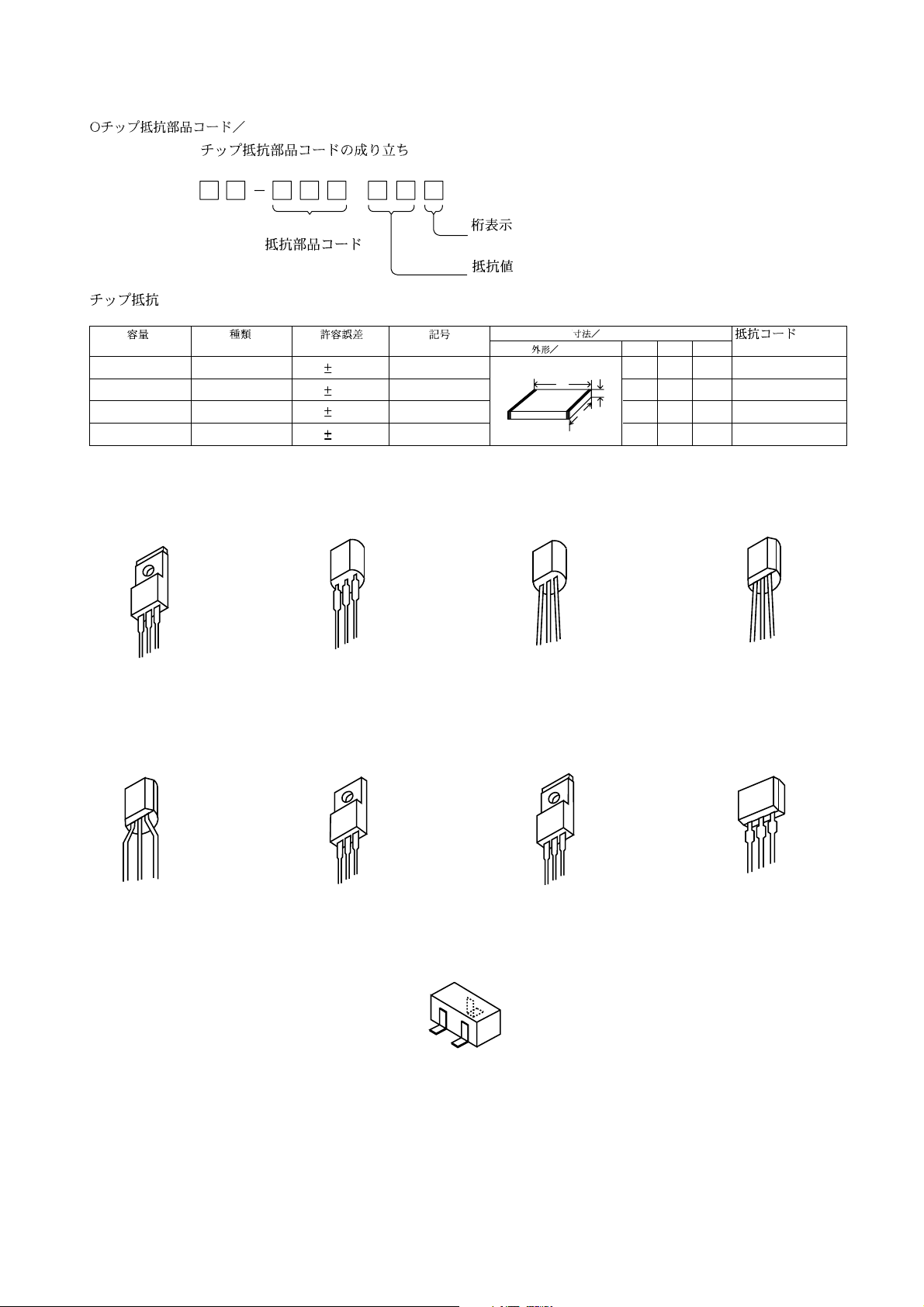
ELECTRICAL PARTS LIST - 16/16
• Regarding connectors, they are not stocked as they are not the initial order items.
The connectors are available after they are supplied from connector manufacturers upon the order is received.
CHIP RESISTOR PART CODE
Chip Resistor Part Coding
88
A
Resistor Code
Chip resistor
Wattage Type Tolerance
1/16W 1005 5% CJ
1/16W
1/10W
1/8W
1608
2125
3216
TRANSISTOR ILLUSTRATION -1/1
B C E
2SB1342
2SD1933
2SA1296GR
5%
5%
5%
E C B
Symbol
CJ
CJ
CJ
Figure
Value of resistor
Form
L
E C B
2SA1980G
2SA1981Y
2SC3331(T/U)
KTA1266GR
Dimensions (mm)
t
W
0.55
Resistor Code
108
118
128
E C B
LW t
1.0 0.5 0.35 104
1.6 0.8 0.45
2 1.25 0.45
3.2
1.6
2SC5343GL
: A
: A
E C B
2N5551C
B C E
2SB1548
2SA1235F
2SC3052F
2SD1306NE07TL
DTA114YKA
DTA124XKA
DTC114EKA
DTC114TKA
DTC114YKA
G D S
2SK2937
S D G
2SJ460
2SK2541
C
B
E
DTC124EKA
DTC124XKA
DTC144EKA
KRA102S
RT1N141C
SBT5401
SBT5551
SRA2202S
-21-
Page 22
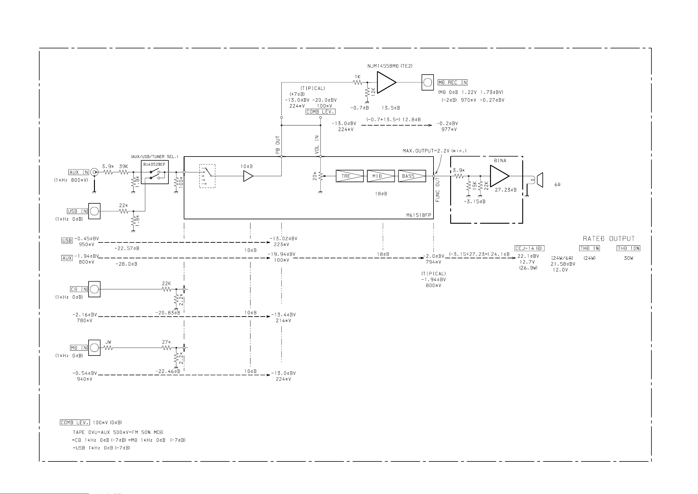
BLOCK DIAGRAM - 1/1 (LEVEL SECTION)
IC101
3,
MAIN C.B
IC602
1,
12
2,
15
31,
3,
32
13
5,
6
7,
8
5
1,
7
25,
26
IC601
J203
SPEAKERS
AMP C.B
29,
30
27,
28
-22-
Page 23
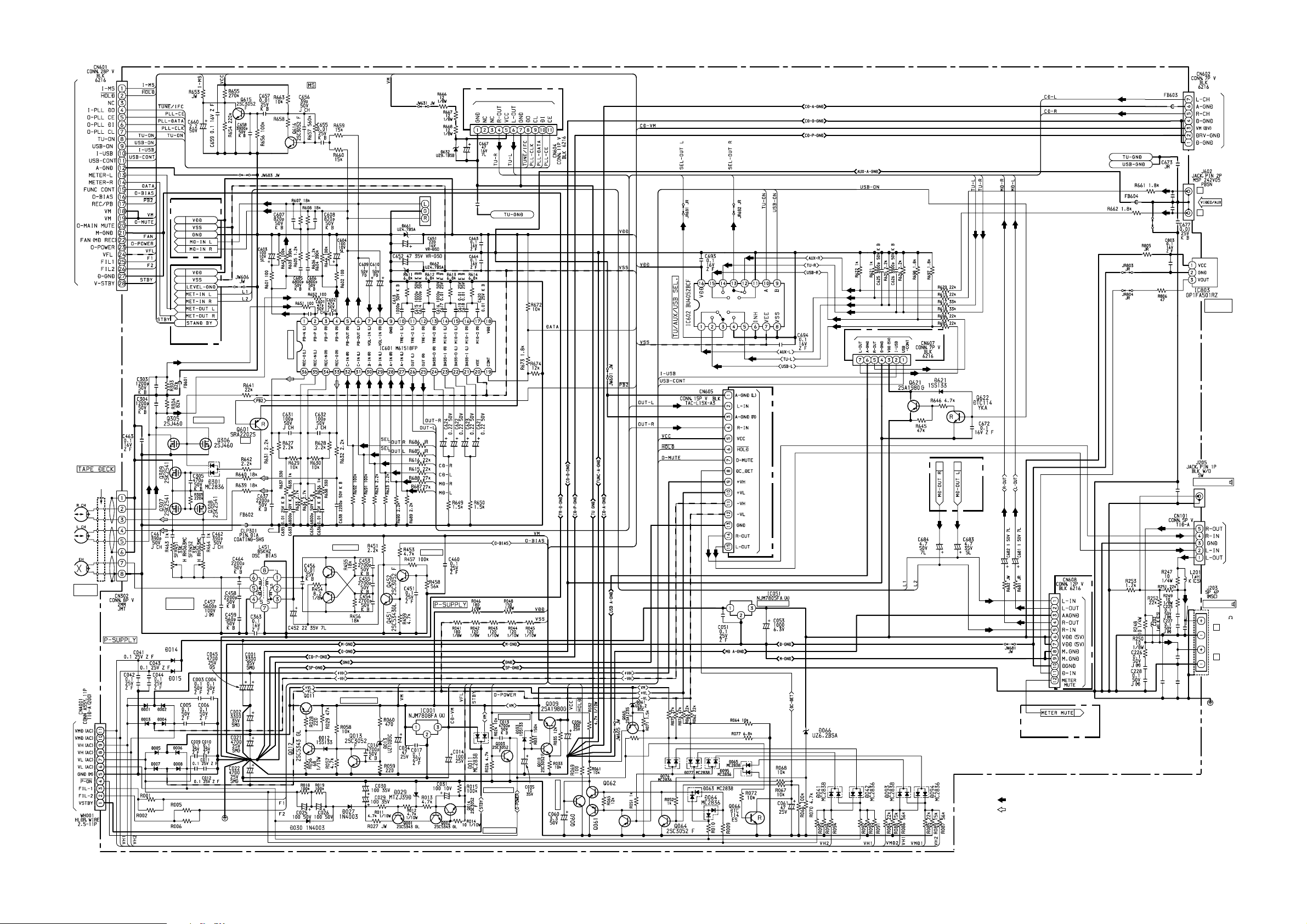
SCHEMATIC DIAGRAM - 1/10 (MAIN -1/3 SECTION)
TO MICON C.B CN111 VIA FFC601
TO MAIN C.B 2/3
(MD AMP SECTION)
3A-7A
3A
4A
5A
6A
7A
2B
3B
4B
5B
6B
7B
8B
9B
TO MAIN C.B 3/3
(LEVEL METER
SECTION) 2B-9B
JR
JR
IC601
FUNCTION
TP9
GND
TP8
TO TUNER PACK VIA FFC604
C676
0.1 16V ZF
MAIN C.B 1/3
TO USB C.B CN701 VIA FFC607
JW
TO CD C.B CN602 VIA FFC602
C669
560P
50V KB
JR
C670
560P
50V KB
W011
L
R
DIGITAL IN
(OPTICAL)
HEAD C.B
RPH
CNA302
AZIMUTH
ADJ.
RL203GW
D001-008
RL203GW x8
D
GG
S
D
S
S
G
D
SFR451,452
REC/PB
FREQ.ADJ.
RL203GW
G
Q305-309
REC/PB SW
S
G
D
D
SW
S
2A
1A
SUB WOOFER
C233
C231
0.01
25V KB
0.01
25V KB
C230
25V KB
0.015
C232
0.01
50V ZF
C229
0.015
SPEAKERS
50V ZF
SPEAKER
IMP:6
L
R
VIA CNA201
TO HP C.B WH101
TO AMP C.B CN601
JR
Q453
2SC3331T/U
2SC3331T/U
2SB1548
Q454
Q453,454
BIAS OSC
Q011-013,IC001
VOLTAGE REG.
Q451,452
BIAS SW
Q009,010
VOLTAGE REG.
R078
82K
VOLTAGE REG.
1A,2A
TO MAIN C.B 2/3
(MD AMP SECTION)
TO MAIN C.B 3/3
(LEVEL METER SECTION)
1B
1B
TO MICON C.B CN115 VIA FFC115
TO PT C.B CN081
VMD1
VMD2
1.5 1/4W
1.5 1/4W
1.5 1/4W
1.5 1/4W
W010
TO CHASSIS
Q003
RELAY DRIVE
Q001,002,014
VOLTAGE REG.
Q060-064
AC & DC DET
2SC3052F
2SC3052F
Q063
2SA1235F
2SA1235F
-23-
18K
18K
39K
18K
56K
39K
18K
:AUDIO (PB) SIGNAL
:AUDIO (REC) SIGNAL
56K
Page 24
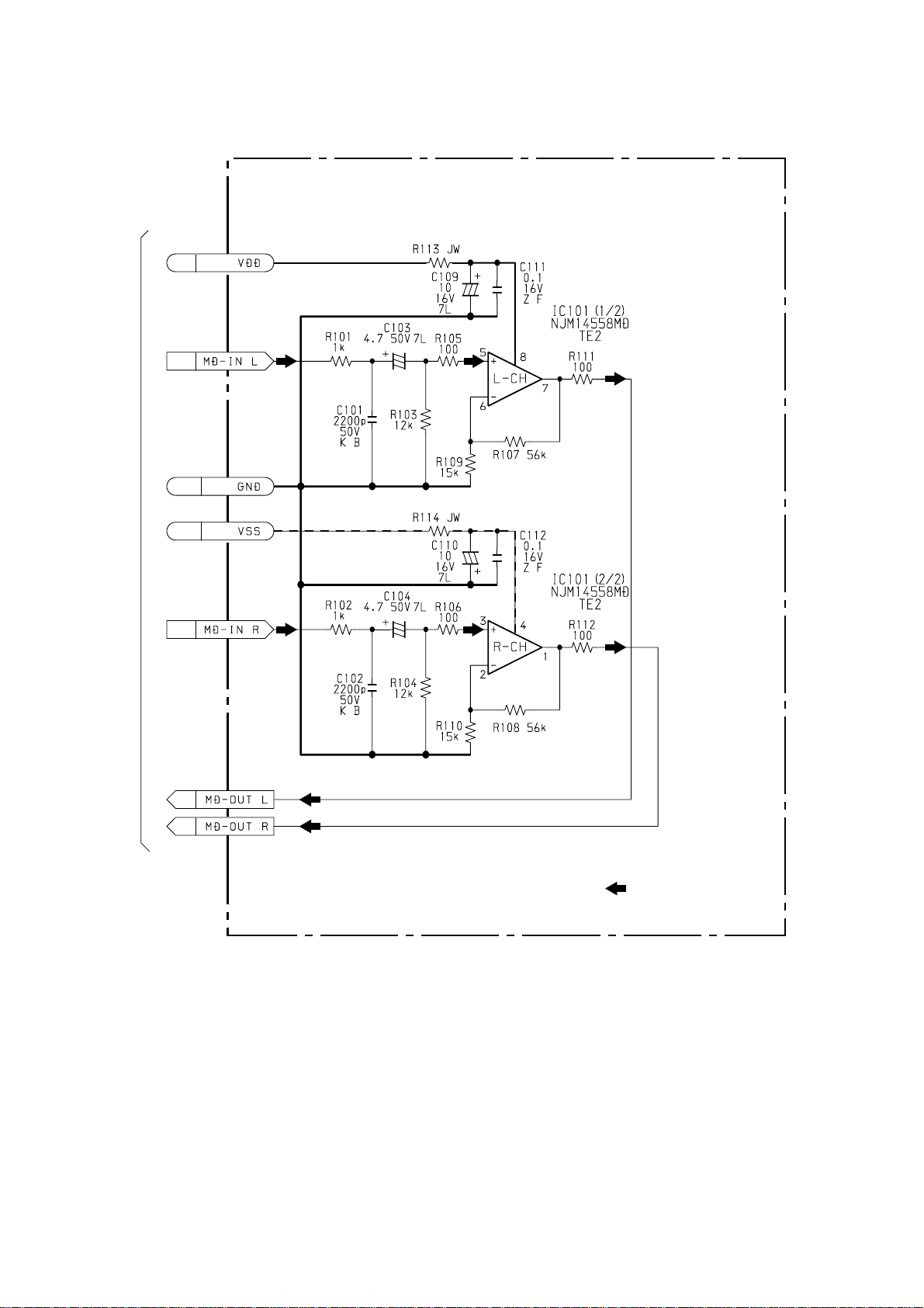
SCHEMATIC DIAGRAM -2/10 (MAIN-2/3 MD AMP SECTION)
MAIN C.B 2/3 (MD AMP SECTION)
3A
6A
5A
-
4A
TO MAIN C.B 1/3 1A-7A
7A
1A
2A
-
:AUDIO (PB) SIGNAL
-24-
Page 25
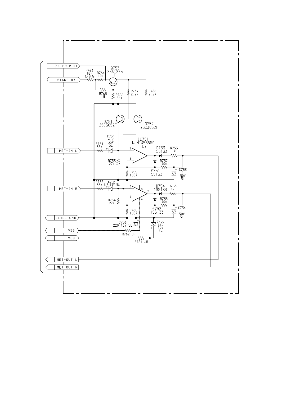
SCHEMATIC DIAGRAM -3/10 (MAIN-3/3 LEVEL METER SECTION)
MAIN C.B 3/3 (LEVEL METER SECTION)
1B
9B
5B
TO MAIN C.B 1/3 1B-9B
6B
4B
3B
2B
7B
8B
-25-
Page 26
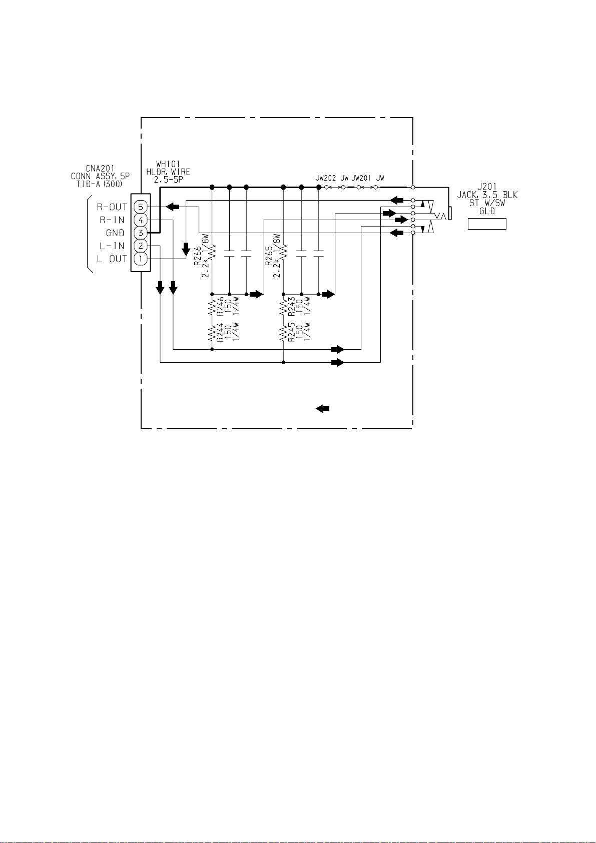
SCHEMATIC DIAGRAM -4/10 (HP SECTION)
HP C.B
TO MAIN C.B 1/3 CN101
680P 50V K B
C231
2200P 50V J CH
C224
C230
2200P 50V J CH
C223
PHONES
680P 50V K B
:AUDIO (PB) SIGNAL
-26-
Page 27
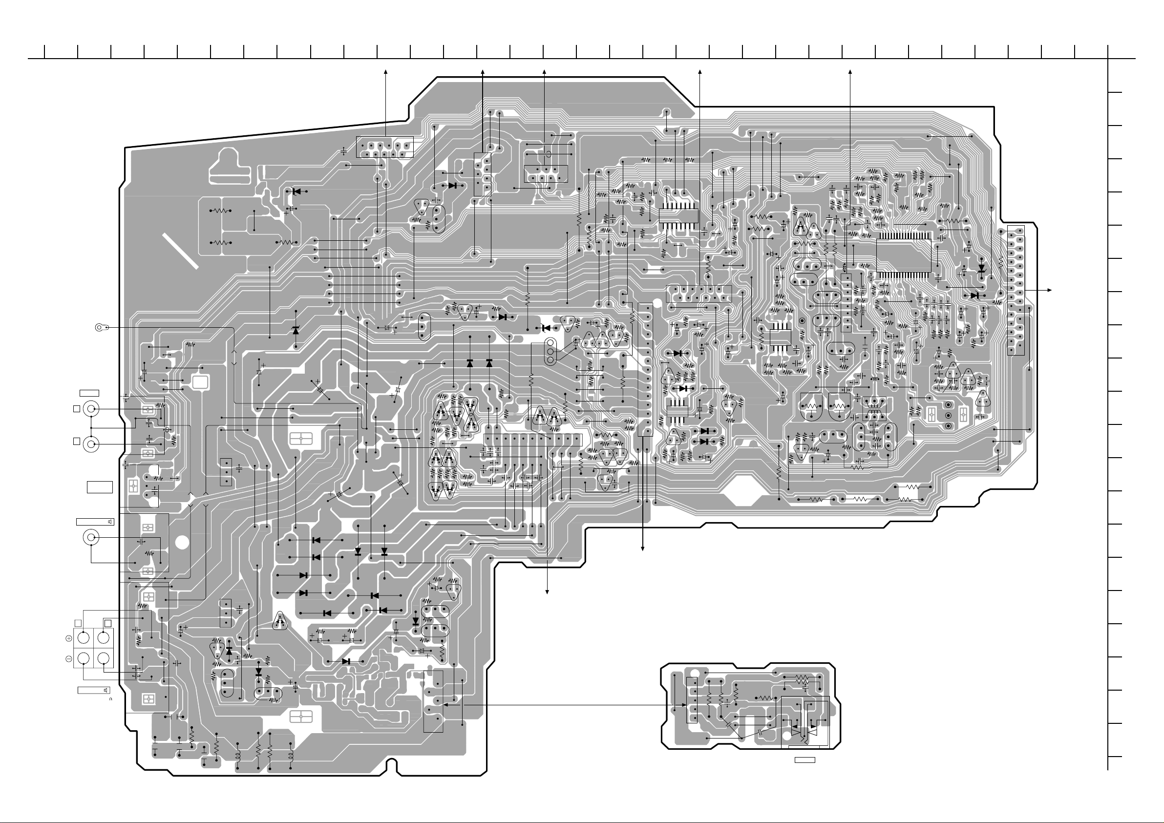
WIRING - 1/8 (MAIN C.B/HP C.B)
TO TUNER PACK
TO USB C.B CN701
TO CD C.B CN602
TO MICON C.B CN115
101112131415161718192021222324
TO HEAD C.B CNA302
1234567892526272829303132
A
TO CHASSIS
J602
AUX IN
R
L
IC803
DIGITAL IN
(OPTICAL)
J205
SUB WOOFER
R
J203
SPEAKERS
SPEAKER IMP:6
FFC604
FFC607
FFC602
MAIN C.B
1
2
C676
D632
CEB
R247
R058
R029
R056
D011
R248
C667
R668
D004
D003
L202
D066
C034
D002
D001
R019
C026
C001
C021
D007
D006
D005
R018
C025
D027
R666
R667
W010
R805
JR803
C053
J602
C673
C677
C233
R251
L
C229
R252
C231
C232
IC803
3
1
J205
C670
C669
R253
J203
R806
C803
C226
R662
JR804
C228
FB604
C230
R661
BLK
W011
C014
Q013
R057
R028
R250
C227
BLK
W012
R039
EB
C
C225
IC051
1
3
IC001
1
3
Q011
R249
BLK
C045
C051
C017
D013
R060
C016
B
D012
C
E
Q012
L201
CN604
C036
D030
C030
C022
D008
10
Q622
R646
JR002
C002
11
D029
C029
EB
C
R645
Q009
D093
R088
R096
R093
D041
R010
R013
B
C
E
R011
4
2
C672
Q621
R009
D063
R015
C031
CEB
R012
CEB
CN101
B
C
E
R089
R087
5
1
R033
D094
D064
R014
EB
R027
D621
R085
R086
C
Q002
Q001
EB
R035
Q010
JR005
D042
R092
R095
Q014
C
R084
R091
D065
JR006
C042
R094
2
6
D014
D077
C035
C004
C041
C006
1
7
C003
CN607
D033
D015
R070
C044
R031
R064
C043
WH001
C005
C009
FB603
CN602
R046
D061
B
C
E
Q066
R072
D095
C012
C011
C010
CNA001
TO PT C.B CN081
26
17
Q065
EB
C
D076
R078
JR007
CNA201
R048
R076
111
R071
C061
R075
R617
C060
Q061
C
BE
R051
R077
Q003
R066
R065
R068
Q063
R618
BE
Q062
R625
C
R052
EB
EB
C
R696
C
R698
C626
R620
C625
R619
R695
R061
R042
R032
EB
C
Q060
R069
R041
R063
R062
R067
Q064
EB
C
R026
C013
TO AMP C.B CN601
R043
R626
R621
CN605
R024
1
15
R044
C693
16 9
R622
1
JR705
Q751
R767
R752
Q752
R768
C
BE
FFC115
R045
IC602
8
JR692
R697
CN608
R751
C751
D753
R753
R759
D751
41
IC751
58
C
BE
R760
C752
R754
R758
C694
C753
R762
C756
R755
R757
D754
C755
D752
C754
JR691
R682
C683
R761
212
R764
EB
R756
C682
111
C
C681
Q753
R766
HP C.B
WH101
5
R245
R243
C223
1
C230
R681
R765
R265
R113
R114
R108
R107
C111
R266
C110
C103
R103
R105
R112
C231
C101
R111
C109
Q305
R109
CLP301
85
IC101
14
R110
R106
C684
SFR452
R763
J201
R641
D301
C112
R104
EB
Q452
R453
PHONES
R642
R101
Q306
DSG
C102
R459
C
J201
Q601
BE
DSG
R102
R458
R457
R244
C
R005
C224
C637
C104
C451
Q307
Q308
C462
R464
R246
R633
JR301
DSG
DSG
C461
C305
R463
C464
SFR451
Q451
C633
R639
CEB
R635
R305
C452
C638
R640
FB601
CN302
DGS
C458
R451
R637
1
8
C635
R627
R632
Q309
R454
R686
R638
C459
C363
B
C
E
Q454
R006
R685
R304
R303
R691
R692
C636
C634
R636
R634
R630
R629
R628
C632
C631
R631
36 19
R652
1
C601
C602
C304
R602
R601
R651
R644
C604
R643
C303
C463
C457
R603
C605
R605
FB602
L451
46
3
1
C460
B
C456
C455
C
R456
E
C454
R455
C453
R616
R624
C603
C607
R607
IC601
R604
C606
R606
Q453
R002
R623
C608
R608
R001
R660
R615
R689
C610
R688
R690
18
C615
R611
C609
R655
C659
R663
C657
R659
C614
C613
R612
R687
C617
C660
C658
R674
C616
C664
C663
C619
R613
R673
C620
618
R614
C
BE
R656
TP8(Rch)
GND
TP9(Lch)
R654
Q615
C651
C622
C624
BE
Q617
C
R658
C652
R650
D662
R649
R657
BE
D661
C
C621
C623
C655
R672
C656
Q616
R653
CN601
FFC601
TO MICON C.B CN111
B
C
D
E
F
G
H
I
J
K
L
M
N
O
P
Q
R
S
T
U
-27-
Page 28
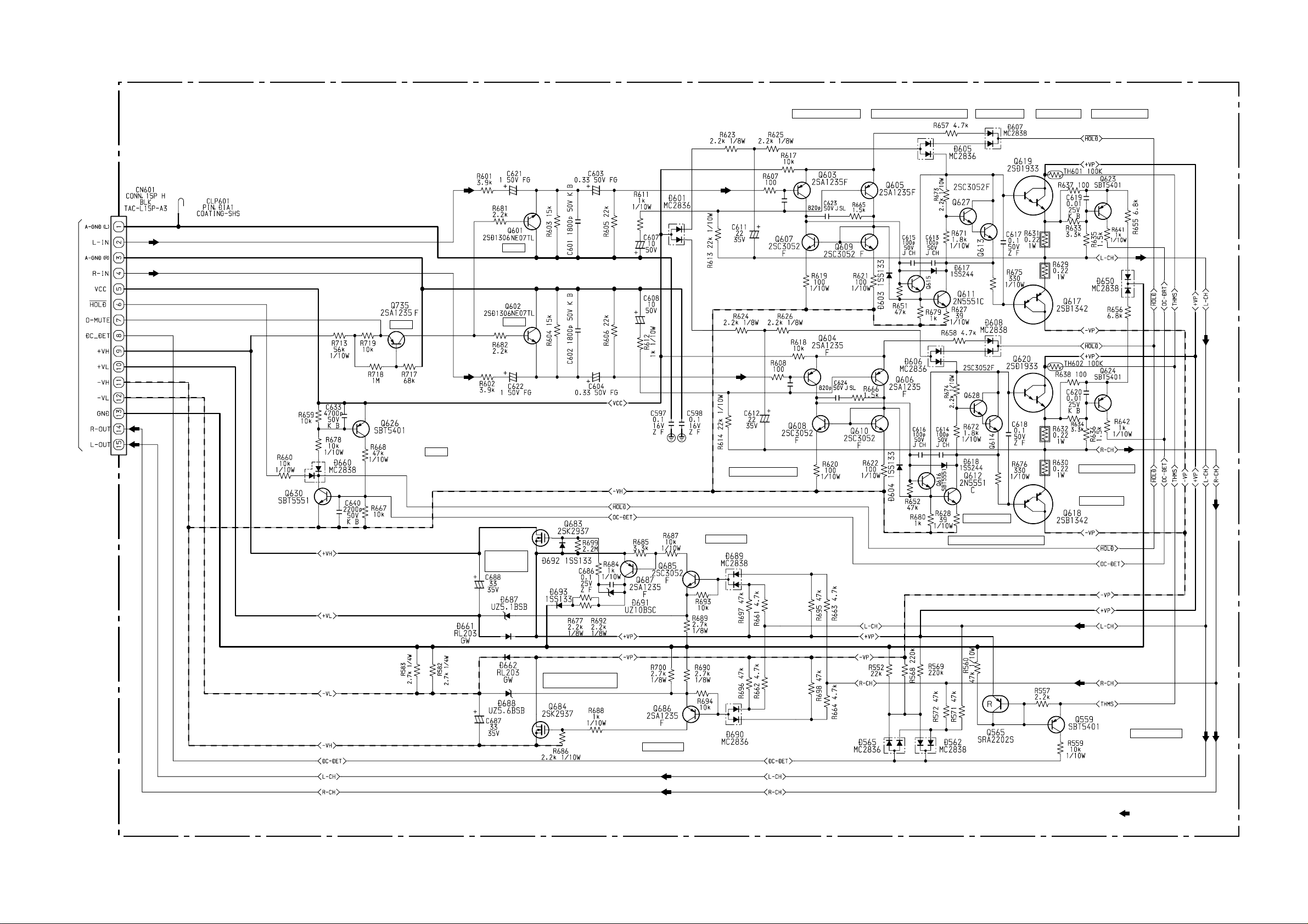
SCHEMATIC DIAGRAM - 5/10 (AMP SECTION)
TO MAIN C.B 1/3 CN605
AMP C.B
MUTE
MUTE
MUTE
C609
100P
50V J CH
50V J CH
C610
100P
Q603,605,607,609
DIFFERENTIAL AMP
CURRENT TO VOLTAGE AMP
Q611,615
Q615
SBT5551
Q613,627
Q614,628
Q613,627
BIAS CIRCUIT
Q617,619
POWER AMP
Q623
OVERLOAD DET
Q626,630
HOLD
Q683
+VH/+VL
SWITCHING
CIRCUIT
D
G
S
+VH/+VL
SWITCHING CIRCUIT
D
G
S
Q684
Q686
DETECTOR
Q604,606,608,610
DIFFERENTIAL AMP
Q685,687
DETECTOR
Q614,628
BIAS CIRCUIT
Q612,616
CURRENT TO VOLTAGE AMP
Q624
OVERLOAD DET
Q618,620
POWER AMP
Q559,565
THERMAL DET
-28-
:AUDIO (PB) SIGNAL
Page 29
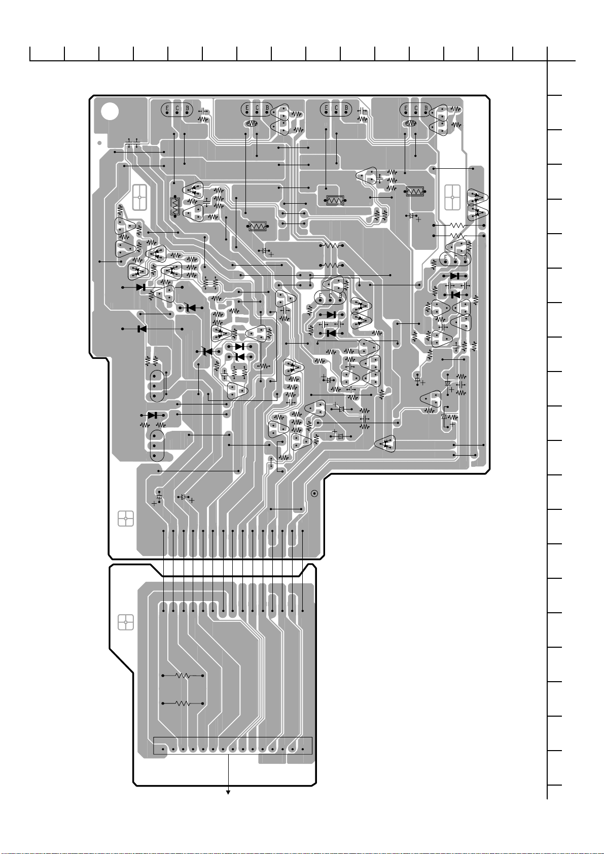
WIRING - 2/8 (AMP C.B)
123456789101112131415
AMP C.B
Q618
C597
C598
D650
R656
C
C
R568
R688
R559
D661
Q684
Q683
R569
R698
D692
R630
R552
C
R686
G
D
S
G
D
S
R696
D562
E
B
R684
R571
R694
C
Q624
R572
D690
R664
Q686
D688
D687
R560
Q559
R557
Q565
D565
D662
B
E
B
E
R699
E
B
R690
R662
R695
D689
R697
R685
C618
R676
R624
R661
R638
C620
R634
R636
R700
R687
Q620
TH602
C686
B
E
R663
R677
C
D693
D691
C
R632
R692
Q687
C612
E
B
R668
Q626
JR601
Q630
R689
Q685
Q628
E
C
B
E
C
B
Q614
R693
C633
B
E
B
E
C640
R667
C
R672
C
R717
R713
D660
R660
R659
B
E
R674
R678
R718
R719
Q735
C614
R680
C
C
Q616
R628
R614
C608
R682
R612
E
B
R624
C
D604
R620
Q602
R602
Q617
R629
R666
C624
Q608
E
B
C622
R626
C604
Q623
Q612
D618
R622
R652
C616
B
E
A
C617
R675
Q619
TH601
Q627
E
C
B
E
C
B
Q613
R671
R673
B
C
R637
E
C619
C
B
B
E
C
C
C
C610
R608
R604
D606
D608
R658
C
E
B
E
B
R618
R606
C602
R655
Q610
Q606
Q604
R635
R641
R633
D601
C611
R613
C607
R681
R621
R665
Q601
C
R631
C623
R619
R611
R625
R623
Q615
R627
C613
R679
Q607
E
B
D617
Q609
B
C
E
B
E
C
C
C603
D607
D605
C
C609
C621
E
B
C
D603
E
B
E
B
R601
C615
R607
R605
C601
R603
R651
Q611
Q605
Q603
R657
R617
D
E
F
G
H
I
J
K
L
C687
C688
R583
R582
CN601
CLP601
115
M
N
O
P
Q
R
S
T
U
TO MAIN C.B 1/3 CN605
-29-
Page 30
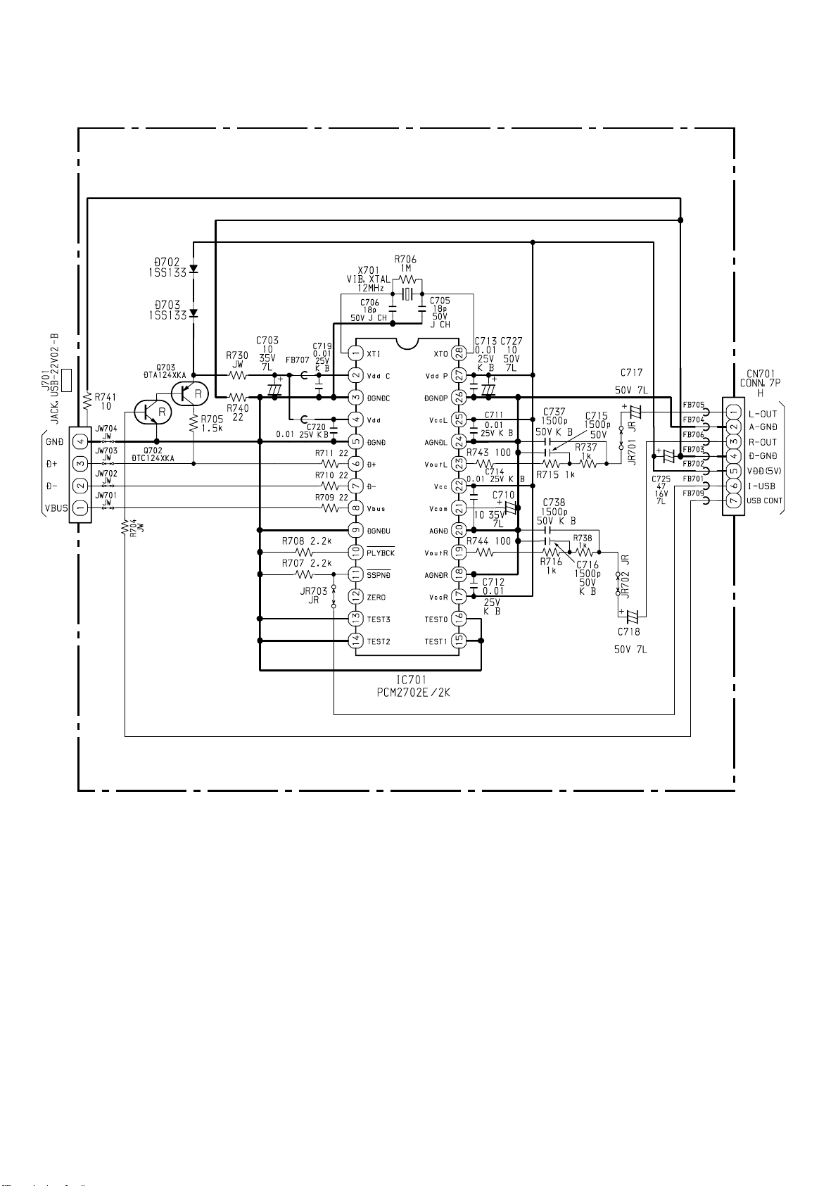
SCHEMATIC DIAGRAM -6/10 (USB SECTION)
USB C.B
USB
JR
FB708
JR
1
JR
JR
JR
JR
JR
JR
JR
TO MAIN C.B 1/3 CN607 VIA FFC607
1
USB DAC
-30-
Page 31

WIRING - 3/8 (USB C.B)
123456789101112131415
A
B
C
USB C.B
FB702
FB701
FB709
7
FFC607
1
TO MAIN C.B 1/3 CN607
CN701
FB706
C718
6
2
C725
FB703
FB704
FB705
D703
R704
D702
Q702
C717
JR701
C738
Q703
EB
C
C
BE
R740
C737
R745
R721
C716
R738
JR702
C715
R737
R716
R730
R705
C703
R708
R707
R715
R743
R744
JR703
R711
R709
R710
14 1
IC701
15 28
C712
JR709
C711
C710
C714
2
1
FB708
C720
C719
R741
J701
3
4
FB707
C706
C705
JR710
X701
C727
C713
R706
J701
USB
D
E
F
G
H
I
J
K
L
M
N
O
P
-31-
Q
R
S
T
U
Page 32

SCHEMATIC DIAGRAM - 7/10 (MICON/DECK SECTION)
TO MAIN C.B 1/3 CN601 VIA FFC601TO CD C.B CN601 VIA FFC110
MICON C.B
TP1
(CLK)
TO KEY C.B CN108 VIA FFC114TO METER C.B CN109 VIA FFC112
JW131 4.7K
PIN2
(GND)
TO MAIN C.B 1/3 CN608 VIA FFC115
C806
8.2P
JW
R137
15P
C152 33P 50V J CH
IC102
LC8752B2A-50Y2
15P
12P
C153 33P 50V J CH
C805
8.2P
DECK C.B
FFC116
CN1
SOL1
C803
SW1
(RECB)
8.2P
(STOP)
C804
8.2P
32
1
SW2
IC1
DN6851
TO CD C.B CN603 TO MD ASSY VIA FFC117
SW3
(CST)
JR
SW4
(RECA)
M1
(DECK MOTOR)
CRD1
-32-
Page 33

SCHEMATIC DIAGRAM - 8/10 (KEY/METER/LED SECTION)
KEY C.B
10P
10P
10P
10P
JW
(DISPLAY)
D
D
D
D
METER C.B
(LEVEL METER)
TO MICON C.B CN114 VIA FFC114
STANDBY/ON
MULTI JOG
IC103
(REMOTO SENSOR)
C122
100P 50V J CH
S101
POWER
STANDBY/ON
KSHG611BT
S103
ECO
KSHG611BT
VOLUME
S105
TUNING
+
KSHG611BT
PUSH ENTER /DEMO
GROUP / PRESET
VOLUME
KSHG611BT
KSHG611BT
KSHG611BT
KSHG611BT
KSHG611BT
KSHG611BT
KSHG611BT
-
S109
S111
/
S107
/
TUNING
SP/LP
CLEAR
S114
REC SEL /
REC MUTING
S116
REC SEL
CD SYNC /
S118
REC PAUSE
REC START/
S120
CD MD
REC x4
LED C.B
D105,106
(LEVEL METER
LIGHTING)
TO MICON C.B CN112 VIA FFC112
S102
KSHG611BT
CD
KSHG611BT
S104MDS106
KSHG611BT
/BAND
TUNER
S108
KSHG611BT
TAPE
S110
KSHG611BT
D-IN
AUX /
KSHG611BT
S112
JOG MODE
S115
KSHG611BT
EDIT
KSHG611BT
S117MDS119
KSHG611BT
CD
-33-
Page 34

WIRING - 4/8 (MICON C.B/KEY C.B/METER C.B/LED C.B)
METER C.B
Q114
R188
JR105
LM101
R282
LED102
S113
BE
R150
R145
Q113
S123
MULTI JOG
GROUP/PRESET
EB
R187
CEBC
R198
Q106 Q104
R281
FFC114
R212
R136
R170 CN108
1
C
2
(DISPLAY)
S102
CD
S104
MD
S106
TUNER
/BAND
S108
TAPE
S110
AUX/
D-IN
S112
JOG MODE
S115
EDIT
S117
MD
S119
CD
JR101
JR102
CN109
8
7
2
1
R283
R284
LM101 (LEVEL METER)
FFC112
S102
KEY C.B
S113,LED102
VOLUME
C120
3
1
C117
R158
R157
R159
R146
S123
C122
R151
2
1
R160
C118
C121
PUSH ENTER/DEMO
S112
S117
S119
R213
S104
R214
S106
R215
S108
R216
S110
R217
4
53
R218
S115
R221
R219
R220
R186
17
16
FL101
FL101
R269
R275
Q115
(REMOTE SENSOR)
R280
R274
R279
Q116
C145
C148
C147
C146
R273
R272
R278
R277
BE
IC103
C115
R271
C
R110
LED C.B
1
R276
5
CN105
R102
R101
C114
R147
R138
34
15
IC103
C102
C101
R105
R106
C103
4935 451
C105
C106
C104
R108
Q111
C
BE
D110
R227
R233
CN106
5
1
S109
S105
R174
S111
S114
S116
R178
S118
R179
S120
R229
R228
C136
R226
R222
LED101
S101
S103
R173
S107
D106
C138
R224
D105
C131
C130
R223
(LEVEL METER LIGHTING)
R148
S101,LED101
POWER
STANDBY/ON
R171
S103
ECO
R172
S109
CLEAR
S105
/
TUNING
S107
/
R175
S111
SP/LP
S114
REC SEL/
REC MUTING
R176
R177
S116
CD SYNC/
REC SEL
S118
REC START/
REC PAUSE
S120
CD MD
REC x4
D105,106
+
FFC112
FFC114
FFC601
TO MAIN C.B 1/3 CN601
R126
R129
R131
R231
CN112
2
8
CN114
17
1
JW131
101112131415161718192021222324
MICON C.B
TO DECK C.B CN1 TO CD C.B CN603
C201
1
7
16
CN111
JW161
2
2
28
27
R232
C137
1
CN116
8
7
Q109
R238
Q103
R120
R118
R124
R133
R117
R116
R132
FFC116
R162
EB
C
R141
R114
R130
2
1
D109
Q110
R251
R237
C
Q108
R122
R149
R161
EB
C116
C
R243
R115
R127
R113
R112
1
2
R181
TO CD C.B CN601
R250
EB
R242
D103
Q101
R169
R183
R185
R267
CN110
R247
R245
C
R235
R144
Q102
R137
FFC110
CLP101
Q112
EB
R121
R197
R199
R239
R119
80
R135
81
R200
13
12
R268
D101
C113
R201
R234
R168
C112
R203
R111
PIN2
(GND)
TP1
(CLK)
R202
R189
R163
R128
100
R123
C108
D102
51
IC102
C128
R166
R154
R180
R125
1
X101
C139
R182
R190
R191
C129
15
CNA101
14
C802
C143
Q105
50
JR106
C152
C140
R209
R244
R246
EB
C
R143
R140
C119
C127
JR107
R225
46
3
L102
1
C142
R164
31
30
C141
1
IC802
Q107
C
BE
D107
JW149
R195
R194
C135
C153
8
7
R241
R236
JW150
R208
C804
C803
C805
C801
R152
R155
R802
R801
R196
R207
R803
R153
R165
JR807
IC801
1147
R156
R192
R193
R206
R205
R204
JR806
C809
8
C810
54
IC804
13
C806
CN117
28
27
R210
R211
2
1
JR801
C811
JR802
R252
12 2
CN115
FFC115
TO MAIN C.B 1/3 CN608
C808
R808
C812
JR803
FB801
R809
JR804
FFC117
1234567892526272829303132
A
B
C
D
E
F
G
H
I
J
K
L
M
TO MD ASSY
N
O
P
111
Q
R
S
T
U
-34-
Page 35

WIRING -5/8 (DECK C.B/HEAD C.B)
123456789101112131415
A
DECK C.B
RPH/EH
TO MICON C.B CN116
FFC116
19
28
CRD1
B
C
D
E
F
G
H
I
J
HEAD C.B
WHT
RED
RED
WHT
BLK
WHT
GRY
BLK
WHT
BLK
CNA302
TO MAIN C.B CN302
BRN
WHT
RED
BLK
RED
WHT
18
BLK
K
L
M
N
O
P
Q
R
S
T
-35-
U
Page 36

SCHEMATIC DIAGRAM - 9/10 (CD SECTION)
12K
CD C.B
1K
470P
4.7M
0.22
33K
330
C698
0.1
22
C699
0.1
VOUT-R
VOUT-L
VCOM
C696
3.3P
C697
3.3P
C695
3.3P
WHT
470P
1200P
2700P
3.3K
22P
50V J CH
15P
FFC501
SW2
FFC503
CON3
SW3
(CLOSE)
FFC502
CON2
M1
SW1
M2
M3
MOTOR
LOADING
(OPEN)
CD DRIVE C.B CD TRAY C.B
2SA1981Y
F-BEAD
BL02RN2
100
100
100
100
FB601FB602
F-BEAD
BL02RN2
C694
0.1
W602
TO CHASSIS
TO MAIN C.B 1/3 CN602 VIA FFC602 TO MICON C.B CNA101TO MICON C.B CN110 VIA FFC110
-36-
Page 37

WIRING - 6/8 (CD C.B)
101112131415161718192021222324
1234567892526272829303132
CD C.B
FFC110
TO MICON C.B CN110
CN601
13
1
TO CHASSIS
12
C685
C684
2
C681
W602
C683
C682
R689
C694
C514
R520
R504
C506
R602
C513
C515
C603
R634
EB
C
C625
C504
C503
C519
C520
R629
X602
R631
R501
C699
1
RF
R624
C619
C698
2
C501
EB
C
C618
TO PICK UP ASSY
FFC501
R503
JR601
Q601
15
C614
16
JR602
TE
FE
VC
R616
C601
C602
R613
R601
R610
C609
R557
IC602
R695
BCE
C554
C
BE
R551
R660
C551
R656
2
6
R693
FB602
1
5
CN602
2
6
FB601
A
B
C
D
E
F
FFC502
TO CD MECHANISM
G
H
I
1
J
FFC602
K
7
TO MAIN C.B 1/3 CN602
L
M
N
O
FFC503
TO CD MECHANISM
C606
R653
C627
5
4
2
1
C672
C673
R603
R633
R635
R639
R636
C605
R637
R604
Q602
R659
C651
R657C655
C652
R655
C695 C697
1
5
TO MICON C.B CNA101
C653
C696
P
Q
R
S
T
U
-37-
Page 38

WIRING - 7/8 (CD DRIVE C.B/CD TRAY C.B)
123456789101112131415
A
TO CD C.B CN502
CD DRIVE C.B
M2
FFC502
M2
B
C
CON2
D
E
F
G
H
I
J
CD TRAY C.B
SW3
SW2
SW3
SW2
CON3
M1
K
L
M1
M
N
O
M3
P
Q
R
S
FFC503
TO CD C.B CN503
T
U
-38-
Page 39

SCHEMATIC DIAGRAM -10/10 (PT SECTION)
PT C.B
PT,K CCJ-E
TO MAIN C.B 1/3 WH001 VIA CNA001
PT,SUB BMA E (VRK)
AC230V,50Hz
-39-
Page 40

WIRING - 8/8 (PT C.B)
TO MAIN C.B 1/3 WH001
CNA001
PT C.B
123456789101112131415
A
B
C
CN081
C081
JW088
PR082
JW086
D081
C086
D085
D083
D082
D084
RY081
PR081
AC230V,50Hz
C087
PT081
4
8
CN082
2
6
1
1
102
111
JW087
JW085
D
E
F
G
H
I
J
K
L
17
C085
W081
TO SHASSIS
1
M
N
O
P
Q
7
8
R
S
T
U
-40-
Page 41

ELECTRICAL ADJUSTMENT -1/5
<DECK Section>
MAIN C.B (PATTERN SIDE)
SFR452
SFR451
TP8
TP9
6
R
G
L
1
2
3
4
5
6
7
DECK MOTOR
1
MOTOR SFR
3
RPH
FWDRVS
-41-
Page 42

ELECTRICAL ADJUSTMENT -2/5
TP8,TP9
<DECK SECTION>
Make the following preparations for DECK adjustment.
Preparations
• Measuring instruments: Audio signal oscillator/Attenuator/Wow-Flutter meter (frequency counter)/Oscilloscope/Millivoltmeter/Dummy
resistance (6Ω)
• Test Tape: TTA-100 / TTA-330/ TTA-200 / TTA-602 (or equivalent test tape for play/record)
1. Tape Speed Adjustment and Check
Requirements
* Measuring instruments: Wow-flutter meter (frequency counter)
Test tape: TTA-100 (3 kHz)
Test point: TP8 (Rch), TP9 (Lch)
Adjustment point: MOTOR SFR
(1) Connect the TP8 and TP9 of the unit to the wow-flutter meter.
(2) Insert the test tape (TTA-100) to DECK. Playback the middle part of the tape in the FWD
direction, and adjust MOTOR SFR so that the level, 3,000 Hz ± 5 Hz can be obtained.
(3) Playback RVS, and check that the speed is less than ± 45 Hz to the speed of FWD.
2. Wow-Flutter Check
* Measuring instruments: Wow-flutter meter (frequency counter)
Test tape: TTA-100 (3 kHz)
Test point: TP8 (Rch), TP9 (Lch)
(1) Connect the TP8 and TP9 of the unit to the wow-flutter meter.
(2) Switch the wow-flutter setting from INDICATOR to JIS, and from a mode to W RMS (WTD).
(3) Playback the middle part of the test tape (TTA-100), and check that the level is 0.25 % or below.
TP8,TP9
3. Head Azimuth Adjustment
Requirements
* Measuring instrument: Oscilloscope
Test tape: TTA-330
Test point: TP8 (Rch), TP9 (Lch)
Adjustment point: Head azimuth adjustment screw
(1) Connect the CH1 of the oscilloscope probe to TP9 (Lch) and the CH2 to TP8 (Rch).
(2) Set the V mode of the oscilloscope to ADD.
(3) Insert the test tape (TTA-330) to DECK 1. Playback the middle part of the tape in the
FWD direction, and adjust the head azimuth adjustment screw so that the waveform
reaches maximum when 8 kHz is played.
(4) Apply the above steps to the side of RVS.
(5) After adjustment, lock the screw by bonding (1620B).
4. Playback Frequency Check
Requirements
* Measuring instrument: Millivoltmeter
Test tape: TTA-330 (315 Hz / 8 kHz)
Test point: TP8 (Rch), TP9 (Lch)
(1) Connect the CH1 of millivoltmeter to TP9 (Lch) and the CH2 to TP8 (Rch).
(2) Insert the test tape (TTA-330) to DECK, and playback 315 Hz and 8 kHz.
(3) Check that the 8 kHz level is ranged within 0 ± 5 dB compared to the output reference
level of 315 Hz.
-42-
Page 43

ELECTRICAL ADJUSTMENT -3/5
5. Playback Sensitivity Check
Requirements
* Measuring instrument: Millivoltmeter
Test tape: TTA-200 (400 Hz)
Test point: TP8 (Rch), TP9 (Lch)
(1) Connect the CH1 of millivoltmeter to TP9 (Lch) and the CH2 to TP8 (Rch).
(2) Insert the test tape (TTA-200) to DECK to playback.
(3) Check that the output level is ranged within 145 mV ± 3 dB.
6. Playback/Record Frequency Response Adjustment
Requirements
* Measuring instruments: Millivoltmeter
Audio signal oscillator (low-frequency oscillator)
Attenuator
Test tape: TTA-602 (LH)
Test point: TP8 (Rch), TP9 (Lch)
Input point: AUX (1 kHz / 8 kHz)
Adjustment point: SFR451 (Lch), SFR452 (Rch)
(1) Connect the CH1 of millivoltmeter to TP9 (Lch) and the CH2 to TP8 (Rch).
(2) Connect the output terminal of oscillator to attenuator, and then attenuator to AUX of the unit.
(3) Insert the test tape (TTA-602) to DECK, and record the 1 kHz signal from AUX.
(4) Adjust the attenuator so that the output levels of TP8 and TP9 become 17 mV.
(5) Record 1 kHz and 8 kHz alternately.
(6) Adjust SFR451 (Lch) and SFR452 (Rch) so that the playback output level of 8 kHz is ranged within 0 ± 1 dB compared to the
playback output reference level of 1 kHz.
k
7. Playback/Record Sensitivity Check
Requirements
* Measuring instruments: Millivoltmeter
Audio signal oscillator (low-frequency oscillator)
Attenuator
Test tape: TTA-602 (LH)
Test point: TP8 (Rch), TP9 (Lch)
Input point: AUX (8 kHz)
(1) Insert the test tape (TTA-602) to DECK, and record the 8 kHz signal from AUX.
(2) Adjust the attenuator so that the output levels of TP8 and TP9 become 170 mV.
(3) Playback 8 kHz, and check that the output level is ranged within -1 dB ± 3.5 dB compared to the output level during recording.
-43-
Page 44

ELECTRICAL ADJUSTMENT -4/5
<FRONT Section>
MICON C.B (PARTS SIDE)
8
<FRONT SECTION>
L102
TP1
(CLK)
JW150
JW149
PIN2
(GND)
8. Clock Adjustment
Requirement
* Measuring instrument: Frequency counter
Test point: TP1 (CLK), PIN2 (GND)
Adjustment point: L102
(1) While pressing and holding down the POWER button and the TUNER button, insert the AC plug.
(2) Adjust L102 so that the frequency counter indicates 176.83 ± 1.59 Hz.
(3) Draw out the code, and short-circuit JW149 and JW150 for about 2 seconds.
-44-
Page 45

ELECTRICAL ADJUSTMENT -5/5
VOLT / DIV: 500mV
TIME / DIV: 0.2 s
EYE PATTERN
must be CLEAR and MAX
Approx.
1.8 0.3Vp.p
4
<CD AAdjustment>
• Adjust and check at test mode.
• Keep at a level CD Mechanism.
• Equipment
Measure: Oscilloscope (using probe 10:1)
Digital Multimeter (using at DCV range)
Jitter Meter (KIKUSUI 6235)
Test Disc: TCD-782/ATD-001
R515
IC501
1 2 1
RF
IC601
2
CD C.B (PATTERN SIDE)
VC
TE
FE
IC 505
1. RF Waveform Check
1) Connect the Oscilloscope to Test Point (RF+) and (GND).
2) Play second track of TCD-782.
3) Check that the amplitude of RF waveform is maximum, and that the lozenge
of center appear clearly.
2. Jitter Check
1) Keeping on connecting Oscilloscope to 2, connect the output pin of
Oscilloscope to the input pin of Jitter Meter.
2) Tune the knob of Oscilloscope voltage range at less than 500 mV.
3) Play second track of TCD-782.
4) Check that the display of Jitter Meter is as less than 28.0 nS.
3. Play Ability Check
1) Play track 3, 8, 13 of ATD-001, and check playing makes any noise or sound jump.
4. Lasor Current Check
* Don’t do this check except if the Lasor is fault.
1) Connect the Multimeter to both side of R504 (4.7Ω)
2) Play TCD-782, and check the DC voltage value of the Multimeter.
3) Check that the Lasor current (Iop = DC voltage value devided by R504 (4.7Ω))
is less than 80 mA.
RF
GND
RF
GND
OSCILLOSCOPE
OUTPUT
OSCILLOSCOPE
OUTPUT
JITTER METER
INPUT
DIGITAL MULTIMETER
ns
V
R504
R504
-45-
Page 46

CD TEST MODE -1/1
1. Starting CD Test Mode
While pressing and holding down the CD FUNCTION button, insert the AC plug to outlet.
When test mode starts, the message, CD TEST appears on the display, and all indicators light..
2. Exiting CD Test Mode
Press the POWER button or remove the AC plug from outlet.
3. Function of CD Test Mode
No Mode Function Key
1 Start Mode
2 Search Mode STOP button
34Play
5 Sled mode CD TEST PU moves to the innermost position.
Mode PLAY/PAUSE
Traverse Mode
Normal
button
PLAY/PAUSE
button
FF button
RWD button
Display
All indicators
light
READING
Normal
CD TEST
All FL indicators light
LD constantly light
Focus
Spindle motor continuous kick
Normal playback Each servo circuit check
If TOC READ is unavailable,
focus search is continued.
CLV error is ignored.
Tracking servo OFF/ON
Each time PAUSE button is pressed, the
tracking servo repeats turning OFF/ON.
At the same time, lens is kicked toward
outer position.
PU moves to the outermost position.
At the same time, lens is kicked toward
outer position.
Movement Check
search continuous
movement *1
FL check
Microcomputer check
APC circuit check
Laser current electricity measurement
Focus search waveform check
Focus error waveform check
RF waveform check
Tracking balance check
Sled circuit check
Tracking circuit check
Mechanism movement check
PU check
When Focus Search operates continuously more than 10 minutes, the protection circuit is activated due to heat generation of the driver IC.
* 1
In this case, turn off the power. After cooling down, restart the machine.
Be careful not to damage the gear because the sled motor rotates while the FF or RWD button is being pressed even if the pickup is located in
* 2
the innermost track or the outermost track.
-46-
Page 47

FL DISPLAY -1/1 <15-BT-89GINK>
GRID ASSIGNMENT ANODE CONNECTION
PIN CONNECTION
-47-
Page 48

IC BLOCK DIAGRAM -1/3
IC, M61518FP
PB-N(L)
PB-P(L)
PB-P(R)
PB-N(R)
PB-OUT(R)
PB-OUT(L)
VOL-IN(L)
VOL-IN(R)
REC-O(L)
REC-N(L)
REC-N(R)
REC-O(R)
C-IN(R)
C-IN(L)
B-IN(R)
B-IN(L)
A-IN(R)
A-IN(L)
GND
TRE-I(L)
TRE-O(L)
TRE-I(R)
TRE-O(R)
MID-I(L)
MID-O(L)
MID-I(R)
MID-O(R)
VDD
OUT(L)
OUT(R)
BASS-O(R)
BASS-I(R)
BASS-O(L)
BASS-I(L)
VEE
CONT
-48-
Page 49

IC BLOCK DIAGRAM -2/3
IC, PCM2702E/2K
D+
D-
V
BUS
DGNDU
VDDC
DGNDC
6
7
8
9
2
3
PLYBCK
USB
I/F
mclk
USB
Clock
Generator
Crystal
OSC
SSPND
USB
Packet
Data
wrclk
FIFO
SpAct
Audio
Data
rdclk
L
ZERO
121110 25 24 17 18
8x
Digital Filter
Multi-
Level
Delta-
Sigma
Modulator
CC
V
DAC
DAC
AGNDL
System Clock
Audio
Clock
Generator
Power Supply
5420222627281
VDDP DGNDPXTI XTO VCCAGND VDDDGND
R
CC
V
AGNDR
Low-Pass
Low-Pass
Filter
Filter
L
V
OUT
23
21
V
COM
19
V
R
OUT
IC, BA5813FM
BIAS
RVCC
REG-B
REG-P
RGND
TE-IN
FE-IN
MUTE2
PWVCC
GND
O-FE-
O-FE+
O-TE-
28 27 26 25 24 23 22 21 20 19 18 17 16 15
LOADING PRE
FWD REV
10K10K
LEVEL
SHIFT
LEVEL
SHIFT
10K
CH2-CH4
MUTE
POWVcc3,4
10K
10K
VBG
CH1
X3
MUTE
10K
7.5K
10K
16K
5K
PREVcc
21K
POWVcc1,2
(CH1,CH2)
(CH3,CH4)
10K10K
10K
10K
10K
10K
10K
LEVEL
SHIFT
LEVEL
SHIFT
1 2 3 4 5 6 7 8 9 10 11 12 13 14
O-TE+
10K
10K
10K
10K
OPEN
CLOSE
LDCONT
MUTE1
SL-IN
SP-IN
PRVCC
-49-
PWVCC
O-CL
O-OP
O-SP-
O-SP+
O-SL-
O-SL+
Page 50

IC BLOCK DIAGRAM -3/3
IC, PCM1742KE
BCK
LRCK
DATA
MLAT
MCLK
MD ATA
SCK
1
3
2
15
14
13
16
Audio
Serial
Port
Serial
Control
Port
System Clock
Manager
Oversampling
Digital Filter
System Clock
DAC
4x/8x
with
Function
Controller
12 11 6 9
ZEROL
Enhanced
Multilevel
Delta-Sigma
Modulator
DAC
Zero Detect
ZEROR
Output Amp and
Low-Pass Filter
Output Amp and
Low-Pass Filter
Power Supply
5 4
DD
V
DGND
V
CC
AGND
7
V
L
OUT
10
V
COM
V
OUT
R
8
IC, BU4052BCF IC, AN22002A
32
A
31
C
30
B
29
D
27
E
28
F
17
VREF
RFN
RFOUT
RFIN
CAGC
ARF
CBDO
BDO
COFTR
4 5 6 7 8 11 12 13 14
RF EQ
AMP
AMP
AMP
AMP
AGC
RFDET
GCA BCA
GCA BCA
GCA BCA
GCA BCA
BDO OFTR
3TENV
SUB
SUB
VDET
24 26 25 16 3
OFTR
9
10
15
22
23
21
20
19
18
2
1
CEA
3TOUT
RFDET
FEN
FEOUT
TEN
TEOUT
TEBPF
VDET
LD
PD
-50-
GCTL
TBAL
FBAL
GND
VCC
Page 51

IC DESCRIPTION -1/2 (LC8752B2A-50Y2) -1/3
Pin No. Pin Name I/O Description
1
O-CDT CLOSE
CD tray close output
O
10
11
12
13
14
15
16
17
18
19
20
2
3
4
5
6
7
8
9
O-CDT OPEN
O-CD-RESET
I-CD-BLKCK
I-CD-SENSE
________
O-CDX4
I-RMC
_______
I-RESET
XT1
XT2
VSS1
CF1
CF2
VDD1
_____________
O-CLK SHIFT
____________
I-HOLD(AD)
I-MS(AD)
I-KEY1(AD)
I-KEY2(AD)
I-ENC1(AD)
CD tray open output
O
CD reset output
O
CD sub-code clock input
I
CD sense input
I
Not used
–
Remote control sensor data input
I
Reset input signal
I
Crystal connect signal
I
Crystal connect signal
O
Ground
–
Input signal of LC oscillator
I
Output signal of LC oscillator
O
Power supply
–
Microcomputer clock shift switching
O
HOLD voltage input
I
Signal level input for TAPE music sensor
I
Input tact key 1
I
Input tact key 2
I
Volume control input
I
21
22
23
24
25
26
27
28
29
30
31
32
33
34
35
36
37
38
39
40
I-ENC2(AD)
I-DECK SW(AD)
O-MD-KDATA
I-MD-MDDATA
O-MD-DSCK
O-CD-MDATA
I-CD-STAT
O-CD-MCLK
O-MD ON
O-METER MUTE
O-OPT-SEL
NC
NC
NC
NC
O-MD-SERCH
O-MD-ST
O-MD-RESET
VSS4
VDD4
JOG control input
I
Detection in TAPE recording tub
I
MD command data output
O
MD data input
I
MD command clock output
O
CD command data output/data output for DAC
O
CD status input
I
CD command clock output/Clock output for DAC
O
MD power supply ON/OFF control output
O
METER mute ON/OFF control output
O
Switching output for MD digital input
O
Not connected
–
Not connected
–
Not connected
–
Not connected
–
MD search signal output
O
MD start output for ID
O
MD reset output
O
Ground
–
Power supply
–
41
42
I-MD-PCONT
I-MD-DSTB
Detection in abnormal MD power supply
I
MD data strobe input
I
-51-
Page 52

IC DESCRIPTION -1/2 (LC8752B2A-50Y2) -2/3
Pin No. Pin Name I/O Description
43
I-AS
Pulse input for TAPE couter
I
44
45
46
47
48
49
50
51
52
53
54
55
56
57
58
59
60
61
62
I-HEAD
O-PL
O-MOTOR
O-LED1(BLUE)
O-LED2(RED)
O-SI(FL)
O-BK(FL)
O-CLK(FL)
O-LAT(FL)
NC
NC
VDD2
VSS2
DIMMER
NC
NC
NC
NC
NC
Input of detection in TAPE head position
I
TAPE plunger control output
O
TAPE motor power supply ON/OFF control output
O
FL back-light control output
O
FL back-light control output
O
FL serial data output
O
FL driver ranking output
O
FL shift registor clock output
O
FL latch control output
O
Not connected
–
Not connected
–
Power supply
–
Ground
–
FL back-light dimmer switching output
O
Not connected
–
Not connected
–
Not connected
–
Not connected
–
Not connected
–
63
64
65
66
67
68
69
70
71
72
73
74
75
76
77
78
79
80
81
82
NC
NC
NC
NC
NC
NC
NC
____________
O-STBY LED
___________
O-VOL. LED
O-POWER
O-FAN
O-MAIN-MUTE
____
O-/REC/PB
O-BIAS
O-FUNC-CONT
O-USB CONT
_____________
I-USBSSPEND
O-USB ON
O-TU ON
O-PLL CL
Not connected
–
Not connected
–
Not connected
–
Not connected
–
Not connected
–
Not connected
–
Not connected
–
Stand-by LED ON/OFF control output
O
Volume LED ON/OFF control output
O
System power supply ON/OFF control output
O
Not used
O
Main mute ON/OFF control output
O
TAPE record/play switching control output
O
TAPE recording bias ON/OFF control output
O
Data outputf or function IC
O
Pull-up ON/OFF control output for USB D + terminal
O
Detection in USB suspention input
I
USB power supply ON/OFF control output
O
TUNER power supply ON/OFF control output
O
TUNER clock output
O
83
84
O-PLL DI
O-PLL CE
TUNER data input
O
TUNER chip enable output
O
-52-
Page 53

IC DESCRIPTION -1/2 (LC8752B2A-50Y2) -3/3
Pin No. Pin Name I/O Description
85
O-PLL DO
O
TUNER data output
86
87
88
89
90
91
92
93
94
95
96
97
98
99
100
I-TU SELECT1
I-TU SELECT2
VSS3
VDD3
NC
(CLK)
(DATA)
(SELECT)
NC
NC
__________
O-CDX2X4
O-DAC-LAT
O-CD-MLD
I-CLOSE SW
I-OPEN SW
I
Detection in TUNER force
I
Detection in TUNER force
–
Ground
–
Power supply
–
Not connected
–
Not connected
–
Not connected
–
Not connected
–
Not connected
–
Not connected
–
Not used
O
CD DAC latch output
O
CD command latch output
I
Detection in CD tray close SW
I
Detection in CD tray open SW
-53-
Page 54

IC DESCRIPTION -2/2 (MN6627482WA) -1/2
Pin No. Pin Name I/O Description
1
BCLK
Bit clock output for SRDATA
O
10
11
12
13
14
15
16
17
18
19
20
2
3
4
5
6
7
8
9
LRCK
SRDATA
DVDD1
DVSS1
TX
MCLK
MDATA
MLD
SENSE
_______
FLOCK
_______
TLOCK
BLKCK
FODOWN
SUBQ
DMUTE
STAT
____
RST
SMCK
PMCK
Distinction L and R signal output
O
Serial data output
O
Power supply for digital circuit
I
GND for digital circuit
I
Digital audio interface output signal
O
Microcomputer command clock input (Data is latched at starting edge)
I
Microcomputer command data input
I
Microcomputer command load signal input. Load at "L".
I
Sense signal output (OFT,FESL,NACEND,NAJEND,SFG)
O
Not connected
−
Not connected
−
Sub-code block clock signal (fBLKCK=75Hz)
O
Focus down output
O
Not connected
−
Muting input. Muted at "H".
I
Status signal (CRC, STCNT, CLVS, TTSTOP, JCLVS, SQOK, FLAG6, SENSE/FLOCK/
O
TLOCK, Rotation speed data, FCLV, SUBQ, SYFLG)
Reset input signal. (Reset at "L")
I
Not connected
−
Not connected
−
21
22
23
24
25
26
27
28
29
30
31
32
33
34
35
36
37
38
39
40
TRV
TVD
PC
ECM
ECS
KICK
TRD
FOD
VREF
FBAL
TBAL
FE
TE
RFENV
VDET
OFT
TRCRS
______
RFDET
BDO
LDON
Traverse compulsion sending output. 3-State.
O
Traverse drive output
O
Not connected
−
Spindle motor drive signal (Compulsion mode output)3-State.
O
Spindle motor drive signal (Servo signal error output)
O
Kick pulse output. 3-State.
O
Tracking drive output
O
Focus drive output
O
DA output part (TVD,ECS,TRD,FOD,FBAL,TBAL,TOFS) Reference voltage
I
Focus balance adjustment output
O
Tracking balance adjustment output
O
Focus error signal input (Analog input)
I
Tracking error signal input (Analog input)
I
RF envelobe signal input (Analog input)
I
Vibration detection signal input. Detection at "L".
I
Off track signal input. Off track at "H".
I
Track cross signal input (Analog input)
I
RF detection signal input. Detection at "L".
I
Drop out signal input. Drop out at "H".
I
Laser ON signal output. ON at "H".
O
41
PLLF2
I/O
Terminal for switching for PLL roop filter character
-54-
Page 55

IC DESCRIPTION -2/2 (MN6627482WA) -2/2
Pin No. Pin Name I/O Description
42
TOFS
–
Not connected
43
44
45
46
47
48
49
50
51
52
53
54
55
56
57
58
59
60
61
62
63
64
65
66
WVEL
ARF
IREF
DRF
DSLF
PLLF
VCOF
AVDD2
AVSS2
EFM
DSLB
VCOF2
SUBC
SBCK
XVSS
XI
XO
XVDD
BYTCK
______
CD-X4
GCTL
IPFLAG
FLAG
CLVS
–
I/O
I/O
I/O
–
O
I/O
–
O
–
O
O
–
–
–
Not connected
RF signal input
I
Standard current input terminal
I
Bias singal for DSL
I
Roop filter signal for DSL
Roop filter signal for PLL
Roop filter signal for VCO
Power supply for analog circuit (for output parts of DSL,PLL,DA and for AD)
I
GND for analog circuit (for output parts of DSL,PLL,DA and for AD)
I
Not connected
DSL balance output
Loop filter terminal for VCO which creates digital servo 33.8688MHz
Not connected
Clock output for sub-code serial output. Clock input for reading TEXT data at CD-TEXT 1
I
mode.
GND for oscillation circuit
I
Oscillation circuit input terminal
I
Oscillation circuit output terminal
Power supply for oscillation circuit
I
Not connected
Output L at CD 4 x speed
Gain control output. RW mode at "H".
Not connected
Not connected
Not connected
67
68
69
70
71
72
73
74
75
76
77
78
79
80
CRC
DEMPH
RESY
IOSEL
_____
TEST
AVDD1
OUT-L
AVSS1
OUT-R
IL-SW
CSEL
PSEL
MSEL
SSEL
Not connected
–
Not connected
–
Not connected
–
Switching mode signal
I
Test terminal. Normal at "H".
I
Power supply for analog circuit. (For audio output part (for combinating Lch and Rch)
I
Lch audio output
O
GND for analog circuit (for audio output part (for combinating Lch and Rch)
I
Rch audio output
O
Switch for detecting inside limit
I
Ocillation frequency specificed terminal. Ocillation frequency is 16.9344MHz at "L".
I
Test terminal when "H" is IOSEL. (Normally at "L")
I
SMCK terminal output when "H" is IOSEL. Switching frequency terminal. SMCK=4.2336MHz
I
at "L".
SUBQ terminal output when "H" is IOSEL. Switching mode terminal. Using mode of Q-code
I
buffer at "H".
-55-
Page 56

DISASSEMBLY -1/5
1.PLATE,L/R
1)Release4screws(BVT2+3-8SILVER)ofPLATE,R.
2)RemovePLATE,Rwithslidingtorearside.
3)RemovePLATE,Lwithsameway.
1
1
2.PANEL,TOPASSY(DECKMECHANISM)
1)RemovethewirerofDECK.
2)Releaseonescrew(BVT2+3-8SILVER)ofPANEL,TOPASSY.
3)LifttherearsideofPANEL,TOPASSY,andremovetheconnectorandFFC.
WIRE
PLATE, R
2
1
1
PANEL TOP ASSY
2
FFC
1
CONNECTOR
3
-56-
Page 57

DISASSEMBLY -2/5
3.CABI,REARASSY
1)RemoveTUNERPACKandFFCofUSBUNIT.
2)Release8screws(BVT2+3-8BLACK)ofCABI,REARASSY.
FFC
FFC
4.MAINC.B
1)Remove3FFCsandoneconnectorofMAINC.B.
2)Release2screws(BVT2+3-10)ofMAINC.B.
3)Release2screws(BVIT3B+3-8)ofheatsink.
4)RemoveMAINC.B,andremovetheconnectorofHPC.B.
FFC
1
1
FFC
1
MAIN C.B
CABI, REAR ASSY
2
2
2
2
2
2
2
2
1
FFC
HEAT SINK
3
MAIN C.B
1
CONNECTOR
3
2
4
2
MAIN C.B
-57-
Page 58

DISASSEMBLY -3/5
5.CABI,FRONTASSY
1)Remove2FFCsofCABI,FRONTASSY.
2)Release2screws(QT2+3-10,BVT2+3-6)fromthebottomofCABI,FRONTASSY.
3)Release4screws(QT2+3-6)fromthesideofCABI,FRONTASSY.
4)PushCAM,SLIDEtotheleftsideofCDMechanism.
5)PullCAM,SLIDEfromtherightsideofCDMechansim,andthenCDtrayappears.
6)RemovePLATE,CDofCDtray,andreturnCDtray.
7)RemoveCABI,FRONTASSYwithopeningtubsofthebothside.
FFC
1
FFC
1
3
CAM, SLIDE
3
2
2
4
CAM, SLIDE
5
CABI, FRONT ASSY
7
PLATE, CD
6
-58-
Page 59

DISASSEMBLY -4/5
6.MICONC.B
1)RemoveFFCofMDMechansimandFFCofCDC.B,andremoveconnector.
2)Release4screws(BVT2+3-10)ofMICONC.B.
MICON C.B
FFC
CONNECTOR
1
2
MICON C.B
2
7.MDMECHANISM
1)Release2screws(BVTT+3-8)ofCHAS,MD.
MD Mechanism
CD C.B
2
2
1
FFC
1
1
8.CDMECHANISM
1)Release4screws(BVIT3B+3-8)ofCDMechansim.
1
CD Mechanism
1
1
1
1
-59-
Page 60

DISASSEMBLY -5/5
9. SERVICE POSITION OF MDMECHANSIM
1) Remove MD MEHCANISM with referring to the disassembly procedure form 1 to 4 and from 6 to 7.
2) Set up with keeping MD MECHANISM is removed.
3) Connect MICON C.B to MD MECHANISM with extension FFC.
Parts No. : SV-J00-130-010 FF-CABLE, 28P 1.00 500
EXTENSION FFC
MICON C.B
MD Mechanism
-60-
Page 61

MECHANICAL EXPLODED VIEW -1/1
4
G
2
G
G
33
13
21
19
F
12
F
53
A
29
74
A
11
68
F
9
A
20
17
62
F
34
A
10
22
43
40
32
61
A
73
36
42
56
28
A
72
16
C
75
G
1
59
77
H
65
A
60
A
A
A
24
25
8
6
70
26
J
67
A
A
45
31
A
31
52
A
J
58
A
55
J
54
66
J
A
D
51
50
63
37
47
76
48
A
64
57
71
A
E
D
C
C
C
G
3
C
G
G
27
I
44
23
18
A
46
7
35
79
F
A
41
5
37
15
F
L
14
30
38
B
39
K
K
69
78
49
-61-
Page 62

MECHANICAL PARTS LIST -1/2
! = ! SAFTY PARTS
C = Components marked
UNIT-NAME ! C REF-NO PARTS-NO PARTS-NAME SUFFIX&MODEL
XR-FD55
CEK
O MC1001 8C-CJE-003-010 PANEL,TOP a
O MC1002 8C-CJE-004-010 PANEL,L a
O MC1003 8C-CJE-005-010 PANEL,R a
O MC1004 8C-CJE-006-010 BOX,CASS a
O MC1005 8C-CJE-013-010 RING,VOL a
O MC1006 8C-CJE-017-010 WINDOW,LOWER a
O MC1007 8C-CJE-018-010 PANEL,MD a
O MC1008 8C-CJE-020-010 PANEL,CD a
O MC1009 8C-CJE-023-010 LENS,METER a
X MC1010 8C-CJE-024-010 SH,METER TOP a
X MC1011 8C-CJE-025-010 SH,METER BOTTOM a
O MC1012 8C-CJE-001-010 CABI,FR a
O MC1013 8C-CJE-009-010 PLATE,FR a
O MC1014 8C-CJE-010-010 PLATE,CD a
O MC1015 8C-CJE-011-010 PLATE,LOWER a
O MC1016 8C-CJE-043-010 CABI,REAR K a
O MC1017 8C-CJE-014-010 REFLECTOR,VOL a
O MC1018 8C-CJE-019-010 PLATE,MD a
O MC1019 8C-CJE-021-010 REFLECTOR,POWER a
O MC1020 8C-CJE-022-010 REFLECTOR,SENSOR a
XR-FD55
CEK
O MC1021 8C-CJE-007-010 KEY,PLAY a
O MC1022 8C-CJE-008-010 KEY,FUNC a
O MC1023 8C-CJE-012-010 KNOB,RTRY VOL a
O MC1024 8C-CJE-015-010 KNOB,RTRY JOG a
X MC1025 M8-3ZG-38P-070 3ZG-3 E14NC a
X MC1026 8C-CJE-217-010 HLDR,PWB CD a
X MC1027 M8-CZK-890-070 MDM-16Q a
O MC1028 82-ZM1-263-110 LVR,EJECT L a
X MC1029 M8-BZM-192-170 BZM-1 AR2NC a
X MC1030 8C-CJE-203-010 GUIDE,FL a
X MC1031 8C-CJE-208-010 HLDR,TR a
O MC1032 82-NF5-218-010 SPR-T,EJECT 1(SIN) a
O MC1033 82-NF5-229-010 PLATE,LOCK(*) a
O MC1034 86-NF9-224-010 SPR-C,LOCK a
O MC1035 8C-CJE-609-010 FL,15-BT-89GINK a
O MC1036 87-NB8-210-010 SPR-T,FLAP a
X MC1037 8B-NF9-204-010 CUSH, 11-8.5-2 a
X MC1038 8C-CJE-201-010 CHAS,MAIN a
O MC1039 8C-CJE-202-010 CHAS,MD a
X MC1040 8C-CJE-209-010 HLDR,LENS METER a
XR-FD55
CEK
O MC1041 8C-CJE-218-010 SPR-P,GND FR a
O MC1042 8Z-NF6-210-010 DMPR,150 N a
O MC1043 87-NF4-216-010 HLDR,LOCK 1 a
X MC1044 8C-CJE-204-010 HLDR,PWB PT a
X MC1045 8C-CJE-205-010 HT-SINK,MAIN ASSY a
X MC1045a 8C-CJE-206-010 HT-SINK,MAIN a
X MC1045b 8C-CJE-207-010 HT-SINK,FIN a
X MC1046 8C-CJE-210-010 HLDR,FLAP MD a
X MC1047 8C-CJE-212-010 SHLD-CASE,USB A a
X MC1048 8C-CJE-213-010 SHLD-CASE,USB B a
X MC1049 87-069-033-010 CABLE,TIE a
O MC1050 87-085-185-010 BUSHING,AC CORD(E) CM-22B a
! O MC1051 87-A80-202-110 AC CORD ASSY,EKH BLK VH a
O MC1052 8C-CJE-665-010 TU UNIT,E TFCF1E112A a
X MC1053 8A-MTM-651-010 WIRE ASSY,160 BLK F-LUG a
O MC1054 8C-CJE-604-010 FF-CABLE,16P 1.0 125MM CD a
O MC1055 8C-CJE-605-010 FF-CABLE,28P 1MM 100MM a
O MC1056 8C-CJE-607-010 CONN ASSY,8P PH CASS a
O MC1057 8C-CJE-641-010 FF-CABLE,12P 1.25 50MM MICON a
O MC1058 8C-CJE-642-010 FF-CABLE,7P 1.25 200MM CD-MAI a
XR-FD55
CEK
O MC1059 8C-CJE-643-010 FF-CABLE,28P 1.25 90MM MAIN a
O MC1060 8C-CJE-644-010 FF-CABLE,17P 1.25 65MM KEY a
O MC1061 8C-CJE-645-010 FF-CABLE,8P 1.25 60MM METER a
O MC1062 8C-CJE-646-010 FF-CABLE,8P 1.25 90MM DECK a
O MC1063 8C-CJE-647-010 FF-CABLE,11P 1.25 90MM TUNER a
O MC1064 8C-CJE-648-010 FF-CABLE,7P 1.25 170MM USB a
O MC1065 8C-CJE-649-010 FF-CABLE,13P 1.25 220MM CD a
O MC1066 8C-CJE-650-010 FF-CABLE,6P 1.25 105MM SPINDL a
O MC1067 8C-CJE-651-010 FF-CABLE,5P 1.25 120MM TRAY a
O MC1068 8C-CJE-625-010 METER,WS23-01 a
! O MC1069 8C-CJE-666-010 PT,K CCJ-E a
X MC1070 8C-CJE-621-010 PWB,CD 1 4M a
X MC1071 8C-CJE-612-110 PWB,MICON a
X MC1072 8C-CJE-613-110 PWB,KEY a
X MC1073 8C-CJE-614-110 PWB,METER a
X MC1074 8C-CJE-615-110 PWB,LED a
X MC1075 8C-CJE-616-110 PWB,AMP a
X MC1076 8C-CJE-617-110 PWB,USB a
X MC1077 8C-CJE-632-010 PWB,MAIN a
X MC1078 8C-CJE-633-010 PWB,PT a
All components used on this model at the production line are shown in this service manual.
However, please note that not all components will be available as spare parts for after-sales service.
Components marked S and O are designated as spare parts for service and will be stocked at the spare parts centers.
Components marked X and R are not designated as spare parts for after sales service, and will not be stocked at the spare parts centers.
-62-
Page 63

MECHANICAL PARTS LIST -2/2
! = ! SAFTY PARTS
C = Components marked
UNIT-NAME ! C REF-NO PARTS-NO PARTS-NAME SUFFIX&MODEL
XR-FD55
CEK
X MC1079 8C-CJE-634-010 PWB,HP a
O MC1A 87-067-703-010 BVT2+3-10 W/0 SL0T a
O MC1B 87-067-584-010 BVT2+3-6 W/O SLOT a
O MC1C 87-067-660-010 BVT2+3-8 W/0 SL0T BLK a
O MC1D 87-067-689-010 BVTT+3-8 a
O MC1E 87-B10-316-010 BVIT3B+3-10 R W/O a
O MC1F 87-721-096-410 QT2+3-10 W/O SLOT a
O MC1G 87-B10-230-010 BVT2+3-10 W/O SLOT SILVER CR a
O MC1H 87-NF4-224-010 S-SCREW,IT3B+3-8 CU a
O MC1I 87-067-579-010 BVT2+3-8 W/O SLOT a
O MC1J 87-B10-315-010 BVIT3B+3-8 R W/O a
O MC1K 87-B10-318-010 BVIT3C+4-8 R W/O a
O MC1L 88-AR1-217-010 S-SCREW,BFT2+3-8 a
All components used on this model at the production line are shown in this service manual.
However, please note that not all components will be available as spare parts for after-sales service.
Components marked S and O are designated as spare parts for service and will be stocked at the spare parts centers.
Components marked X and R are not designated as spare parts for after sales service, and will not be stocked at the spare parts centers.
COLOR NAME TABLE -1/1
Basic color symbol Color Basic color symbol Color Basic color symbol Color
B Black C Cream D Orange
G Green H Gray L Blue
LT Transparent Blue N Gold P Pink
R Red S Silver ST Titan Silver
T Brown V Violet W White
WT Transparent White Y Yellow YT Transparent Yellow
LM Metallic Blue LL Light Blue GT Transparent Green
LD Dark Blue DT Transparent Orange GM Metallic Green
YM Metallic Yellow DM Metallic Orange PT Transparent Pink
LA Aqua Blue GL Light Green HT Transparent Gray
HM Metallic Gray NH Champagne Gold M Wood Pattern
-63-
Page 64

TAPE MECHANISM EXPLODED VIEW -1/1 <BZM-1 AR2NC>
30
51
20
21
24
22
25
46
16
23
26
27
28
29
31
34
33
36
35
38
31
44
39
43
40
F
G
41
42
I
49
48
2
1
A
H
50
3
B
6
53
37
4
5
C
7
9
8
D
45
10
18
32
17
12
13
5
11
52
15
19
47
E
-64-
14
Page 65

TAPE MECHANISM PARTS LIST -1/2 <BZM-1 AR2NC>
! = ! SAFTY PARTS
C = Components marked
UNIT-NAME ! C REF-NO PARTS-NO PARTS-NAME SUFFIX&MODEL
BZM-1
AR2NC
O ST1001 8Z-ZM1-271-010 PULLEY,MOT ZZM-1 a
O ST1002 82-ZM1-354-010 BELT,SBU MAIN2 EPDM a
O ST1003 82-ZM1-354-010 FLY-WHL ASSY,L a
X ST1003a 82-ZM1-348-110 FLY-WHL,L W a
X ST1003b 82-ZM1-236-010 CAPSTAN,2-41.5 a
O ST1004 82-ZM1-226-010 GEAR,REW a
O ST1005 82-ZM1-216-510 GEAR,REEL a
O ST1006 82-ZM1-221-310 GEAR,CAM a
O ST1007 82-ZM1-237-610 FLY-WHL ASSY,R a
X ST1007a 82-ZM1-349-110 FLY-WHL,R W a
X ST1007b 82-ZM1-239-010 CAPSTAN,2.2-41.7 a
O ST1008 82-ZM1-225-210 GEAR,FR a
O ST1009 82-ZM1-224-410 LVR,FR a
O ST1010 82-ZM3-333-310 SLIP DISK ASSY 2 a
X ST1010a 82-ZM3-332-310 PULLEY,FR 2 a
X ST1010b 82-ZM1-230-110 GEAR,TAKE UP a
X ST1010c 82-ZM1-231-010 CLR,SLIP a
X ST1010d 82-ZM1-232-010 FELT,DIA 8.4-13-1 a
X ST1010e 82-ZM1-233-110 SPR-C,SLIP a
O ST1011 82-ZM1-223-010 GEAR,PLAY a
BZM-1
AR2NC
O ST1012 82-ZM1-220-210 GEAR,IDLER a
O ST1013 82-ZM3-616-010 RING MAGNET 4 a
O ST1014 82-ZM1-227-310 LVR,TRIG a
O ST1015 82-ZM1-305-210 SPR-E,TRIG 2 a
O ST1016 82-ZM1-255-310 SPR-E,LVR DIR a
O ST1017 82-ZM1-322-010 SPR-T,FR 60 a
O ST1018 82-ZM1-358-110 CHAS ASSY,FPC a
X ST1018a 82-ZM1-359-110 CHAS ASSY,O/S FPC a
X ST1018b 82-ZM1-360-110 CHAS,FPC a
X ST1018c 82-ZM1-317-210 OILLESS-BRG 2.2RN a
X ST1018d 82-ZM1-318-210 OILLESS-BRG 2LN a
O ST1019 82-ZM3-628-010 SOL ASSY,23 SO a
X ST1019a 82-ZM3-629-010 HLDR,BOBBIN SOL SO a
X ST1019b 82-ZM3-630-010 YOKE,SOL SO a
X ST1019c 82-ZM3-631-010 SHAFT,CORE SOL SO a
X ST1019d 82-ZM3-632-010 SHAFT,PLUNGER SOL SO a
X ST1019e 82-ZM3-633-010 TERMINAL,SOL SO a
O ST1020 82-ZM1-363-010 LEVER,ASSY PINCH LD a
X ST1020a 82-ZM1-357-010 LEVER,PINCH L D a
X ST1020b 82-ZM1-361-010 ROLLER,ASSY YD a
BZM-1
AR2NC
X ST1020c 82-ZM1-355-010 CLR,ROLLER 3 a
X ST1020d 82-ZM3-347-010 ROLLER,RUBBER Y a
O ST1021 82-ZM1-258-210 SPR-T,PINCH L a
O ST1022 82-ZM1-333-210 PLATE,LINK2 a
O ST1023 82-ZM1-244-510 SPR-C,BT a
O ST1024 82-ZM1-266-310 LVR,DIR a
O ST1025 82-ZM1-214-010 SPR-T,DIR a
O ST1026 82-ZM1-269-210 SPR-T,BRG a
O ST1027 82-ZM1-217-410 REEL,TABLE a
O ST1028 82-ZM1-206-910 CHAS,HEAD a
O ST1029 82-ZM1-219-110 SPR-T,LINK a
O ST1030 82-ZM1-218-010 SPR-E,HB a
O ST1031 82-ZM1-240-110 LVR,REC a
O ST1032 82-ZM1-259-310 SPR-T,PINCH R a
O ST1033 82-ZM1-257-010 SPR-T,CAS a
O ST1034 82-ZM1-285-410 SPR-C,BT L a
O ST1035 82-ZM1-242-010 LVR,CAS a
O ST1036 82-ZM1-243-010 LVR,STOP a
O ST1037 82-ZM1-338-110 BELT,FR 4 a
O ST1038 82-ZM3-353-010 SPR-T,HEAD 2 a
BZM-1
AR2NC
O ST1039 82-ZM1-207-910 GUIDE,TAPE a
O ST1040 82-ZM1-314-110 PLATE,HEAD a
O ST1041 82-ZM1-208-310 HLDR,HEAD a
O ST1042 87-A92-197-010 HEAD,RPH HADKH5666A FPC a
X ST1042a 85-ZM3-602-010 PWB,FLEX A a
O ST1043 82-ZM1-210-110 GEAR,H T a
O ST1044 82-ZM1-222-310 LVR,PLAY a
O ST1045 82-ZM1-362-010 LEVER,ASSY PINCH RD a
X ST1045a 82-ZM1-356-010 LEVER,PINCH R D a
O ST1046 82-ZM1-288-010 SH,1.63-3.2-0.5 SLT a
X ST1047 82-ZM1-245-210 HLDR,IC a
O ST1048 87-A91-825-010 MOT,M09Y/Z a
O ST1049 8B-ZM1-202-110 HLDR,MOTOR 2 a
X ST1050 85-ZM3-201-210 PLATE,SHLD M3 a
X ST1051 8B-ZM1-603-010 PWB,HEAD FPC a
X ST1052 8B-ZM1-602-010 PWB,MAIN FPC a
O ST1053 8B-ZM1-604-010 RBN-CORD,2P -55MM a
O ST1A 87-251-070-410 U+2.6-3 a
O ST1B 87-741-073-410 UT2+2.6-6 W/O SLOT a
O ST1C 87-B10-008-010 W-P,2.08-8-0.4 SLIT a
All components used on this model at the production line are shown in this service manual.
However, please note that not all components will be available as spare parts for after-sales service.
Components marked S and O are designated as spare parts for service and will be stocked at the spare parts centers.
Components marked X and R are not designated as spare parts for after sales service, and will not be stocked at the spare parts centers.
-65-
Page 66

TAPE MECHANISM PARTS LIST -2/2 <BZM-1 AR2NC>
! = ! SAFTY PARTS
C = Components marked
UNIT-NAME ! C REF-NO PARTS-NO PARTS-NAME SUFFIX&MODEL
BZM-1
AR2NC
O ST1D 80-ZM6-243-010 SH 1.75-3.6-0.5 SLT a
O ST1E 82-ZM3-334-010 PW,2.16-6-0.4 a
O ST1F 86-ZM4-206-110 S-SCREW,AZIMUTH L a
O ST1G 85-ZM3-202-010 S-SCREW,TG a
O ST1H 82-ZM3-222-010 S-SCREW,SHILD PLATE a
O ST1I 80-ZM6-207-010 V+1.6-7 a
All components used on this model at the production line are shown in this service manual.
However, please note that not all components will be available as spare parts for after-sales service.
Components marked S and O are designated as spare parts for service and will be stocked at the spare parts centers.
Components marked X and R are not designated as spare parts for after sales service, and will not be stocked at the spare parts centers.
-66-
Page 67

CD MECHANISM EXPLODED VIEW -1/2 <3ZG-3 E14NC>
9
C
F
18
15
16
14
18
F
20
b
5
7
B
E
8
2
13
a
11
10
4
6
12
D
3
17
19
b
a
A
1
-67-
Page 68

CD MECHANISM PARTS LIST -1/2 <3ZG-3 E14NC>
! = ! SAFTY PARTS
C = Components marked
UNIT-NAME ! C REF-NO PARTS-NO PARTS-NAME SUFFIX&MODEL
3ZG-3
E14NC
O SC1001 83-ZG3-224-510 HLDR M2 a
O SC1002 83-ZG3-237-110 CHAS,L6 R a
O SC1003 83-ZG3-208-010 PULLEY,MOTOR a
O SC1004 83-ZG3-213-010 LVR,SW a
O SC1005 83-ZG3-209-810 CAM,SLIDE a
O SC1006 83-ZG3-207-010 GEAR,TRAY a
O SC1007 83-ZG3-204-210 GEAR,C a
O SC1008 83-ZG3-205-010 GEAR,D a
O SC1009 83-ZG3-211-010 PLATE,DISC a
O SC1010 83-ZG3-220-210 GEAR,PULLEY 2 a
O SC1011 83-ZG3-214-010 BELT,L a
O SC1012 83-ZG3-231-310 TRAY,CD 3 a
O SC1013 83-ZG3-236-010 HLDR,CHUCK 3 a
O SC1014 83-ZG3-604-010 RING,MAG 2 a
O SC1015 86-ZG1-238-010 HLDR,MAGNET 6ZG N a
O SC1016 86-ZG1-239-110 PLATE,DISC PC a
O SC1017 87-045-305-010 MOT,RF-500TB a
O SC1018 83-ZG3-225-010 CUSH-G,MAIN A a
X SC1019 83-ZG3-603-010 PWB,LOAD-A 27M a
X SC1020 M8-CZG-891-070 CZG-8 YA1NC a
3ZG-3
E14NC
O SC1A 87-067-945-110 VFT2+3-12 (F10) a
O SC1B 87-251-071-410 U+2.6-4 a
O SC1C 83-ZG3-235-010 VFT2+2.6-8 a
O SC1D 87-352-075-210 VT2+2.6-10 a
O SC1E 83-ZG3-217-010 S-SCREW,GEAR D a
O SC1F 81-ZG1-254-010 S-SCREW,MECH HLDR a
All components used on this model at the production line are shown in this service manual.
However, please note that not all components will be available as spare parts for after-sales service.
Components marked S and O are designated as spare parts for service and will be stocked at the spare parts centers.
Components marked X and R are not designated as spare parts for after sales service, and will not be stocked at the spare parts centers.
-68-
Page 69

CD MECHANISM EXPLODED VIEW -2/2 <CZG-8 YA1NC>
2
1
A
11
8
A
A
6
10
3
7
4
5
9
-69-
Page 70

CD MECHANISM PARTS LIST -1/1 <CZG-8 YA1NC>
! = ! SAFTY PARTS
C = Components marked
UNIT-NAME ! C REF-NO PARTS-NO PARTS-NAME SUFFIX&MODEL
CZG-8
YA1NC
O SC1001 83-ZG2-243-31C CHAS ASSY,SHT a
X SC1001a 83-ZG2-244-210 CHAS,SHT a
O SC1001b 8C-ZG8-201-01C TURN TABLE,D1 a
O SC1001c 83-ZG2-241-21K PLATE,C2 a
O SC1002 87-A92-037-01C PICKUP,PXR-104X-BP-0101 a
O SC1003 83-ZG2-235-01M GEAR,A3 a
O SC1004 83-ZG2-236-01M GEAR,MOTOR 3 a
O SC1005 83-ZG2-205-21M GEAR,B a
O SC1006 83-ZG2-253-11J SHAFT,SLIDE 5 a
X SC1007 8C-ZG8-202-01J SH,RUBBER a
O SC1008 8C-ZG8-210-01C CLR,SPINDLE a
X SC1009 83-ZG2-609-01M PWB,DRIVE-G 21M a
O SC1010 87-A92-491-01C MOT,RF-320EH43 a
O SC1011 8C-ZG8-203-01C SPR-T,SPINDLE a
O SC1A 87-261-032-21G V+2-3 a
All components used on this model at the production line are shown in this service manual.
However, please note that not all components will be available as spare parts for after-sales service.
Components marked S and O are designated as spare parts for service and will be stocked at the spare parts centers.
Components marked X and R are not designated as spare parts for after sales service, and will not be stocked at the spare parts centers.
-70-
Page 71

GENERAL SPEAKER DISASSEMBLY INSTRUCTIONS (FOR REFERENCE) -1/1
Type.1
Insert a flat-bladed screwdriver into the position indicated by the
arrows and remove the panel. Remove the screws of each speaker
unit and then remove the speaker units.
Type.2
Remove the grill frame and four pieces of rubber caps by pulling
out with a flat-bladed screwdriver. Remove the screws from hole
where installed rubber caps. Insert a flat-bladed screwdriver into
the position indicated by the arrows and remove the panel. Remove the screws of each speaker unit and then remove the speaker
units.
Type.4
TOOLS
1 Plastic head hammer
2 ( ) flat head screwdriver
3 Cut chisel
321
How to Remove the PANEL, FR
1. Insert the ( ) flat head screwdriver tip into the gap
between the PANEL, FR and the PANEL, SPKR. Tap the
head of the ( ) flat head screwdriver with the plastic
hammer head, and create the clearance as shown in Fig-1.
2. Insert the cut chisel in the clearance, and tap the head of
the cut chisel with plastic hammer as shown in Fig-2, to
remove the PANEL, FR.
Type.3
Insert a flat-bladed screwdriver into the position indicated by the
arrows and remove the panel. Turn the speaker unit to counter clockwise direction while inserting a flat-bladed screwdriver into
one of the hollows around speaker unit, and then remove the speaker
unit. After replacing the speaker unit, install it turning to clockwise
direction until "click" sound comes out.
3. Place the speaker horizontally. Tap head of the cut chisel
with plastic hammer as shown in Fig-3, and remove the
PANEL, FR completely.
Fig-1 Fig-2
How to Attach the PANEL, FR
Attach the PANEL, FR to the PANEL, SPKR. Tap the four
corners of the PANEL, FR with the plastic hammer to fit the
PANEL, FR into the PANEL, SPKR completely.
-71-
Fig-3
Page 72

SPEAKER PARTS LIST -1/1 <SX-LFD55>
! = ! SAFTY PARTS
C = Components marked
UNIT-NAME ! C REF-NO PARTS-NO PARTS-NAME SUFFIX&MODEL
SX-SLFD55
YMC
X SP1001 8C-CPE-851-010 CTN,ASSY TTC a
X SP1002 8C-CPE-029-010 BADGE,AIWA 25 NEW a
X SP1003 8C-CP2-013-010 BOSS,CATCHER a
X SP1004 8C-CPE-002-010 CABI,M a
O SP1005 8C-CPE-033-010 CORD,SPKR 2.5M a
X SP1006 8C-CPE-013-010 FASTENER,CL a
O SP1007 8C-CPE-027-010 GRILLE,FRAME ASSY K a
X SP1008 8C-CPE-028-010 GRILLE,FRAME K a
X SP1009 8C-CPE-031-010 LBL,SPEC K L a
X SP1010 8C-CPE-032-010 LBL,SPEC K R a
X SP1011 8C-CPE-030-010 NET,K a
O SP1012 8C-CPE-023-010 PANEL,FR ASSY L K a
O SP1013 8C-CPE-025-010 PANEL,FR ASSY R K a
X SP1014 8C-CPE-024-010 PANEL,FR L K a
X SP1015 8C-CPE-026-010 PANEL,FR R K a
X SP1016 8C-CPE-005-010 PANEL,TW a
X SP1017 8C-CPE-007-010 RING,W a
X SP1018 8C-CPE-006-010 SH,TW a
O SP1019 8C-DS1-604-010 SPKR, TW 25(SX-SLTC80) a
O SP1020 8C-CPE-602-010 SPKR, W 120 25/4 a
SX-SLFD55
YMC
O SP1021 8C-CPE-611-010 TERMINAL,ASSY K a
X SP1022 8B-CPX-001-110 TUBE,40 a
All components used on this model at the production line are shown in this service manual.
However, please note that not all components will be available as spare parts for after-sales service.
Components marked S and O are designated as spare parts for service and will be stocked at the spare parts centers.
Components marked X and R are not designated as spare parts for after sales service, and will not be stocked at the spare parts centers.
-72-
Page 73

OTHER PARTS LIST -1/3
! = ! SAFTY PARTS
C = Components marked
UNIT-NAME ! C REF-NO PARTS-NO PARTS-NAME SUFFIX&MODEL
XR-FD55
CEK
X 87-B40-057-010 BAG,PP 0.03-150-200 a
X 87-B40-095-010 BAG,PV 0.04-500-550 PL a
X 8C-CJE-851-010 CUSHION,FRONT C a
X 8C-CJE-852-010 CUSHION,REAR C a
X 93-324-066-010 SH,FOAMED-MAT 0.31-500-300 a
X 87-063-173-010 CLOTH, N9295B BLK 30-10-0.35 a
X 87-B40-281-010 LBL,BAR-CODE A 35X8 a
X 8C-CJE-027-010 LBL,SPEC KC a
X 8C-CJE-215-010 SH,ADH CD a
X 8C-CJE-214-010 SH,ADH FR a
X 8C-CJE-216-010 SH,ADH LOWER a
X 8C-CJE-221-010 SH,GND FR W/ADH a
All components used on this model at the production line are shown in this service manual.
However, please note that not all components will be available as spare parts for after-sales service.
Components marked S and O are designated as spare parts for service and will be stocked at the spare parts centers.
Components marked X and R are not designated as spare parts for after sales service, and will not be stocked at the spare parts centers.
OTHER PARTS LIST -2/3 <BZM-1 AR2NC>
! = ! SAFTY PARTS
C = Components marked
All components used on this model at the production line are shown in this service manual.
However, please note that not all components will be available as spare parts for after-sales service.
Components marked S and O are designated as spare parts for service and will be stocked at the spare parts centers.
Components marked X and R are not designated as spare parts for after sales service, and will not be stocked at the spare parts centers.
UNIT-NAME ! C REF-NO PARTS-NO PARTS-NAME SUFFIX&MODEL
BZM-1
AR2NC
X M8-BZM-192-170 BZM-1 AR2NC a
X 82-ZM1-596-010 BAG,PV 0.04-190-240 a
X 82-ZM1-855-010 CUSHION,BOTTOM 6NC a
OTHER PARTS LIST -3/3 <3ZG-3 E14NC>
! = ! SAFTY PARTS
C = Components marked
UNIT-NAME ! C REF-NO PARTS-NO PARTS-NAME SUFFIX&MODEL
3ZG-3
E14NC
X 83-ZG3-599-010 BAG,PV ANTI 390X265 a
X 83-ZG3-857-010 CTN,PRINTED E1NC a
X 83-ZG3-858-010 CUSHION,BOTTOM NC a
X 83-ZG3-859-010 CUSHION,TOP NC a
X 81-MX4-700-010 SHIELD CORE,MOT S a
All components used on this model at the production line are shown in this service manual.
However, please note that not all components will be available as spare parts for after-sales service.
Components marked S and O are designated as spare parts for service and will be stocked at the spare parts centers.
Components marked X and R are not designated as spare parts for after sales service, and will not be stocked at the spare parts centers.
-73-
Page 74

MD-MECHANISM
(MDM-16QA)
SERVICE MANUAL
MD MECHANISM BASIC MD MECHANISM : MDM-16QA
-74-
DATA
Page 75

PROTECTION EYES FROM LASER BEAM DURING SERVICING -1/1
Precaution to replace Optical block
Body or clothes electrostatic potential could ruin
laser diode in the optical block. Be sure ground
body and workbench, and use care the clothes
do not touch the diode.
1) After pulling out the flexible board for optical pickup from the connector, cover the tip of flexible board with conductive
aluminum foil, etc., in order to prevent static electricity from damaging the pickup.
MAIN C.B
Flexible board for
optical pickup
MD PICKUP Assy PWB
-75-
Page 76

DISASSEMBLY INSTRUCTIONS -1/3
Disassembly
Cautions before disassembly:
When disassembling this unit and reassembling it after repair, be careful of the following to ensure safety and reliable performance:
1. Remove the mini-disc from this unit.
2. Take great care not to use screws of greater lengths when installing MD mechanism block (screws that secure components to be
installed in MD block mechanism chassis): A longer screw will contact the optical pickup, which could result in no operation.
3. During repair, take great care with static electricity, which could damage the integrated circuits, etc.
Flow of disassembly and required tools
Step
(1) Procedure up to pickup removal
1) Removing COVER, BOTTOM (26) (Fig. 2-1)
!
Remove 3 screws (37).
@
Remove COVER, BOTTOM (26).
2) Removing main circuit board (Fig. 2-1)
Disconnect 13 lead wires from the main circuit board.
!
Disconnect the flexible board.
@
#
Remove 3 screws (38).
$
Remove the main circuit board.
3) Removing PLATE, EARTH (3) (Fig. 2-1)
!
Remove 3 screws (37).
@
Remove PLATE, EARTH (3).
4) Removing COVER, TOP (25) (Fig. 2-1)
Remove SPRING, EARTH (15) from COVER,
!
TOP (25).
@
Remove COVER, TOP (25).
5) Removing HEAD (28) (Fig. 3-3)
!
Remove screw (33).
@
Remove HEAD (28).
Item
(Number): Shows the reference number in disassembly diagram and parts list
Tool Caution
Screwdriver
Soldering iron
Screwdriver
Screwdriver
Tweezers
Screwdriver
After pulling out the flexible board of pickup from the connector,
cover the tip of flexible board with conductive aluminum foil, etc.,
in order to prevent static electricity from damaging the pickup.
The insulator (27) will be freed: Take care not to lose it.
6) Removing MD Base (5) (Fig. 3-4)
!
Remove screw (36) that secures ANGLE, F/M (1).
@
Remove screw (32) holding the pickup, and then
remove SPRING, GRIP (13) and GRIP RACK (18).
#
Remove 3 screws (35).
$
Remove the MD BASE (5) ASSY.
7) Removing pickup (29) (Fig. 3-4)
!
Remove SHAFT, PICK GUIDE (23) from ANGLE,
F/M (1), and then remove the pickup (29).
Screwdriver
Screwdriver
Screwdriver
Be careful not to damage the gears of FEED MOTOR (M901)
and DRIVE SCREW (22).
-76-
Page 77

DISASSEMBLY INSTRUCTIONS -2/3
(37)x2
ø2x3mm
SHIELD COVER, TOP (25)
(2*) SPRING, EARTH
(15)x1
Main C.B
MD MECHANISM
INSULATORS(27)x2
Soldered
pointsx4
PLATE, EARTH(3)x1
Soldered
pointsx2
MD MAIN C.B
Soldered
pointsx2
Pull out
(38)x1
ø
1.7x3mm
(37)x1
ø
2x3mm
(37)x1
ø
2x3mm
Pull out
Flexible Board for
(38)x2
ø
1.7x3mm
Optical Pickup (*1)
SHIELD COVER, BOTTOM(26)
(*1) After pulling out the flexible board
for optical pickup from the connector,
cover the tip of flexible board with
conductive aluminum foil, etc., in order
(37)x1
ø
2x3mm
to prevent static electricity from
damaging the pickup.
(*2) During reassembly, attach one
end of SPRING, EARTH (15) to the
MD mechanism, and then the other
end to COVER, TOP (25) during
assembly of COVER, TOP (25)
Soldered
pointsx5
Fig.2 - 1
-77-
Page 78

DISASSEMBLY INSTRUCTIONS -3/3
Item Step Tool Caution
(2) Procedure up to spindle motor removal
1) Removing SPINDLE MOTOR (M903) (Fig. 3-1)
Remove 3 screws (34).
!
Remove SPINDLE MOTOR (M903).
@
(3) Procedure up to loading motor removal
1) Removing LOADING MOTOR (M902) (Fig. 3-2)
Remove screw (36) holding ANGLE, LD MOTOR (2).
!
Remove the ANGLE, LD MOTOR (2) ASSY.
@
Remove SHAFT, LD GEAR (24), and then GEAR, LOADING (21). Be careful not to damage the gears of LOADING MOTOR
#
$
Remove 2 screws (31), and then remove ANGLE, LD MOTOR (2).
(4) Procedure up to feed motor removal
1) Removing MD BASE (5) (Fig. 3-4)
Remove screw (36) holding ANGLE, F/M (1).
!
@
Remove 3 screws (35).
#
Remove the MD BASE (5) ASSY.
2) Removing FEED MOTOR (M901) (Fig. 3-4)
Remove the FEED MOTOR (M901) ASSY. Be careful not to damage the gears of FEED MOTOR (M901)
!
Remove 2 screws (30).
@
#
Remove ANGLE, F/M (1).
Screwdriver
Screwdriver
Screwdriver
Screwdriver
Screwdriver
Screwdriver
Be careful not to damage the gear of GEAR, MIDDLE (20).
(M902) and GEAR, LOADING (21).
and DRIVE SCREW (22).
(34)x3
ø1.4x 3mm
LOADING
MOTOR (M902)
(36)x1
ø1.4x 5mm
MECHANISM C.B
(PWB-F(1))
Fig.3 - 1
SPINDLE MOTOR (M903)
(36)x1
ø1.4x 5mm
SHAFT, LD GEAR(24)
ANGLE, LD MOTOR(2)
(31)x2
ø2x 2mm
GEAR, LOADING(21)
GEAR, MIDDLE(20)
MAGNETIC HEAD (28)
(36)x1
ø1.4x 5mm
ANGLE F/M (1)
(30)x2
ø1.4x 1.5mm
OPTICAL PICKUP (29)
(35)x1
ø1.7x 6mm
MD MECHANISM
FEED MOTOR
(M901)
DRIVE
SCREW (22)
(33)x 1
ø1.7x 5mm
Fig.3 - 3
(32)x1
ø1.4x 2.5mm
SPRING, GRIP (13)
GRIP, PACK (18)
SHAFT, PICK GUIDE (23)
(36)x1
ø1.4x 5mm
MECHANISM C.B
(35)x2
ø1.7x 6mm
(PWB-F(2))
MD BASE (5)
Stopper
Stopper
2
MD LOADING C.B
1
Fig.3 - 2 Fig.3 - 4
-78-
LD BASE (4)
Page 79

ELECTRICAL PARTS LIST -1/4
! = ! SAFTY PARTS
C = Components marked
UNIT-NAME ! C REF-NO PARTS-NO PARTS-NAME SUFFIX&MODEL
MDM-16QA
LEAD IN O CW 1934 S1-245-120-671 WIRE,LEAD QCNWN1963AWZZ a
LEAD IN O CW 1935 S1-245-120-672 WIRE,LEAD QCNWN1964AWZZ a
LEAD IN O SW 1936 S1-245-300-079 SW,PUCH QSW-P0016AWZZ a
LOADING O CW 1931 S1-245-120-675 WIRE,LEAD QCNWN2126AWZZ a
LOADING O CW 1932 S1-245-120-674 WIRE,LEAD QCNWN2125AWZZ a
LOADING O CW 1933 S1-245-120-673 WIRE,LEAD QCNWN2124AWZZ a
LOADING O SW 1930 S1-245-300-052 SW,PUCH QSW-P0011AWZZ a
LOADING O SW 1932 S1-245-300-051 SW,PUCH QSW-M0007AWZZ a
LOADING O SW 1933 S1-245-300-051 SW,PUCH QSW-M0007AWZZ a
LOADING O SW 1934 S1-245-300-051 SW,PUCH QSW-M0007AWZZ a
MAIN X C 1100 S1-245-900-039 CAP,4.7-10 a
MAIN X C 1101 S1-415-950-019 CAP,1-6.3 a
MAIN X C 1107 S1-305-950-393 CAP,0.022-16 a
MAIN X C 1110 S1-245-950-043 CAP,1-10 a
MAIN X C 1111 S1-245-950-043 CAP,1-10 a
MAIN X C 1112 S1-305-930-566 CAP,5PF-50 a
MAIN X C 1113 S1-415-950-019 CAP,1-6.3 a
MAIN X C 1114 S1-305-950-396 CAP,0.033-16 a
MAIN X C 1115 S1-305-950-396 CAP,0.033-16 a
MAIN X C 1116 S1-245-950-043 CAP,1-10 a
MDM-16QA
MAIN X C 1117 S1-245-950-043 CAP,1-10 a
MAIN X C 1118 S1-245-950-041 CAP,0.47-10 a
MAIN X C 1119 S1-245-950-041 CAP,0.47-10 a
MAIN X C 1121 S1-445-950-033 CAP,0.22-10 a
MAIN X C 1122 S1-245-950-043 CAP,1-10 a
MAIN X C 1123 S1-245-950-023 CAP,0.1-16 a
MAIN X C 1124 S1-245-950-023 CAP,0.1-16 a
MAIN X C 1125 S1-245-950-043 CAP,1-10 a
MAIN X C 1200 S1-245-950-043 CAP,1-10 a
MAIN X C 1201 S1-245-900-038 CAP,10-10 a
MAIN X C 1202 S1-245-950-043 CAP,1-10 a
MAIN X C 1203 S1-415-950-019 CAP,1-6.3 a
MAIN X C 1205 S1-245-950-043 CAP,1-10 a
MAIN X C 1206 S1-305-950-316 CAP,0.01-16 a
MAIN X C 1207 S1-245-950-043 CAP,1-10 a
MAIN X C 1208 S1-425-930-060 CAP,18PF-50 a
MAIN X C 1209 S1-305-930-557 CAP,15PF-50 a
MAIN X C 1210 S1-305-930-558 CAP,22PF-50 a
MAIN X C 1211 S1-425-950-096 CAP,0.1-25 a
MAIN X C 1230 S1-245-950-043 CAP,1-10 a
MDM-16QA
MAIN X C 1241 S1-305-950-338 CAP,0.001-50 a
MAIN X C 1260 S1-425-950-096 CAP,0.1-25 a
MAIN X C 1261 S1-185-930-010 CAP,220PF-50 a
MAIN X C 1262 S1-185-930-010 CAP,220PF-50 a
MAIN X C 1263 S1-185-930-010 CAP,220PF-50 a
MAIN X C 1264 S1-185-930-010 CAP,220PF-50 a
MAIN X C 1265 S1-185-930-010 CAP,220PF-50 a
MAIN X C 1266 S1-305-930-558 CAP,22PF-50 a
MAIN X C 1270 S1-425-930-083 CAP,330PF-50 a
MAIN X C 1300 S1-305-930-530 CAP,100PF-50 a
MAIN X C 1301 S1-305-950-393 CAP,0.022-16 a
MAIN X C 1302 S1-245-900-038 CAP,10-10 a
MAIN X C 1303 S1-245-950-043 CAP,1-10 a
MAIN X C 1304 S1-185-930-010 CAP,220PF-50 a
MAIN X C 1305 S1-305-930-593 CAP,82PF-50 a
MAIN X C 1340 S1-305-930-530 CAP,100PF-50 a
MAIN X C 1403 S1-245-950-043 CAP,1-10 a
MAIN X C 1404 S1-305-950-316 CAP,0.01-16 a
MAIN X C 1407 S1-425-950-096 CAP,0.1-25 a
MAIN X C 1408 S1-245-930-020 CAP,680PF-50 a
MDM-16QA
MAIN X C 1409 S1-245-950-043 CAP,1-10 a
MAIN X C 1503 S1-425-950-096 CAP,0.1-25 a
MAIN X C 1504 S1-305-930-530 CAP,100PF-50 a
MAIN X C 1508 S1-305-930-530 CAP,100PF-50 a
MAIN X C 1510 S1-305-930-530 CAP,100PF-50 a
MAIN X C 1512 S1-305-930-530 CAP,100PF-50 a
MAIN X C 1530 S1-305-930-530 CAP,100PF-50 a
MAIN X C 1534 S1-305-930-561 CAP,47PF-50 a
MAIN X C 1536 S1-305-930-561 CAP,47PF-50 a
MAIN X C 1538 S1-305-930-530 CAP,100PF-50 a
MAIN X C 1540 S1-305-930-553 CAP,150PF-50 a
MAIN X C 1563 S1-245-950-043 CAP,1-10 a
MAIN X C 1602 S1-025-930-012 CAP,470PF-50 a
MAIN X C 1603 S1-245-930-020 CAP,680PF-50 a
MAIN X C 1606 S1-245-900-038 CAP,10-10 a
MAIN X C 1607 S1-245-950-043 CAP,1-10 a
MAIN X C 1610 S1-245-900-039 CAP,4.7-10 a
MAIN X C 1611 S1-305-950-332 CAP,0.0047-50 a
MAIN X C 1613 S1-305-950-316 CAP,0.01-16 a
MAIN X C 1616 S1-245-940-005 CAP,E 100-10 a
All components used on this model at the production line are shown in this service manual.
However , please note that not all components will be available as spare parts for after-sales service.
Components marked S and O are designated as spare parts for service and will be stocked at the spare parts centers.
Components marked X and R are not designated as spare parts for after sales service, and will not be stocked at the spare parts centers.
-79-
Page 80

ELECTRICAL PARTS LIST -2/4
! = ! SAFTY PARTS
C = Components marked
UNIT-NAME ! C REF-NO PARTS-NO PARTS-NAME SUFFIX&MODEL
MDM-16QA
MAIN X C 1619 S1-305-950-316 CAP,0.01-16 a
MAIN X C 1633 S1-305-950-397 CAP,0.047-16 a
MAIN X C 1655 S1-445-950-004 CAP,0.01-50 a
MAIN X C 1700 S1-425-940-037 CAP,E 47-4 a
MAIN X C 1703 S1-415-950-019 CAP,1-6.3 a
MAIN X C 1704 S1-425-940-037 CAP,E 47-4 a
MAIN X C 1706 S1-415-950-019 CAP,1-6.3 a
MAIN X C 1708 S1-415-950-019 CAP,1-6.3 a
MAIN X C 1715 S1-415-950-019 CAP,1-6.3 a
MAIN X C 1716 S1-425-940-037 CAP,E 47-4 a
MAIN X C 1720 S1-425-930-083 CAP,330PF-50 a
MAIN X C 1721 S1-425-930-083 CAP,330PF-50 a
MAIN X C 1801 S1-245-900-038 CAP,10-10 a
MAIN X C 1802 S1-245-900-038 CAP,10-10 a
MAIN X C 1806 S1-245-950-043 CAP,1-10 a
MAIN O CN 1101 S1-245-100-262 CONN,28P a
MAIN O CN 1501 S1-245-100-253 CONN,28P a
MAIN O CW 0901 S1-245-120-676 WIRE,LEAD QCNWN2127AWZZ a
MAIN O CW 0902 S1-245-120-677 WIRE,LEAD QCNWN2128AWZZ a
MAIN O CW 0903 S1-245-120-678 WIRE,LEAD QCNWN2129AWZZ a
MDM-16QA
MAIN O CW 0904 S1-245-120-679 WIRE,LEAD QCNWN2130AWZZ a
MAIN O D 1300 S1-245-700-038 DIODE,SBE803 a
MAIN O FFC1501 - - - FLAT CABLE,28P L=80mm a
MAIN O FL 1501 S1-246-210-011 FL,RFILN0002AWZZ a
MAIN O FL 1507 S1-246-210-012 FL,RFILN0003AWZZ a
MAIN O FL 1509 S1-246-210-012 FL,RFILN0003AWZZ a
MAIN O FL 1512 S1-246-210-012 FL,RFILN0003AWZZ a
MAIN O FL 1518 S1-246-210-012 FL,RFILN0003AWZZ a
MAIN O FL 1520 S1-246-210-012 FL,RFILN0003AWZZ a
MAIN O FL 1523 S1-245-730-930 FL,RFILN0008AWZZ a
MAIN O FL 1524 S1-245-730-930 FL,RFILN0008AWZZ a
MAIN O FL 1525 S1-245-730-930 FL,RFILN0008AWZZ a
MAIN S IC 1101 S1-245-730-614 IC,IR3R58M a
MAIN S IC 1201 S1-245-730-783 IC,LR37816A a
MAIN S IC 1202 S1-245-730-869 IC,IX2960AF a
MAIN S IC 1300 S1-245-730-472 IC,74ACT02T a
MAIN S IC 1301 S1-245-761-129 IC,MCH6616 a
MAIN S IC 1302 S1-245-730-582 IC,CPH5608 a
MAIN S IC 1401 S1-245-730-930 IC,IX0520AW a
MAIN S IC 1402 S1-245-730-884 IC,C24WC02U a
MDM-16QA
MAIN S IC 1601 S1-245-730-885 IC,M56788AFP a
MAIN S IC 1701 S1-245-730-629 IC,UDA1345TS a
MAIN S IC 1801 S1-245-730-367 IC,XC62EP32 a
MAIN S IC 1802 S1-245-730-693 IC,XC62FP26P a
MAIN O L 1100 S1-245-850-026 COIL,0.47UH a
MAIN O L 1101 S1-245-850-024 COIL,10UH a
MAIN O L 1200 S1-245-850-025 COIL,4.7UH a
MAIN O L 1201 S1-245-850-026 COIL,0.47UH a
MAIN O L 1202 S1-245-850-026 COIL,0.47UH a
MAIN O L 1300 S1-246-140-033 CHOKE COIL,47UH a
MAIN O Q 1631 S1-245-761-145 TR,2SC3928AR a
MAIN O Q 1804 S1-245-760-098 TR,2SB1205 a
MAIN O Q 1808 S1-245-761-171 TR,2SC4681 a
MAIN X R 1101 S1-185-810-057 RES,1-1/16W a
MAIN X R 1102 S1-305-810-909 RES,10K-1/16W a
MAIN X R 1105 S1-425-810-154 RES,1.2K-1/16W a
MAIN X R 1110 S1-245-810-165 RES,680K-1/16W a
MAIN X R 1111 S1-415-810-003 RES,100K-1/16W a
MAIN X R 1112 S1-415-810-003 RES,100K-1/16W a
MAIN X R 1113 S1-245-810-165 RES,680K-1/16W a
MDM-16QA
MAIN X R 1114 S1-305-810-911 RES,12K-1/16W a
MAIN X R 1115 S1-245-810-005 RES,330K-1/16W a
MAIN X R 1116 S1-245-810-009 RES,47K-1/16W a
MAIN X R 1117 S1-245-810-009 RES,47K-1/16W a
MAIN X R 1118 S1-245-810-005 RES,330K-1/16W a
MAIN X R 1119 S1-305-810-920 RES,220K-1/16W a
MAIN X R 1120 S1-305-811-001 RES,560K-1/16W a
MAIN X R 1121 S1-305-810-910 RES,100K-1/16W a
MAIN X R 1122 S1-305-810-911 RES,12K-1/16W a
MAIN X R 1123 S1-305-810-911 RES,12K-1/16W a
MAIN X R 1124 S1-305-810-919 RES,2.2K-1/16W a
MAIN X R 1125 S1-305-810-919 RES,2.2K-1/16W a
MAIN X R 1201 S1-415-810-006 RES,56K-1/16W a
MAIN X R 1203 S1-415-810-003 RES,100K-1/16W a
MAIN X R 1205 S1-305-810-951 RES,68K-1/16W a
MAIN X R 1207 S1-305-810-992 RES,39K-1/16W a
MAIN X R 1209 S1-305-810-907 RES,100-1/16W a
MAIN X R 1210 S1-305-810-918 RES,220-1/16W a
MAIN X R 1211 S1-305-810-918 RES,220-1/16W a
MAIN X R 1212 S1-305-810-994 RES,47-1/16W a
All components used on this model at the production line are shown in this service manual.
However , please note that not all components will be available as spare parts for after-sales service.
Components marked S and O are designated as spare parts for service and will be stocked at the spare parts centers.
Components marked X and R are not designated as spare parts for after sales service, and will not be stocked at the spare parts centers.
-80-
Page 81

ELECTRICAL PARTS LIST -3/4
! = ! SAFTY PARTS
C = Components marked
UNIT-NAME ! C REF-NO PARTS-NO PARTS-NAME SUFFIX&MODEL
MDM-16QA
MAIN X R 1215 S1-305-810-944 RES,1M-1/16W a
MAIN X R 1217 S1-305-810-949 RES,150-1/16W a
MAIN X R 1230 S1-245-810-007 RES,10K-1/16W a
MAIN X R 1231 S1-245-810-007 RES,10K-1/16W a
MAIN X R 1232 S1-245-810-192 RES,47-1/16W a
MAIN X R 1238 S1-305-810-934 RES,0-0.8 a
MAIN X R 1261 S1-245-810-193 RES,27K-1/16W a
MAIN X R 1265 S1-305-810-989 RES,27K-1/16W a
MAIN X R 1266 S1-305-810-989 RES,27K-1/16W a
MAIN X R 1300 S1-245-810-013 RES,1.8-1/16W a
MAIN X R 1301 S1-305-811-011 RES,8.2-1/16W a
MAIN X R 1401 S1-305-810-990 RES,2.7K-1/16W a
MAIN X R 1402 S1-305-810-908 RES,1K-1/16W a
MAIN X R 1403 S1-305-810-977 RES,680-1/16W a
MAIN X R 1404 S1-305-810-948 RES,1.5K-1/16W a
MAIN X R 1413 S1-305-810-934 RES,0-0.8 a
MAIN X R 1414 S1-305-810-920 RES,220K-1/16W a
MAIN X R 1415 S1-305-810-908 RES,1K-1/16W a
MAIN X R 1420 S1-305-810-908 RES,1K-1/16W a
MAIN X R 1429 S1-305-810-909 RES,10K-1/16W a
MDM-16QA
MAIN X R 1430 S1-305-810-909 RES,10K-1/16W a
MAIN X R 1435 S1-305-810-909 RES,10K-1/16W a
MAIN X R 1437 S1-305-810-909 RES,10K-1/16W a
MAIN X R 1441 S1-305-810-937 RES,47K-1/16W a
MAIN X R 1443 S1-305-810-908 RES,1K-1/16W a
MAIN X R 1450 S1-305-810-934 RES,0-0.8 a
MAIN X R 1460 S1-305-810-990 RES,2.7K-1/16W a
MAIN X R 1463 S1-305-810-990 RES,2.7K-1/16W a
MAIN X R 1464 S1-305-810-995 RES,10-1/16W a
MAIN X R 1515 S1-305-810-918 RES,220-1/16W a
MAIN X R 1516 S1-305-810-918 RES,220-1/16W a
MAIN X R 1517 S1-305-810-994 RES,47-1/16W a
MAIN X R 1518 S1-305-810-994 RES,47-1/16W a
MAIN X R 1521 S1-305-810-908 RES,1K-1/16W a
MAIN X R 1529 S1-305-810-918 RES,220-1/16W a
MAIN X R 1530 S1-305-810-934 RES,0-0.8 a
MAIN X R 1532 S1-305-810-908 RES,1K-1/16W a
MAIN X R 1533 S1-305-810-908 RES,1K-1/16W a
MAIN X R 1534 S1-305-810-908 RES,1K-1/16W a
MAIN X R 1535 S1-305-810-908 RES,1K-1/16W a
MDM-16QA
MAIN X R 1536 S1-305-810-908 RES,1K-1/16W a
MAIN X R 1537 S1-305-810-908 RES,1K-1/16W a
MAIN X R 1538 S1-305-810-908 RES,1K-1/16W a
MAIN X R 1540 S1-305-810-908 RES,1K-1/16W a
MAIN X R 1601 S1-245-810-014 RES,12K-1/16W a
MAIN X R 1605 S1-245-810-014 RES,12K-1/16W a
MAIN X R 1612 S1-305-810-928 RES,56K-1/16W a
MAIN X R 1614 S1-305-810-923 RES,33K-1/16W a
MAIN X R 1616 S1-305-810-911 RES,12K-1/16W a
MAIN X R 1618 S1-305-810-950 RES,22K-1/16W a
MAIN X R 1621 S1-305-810-929 RES,6.8K-1/16W a
MAIN X R 1622 S1-305-810-950 RES,22K-1/16W a
MAIN X R 1623 S1-305-810-950 RES,22K-1/16W a
MAIN X R 1624 S1-305-810-929 RES,6.8K-1/16W a
MAIN X R 1631 S1-305-810-996 RES,300K-1/16W a
MAIN X R 1633 S1-305-810-951 RES,68K-1/16W a
MAIN X R 1634 S1-305-810-910 RES,100K-1/16W a
MAIN X R 1701 S1-305-810-937 RES,47K-1/16W a
MAIN X R 1702 S1-305-810-923 RES,33K-1/16W a
MAIN X R 1703 S1-425-810-337 RES,12-1/16W a
MDM-16QA
MAIN X R 1706 S1-305-810-995 RES,10-1/16W a
MAIN X R 1716 S1-305-810-910 RES,100K-1/16W a
MAIN X R 1800 S1-305-810-934 RES,0-0.8 a
MAIN X R 1802 S1-305-810-928 RES,56K-1/16W a
MAIN X R 1803 S1-305-810-923 RES,33K-1/16W a
MAIN X R 1804 S1-305-810-924 RES,390-1/16W a
MAIN X R 1806 S1-425-810-138 RES,1-1/8W a
MAIN X R 1807 S1-305-810-989 RES,27K-1/16W a
MAIN X R 1808 S1-425-810-138 RES,1-1/8W a
MAIN X R 1809 S1-425-810-138 RES,1-1/8W a
MAIN X R 1811 S1-425-810-138 RES,1-1/8W a
MAIN X R 1816 S1-305-810-917 RES,22-1/16W a
MAIN O XL 1201 S1-246-160-018 X’TAL, 33.8688MHz a
All components used on this model at the production line are shown in this service manual.
However , please note that not all components will be available as spare parts for after-sales service.
Components marked S and O are designated as spare parts for service and will be stocked at the spare parts centers.
Components marked X and R are not designated as spare parts for after sales service, and will not be stocked at the spare parts centers.
-81-
Page 82

ELECTRICAL PARTS LIST -4/4
• Regarding connectors, they are not stocked as they are not the initial order items.
The connectors are available after they are supplied from connector manufacturers upon the order is received.
CHIP RESISTOR PART CODE
Chip Resistor Part Coding
88
A
Resistor Code
Chip resistor
Wattage Type Tolerance
1/16W 1005 5% CJ
1/16W
1/10W
1/8W
1608
2125
3216
TRANSISTOR ILLUSTRATION -1/1
5%
5%
5%
Symbol
CJ
CJ
CJ
Figure
Value of resistor
Form
L
Dimensions (mm)
t
W
LW t
1.0 0.5 0.35 104
1.6 0.8 0.45
2 1.25 0.45
3.2
1.6
Resistor Code
0.55
108
118
128
: A
: A
B
E
2SC3928
C
C
B
C
2SB1205
2SC4681
E
-82-
Page 83

BLOCK DIAGRAM -1/1
MAIN C.B
DSCK
KDATA
DVDD
DVDD
MDDATA
DSTB
H.VDD
H.GND
123456789
TO MICON C.B
MD-ST
SERC H
D.GND
D.GND
PCONT0
M.GND
DIG IN
10 11 12 13 14 15 16 17 18 19 20 21 22 23 24 25 26 27 28
AVCC
L.OUT
M.GND
AA.GND
R. OU T
C.GND
L.IN
R.IN
D.OUT
RESET
CDLRCK
CDBCK
CDDATA
CN1501
3.2V3.2V
Q1808
XL1201
(33.8688MHz)
IC1201
LR37816A
ENDEC/ATRAC
HEAD
4.75~5.25V
MECH ANISM
4.75~5.25V
IC1401
IX0520AW
MD SYSTEM
MICROCOMPUTER
3.2V
IC1402
C24WC02U
EEPROM
3.2V
IC1202
IX2960AF
16MBIT D-R AM
Q1804
IC1801
XC62EP32
REGULATOR
XC62FP26P
REGULATOR
3.2V
MECHANISM
4.75~5.25V
IC1802
2.6V
AD/DA CONVERTER
3.2V
AUDIO IN
IC1701
UDA1345TS
AUDIO OUT
HEAD
4.75~5.25V
IC1300/IC1301/IC1302
HEAD DRIVER
MAGNET HEAD
(RECORD)
MD
MD PICKUP UNIT
M
M903
SPINDLE
MOTOR
MOTOR
IC1101
IR3R58M
RF SIGNAL
PROCESSOR
E-F SIGNAL A-B SIGNAL
FOCUS
A
F
TRACKING
LIGHT
RECEIVING
SECTION
ERROR SIGNAL
M901
M
SLED
RF1 RF4 SIGNAL
RF2
RF1
B
E
LIGHT
RECEIVING
SECTION
RF
RF3
RF4
DIODE
MONITOR
LASER DIODE
2.6V
3.2V
SW1932 LOADING
SW1930 WRITE PRO
SW1933 RECORD
LOADING
C.B
Q1631
SW1934 PLAY
SW1936 LEAD IN
LEAD IN C.B
IC1601
M56788AFP
MOTOR DRIVER
MECHANISM
M
M902
LOADING
MOTOR
4.75~5.25V
-83-
Page 84

SCHEMATIC DIAGRAM -1/1
MAIN C.B
C1101
LEAD IN C.B
A
1
R1101
1
C1100
4.7
B
30
28272625242322212019181716151413121110
F
LDVCC
APCOUT
DGND
DGND
P
P
L
L
R1931
LDON
LDOUT
EXT.C
APC
LVV
820
A
RF2
COM
LDVAR
I/V
VCC
GND
LDON
LDVAR
REC
HEAD
R1932
330
B
SW
+2.8V
LVVOUT
28272625242322212019181716151413121110
SW1936
LEAD IN
SW1930
WRITE
PRO
SW1933
REC
SW1934
PLAY
SW1932
LOAD
E
LOADING C.B
M903
SPINDLE
MOTOR
M902
LOADING
MOTOR
M901
SLED
MOTOR
RF4
RF3
I/V
I/V
I
F
L
A
C1110
1
C1111
1
R1110
680K (1%)
R1111
100K (1%)
R1112
100K (1%)
R1113
680K (1%)
0.47uH
31
987654321
RF1
VCC
MP/R
AGND
APCIN
987654321
I/V
CW1934
CW1935
CW1931
CW1932
CW1933
M
CW901
M
CW902
CW904
M
CW903
C1114
0.033
C1113
1
C1112
RF1
0.7
1
RF2
0.7
2
RF3
0.7
3
RF4
0.7
4
1.3
5
1.3
6
1.3
7
ASW
1.3
8
1.3
AIN
9
1.3
BIN
10
BSW
1.3
11
1.3
12
BOUT
R1115
330K
(1%)
C1115
0.033
5P
12K
R1114
0.7 0.7 1.11.3 1.3 1.6 1.3 1.32.6
000
1234
1+2
R
&
SW
DIFF
REFI
REFO
AOUT
ESW
EOUT
PIN
RF SIGNAL
PROCESSOR
BIAS
EIN
3+4
IC1101
IR3R58M
FIN
C1116
NIN
PITG
FSW
1.3 1.3 1.3 1.3 1.3 1.3 1.3 1.3 1.3 1.3
R1117
47K (1%)
R1116
R1118
47K
330K
(1%)
(1%)
1
FOUT
GND1
C1117
R1119
EOUT
1
220K
BIAS
AGC
C1118
VCC1
EFMAGC
ADIP AGC
BOUT
0.47
DCNF
EFMO
MODE
TCGO
AOUT
R1120
560K
L1100
R1105
1.2K
C1107
0.022
R1102 10K
TP
FP
FN
TN
4
16
CN1101
T-
F-
T+
LVVIN
DGND
F.COIL
T.COIL
PICK-UP
LEAD IN
SPSP+
LOD+
LODSLD+
SLD-
F+
28
C1300
100P
C1305
82P
GND
MINF
LOAD
C1619
0.01
R1301
8.2
C1301
0.022
R1621
6.8K
R1622
22K
C1611
4700P
SPDRR
109811
C1613 0.01
R1618 22K
R1623
22K
LDVAR
LDON
IC1300-1302
HEAD DRIVER
5 4 3
1 2
(1.5)
(1.5)
R1616
12K
C1610
4.7
SLDRR
C1655 0.01
IC1301
MCH6616
(5) (5)
46S2
(2.5)
5G2
(1.4) (1.4)
D1D2S1G11
D1300
SBE803
5
12D1D2G1
4
G2S3
IC1302
CPH5608
1.6
CH3IN
1
1.6
OUT3
2
1.6
IN3-
3
5.0
VBS2
4
VM2
5.0
5
0
NC
6
0
GND
7
1.6
IN3+
8
2.5
VM3-
9
2.5
VM3+
10
0
GND
11
VM4+
2.5
12
VM4-
2.5
13
2.5
VM5+
14
2.5
VM5-
15
OUT5
1.6
16
1.6
IN5-
17
1.6
IN5+
18
1.2
IN4+
19
1.2
IN4-
20
OUT4
1.6
21
R1624
6.8K
(2.6)
(0)
MOTOR DRIVER
C1119
0.47
373839404142434445464748
2-1
ADAGI
ADAGC
ADIPNF
ADIPO
BPF
OPICPW
SW
SGAIN
TCGI
242322212019181716151413
1.3
C1124
3
(2.5)
2
C1302
10
(2.6)
R1300
1.8
(CHASSIS)
IC1601
M56788AFP
GND2
WBO
VCC2
DISC
0.1
R1612
RFADD
0.7
R1121
100K
56K
R1614
C1303
1.3
36
1.3
35
C1121
0
34
1.3
33
1.3
32
0
31
1.3
30
2.6
29
2.6
28
27
26
1.5
25
R1122
DTEMP
12K
33K
1
(5)
(2.5)
14 13 12 11 10 9 8
1 2 3 4 5 6 7
(2.5)
(2.6)
C1563
1
MUTE1
MUTE2
SS.GND
C1123
0.1
0.22
C1122
1
PIT:2.6
GROOVE:0
R1124 2.2K
R1125 2.2K
R1123
LOW DISC:2.6
HIGH DISC:0
L1300
47uH
C1340
100P
(2.6)
(0.1)
(1.4)
(2.6)
(2.6)
(0.1)
REG+
42
REGB-
41
IN1+-
40
VBS1
39
VM1
38
IN1-
37
OUT1
36
VM1-
35
VM1+
34
GND
33
VM2+
32
VM2-
31
OUT2
30
GND
29
IN2-
28
IN2+
27
26
25
24
VREF
23
22
VREFO
C1205
1
SYRS
SYRD
SYWR
SYD7
SYD6
SYD5
SYD4
SYD3
SYD2
SYD1
SYD0
XRST
DINT
MCCK
CIN
DSENSE
FOK
SFSY
SBSY
SBO
SBCK
6
100
0
3.2
3.2
1.0
1.0
1.0
1.0
1.0
1.0
1.0
SYD6
1
EFMMON
2 AVCC1
SPDRF
24
SPDRR
25
RAA10
1.5
3.2
1
SYD5
SYD4
SYD3
VDD2
RAA4
RAA5
0.8
0.7
1.7
A4A5A6A7A8
C1270
330P
1.2
SYD2
SYD1
SYD0
100
99 SYRDX
77 TEMON
76 TOTMON
IC1201
LR37816A
ENDEC/ATRAC
26
27
49
50
RAA6
RAA7
RAA8
1.3
1.3
14 5
100
1.3
C1201
1
2
3
4
5
6
7
8
9
10
11
12
13
14
15
16
17
18
19
20
21
22
23
24
25
1
EFMI
AGND1
AVCC2
VREF
WBI
TCG
AIN
BIN
EIN
FIN
VBAT
VDD1
DGND
TEST2
X176KO
FODRF
FODRR
TRDRF
TRDRR
SLDRF
SLDRR
2.3
0.9
A3A2A1A0A10
2.0
SYD7
SYWRX
RAA1
RAA0
1.8
C1202
2.6
10
1.3
C1265
220P
C1200
0
2.6
1.3
1.3
1.3
1.3
1.3
1.3
1.3
2.6
2.6
0
0
1.6
1.6
1.6
1.6
1.6
1.6
1.6
1.6
1.6
1
C1203
C1211 0.1
R1266 27K
15
DISC
SGAIN
DTEMP
12K
WBO-I
TCG
AOUT-IN
BOUT-IN
EOUT-IN
FOUT-IN
R1265 27K
L1101
10uH
C1125
1
R1261
22P
27K
C1266
2.6 3.2
C1806
1
FODRR
TRDRR
SLDRR
SPDRR
XC62FP26P
REGULATOR
31OUT
C1261
IC1802
220P
C1262
GND
0
WBO-I
TCG
AOUT-IN
BOUT-IN
EOUT-IN
FOUT-IN
220P
220P
220P
C1264
C1263
R1201 56K(1%)
R1203 100K(1%)
R1205 68K
R1207 39K
2
IN
22
NC
1.5
A9
2.3
3.1
1.8
RASWEDQ1
2.3
2.5
1.1
24
1.3
3.2
DQ0
VDD
DQ2
DQ3
VSS
0
1.2
3.2
12 11 10 9 8 7 6 5 4 3 2 1
IC1202
IX2960AF
16M BIT
D-RAM
13
A3A2A1
A0
A10
0
2.3
0.9
2.0
1.8
1.5
A3A2A1
A0
A10
VDD
25
VSSA4A5A6A7A8A9OECAS
14 15 16 17 18 19 20 21 22 23 24
0
0.8
0.7
1.7
1.3
1.3
A4A5A6A7A8
23
DTEMP
L3CLK
3.2
TEST0
RAST
3.2
3.2
TEST1
TEST2
80 64M
79 NC
52 SYRS
51 A/B
R/P
LDON
3.2
3.2
INNSW
FLASH H
3.2
3.2
SGAIN
L3MODE
3.2
L3CLK
L3MODE
DAPON
DSENSE
SGAIN
DISC
DISC
L3DATA
3.2
SBSY
SFSY
XRST
GND
SYSD0
+3.2V
SYSD1
SYSD2
SYSD3
SYSD4
SYSD5
SYSD6
SYSD7
SYWR
SYRD
0
R1402 1K
C1407
17
R1414
220K
R1415
R1413
R1435
10K
R1420 1K
R1443 1K
R1429 10K
3.2
3.2
0
100
0.1
7
1K
0
99 98 97 96 95 94 93 92 91 90 89 88 87 86 85 84 83 82 81
0
0
0.2
3.2
1.6
0
3.2
0
0
0
0
3.2
1.5
0
1.6
3.2
3.2
3.2
3.2
0
0
0
0
3.2
2.9
3.2
3.2
0
3.2
3.2
NC
1
2
3
4
5
6
7
8
9
10
11
12
13
14
15
16
17
18
19
20
21
22
23
24
25
26
27
28
29
30
GND
VREF
LDVAR
ADJS
CIN
NC
UNLOCK
BYTE
CNVSS
DFS0
DFS1
RESET
NC
VSS
MCCK
VCC
NC
DINT
NC
ST-ID IN
SERCH
ST-ID OUT
MD SEACH OUT
PCNTO
PDNON
HDON
EEPRO
ADMUTE
TEST-K
1NC
2NC
MD SYSTEM
MICROCOMPUTER
29 EEPK
30 EEPD
DSCK
DSTBNCSBO
31 32 33 34 35 36 37 38 39 40 41 42 43 44 45 46 47 48 49 50
0
KDATA
2.6
DSCK
0.8
DSTB
0000000
3.2
3.2
SBO
SBCK
1.5
MDDATA
2.00000
TEST-K1
SBCK
LD+
2.2
1.5
MINF
DTEMP
100
99 AVCC
82 L3DATA
81 LOAD IN
IC1401
IX0520AW
31 MDDATA
32 KDATA
49 HFON
50 4M/16M
LD+
LD-
3.2
LD-
1.8
AVCK1
AVCK2
NC
MDRMUT
FLASH L
2.0
AVCK3
LAST
R1430
10K
R1403
IC1402
A0
VCC
SCL
VSS
SDA
EEPROM
2SC3928AR
WP
R1633
68K
R1404
1.5K
R1401
LOAD
8
7
6
5
2.7K
3.2
3.2
3.2
3.2
R1460
2.7K
C1403
680
LDVAR
CIN
RESET
C1404
0.01
MCCK
C1408
680P
DINT
SERCH
R1463
2.7K
1
R1634
100K
STID
C1616
100/10
R1464
10
C1633
0.047
29
(0.1)
(1.4)
IC1300
74ACT02T
(0)
(0.1)
C1304
220P
C1606
10
0.9
1.6
5
5
TRDRR
5
1.6
C1602
470P
1.6
TN
2.5
2.5
TP
0
FP
2.5
2.5
FN
1.6
0
C1603
680P
1.6
1.6
3.2
3.2
0
1.6
1.6
C1607
1
R1605
12K(1%)
FODRR
R1601
12K(1%)
0
0
0
0
R1631
300K
R1450
1
24A1
3A2
Q1631
0
C24WC02U
0
3.2
3.2
3.2
RSTX
VDD2
DGND
SYRS
RAA3
RAA2
PLCK
EFMO
RAOEX
DGND
RACASX
2.302.5
1.1
3.2
0
80
0
79
0
NC
78
0
NC
77
0
NC
76
3.2
75
3.2
74
3.2
73
0
NC
72
0
NC
71
0
NC
70
0
NC
69
0
FOK
68
0.1
67
0
NC
66
3.2
65
0
64
1.2
63
3.2
62
1.2
61
1.0
60
1.0
59
1.0
58
1.0
57
1.0
56
1.0
55
3.2
54
3.2
53
0
52
0
51
3.2
R1437
10K
DISC HIGH:0
DISC LOW:3.2
PIT:3.2
GROOVE:0
1.6
DINTX
RAD2
1.2
000
COUT
MCCK
RAD3
RAA9
1.5
A9
SBSY
SFSY
13
DSENSE
XRST
SYSD0
SYSD1
SYSD2
SYSD3
SYSD4
SYSD5
SYSD6
SYSD7
SYWR
SYRD
SYRS
C1409
R1209
FOK
SENSE
75
FEMON
74 DADATA
TCRS
52
X700KO
51
RARASX
RAWEX
2.3
3.1
FOK
1
R1802
56K
R1803
33K
3.2
3.2
3.201.6
1.6
7778798081828384858687888990919293949596979899
76
18 19 32 20 21
1.6
75
SBO
SFSY
SBSY
RAD1
RAD0
1.8
1.3
1.3
RAA11
3.0
R1210
220
SBCK
ADDATA
DFCK
BCLK
LRCK
DGND
PLLBVG
DOUT
DGND
VDD1
CDBCLK
CDLRCK
CDDATA
DIN2
DILOCK
TEST1
TEST0
ACRCER
2.6
0
74
0
73
1.6
R1211 220
72
1.6
71
1.6
70
0
0
1.6
0
1.0
1.0
0
2.6
0
0
3.2
3.2
3.2
1.6
3.2
0
0
0
1.6
C1207
L1202
C1241
1000P
1
0.47uH
L1200
4.7uH
C1208
18P
R1215
1M
C1206
0.01
XL1201
33.8688
MHz
R1238
0
C1704
C1703 1
47/4
C1700
R1701
47K
47/4
R1217
150
C1209
15P
R1232
L1201
0.47uH
47
R1706 10
R1703 12
C1720
330P
R1212
C1708
47
1.6
1.6
0
28 27 26 25 24 23
VSSO
VREFD
VSSA
VDDA
AD/DA CONVERTER
1 2 3 4 5 6
0
3.2
1.6
1
R1702
33K
C1260
0.1
VOUTL
VINL
1.6
3.2
VDDO
VREFA
1.6
VOUTR
VINR
1.6
C1706 1
C1210
22P
3.2
00000
22 21 20 19 18 17 16 15
AVSS
AVDD
IC1701
UDA1345TS
VADCN
VADCP
7 8 9 10 11 12 13 14
0
3.2
C1721
330P
69
68
67
66
DIN
65
XO
64
XI
63
62
61
VPO
60
VXI
59
58
57
56
55
54
53
52
51
50494847464544434241403938373635343332313029282726
0
DADATA
ADDATA
DFCK
BCLK
LRCK
BCLK
LRCK
DFCK
DADATA
ADDATA
R1716
L3DATA
100K
1.6
3.2
0
WS
BCK
MP4
MP5
MC2
DATAI
DATAO
MC1
MP1
VDDD
VSSD
SYSCLK
MP2
1
C1715
MP3
3.2
3.2
3.2
3.2
L3MODE
L3CLK
C1716
47/4
000
12
R1441
47K
R1800
0
C1230
R1230
(1%)
R1231
10K
1
(1%)
Q1808
2SC4681
R1816
22
Q1804
R1808
2SB1205
2
REGULATOR
C1801
10
R1804
390
10K
1
R1811
R1809
1
R1806
R1807
1
27K
3.2
IC1801
XC62EP32
REGULATOR
3
5.0
2
0
4
3.1
0
51
1
C1802
10
: WAVEFORMS No.
FL1525
FL1523
FL1524
R1535 1K
SERCH
STID
RESET
R1518
47
R1517
47
C1503
MDDATA
KDATA
DSCK
DSTB
0.1
FL1509
R1533 1K
R1530 0
R1532 1K
R1516 220
R1515
220
C1512
100P
C1510
100P
R1529
R1521 1K
C1540
150P
220
R1537 1K
R1536 1K
R1534 1K
R1538 1K
C1504
100P
C1536
47P
33
36
34
35
C1508
100P
R1540 1K
FL1520
FL1518
27
CHASSIS GND
26
FL1512
37
C1530
100P
FL1507
C1534
47P
FL1501
3
C1538
100P
CN1501
CDDATA
28
CDBCK
27
CDLRCK
26
SERCH
25
MD-ST
24
D.OUT
23
RESET
22
R IN
21
AA.GND
20
L IN
19
AVCC
18
R OUT
17
C GND
16
L OUT
15
M.GND
14
13
12
11
PCONTO
10
M.GND
9
MDDATA
8
1
7
6
5
4
H.GND
3
2
1
DIGIN
D.GND
D.GND
DVDD
DVDD
KDATA
DSCK
DSTB
H.VDD
TO MICON C.B
-84-
Page 85

WIRING -1/2 (MAIN C.B)
MAIN C.B (Top view) MAIN C.B (Bottom view)
2
A
A
B
B
876543211345678
To MICON C.B
9 10111213141516910111213141516
R1450
C1270
12 167
C1203
13 241918
R1435
R1464
C1209
R1238
IC1203
XL1201
R1430
C1721
L1201
L1202
R1413
C1408
C1260
R1703
C1720
L1200
R1266
R1230
R1201
R1205
R1203
R1207
+++
C1264
C1263
R1265
R1808
C1265
R1261
R1125
R1124
C1700
B
E
R1123
R1811
R1806
L1101
C1124
R1121
R1122
C1121
C1802
R1803
R1802
C1261
C1716
R1800
C1262
C1125
25
C1122
C1123
C1118
C1704
C1304
L1300
R1809
R1816
Q1808
R1231
C1230
C1107
R1120
24 13
36
37
R1119
C1119
C1117
C1563
C1806
R1117
R1118
IC1101
C1115
C
1
3
C1116
C1340
IC1802
R1116
48
C1113
IC1302
R1300
R1631
R1115
12
1
C1111
L1100
R1113
R1112
R1110
C1112
R1114
C1616
C1300
+
C1305
2121
3
53 5
17
IC1300
814
Q1631
E
C
B
C1633
R1633
R1634
2
R1111
C1111
C1110
C1301
D1300
64
13
IC1301
C1303
C1302
R1612
R1614
C1619
R1301
M902
LOADING
MOTOR
M901
SLED
MOTOR
M903
SPINDLE
MOTOR
C
D
REC
HEAD
E
F
G
H
I
J
K
L
M
N
O
P
Q
R
S
T
C
D
G
H
M
N
O
Q
R
E
F
J
K
L
P
S
T
M
M
I
M
CN1501
128
C1534
FL1501
R1538
C1536
C1538
42
22
C1602
C1603
C1607
R1534
R1601
R1605
FL1509
FL1507
R1536
IC1801
135
E
Q1804
R1537
4
C
C1801
C1530
R1807
R1804
B
FL1512
R1529
R1521
C1503
FL1518
R1517
C1703
C1708
R1706
31
C1606
C1611
CW901
+
R1616
1
CW902
-
CW904
CW903
+
-
C1610
R1618
R1624
C1613
21
C1635
IC1601
R1621
R1622
R1623
R1540
R1530
C1504
C1508
FL1520
C1540
R1535
R1702
C1403
IC1401
R1532
R1716
R1533
4
1
R1415
R1701
C1404
C1510
C1512
R1518
R1516
R1515
28 15
IC1701
114
C1715
C1706
5
R1460
30 1
8
R1463
IC1402
-
+
R1105
CN1101
1
To PICK-UP
ASSY
R1102
C1100
R1101
28
C1101
C1211
50
R1437
C1201
1
C1266
C1200
25
51
100 76
26 50
C1409
C1205
IC1201
R1209
C1202
R1441
R1211
75
C1207
51
C1206
R1210
R1414
C1241
R1212
R1217
80
CW1931
C1210
R1215
FL1524
FL1525
100
FL1523
81
R1402
CW1932
R1232
C1407
R1429
R1420
R1443
CW1933
R1401
R1404
CW1935
R1403
CW1934
To LOADING C.B
To LEAD IN C.B
U
-85-
U
Page 86

WIRING - 2/2 (LOADING C.B/LEAD IN C.B)
LOADING C.B
123456789101112131415
A
B
SW1934
(PLAY)
SW1932
(LOAD)
SW1934
SW1932
CW1933
CW1932
R1932
R1931
SW1930
SW1933
(REC)
SW1933
CW1931
To MAIN (Bottom view) C.B
LEAD IN C.B
CW1935
C
D
E
F
G
H
I
J
K
L
CW1934
M
N
SW1930
(WRITE PRO)
SW1936
(LEAD IN)
O
P
Q
R
SW1936
S
T
U
-86-
Page 87

WAVEFORMS -1/2
TP1509
1
(DVDD)
TP1800
2
TP1518
3
(RESET)
TP1511
37
(PCONT0)
TP1122
4
TP1212
5
(FEMON)
TP1207
6
(TEMON)
TP1451
7
(ADJUST)
(3.2V)
(F+)
POWER ON
CH1=5.0V
DC 10:1
T
CH2=2.0V
DC 10:1
CH3=2.0V
DC 10:1
Stopped
T
1
TOC READ (low-reflection disc)
CH4=2.0V
DC 10:1
(500ms/div)
4
6
10
11
4
6
10
11
TP1122
(F+)
TP1207
(TEMON)
TP1603
(SP+)
TP1602
(SP-)
TP1122
(F+)
TP1207
(TEMON)
TP1603
(SP+)
TP1602
(SP-)
TOC READ (low-reflection disc)
TOC READ (high-reflection disc)
TP1122
4
TP1212
5
(FEMON)
TP1207
6
(TEMON)
TP1451
7
(ADJUST)
TP1122
4
TP1207
6
(TEMON)
TP1601
8
(SLD-)
TP1600
9
(SLD+)
(F+)
(F+)
TOC READ (high-reflection disc)
TOC READ (low-reflection disc)
TP1122
4
(F+)
TP1212
5
(FEMON)
TP1422
12
(DSENSE)
TP1420
13
(FOK)
TP1201
14
(EFMMON)
→
STOP
PLAY
PLAY (low-reflection disc)
4
6
8
9
TP1122
(F+)
TP1207
(TEMON)
TP1601
(SLD-)
TP1600
(SLD+)
TOC READ (high-reflection disc)
-87-
15
TP1135
(ADIPO)
PLAY (low-reflection disc)
Page 88

WAVEFORMS -2/2
14
(EFMMON)
6
(TEMON)
16
17
14
(EFMMON)
6
(TEMON)
16
17
TP1201
TP1207
TP1121
(T+)
TP1421
(CIN)
TP1201
TP1207
TP1121
(T+)
TP1421
(CIN)
PLAY (low-reflection disc)
PLAY (high-reflection disc)
TP1300
28
(REC HEAD)
TP1302
29
(EFMO)
TP1105
30
(LDVAR)
TP1113
31
(R/P)
IC1201
18
(DFCK)
IC1201
32
(ADDATA)
IC1201
20
(BCLK)
IC1201
21
(LRCK)
REC
Analog REC
72
73
71
70
18
(DFCK)
19
(DADATA)
20
(BCLK)
21
(LRCK)
22
(WE)
23
(CAS)
(DQ1)
24
25
(A0)
IC1201
IC1201
IC1201
IC1201
IC1202
IC1202
IC1202
IC1202
PLAY
72
74
TP1515
33
71
70
(DIGIN)
Digital REC
PLAY
4
4x Speed REC
21
2
8
35
34
TP1531
(CDLRCK)
TP1530
(CDBCK)
26
27
TP1524
(L OUT)
TP1526
(R OUT)
PLAY(1kHz 0dB)
-88-
36
TP1533
(CDDATA)
Page 89

ADJUSTMENT -1/13
MD Adjustment
Depending on the content of repair, such as when the new mechanism, pickup and MD C.B. are combined, the test mode must be set,
and various adjustments may be required.
The adjustment procedure is as follows:
(1) Set to the test mode and perform the adjustment and check listed below depending on the component replaced.
(2) Press the POWER button to terminate the test mode (this will write data to EEPROM).
After performing the above, reset the mechanism to start.
Required item
Component Replaced
Pickup
Head
Mechanism
Main C.B
MD microprocessor
MD LSI
RF IC
EEPROM IC
!@#$%^&*(Numbers in the table show the order of implementation.
" – " means that the items are unnecessary.
TEMP
reference
setting
TEMP EEPROM_SET
Checking
values set in
EEPROM
Writing
adjustment values
to EEPROM
Releasing test mode
All AUTO
adjustment (1st)
AUTO_YOBI AUTO_ADJ GRATING AUTO_YOBI
AUTO
adjustment
Grating a
djustment
All AUTO
adjustment (2nd)
Writing
adjustment values
to EEPROM
Releasing test mode
Operation check
(after executing
AUTO main adjustment)
TEST-PLAY TEST-REC
!@ #$% ^&*(
!
!@ # $%^
@!#$ %^&
!@ #$
!@#$
@!#$ %^&
@!#$ %^&
When the test mode is complete, the results of writing to EEPROM will appear.
OK_EEPROM: Writing of "Setting values" and " Preliminary adjustment completed" has been normally executed.
WR_EEPROM: Writing of "Setting values" has been normally executed, but wiring of "Preliminary adjustment
completed" has not been executed.
NG_EEPROM: Writing of "Setting values" has not been executed.
Check the connection between MD microprocessor and EEPROM.
When measuring TEST PLAY, TEST REC operations, or C1 error, etc., be sure to perform these after completing AUTO adjustment,
*
so that they can be measured in the optimum servo status.
1. Preparation for adjustment/check
Test discs
1
2
3
Type Test disc Part code
High-reflection disc
TDYS-1 [for playback]
Low-reflection disc Disc for checking recording operation (generally available disc used)
Low-reflection disc Disc for main adjustment (MDW-74/GA-1)
4-963-646-01
--------------------
4-229-747-01
-89-
Page 90

ADJUSTMENT -2/13
2. Test mode
Setting to test mode:
1. While holding down the MD key, plug the power cord into AC outlet.
2. Load disc 1 for playback (high-reflection disc) or a disc for recording (low-reflection disc)
(will enter the (D) status).
(A) EJECT : EJECT status
(B) tsm26 e : Test mode STOP status
MD microprocessor version appears in .
(C) LOADING
(D) AUTO AJST : (Pressing the MD-STOP button in the (D) status will return to display (B).
To return to (D) again, press the CD-PLAY button.)
Entering each mode
Each press of CD SYNC button will alternate between the modes:
AUT YOBI
(AUTO main adjustment)
AUT AJST AUT AFB
(AUTO adjustment) (EEPROM setting)(unneeded for servicing)
EEPROM_SET
Releasing test mode
Resetting will return to normal status.
Always press the POWER button before resetting to write the data to EEPROM.
In order to change the EEPROM values, write data to EEPROM once, enter the test mode again to adjust using
*
the data, execute AUTO main adjustment, and then write the data to EEPROM again.
Be sure to write the data to EEPROM whenever you change the data values in EEPROM or re-execute AUTO
*
main adjustment.
Contents of test mode
1. EJECT mode
2. AUTO main adjustment mode
3. AUTO adjustment mode
4. AUTO AFB adjustment
5. EEPROM setting mode
6. TEST-PLAY mode
7. TEST-REC mode
8. INNER mode
• To TEMP setting (in EEPROM setting)
• To CONTROL setting (in EEPROM setting)
• Measuring laser power (recording/playback power)
• Executing automatic main adjustment (only with low-reflection disc)
• Executing automatic adjustment
• Unnecessary for servicing
• Manually changing various coefficients of digital servo
• Executing continuous playback from designated address
• Measuring C1 error rate, ADIP error rate
• Executing continuous recording from designated address (1x speed/4x speed)
• Measuring the position where the INNER switch turns "ON"
-90-
Page 91

ADJUSTMENT -3/13
1. EJECT mode
Step No. Setting method Remarks Display
1
2
3
4
5
6
7
* Normally, IC401 pin 3 will be as follows:
Playback power output [ppw] : Approx. 0.2 V DC
Recording power output [rpw] : Approx. 1.8 V DC
Recording power (4x) [rpw4] : Approx. 2.0 V DC
Test mode EJECT status
Press SP/LP button
Press SP/LP button
Press SP/LP button
Press SP/LP button
Press REC START and Edit buttons
Press REC SEL button
Pressing STOP button will return to step 1 from each other step.
Playback power output status
Recording power output status
Recording power output status (4x speed)
Special mode unnecessary for adjustment: Move to
another mode quickly (pressing CD STOP button
will return to step 2)
To TEMP setting in EEPROM setting
(see EEPROM TEMP setting)
To CONTROL setting in EEPROM setting
(see EEPROM CONTROL setting)
[_____EJECT_____]
[ppw____________]
[rpw_____________]
[rpw4____________]
[xpw____________]
Checking pickup laser power:
Laser power during recording and playback can be checked on laser power meter. However, since there is unevenness in measurement on
laser power meter, only check the values. If the reading on laser power meter greatly drifts from the specified value, replace the pickup.
Reference values (at room temperature 25°C):
During playback (ppw) : 0.72 ±0.1 mW
During recording (rpw) : 5.5 ±0.5 mW
During recording (x4) (rpw4) : 6.1 ±0.6 mW
Caution: Take great care not to look directly at laser light: Doing so could damage your eye.
Checking pickup laser current:
Measure the pickup laser current and use the measured value for reference to find out the life end of pickup.
• Measure the voltage across R1101 (1 ohm: (A) and (B) in circuit diagram) in the recording (rpw) mode, and convert it to a current value.
• If the measured value is +20% - +25% of the number in label on pickup unit (29) ( in mA units shown in label below), the pickup
may be damaged.
HPM312S
Enlarged view of label
********
********
Optical pickup(29)
-91-
Page 92

ADJUSTMENT -4/13
2. AUTO main adjustment mode
Use disc for main adjustment (MDW-74/GA-1).
Step No. Setting method Remarks Display
1
2
3
4
5
6
Test mode STOP status
Press CD SYNC button
Press CD SYNC button
Press ENTER (MULTI JOG)
button once
Adjustment complete:
Press CLEAR button twice
Adjustment value output:
Press CLEAR button
AUTO adjustment menu
AUTO preliminary adjustment menu
•
varies greatly during auto adjustment:
***
Go to step 6 if adjustment is NG.
Go to step 1
Go to step 3
3. AUTO adjustment mode
Step No. Setting method Remarks Display
1
2
3
4
5
•
: Adjustment name; : Measured values; : Address
***
*Note 1: If [≠ COMPLETE_] appears, judging the position where the INNER switch turns on is unclear: To check the INNER switch,
do it using the specified disc in the INNER mode again. There is no problem in AUTO adjustment.
Test mode STOP status
Press CD SYNC button once
Press ENTER (MULTI JOG)
button once
Press CLEAR button
Press CLEAR button
AUTO adjustment menu
•
changes as follows with high-reflection disc:
***
PEG---HAG
•
changes as follows with low-reflection disc:
***
PEG---LAG
Go to step 4 when adjustment is complete OK.
Go to step 5 if adjustment is NG.
Go to step 2
Returns to step 2
[tsm26 e ]
[AUTO_AJST_]
[_AUT_YOBI_]
[
***********
[_COMPLETE_]
[Can't_ADJ. ]
[tsm26 e ]
[AUTO_AJST_]
[
:________]
***
[_COMPLETE_]
*Note 1
[Can't_ADJ. ]
]
4. AUTO AFB adjustment
Unneeded for servicing
-92-
Page 93

ADJUSTMENT -5/13
5. EEPROM setting mode
(when writing data to EEPROM, press the POWER button before resetting.)
a) Focus setting
Step No. Setting method Display
1 Test mode STOP status
2
3
4
5
6
7
8
9
10
11
12
13
14
15
16
Press CD SYNC button 3 times
Press ENTER button
Press ENTER button
Press CD SYNC button
Press CD SYNC button
Press CD SYNC button
Press CD SYNC button
Press CD SYNC button
Press CD SYNC button
Press CD SYNC button
Press CD SYNC button
Press CD SYNC button
Press CD SYNC button
Press CD SYNC button
Press CD SYNC button
• : Setting values
[tsm26 e ]
[EEPROM_SET]
[__Focus___]
[FG_______ ]
[FG2______ ]
[FF0______ ]
[FF02_____ ]
[FF1______ ]
[FF12_____ ]
[FF2______ ]
[FF22_____ ]
[FZHLEV__ ]
[FOKLEVh_ ]
[FOKLEVL_ ]
[FOSTn____ ]
[DSCJG____ ]
b) Spin setting
Step No. Setting method Display
1 Test mode STOP status
2
3
4
5
6
7
8
9
10
11
12
13
14
15
16
17
• : Setting values
Press CD SYNC button 3 times
Press ENTER button
Press CD SYNC button
Press CD SYNC button
Press CD SYNC button
Press CD SYNC button
Press CD SYNC button
Press CD SYNC button
Press CD SYNC button
Press CD SYNC button
Press CD SYNC button
Press CD SYNC button
Press CD SYNC button
Press CD SYNC button
Press CD SYNC button
Press CD SYNC button
[tsm26 e ]
[EEPROM_SET]
[__Focus___]
[_Spindle__]
[SPG______ ]
[SPG_in___ ]
[SPG_mid__ ]
[SPG_out__ ]
[SP1______ ]
[SP2______ ]
[SP22_____ ]
[SP3______ ]
[SP4______ ]
[SP5_______ ]
[SP52______ ]
[SPDLIM___ ]
[SPKLEVm_ ]
c) Tracking setting
Step No. Setting method Display
1 Test mode STOP status
2
3
4
5
Press CD SYNC button 3 times
Press ENTER button
Press CD SYNC button 2 times
Press ENTER button
[tsm26 e ]
[EEPROM_SET]
[__Focus___]
[_Tracking_]
[TG_______ ]
-93-
Page 94

ADJUSTMENT -6/13
6 Press CD SYNC button
7
8
9
10
11
12
13
14
15
16
17
18
19
20
21
22
23
24
25
26
27
28
29
30
31
32
Press CD SYNC button
Press CD SYNC button
Press CD SYNC button
Press CD SYNC button
Press CD SYNC button
Press CD SYNC button
Press CD SYNC button
Press CD SYNC button
Press CD SYNC button
Press CD SYNC button
Press CD SYNC button
Press CD SYNC button
Press CD SYNC button
Press CD SYNC button
Press CD SYNC button
Press CD SYNC button
Press CD SYNC button
Press CD SYNC button
Press CD SYNC button
Press CD SYNC button
Press CD SYNC button
Press CD SYNC button
Press CD SYNC button
Press CD SYNC button
Press CD SYNC button
Press CD SYNC button
[TG2______ ]
[TF0______ ]
[TF02_____ ]
[TF1______ ]
[TF12_____ ]
[TF2______ ]
[TF22_____ ]
[FT3______ ]
[SVCNT4__ ]
[TRBLVo__ ]
[
TRBLVt
[
TRKLVo
[
TRKLVt
[TDPWo___ ]
[
TDPWt
[
SLCTo
[SLCTt____ ]
[
SLCTm_
[
TCRSC1P
[
TCRSC0h
[TCRSC0L_ ]
[TCRSCHh_ ]
[TCRSCHL_ ]
[
COTLVp
[COTLVr___ ]
[JPint______ ]
[KIK10____ ]
__ ]
__ ]
__ ]
___ ]
____ ]
__ ]
__ ]
__ ]
___ ]
• : Setting values
d) Sled setting
Step No. Setting method Display
1 Test mode STOP status
2
3
4
5
6
7
8
9
10
11
12
13
14
15
16
17
18
19
Press CD SYNC button 3 times
Press ENTER button
Press CD SYNC button 3 times
Press ENTER button
Press CD SYNC button
Press CD SYNC button
Press CD SYNC button
Press CD SYNC button
Press CD SYNC button
Press CD SYNC button
Press CD SYNC button
Press CD SYNC button
Press CD SYNC button
Press CD SYNC button
Press CD SYNC button
Press CD SYNC button
Press CD SYNC button
Press CD SYNC button
[tsm26 e ]
[EEPROM_SET]
[__Focus___]
[___Sled___]
[SLG______ ]
[SL2______ ]
[SLDLIM__ ]
[SLDLEV__ ]
[SLKLVk__ ]
[
SLKLVt
[
SLKLVm
[SLBKm___ ]
[SLKrio___ ]
[SLKroi___ ]
[
SLKlio
[
SLKloi_
[INNERl___ ]
[
INNERu
[EJOVER___ ]
__ ]
__ ]
____ ]
___ ]
___ ]
• : Setting values
-94-
Page 95

ADJUSTMENT -7/13
e) TEMP setting
Step No. Setting method Display
1 EJECT status
2
• : Setting value; : Measured value
f) CONTROL setting
Step No. Setting method Display
1 Test mode STOP status
2
3
4
5
6
7
8
9
10
11
12
13
14
15
16
17
18
19
20
21
22
23
24
25
26
(or in no mechanism status)
Press REC START button
Press CD SYNC button 3 times
Press ENTER button
Press CD SYNC button 5 times
Press ENTER button
Press CD SYNC button
Press CD SYNC button
Press CD SYNC button
Press CD SYNC button
Press CD SYNC button
Press CD SYNC button
Press CD SYNC button
Press CD SYNC button
Press CD SYNC button
Press CD SYNC button
Press CD SYNC button
Press CD SYNC button
Press CD SYNC button
Press CD SYNC button
Press CD SYNC button
Press CD SYNC button
Press CD SYNC button
Press CD SYNC button
Press CD SYNC button
Press CD SYNC button
Press CD SYNC button
[___EJECT___]
[TEMP_ _ ]
[tsm26 e ]
[EEPROM_SET]
[__Focus___]
[__Control___]
[CONTRL1_ ]
[CONTRL2_ ]
[ADJTTM__ ]
[HDEQAD__ ]
[LDEQAD__ ]
[GDEQAD__ ]
[GDEQAD2_ ]
[HDEQBC__ ]
[LDEQBC__ ]
[GDEQBC__ ]
[GDEQBC2_ ]
[HALSG___ ]
[LALSG____ ]
[GALSG___ ]
[HALSOFS_ ]
[LALSOFS_ ]
[GALSOFS_ ]
[EFMOWD_ ]
[HALSCN__ ]
[LALSCN__ ]
[GALSCN__ ]
[ADJ:_ ____]
• : Setting values; : Other information
-95-
Page 96

ADJUSTMENT -8/13
g) ADJUST setting
Step No. Setting method Display
1 Test mode STOP status
2
3
4
5
6
7
8
9
10
11
12
• : Setting values
h) REC bit setting
Press CD SYNC button 3 times
Press ENTER button
Press CD SYNC button 6 times
Press ENTER button
Press CD SYNC button
Press CD SYNC button
Press CD SYNC button
Press CD SYNC button
Press CD SYNC button
Press CD SYNC button
Press CD SYNC button
[tsm26 e ]
[EEPROM_SET]
[__Focus___]
[_ADJSET___]
[COK______ ]
[FAT______ ]
[TAT______ ]
[CAT______ ]
[FAB______ ]
[STR______ ]
[SFS_______ ]
[STC_______ ]
Step No. Setting method Display
1 Test mode STOP status
2
3
4
5
6
7
8
9
10
11
12
13
14
15
16
17
Press CD SYNC button 3 times
Press ENTER button
Press CD SYNC button 7 times
Press ENTER button
Press CD SYNC button
Press CD SYNC button
Press CD SYNC button
Press CD SYNC button
Press CD SYNC button
Press CD SYNC button
Press CD SYNC button
Press CD SYNC button
Press CD SYNC button
Press CD SYNC button
Press CD SYNC button
Press CD SYNC button
• : Setting values
[tsm26 e ]
[EEPROM_SET]
[__Focus___]
[RECbit_SET]
[SPWR50___ ]
[SPWR56___ ]
[SRWR44___ ]
[SPWR53___ ]
[SPWR57___ ]
[LP2WR50__ ]
[LP2WR56__ ]
[LP2WR44__ ]
[LP2WR53__ ]
[LP4WR50__ ]
[LP4WR56__ ]
[LP4WR44__ ]
[LP4WR53__ ]
-96-
Page 97

ADJUSTMENT -9/13
6. TEST-PLAY mode
(Used to check playback performance with designated address)
Step No. Setting method Remarks Display
1
2
Test mode STOP status
Press REC START button
TEST-PLAY menu
[tsm26 e ]
[TEST_PLAY_]
3 Address setting (Target address initial value
4 [Address + C1 error display (70 or less)]
5 [Address +ADIP error display (200 or less)]
6 (Not necessary for servicing)
7
Press SP/LP button
Press ENTER button
Continuous playback (bit portion)
Continuous playback (group portion)
Press SP/LP button
Press SP/LP button
Press CLEAR button
displayed)
[Address + C1 error display (70 or less)]
TEST-PLAY menu
[ADRES_0032_]
[s c ]
[a c ]
[a a ]
[a j ]
[TEST_PLAY_]
• : Address; : Measured value
• Pressing the REC START button in address setting mode will change the address as follows:
0032→ 0700→ FFA0→ 0032→ • • • •
7. TEST-REC mode
Prepare a disc for checking record operation. (Used to check recording performance with designated address)
Step No. Setting method Remarks Display
1
Test mode STOP status
[tsm26 e ]
2 Pressing twice will display TEST-REC menu
3 Address setting (Address initial value displayed)
4
5
Press REC START button
Press SP/LP button
Press ENTER button
Press CLEAR button
Pressing 3 times will display TEST-REC (4x) menu
Continuous recording
START-REC menu
[TEST_REC__]
[TEST_REC4_]
[a0032_pw ]
[a _pw ]
[TEST_REC__]
[TEST_REC4_]
• Pressing the REC START button in address setting mode will change the address as follows:
0032→ 0700→ FFA0→ 0032→ • • • •
8. INNER mode
Step No. Setting method Remarks Display
1
2
3
4
Test mode STOP status
Press REC SEL button
Press ENTER button
Press CLEAR button
INNER menu
IINNER switch position measurement
(SUBQ address and C1 error are also displayed)
INNER menu
[tsm26 e ]
[__INNER___]
[s c ]
[__INNER___]
• : Address
-97-
Page 98

ADJUSTMENT -10/13
Lead-in switch position measurement mode
Load TDYS-1 high-reflection test disc.
Note: Adjust the lead-in switch position so that the value measured in INNER mode is FF85–FFD8.
1. Loosen the screw (36) holding the mechanism switch C.B.
2. If the lead-in switch position is FF85 or lower before the screw is loosened, tighten the screw while pushing the C.B.
in the direction of A; if it is FFD8 or higher, tighten the screw while pushing the C.B. in the direction of B. Then
measure the lead-in switch position again.
After position adjustment, use screw (36) to secure the C.B. (See Fig. 14-1)
Lead-in C.B
A
B
(36) X1
Lead-in switch
Fig.14 - 1
Forced rotation of loading motor
When the display is in the test mode STOP or EJECT status, pressing the JOG MODE or EDIT button will enable forced
rotation of loading motor.
Checking installation position of magnetic head
• After replacing the magnetic head or optical pickup, be sure
to check the head installation position.
• Move the optical pickup to the center for position adjustment
in order to facilitate the installation position adjustment:
1. Lower the magnetic head up shift arm by hand to raise the
head.
2. While viewing the unit from top, make sure that the optical
pickup objective lens is aligned with the magnetic head.
3. Make sure that the magnetic head moves smoothly up and
down.
Magnetic head
Objective
lens
Radial direction
Circumferential
direction
Lower by hand.
Fig.14 - 2
-98-
Page 99

ADJUSTMENT -11/13
Mechanism adjustment
1. Optical pickup grating adjustment
IC1201 pin 88
GND (TP1201)
IC1201 pin 11
EIN (TP1253)
IC1201 pin 12
FIN (TP1254)
100K
470p
470p
100K
Oscilloscope
GND CH1 CH2
XY
b
Lissajou's figure
a:b = Within 5:1
Fig. 14-1 Optical Pickup Grating Drift Measurement Method
After performing auto adjustment in AUTO test mode using the
TDYS-1 high-reflection disc (COMPLETE displayed), the
TEST-PLAY mode will be entered: Adjust the Lissajou's figure
(x-y) of EOUT:FOUT.
1. Slightly loosen the 3 screws holding the spindle motor, and
perform adjustment while observing the Lissajou's figure.
2. After adjustment, tighten the 3 screws in numerical order.
a
2
1
3
Groove for adjustment
2
3
1
Insert a screwdriver into the
adjustment groove in spindle motor,
and check the Lissajou's figure while
shifting the installation position.
MD main C.B
Optical pickup
Spindle motor
1
Feed motor
Lead-in C.B
Loading motor
2
3
MD loading C.B
Lift the MD main C.B. out for servicing.
Cancel the SPIN wire layout (insert into square hole in C.B.), remove the 3 screws, and then lift the main C.B. while
releasing the 5 wires that are connected to PU-IN C.B. and mechanism C.B. from guides (1), (2) and (3).
-99-
Page 100

ADJUSTMENT -12/13
Procedure for writing data to EEPROM
1. Reference temperature setting method
(Perform this setting quickly with C.B. unheated at room temperature 21-29°C.)
Step Details of work Display
1
After replacing EEPROM, wait until the mechanism cools down.
2
Connect the unassembled main C.B. to the system unit.
3
Set to the test mode.
Press REC START button.
4
Find the temperature compensation value from the ambient temperature according to the
table below, and use the JOG MODE and EDIT buttons to set to the compensation value.
Ambient temperature Compensation value
5
Example: If the ambient temperature is 22°C and the temperature measurement value is 7AH:
Temperature set value = 7AH –01H = 79H
* If the temperature measurement value drifts between two values, set the smaller value to the
measurement value (select 79H if the value drifts between 79H and 7AH).
6
7
21° C~23.2° C –1H
23.3° C~26.8° C
26.9° C~29° C
Press POWER button to write the temperature set value to EEPROM.
Assemble the main C.B. into mechanism, connect it to the system unit, perform AUTO
main adjustment, and then press the POWER button again to write the data to EEPROM.
±0H
+1H
[__EJECT___]
[TEMP_ _ ]
:
Temperature measurement
value
: Temperature set value
2. Method of setting parameters other than temperature
Step Details of work Display
Assemble the main C.B. into mechanism and connect it to the system unit.
1
2
Set to the test mode and load a disc.
3
Press CD SYNC button twice.
Display according to the page EEPROM setting mode, and use JOG MODE and
4
EDIT buttons to match the setting values in "List of data in EEPROM".
5
Press POWER button to write the setting values to EEPROM.
Set to the test mode again, perform AUTO main adjustment, and write the data to EEPROM.
6
[AUTO_AJST_]
[EEPROM_SET]
-100-
 Loading...