

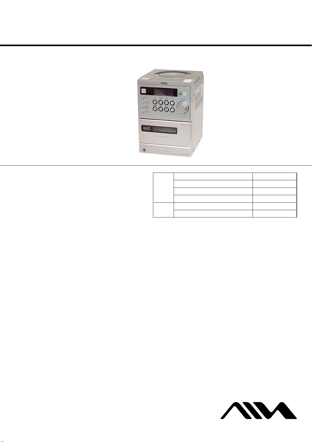
CX-LEM200
SERVICE MANUAL
Ver 1.0 2003.03
CX-LEM200 is the Amplifier, CD player, Tape
Deck and Tuner section in XR-EM200.
CD
Section
TAPE
Section
US Model
AEP Model
UK Model
Model Name Using Similar Mechanism NEW
CD Mechanism Type KSM-213EDP
Base Unit Name BU-K7BD44B
Optical Pick-up Name KSS-213E/C2N
Model Name Using Similar Mechanism NEW
Tape Transport Mechanism T ype CMAL5Z220A
SPECIFICATIONS
TUNER
FM tuning range 87.5 MHz to 108 MHz
FM usable sensitivity (IHF) 16.8 dBf
FM antenna terminal 75 ohms (unbalanced)
US model:
AM tuning range 530 kHz to 1710 kHz (10 kHz step)
AEP and UK models:
MW tuning range 531 kHz to 1602 kHz
AM usable sensitivity 350 µV/m
AM antenna Loop antenna
AMPLIFIER
AUDIO POWER SPECIFICATIONS:
(U.S.A. model only)
POWER OUTPUT AND TOTAL HARMONIC DISTORTION:
With 6-ohm loads, both channels driven, from 100 - 10,000 Hz;
rated 10 W per channel minimum RMS power, with no more than
10% total harmonic distortion from 250 mW to rated output.
Power output
(AEP and UK models)
Input AUX IN: 800 mV
Outputs SPEAKERS: 6 Ω or more
CASSETTE DECK
Track format 4 tracks, 2 channels stereo
Frequency response 50 Hz – 10000 Hz
Recording system AC bias
Heads Recording/playback × 1, erase × 1
531 kHz to 1710 kHz (9 kHz step)
Rated: 8 W + 8 W(6 Ω, T.H.D. 1 %,
1 kHz/DIN 45500)
Reference: 10 W + 10 W(6 Ω, T.H.D.
10 %, 1 kHz/DIN 45324)
MUSIC POWER
20 W + 20 W
PHONES: 32 Ω or more
CD PLAYER
Laser Semiconductor laser (λ = 780 nm)
D/A converter 1 bit dual
Signal-to-noise ratio 95 dB (1 kHz, 0 dB)
Wow and flutter Unmeasurable
GENERAL
Power requirements
US model:
AEP and UK models: 230 V AC, 50/60 Hz
Power consumption 40 W
Power consumption in standby mode
Dimensions (w/h/d) Approx. 163 × 230.5 × 243 mm
Mass Approx. 3.0 kg
Supplied accessories: FM antenna (1)
Specifications and external appearance are subject to change
without notice.
Emission duration: continuous
120 V AC, 60 Hz
with ECO mode on: 0.3 W
with ECO mode off: 6 W
AM antenna (1)
Remote commander (1)
Batteries (2)
MICRO HI-FI COMPONENT SYSTEM
9-877-164-01
2003C167800-1
© 2003.03
Sony Corporation
Home Audio Company
Published by Sony Engineering Corporation

CX-LEM200
TABLE OF CONTENTS
1. SERVICING NOTES ······················································· 3
2. GENERAL ·········································································· 5
3. DISASSEMBLY
3-1. Rear Cabinet ··································································· 7
3-2. CD Cabinet Section, Front Panel Section ······················· 8
3-3. CD Mechanism Deck······················································8
3-4. CONTROL Board···························································9
3-5. Tape Mechanism Deck ···················································· 9
3-6. Cassette Door Assy ······················································· 10
3-7. POWER Board, MAIN Board ······································10
3-8. Optical Pick-up (KSS-213E/C2N)································11
4. MECHANICAL ADJUSTMENTS ····························· 12
5. ELECTRICAL ADJUSTMENTS ······························· 12
6. DIAGRAMS······································································ 15
6-1. Block Diagram – CD Section – ··································· 17
6-2. Block Diagram – Main Section – ································ 18
6-3. Printed Wiring Board – CD Section – ·························19
6-4. Schematic Diagram – CD Section – ····························20
6-5. Printed Wiring Boards – Main Section –····················· 21
6-6. Schematic Diagram – Main Section – ························· 22
6-7. Printed Wiring Board – Control Section –··················· 23
6-8. Schematic Diagram – Control Section –······················ 24
6-9. Printed Wiring Board – Power Section – ·····················25
6-10. Schematic Diagram – Power Section –······················ 26
6-11. IC Pin Function Description ·······································28
7. EXPLODED VIEWS
7-1. Cabinet Section ····························································· 30
7-2. Front Panel Section ······················································· 31
7-3. CD Cabinet Section ······················································ 32
7-4. KSM-213EDP ······························································· 33
8. ELECTRICAL PARTS LIST ······································· 34
2
SECTION 1
r
SERVICING NOTES
CX-LEM200
Notes on chip component replacement
•Never reuse a disconnected chip component.
• Notice that the minus side of a tantalum capacitor may be damaged by heat.
Flexible Circuit Board Repairing
•Keep the temperature of the soldering iron around 270 ˚C during
repairing.
• Do not touch the soldering iron on the same conductor of the
circuit board (within 3 times).
• Be careful not to apply force on the conductor when soldering or
unsoldering.
SAFETY CHECK-OUT
After correcting the original service problem, perform the following
safety check before releasing the set to the customer:
Check the antenna terminals, metal trim, “metallized” knobs, screws,
and all other exposed metal parts for AC leakage.
Check leakage as described below.
LEAKAGE TEST
The AC leakag e from any exposed metal part to earth ground and
from all exposed metal parts to any exposed metal part having a
return to chassis, must not exceed 0.5 mA (500 microamperes.).
Leakage current can be measured by any one of three methods.
1. A commercial leakage tester , such as the Simpson 229 or RCA
WT-540A. Follow the manufacturers’ instructions to use these
instruments.
2. A battery-operated AC milliammeter. The Data Precision 245
digital multimeter is suitable for this job.
3. Measuring the voltage drop across a resistor by means of a V OM
or battery-operated A C voltmeter . The “limit” indication is 0.75
V, so analog meters must have an accurate low-voltage scale.
The Simpson 250 and Sanwa SH-63Trd are examples of a
passive VOM tha t is suitable. Nearly all battery operated digital
multimeters that have a 2 V A C range are suitable. (See Fig. A)
CAUTION
Use of controls or adjustments or performance of procedures
other than those specified herein may result in hazardous
radiation exposure.
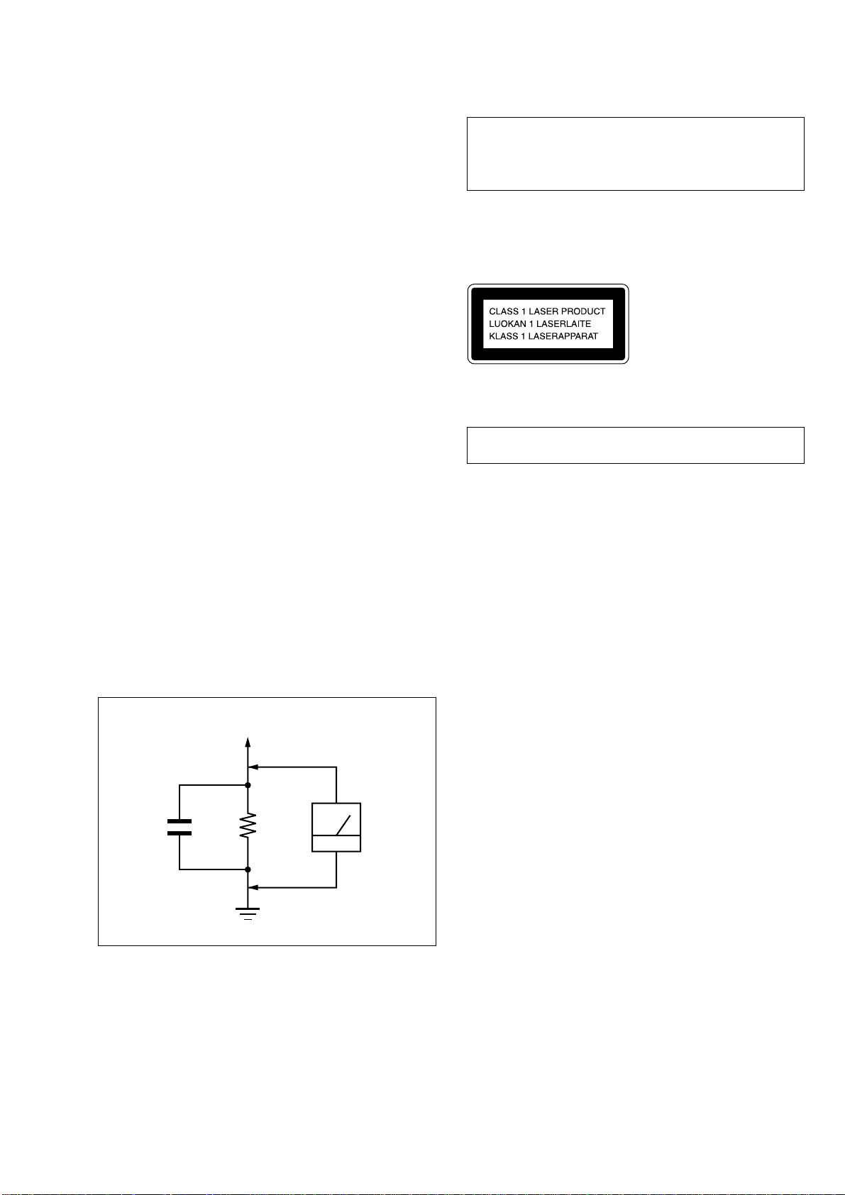
This appliance is classified as a CLASS 1 LASER product.
This label is located on the exterior.
Laser component in this product is capable of emitting radiation
exceeding the limit for Class 1.
NOTES ON HANDLING THE OPTICAL PICK-UP
BLOCK OR BASE UNIT
The laser diode in the optical pick-up block may suffer electrostatic
break-down because of the potential difference generated by the
charged electrostatic load, etc. on clothing and the human body.
During repair, pay attention to electrostatic break-down and also
use the procedure in the printed matter which is included in the
repair parts.
The flexible board is easily damaged and should be handled with
care.
NOTES ON LASER DIODE EMISSION CHECK
The laser beam on this model is concentrated so as to be focused on
the disc reflective surface by the objective lens in the optical pickup block. Therefore, when checking the laser diode emission,
observe from more than 30 cm away from the objective lens.
To Exposed Metal
Parts on Set
1.5 k
0.15 µF
Fig. A. Using an AC voltmeter to check AC leakage.
SAFETY-RELATED COMPONENT WARNING!!
COMPONENTS IDENTIFIED BY MARK 0 OR DOTTED LINE WITH
MARK 0 ON THE SCHEMATIC DIAGRAMS AND IN THE PARTS
LIST ARE CRITICAL TO SAFE OPERATION. REPLACE THESE
COMPONENTS WITH SONY PARTS WHOSE PART NUMBERS
APPEAR AS SHOWN IN THIS MANUAL OR IN SUPPLEMENTS
PUBLISHED BY SONY .
Ω
Earth Ground
AC
voltmete
(0.75 V)
LASER DIODE AND FOCUS SEARCH OPERATION
CHECK
Carry out the “S curve check” in “CD section adjustment” and check
that the S curve waveforms is output three times.
3
CX-LEM200
Service Position of the CD Mechanism Deck
Service Position of the Tape Cassette Mechanism Deck
4
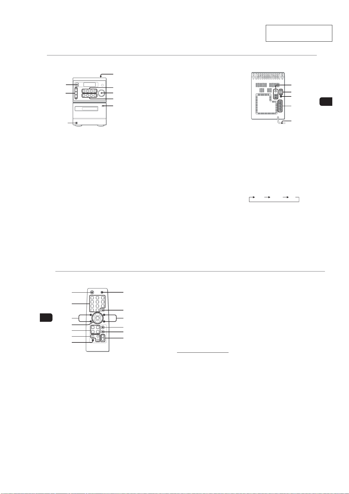
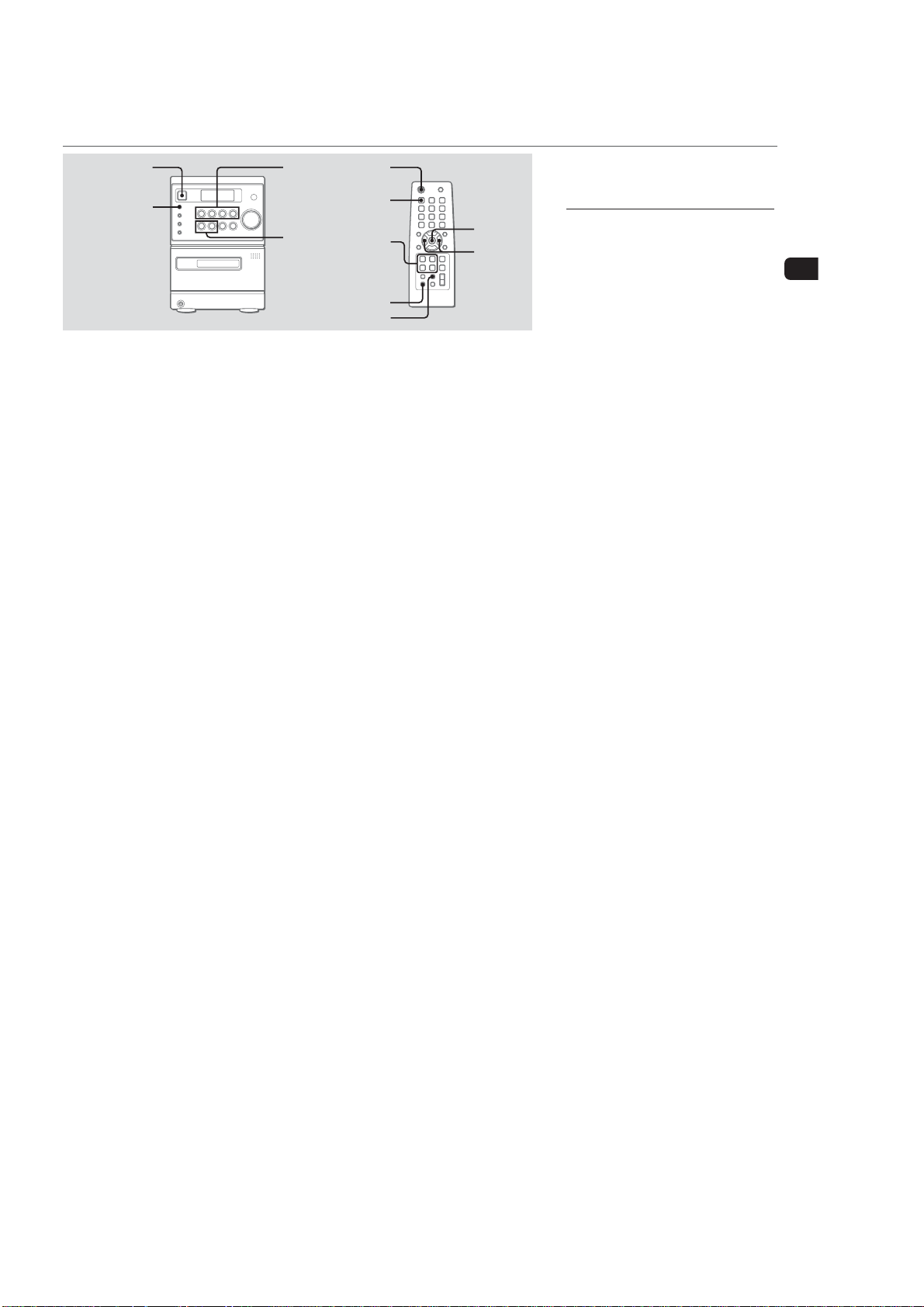
PARTS AND CONTROLS
Main unit: front
Refer to the pages indicated in parentheses for details.
4
1
2
3
1 POWER 6STANDBY/ON (7)
Switches the unit on and off (standby).
2 ECO (7)
Sets the ECO mode on or off.
SYNCHRO REC (13)
Starts recording and CD play simultaneously.
REC START/PAUSE (13)
Starts and pauses recording.
DISPLAY (8)
Changes the display in CD playback mode.
3 PHONES jack
Plug in optional headphones set with a stereo mini plug
(ø3.5 mm). Speaker output is cancelled.
4 OPEN (8)
Opens or closes the disc compartment.
5
6
7
8
SECTION 2
GENERAL
5 ECD (7-9)
Starts and pauses CD play.
TUNER/BAND (7, 10)
Selects tuner function and the tuner band.
cTAPE (REC MUTING) (7, 12, 13)
Starts playback.
Also used to enter 4-second blank spaces during
recording.
AUX (7)
Selects the function of external equipment connected to
AUX IN jacks.
6 VOLUME (11, 14)
Adjusts the volume.
7 f/r-, +t/g (8, 10-12, 14, 15)
CD: skips to a previous or a succeeding track when
pressed, searches a track in fast forward or reverse
playback when held down.
Tape: rewinds or fast forwards the tape.
Tuner: manually tunes up or down within the band.
sSTOP (8, 9, 12, 13)
CD and tape: stops playback.
Tuner: clears a preset station.
TONE (11)
Adjusts the bass or treble level.
8 zPUSH EJECT (12, 13)
Opens or closes the cassette holder.
CX-LEM200
This section is extracted
from instruction manual.
Main unit: rear
Refer to the pages indicated in parentheses for details.
1
2
3
4
5
1 AM jack and FM 75 Ω terminal (4)
Plug in the supplied AM and FM antennas.
2 AUX IN jacks
Accept analogue sound signals from external equipment.
Connect external equipment using an optional connecting
cable with RCA phono plugs (red plug to R jack, white
plug to L jack). Refer also to the operating instructions
for your equipment.
To switch function to external input, press AUX.
To change a source name in the display of the
AUX function.
Hold down AUX and press POWER while the power is
on.
AUX VIDEO TV
3 SUB WOOFER jack
Connect optional powered sub woofer with a built-in
amplifier to the jack.
4 SPEAKER terminals (4)
Connect the speaker cords of the supplied speakers.
5 AC power cord (4)
En
5
Remote commander
Refer to the pages indicated in parentheses for details.
1
2
En
3
4
5
6
7
Buttons with the same or similar names on the main unit
basically have the same function.
1 POWER (7)
2 1–10/0, >10 (8-10)
CD: selects a track of the specified number.
Tuner: tunes in the station with the specified preset
number.
The numbered buttons take on these functions when pressed with
SHIFT held down
CLOCK (7)
Selects clock mode.
TIMER (14)
Selects timer mode.
TUNER MODE (10)
Switches between stereo or monaural FM reception.
:
8
9
0
!
@
#
3 SHUFFLE/PROGRAM (8, 9)
Selects shuffle or programmed CD playback mode.
REPEAT (8)
Selects repeat CD playback mode.
4 PRESETN,M (10)
f/r,t/g (8, 10-12, 14, 15)
ENTER (7, 10, 14, 15)
Determines the mode.
Stores the received station to preset.
5 ECD (7-9)
TUNER/BAND (7, 10)
dTAPE (7, 12)
Starts playback but cannot change the playback side.
AUX (7)
6 DISPLAY (8)
Changes the display in CD playback mode.
DIMMER (7)
Adjusts the display window brightness.
SLEEP (14)
Selects sleep-timer mode.
7 SHIFT
Hold down when pressing a numbered button to change
its function to that printed above the number.
8 MUTING (11)
To turn off the sound temporarily.
9 CLEAR (9, 10, 15)
CD: Clears a CD program.
Tuner: Clears a preset station.
0 TREBLE (11)
Adjusts the treble level.
BASS (11)
Adjusts the bass level.
! s (8, 9, 12, 13)
@ FUNCTION (13)
Switches the active function among TAPE, TUNER, AUX
(VIDEO or TV) and CD.
# VOLUME +,- (11)
6
5
CX-LEM200
ADJUSTMENTS BEFORE OPERATION
POWER
6STANDBY/ON
ECO
Power
Tur ning the unit on
Press POWER 6STANDBY/ON (POWER on the remote ).
Alternatively, press cTAPE, TUNER/BAND, AUX or ECD.
Playback will start automatically if a disc or tape is loaded.
Tur ning the unit off
Press POWER 6STANDBY/ON again.
The unit goes into standby.
Dimmer
The display window brightness can be selected.
Press DIMMER on the remote repeatedly.
Each press of the button changes the following three levels:
"DIMMER 1", "DIMMER 2" and "DIMMER 0".
"DIMMER 0" is the brightest.
ECD,
TUNER/
BAND,
cTAPE,
AUX
f,g
POWER
dTA PE,
DIMMER
ECO mode
Reduces power consumption in standby mode with the following
operations.
Press ECO.
Each press of the button changes the mode as follows;
ECO ON: Power economizing mode is activated.
When the unit turns off, everything in the display disappears
and only the red indicator above POWER lights to show that
the power is being supplied.
ECO OFF: Power economizing mode is cancelled.
When the unit turns off, the clock display appears.
Initial mode is ECO OFF.
Standby power consumption
ECO ON: 0.3 W
ECO OFF: 6 W
CLOCK
ECD,
TUNER/
BAND,
AUX
SHIFT
ENTER
f,g
Setting the clock
1
In stop mode, hold down SHIFT and press CLOCK
on the remote.
Go to step 3 when the hour of the clock display flashes.
2
Within 6 seconds, press ENTER.
The hour flashes in the display.
3
Press f or g to set the hour, then press
ENTER.
4
Press f or g to set the minute.
Each press changes the time in 1-minute steps.
5
Press ENTER.
The time display stops flashing and the clock starts from
00 seconds.
To display the time while the power is on
Hold down SHIFT and press CLOCK on the remote.
The time will be displayed for 6 seconds.
If "- -:- -" appears when the unit is turned off
There has been a power interruption. Reset the clock.
En
7
6
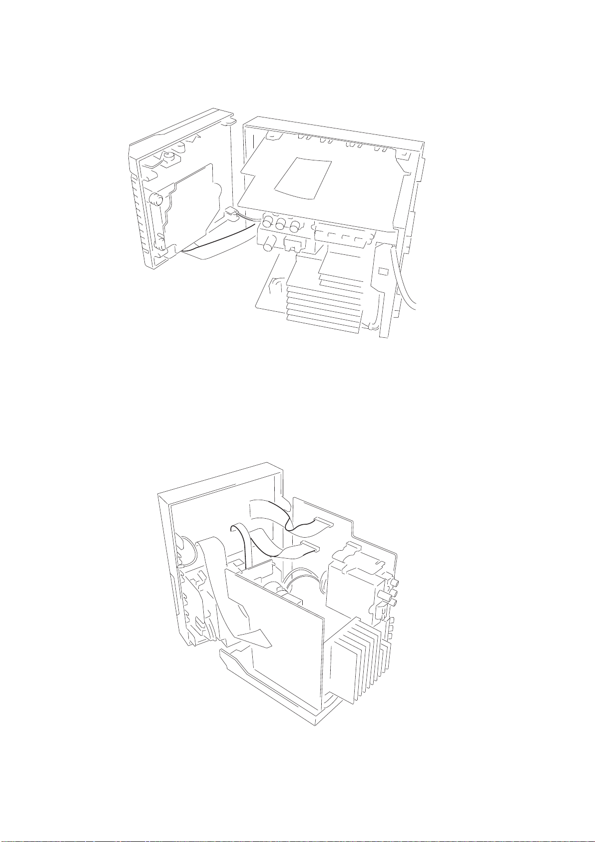
• This set can be disassembled in the order shown below.
)
SET
REAR CABINET
CD CABINET SECTION,
FRONT PANEL SECTION
CX-LEM200
SECTION 3
DISASSEMBLY
CD MECHANISM DECK
(KSM-213EDP)
OPTICAL PICK-UP
(KSS-213E/C2N)
Note: Follow the disassembly procedure in the numerical order given.
CONTROL BOARD POWER BOARD , MAIN BOARD
3-1. Rear Cabinet
5
two screws
(+K3 × 5)
TAPE MECHANISM DECK
(CMAL5Z220A)
CASSETTE DOOR ASSY
7
rear cabinet
1
two screws
(+BVTP3 × 10)
2
five screws
(+BVTP3
3
×
10)
two screws
(+BVTP3 × 10)
6
two screws
(+K3 × 5)
4
two screws
(+BVTP3 × 10
7
CX-LEM200
)
)
3-2. CD Cabinet Section, Front Panel Section
1
connector
(S800)
4
claw
3
claw
6
21p (CN303)
2
w
ire (flat type)
21p (CN101)
w
ire (flat type)
5
CD cabinet section
q;
two screws
(+BVTP3 × 10
qs
claw
qd
front panel section
3-3. CD Mechanism Deck
qa
claw
7
w
ire (flat type)
19p (CN302)
8
connector
(CN301)
9
screw
(+BVTP3 × 10)
3
two vibration proof rubbers (PNK
1
two screws
4
two vibration proof rubbers (GRN)
2
two screws
(+PSW2.6 × 10)
5
CD mechanism deck
(+PSW2.6
×
10)
8
3-4. CONTROL Board
)
)
1
knob volume
3
4
CONTROL board
three screws
(+BTP3
×
10)
2
four screws
(+BVTP3
CX-LEM200
×
10
3-5. Tape Mechanism Deck
1
w
ire (flat type) 7p (CN101)
2
three screws
(+BVTP3
3
tape mechanism deck
×
10
9
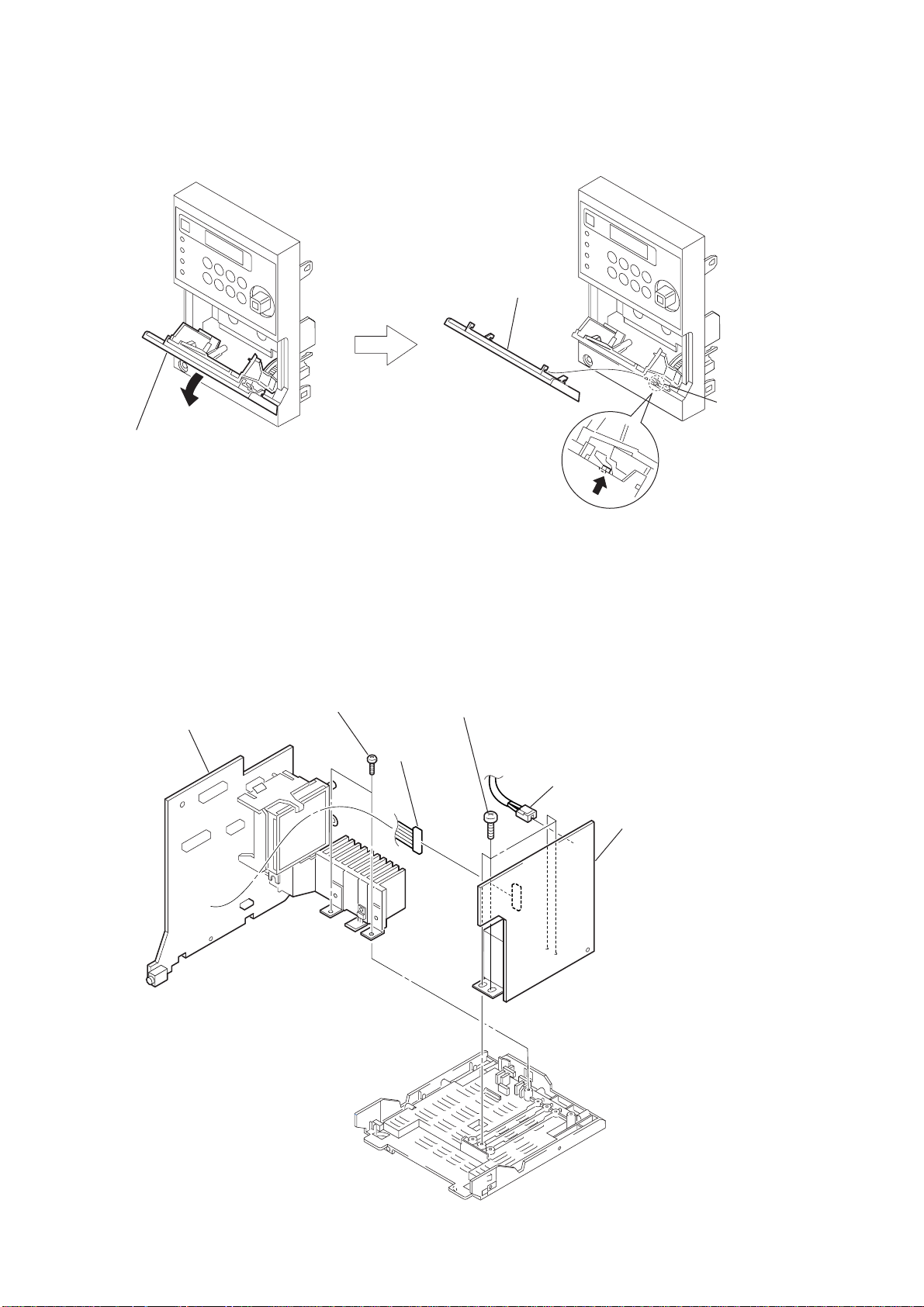
CX-LEM200
w
d
3-6. Cassette Door Assy
1
Open the cassette door assy.
3
cassette door assy
cla
3-7. POWER Board, MAIN Board
5
6
MAIN board
two screws
(+BVTP3
×
10)
2
connector
(CN901)
3
four screws
(+BVTP4
×
12)
1
connector
(AC IN)
2
4
POWER boar
10
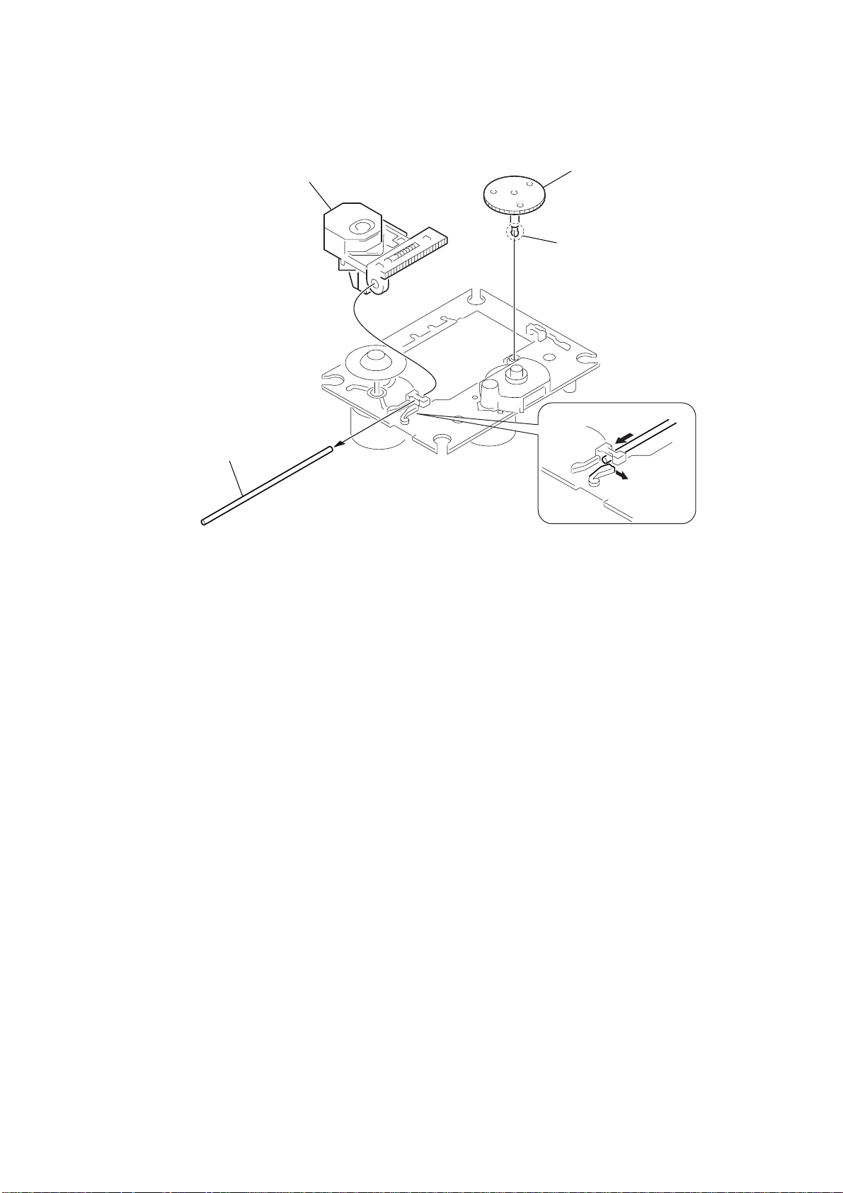
3-8. Optical Pick-up (KSS-213E/C2N)
6
KSS-213E/C2N
5
sled shaft
1
2
gear (A)
claw
CX-LEM200
4
3
11
CX-LEM200
SECTION 4
MECHANICAL ADJUSTMENTS
SECTION 5
ELECTRICAL ADJUSTMENTS
• TAPE MECHANISM DECK SECTION
Precaution
1. Clean the following parts with a denatured alcohol-moistened
swab:
record/playback heads pinch rollers
erase head rubber belts
capstan idlers
2. Demagnetize the record/playback head with a head demagnetizer.
3. Do not use a magnetized screwdriver for the adjustments.
4. After the adjustments, apply suitable locking compound to the
parts adjusted.
5. The adjustments should be performed with the rated power
supply voltage unless otherwise noted.
Torque Measurement
Mode
FWD
FWD
back tension
FF/REW
FWD tension
Torque meter
CQ-102C
CQ-102C
CQ-201B
CQ-403A
Meter reading
2.94 mN • m to 7.84 mN • m
31 to 71 g • cm
(0.43 – 0.98 oz • inch)
0.14 mN • m to 0.59 mN • m
2 to 6 g • cm
(0.02 – 0.08 oz • inch)
6.86 mN • m to 17.64 mN • m
71 to 143 g • cm
(0.98 – 1.99 oz • inch)
more than 0.98 N • m
100 g or more
(3.53 oz or more)
DECK SECTION
Precaution
1. Demagnetize the record/playback head with a head demagnetizer.
2. Do not use a magnetized screwdriver for the adjustments.
3. After the adjustments, apply suitable locking compound to the
parts adjust.
4. The adjustments should be performed with the rated power
supply voltage unless otherwise noted.
5. The adjustments should be performed in the order given in
this service manual. (As a general rule, playback circuit adjustment should be completed before performing recording
circuit adjustment.)
6. The adjustments should be performed for both L-CH and RCH.
7. Switches and controls should be set as follows unless otherwise specified.
•Test T ape
Tape Signal Used for
P-4-A100 10 kHz, – 10 dB Azimuth Adjustment
WS-48B 3 kHz, 0 dB Tape Speed Check
0 dB = 0.775 V
12
CX-LEM200
)
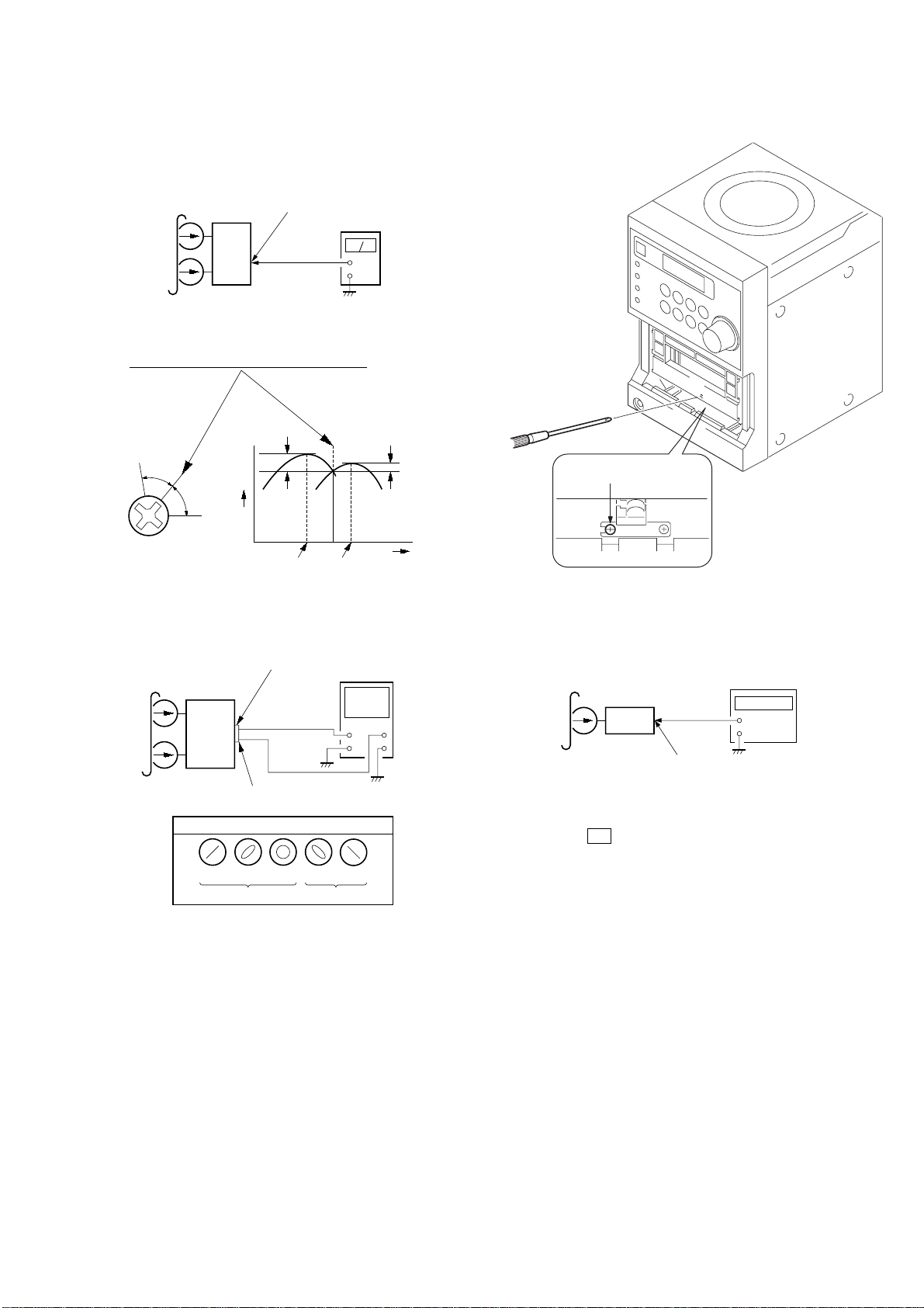
Note: Refer to “3-6. Cassette Door Assy” (see page 10)
adjustment screw
Record/Playback Head Azimuth Adjustment
Procedure:
1. Mode: Playback
test tape
P-4-A100
(10 kHz, – 10 dB)
MAIN board
SPEAKER terminal (J302
L-CH, R-CH
set
level meter
+
–
2. T urn the adjustment screw and check output peaks. If the peaks
do not match for L-CH and R-CH, turn the adjustment screw
so that outputs match within 1dB of peak.
Output
level
within
1dB
L-CH
peak
R-CH
peak
within
1dB
Screw
position
L-CH
peak
Screw
position
R-CH
peak
Adjustment Location:Record/Playback/Erase Head
3. Mode: Playback
MAIN board
test tape
P-4-A100
(10 kHz, – 10 dB)
L-CH
set
R-CH
in phase 45°90°135°180
SPEAKER terminal (J302)
L-CH
R-CH
waveform of oscilloscope
good
oscilloscope
wrong
H
V
°
4. After the adjustments, apply suitable locking compound to the
parts adjusted.
Tape Speed Check
Mode: Playback
test tape
WS-48B
(3 kHz, 0 dB)
set
MAIN board
SPEAKER terminal (J302)
L-CH, R-CH
frequency counter
+
–
1. Insert the WS-48B into the deck.
2. Press the N button on the deck.
3. Confirm that the frequency counter reads 3,000 ± 90 Hz.
Sample value of Wow and Flutter: 0.3% or less W.RMS (JIS)
(WS-48B)
13

CX-LEM200
+
–
CD board
TP (RFAC)
TP (VC)
oscilloscope
CD SECTION
Note:
1. CD Block is basically designed to operate without adjustment. Therefore, check each item in order given.
2. Use YEDS-18 disc (3-702-101-01) unless otherwise indicated.
3. Use an oscilloscope with more than 10MΩ impedance.
4. Clean the object lens by an applicator with neutral detergent when the
signal level is low than specified value with the following checks.
S-curve Check
Connection:
oscilloscope
CD board
TP (FE)
TP (DVC)
Procedure:
1. Connect an oscilloscope to test point TP (FE) and TP (DVC)
on the CD board.
2. Turn the power on.
3. Put the disc (YEDS-18) in and turned power switch on again
and actuate the focus search. (actuate the focus search when
disc table is moving in and out)
4. Check the oscilloscope waveform (S-curve) is symmetrical
between A and B. And confirm peak to peak level within 2 ± 1
Vp-p.
S-curve waveform
+
–
symmetry
A
B
within 2
±
1 Vp-p
RFDC signal waveform
VOLT/DIV: 200 mV
TIME/DIV: 500 ns
±
level: 0.7
0.2 Vp-p
Checking Location: CD board (Conductor side)
RFAC Level Check
Connection:
Procedure:
1. Connect an oscilloscope to test point TP (RFA C) and TP (VC)
on the CD board.
2. Turn the power on.
3. Put the disc (YEDS-18) in to playback the number five track.
4. Confirm that oscilloscope waveform is clear and check RF AC
signal level is correct or not.
Note: A clear RFAC signal waveform means that the shape “◊” can be
clearly distinguished at the center of the waveform.
RFAC signal waveform
VOLT/DIV: 200 mV
TIME/DIV: 500 ns
Note: •Try to measure several times to mak e sure than the ratio of A : B
or B : A is more than 10 : 7.
•Take sweep time as long as possible and light up the
brightness to obtain best waveform.
Checking Location: CD board (Conductor side)
RFDC Level Check
Connection:
oscilloscope
CD board
TP (RFDC)
TP (DVC)
+
–
Procedure:
1. Connect an oscilloscope to test point TP (RFDC) and TP (DVC)
on the CD board.
2. Turn the power on.
3. Put the disc (YEDS-18) in to playback the number five track.
4. Confirm that oscilloscope waveform is clear and check RFDC
signal level is correct or not.
Note: A clear RFDC signal waveform means that the shape “◊” can be
clearly distinguished at the center of the waveform.
level: 0.9
Checking Location: CD board (Conductor side)
Checking Location:
– CD BOARD (Conductor Side) –
TP (VC)
IC103
TP
(RFAC)
TP (FE)
TP (TE)
TP
(DVC)
IC101
TP
(RFDC)
±
0.4 Vp-p
14

• Circuit Boards Location
CX-LEM200
SECTION 6
DIAGRAMS
CONTROL board
MAIN board
CD board
POWER board
REGULATOR board
THIS NOTE IS COMMON FOR PRINTED WIRING
BOARDS AND SCHEMATIC DIAGRAMS.
(In addition to this, the necessary note is printed
in each block.)
For schematic diagrams.
Note:
• All capacitors are in µF unless otherwise noted. pF: µµF
50 WV or less are not indicated except for electrolytics
and tantalums.
• All resistors are in Ω and 1/
specified.
f
•
• 2 : nonflammable resistor.
• 1 : fusible resistor.
• C : panel designation.
Note: The components identified by mark 0 or dotted line
• A : B+ Line.
• B : B– Line.
•Voltages are taken with a V OM (Input impedance 10 MΩ).
•Waveforms are taken with a oscilloscope.
• Circled numbers refer to waveforms.
• Signal path.
: internal component.
with mark 0 are critical for safety.
Replace only with part number specified.
Voltage var iations may be noted due to normal production tolerances.
Voltage var iations may be noted due to normal production tolerances.
F : TUNER
J : CD
d : AUX
E : PB (TAPE)
a : REC (TAPE)
4
W or less unless otherwise
For printed wiring boards.
Note:
• X : parts extracted from the component side.
• Y : parts extracted from the conductor side.
f
•
• : Pattern from the side which enables seeing.
: internal component.
15

CX-LEM200
1.1Vp-p
1 IC103 qg (RFAC)
(CD Play Mode)
2 IC101 el (FE)
(CD Play Mode)
200mV/DIV,
1 µs
/DIV
50mV/DIV,
200 µs
/DIV
100mV/DIV,
200 µs
/DIV
1V/DIV,
20ns
/DIV
200mVp-p
250mVp-p
3 IC101 ra (TE)
(CD Play Mode)
4 IC101 yj (XTAO)
5.4Vp-p
59ns
7
Q307 collector (Rec mode)
5V/DIV,
4 µs
/DIV
14.1Vp-p
10.7
µ
s
•Waveforms
– CD Board –
– CONTROL Board – – MAIN Board –
5
IC801 qd (32.768kHz)
30.5
µ
s
1V/DIV,
10 µs
/DIV
6
IC801 qh (8.6MHz-EXTAL)
116ns
1V/DIV,
40ns
/DIV
5.4Vp-p
4.0Vp-p
16

6-1. Block Diagram – CD Section –
CX-LEM200
DETECTOR
A
B
C
D
I-V AMP
F
E
OPTICAL PICK-UP
BLOCK
KSM-213EDP
LASER DIODE
PD
LD
(SPINDLE)
CD +5V
Q101
AUTOMATIC
POWER
CONTROL
M
A
6
B
7
C
8
D
9
F
11
F I-V AMP
E
10
E I-V AMP
LD
1
FOCUS/TRACKING COIL DRIVE,
SPINDLE/SLED MOTOR DRIVE
CH4OUTF
15
16
CH4OUTR
MOTOR
DRIVE
IC102
FOCUS/TRACKING ERROR AMP
RF
SUMMING
AMP
FOCUS
ERROR AMP
RF DC
AMP
TRACKING
ERROR AMP
APC LD
AMP
CH4SIN
25
AC
SUM
RFDCO
RFDCI
SW
IC103
RF AMP,
FE
FEI
TE
PD
FILTER
53
54 56
FILO
EQ
IN
4
16
17
28
29
18
12
2
RFAC
3
VCA
RFAC
EQ
15
PWM3
PWM2
RFAC
51
49
48
ASYMMETRY
CORRECTION
ASYI
ASYO
DIGITAL
CLV
MDP
XRST
26 7 8
3
SUBCODE
PROCESSOR
XLON
DATA
CLOK
14 5
PCO
CLTV
DIGITAL
PLL
CPU INTERFACE
XLAT
SENS
6
94 3
87
C-DATA
97
C-CLK
C-XLT
86
C-LDOM
95
55
FILI
DEMODULATOR
SERVO AUTO
SEQUENCER
SCOR
20
C-SENS
S-SCOR
SQSO
1 2
96 88
IC101 (1/2)
DIGITAL SIGNAL PROCESSOR,
DIGITAL FILTER, D/A CONVERTER
16K
RAM
EFM
INTERNAL BUS
ERROR
CORRECTOR
SERVO
INTERFACE
SSTP
SQCK
C-SQCK
C-SQSO
SCLK
9 21
COUT
EMPH
64 15
27
S101
(LIMIT)
D/A
INTERFACE
WFCK
GFS
18
Q102
+3.3V
REG
PCMD
BCK
LRCK
C2PO
SERIAL
IN
INTERFACE
TO MIRR/DFCT/
FOK DETECTOR
+5V
62
63
61
19
NOISE SHAPER
+7V
Q317
CD +5V
REG
DIGITAL
FILTER,
DIGITAL
OUT
60
DOUT
+7V
PWM
&
INTEGRATOR
AOUT1
AOUT2
70
77
71
76
CLOCK
GENERATOR
AIN1
AIN2
BUFFER
TIMING
LOGIC
LOUT1
LOUT2
XTAI
XTAO
72
75
66
67
CD
L-CH
R-CH
X101
16.9344MHz
A
MAIN SECTION
2-AXIS
DEVICE
(TRACKING)
(FOCUS)
(SLED)
PWM2
43
39
40
41
FE
TE
SE
M
18
11
12
13
14
CH3OUTR
CH2OUTR
CH2OUTF
CH1OUTR
CH1OUTF
CH3OUTF
17
MOTOR
DRIVE
COIL
DRIVE
COIL
DRIVE
CH3FIN
CH3RIN
CH2RIN
CH2FIN
CH1RIN
CH1FIN
MUTE
24
23
SFDR
28
SRDR
29
6
5
3
2
20
TFDR
30
TRDR
31
FFDR
32
33
FRDR
FOCUS/TRACKING/SLED
RFDC
A/D
CONVERTER
PWM GENERATOR
SERVO DSP
FOCUS/TRACKING/SLED
IC101 (2/2)
DIGITAL SERVO
PROCESSOR
MIRR/DFCT/
FOK
DETECTOR
TO SERVO INTERFACE
FOK
MIRR
DFCT
24
22
23
PWM3
1
2
85
C-PWM1
C-PWM2
C-XRST
IC801 (1/2)
SYSTEM CONTROLLER
• Signal Path
: CD
1717

CX-LEM200
6-2. Block Diagram – Main Section –
J303(1/2)
L
AUX IN
R
TUNER PACK
+5V
L-CH
R-CH
D OUT
D IN
CLK
TUNED
STEREO
MUTE
FM SOUT
R DATA
R INT
DECK
L-CH
REC/PB
HEAD
ERASE
HEAD
MECHANISM BLOCK
PLAY
R REC
T END
M1
M
DECK
MOTOR
A
CD SECTION
CD OPEN/CLOSE
S800
(OPEN)
CE
L OUT1
L OUT2
R-CH
+5V
R-CHR-CH
R-CH
T301
BIAS OSC
R-CH
Q309
Q323,325
MOTOR
DRIVE
Q321,322
T SOL
DRIVE
BIAS
OSC
Q307
Q308
Q326-332
REC/PB
SWITCH
+10V
PB/REC EQ AMP
IC302
OUT L
AUX L
19 18
OUT R
TU L
23
TAPE L
2
21
CD L
CONT
REC OUT
IC303
POWER
AMP
6 5
13
D809
D810
D813
12
11
FL -26V
+5.6V (SUB)
TU +5V
Q333
AC
DET
FL -26V
+5.6V( SUB)
IC302
+5V
+5V
(MAIN)
+10V
IC302
-5V
+7V
2
10
F-DATA
98
TU DATA
99
TU COUNT
100
TU CLK
84
TU CE
93
TU TUNED
92
TU STEREO
80
TU MUTE
23
RDS-SIG
91
RDS-DATA
27
RDS-CLK
77
TA REC/PB
12
32.768kHz
13
32.768kHz
15
8.64MHz
16
8.64MHz-EXTAL
74
TA BIAS
79
TA PLAY.SW
24
TA SW
5
TA END
6
TA MOTOR
4
TA SOL
76
C-DOOR
SYSTEM CONTROL
IC801 (2/2)
AMP MUTE
AMP-STNBY
SEG20
GRID1
GRID8
VOL.ENC
I POWER DOWN
I POWER MONITOR
POWER ON
SEG1
RST
9
78
FL801
FLUORESCENT
DISPLAY
45
.
47
50
.
52
66
37
44
18KEY1
19KEY2
22
75ECO.LED
29RMC
11
20
26
CD
82
8
F1 F2
S801-806
FUCTION
KEY
S807-813
FUCTION
KEY
RV801
VOL
ENCODER
D811
ECO
IC802
REMOTE
CONTROL
RECEIVER
µCON +B
µCON +B
Q815
RESET
SWITCH
31
IC803
RESET
POWER
MONITER
Q338
R-CH
16
13
28
X801
32.768kHz
X802
8.64MHz
R-CH
R-CH
Q310
+5V
REG
Q305
+5V
REG
Q339
+5V
REG
Q306
-5V
REG
Q334-337
FL -26V
REG
Q320
CD POWER
CONTROL
Q315
POWER
CONTROL
J303(2/2)
POWER AMP
Q319
+7V
REG
D317
Q312-314
+5.6V
REG
VCC
IC305
+10V
RE
HEADPHONES
L
J302
SPEAKER
R
SUB
WOOFER
D319-321
13
+10V
Q311 RY801
RELAY
DRIVE
J301
• R-CH is omitted due to same as L-CH.
• Signal Path
: TUNER
: CD
: AUX
: PB (TAPE)
: REC (TAPE)
T902
POWER
TRANSFORMER
D916-919
D911-914
D922-925
F1(AC 3.5V)
F2(AC 3.5V)
D907-910
(MAIN)
T901
POWER
TRANSFORMER
(SUB)
LF901
LINE
FILTER
AC
IN
1818

CX-LEM200
6-3. Printed Wiring Board – CD Section –
A
B
C
• See page 15 for Circuit Boards Location.
• Semiconductor
Location
Ref. No. Location
D101 F-5
IC101 E-4
IC102 C-5
IC103 D-2
Q101 C-2
Q102 G-5
TP (VC)
IC102
D
E
F
IC103
TP (RFAC)
TP (DVC)
IC101
CONTROL
CN803
23
G
12
1-680-849-
345678
1919

CX-LEM200
6-4. Schematic Diagram – CD Section –
• See page 16 for Waveforms. • See page 26 for IC Block Diagrams.
KSM-213EDP
CONTROL
CN803
0uH
0uH
24
2020

CX-LEM200
6-5. Printed Wiring Boards – Main Section –
L
AUX IN
R
SUB
WOOFER
+
L
-
IMPEDANCE
USE6-16
SPEAKER
+
R
• See page 15 for Circuit Boards Location.
TUNER
PACK
IC302
IC303
TO
CONTROL
BOARD
CN802
(Page 23)
18
TO
CONTROL
BOARD
CN805
(Page 23)
HEAD
(REC/PLAY/ERASE)
L-CH
REC/PB
R-CH
ERASE
• Semiconductor
Location
Ref. No. Location
D301 E-5
D302 C-4
D303 B-7
D304 C-5
D305 E-4
D306 F-4
D310 E-4
D311 B-4
D312 A-6
D313 A-6
D317 E-5
D318 E-6
IC302 C-3
IC303 F-2
Q305 E-4
Q306 F-4
Q307 D-5
Q308 D-5
Q309 D-5
Q310 B-4
Q311 F-5
Q312 E-4
Q313 E-5
Q314 E-4
Q315 E-5
Q317 A-6
Q319 A-6
Q320 B-6
Q321 A-5
Q322 B-5
Q323 A-4
Q325 B-4
Q326 D-4
Q327 D-4
Q328 C-4
Q329 C-4
Q330 C-4
Q331 C-4
Q332 C-4
Q333 F-5
Q334 E-6
Q335 F-6
Q336 F-6
Q337 F-6
Q338 E-6
Q339 C-5
-
TO
POWER
BOARD
CN901
(Page 25)
PHONES
IC305
2121

CX-LEM200
6-6. Schematic Diagram – Main Section –
J303
10k
R236
C226
R237
220p
4.7k
C126
R137
220p
4.7k
R136
10k
8.2k
1000p
C101
R101
5.6k
T301
BIAS OSC
Q329
2SK2158
2SK2158
C315
47 25V
R208
8.2k
R108
39k
R102
Q328
Q327
KTA1504
Q326
KTA1504
R309
4.7
Q307
KTC3205Y-A
C317
1000p
R311
22k
CN301
7P
1000p
C201
R201
5.6k
C318
0.01
R314
5.6k
C314
0.012
• See page 16 for Waveform. • See page 27 for IC Block Diagrams.
R225
22k
R125
C227
470p
C127
470p
C109
470p
BD3881FV
C102
1000p
R319
1SS133T-77
C316
6800p
IC302
R103
C312
220p
D302
470p
C209
R112 R212
R109
2.2k
C110
180p
C103
100p
470
R203
39k
R202
Q330
2SK2158
1M
KRA303-RTK
R310
3.3
C112
3.3k
C111
5600p
R115
1k
R113
R114
1.8k
33k 33k
R209
2.2k
R111
2.2k
470
C202
R104
1000p
82
C104
47
10V
Q331
KRA303-RTK
Q332
R312
4.7k
KRC402-RTK
3300p
C212
R214
C210
180p
R105
390k
C313
100 16V
Q308
KTA1271Y
Q309
C217
C117
1200p
1k
1k
3.3k
C211
5600p
3300p
1.8k
R106
5.6k
R217
R215
1k
R213
8.2k
8.2k
R211
2.2k
R116
R216
R205
C203
100p
R204
82
R320
4.7k
R313
47k
C349
22
25V
C107
390k
C106
0.022
150k
R107
C206
R206
5.6k
R207
C204
47
C301
10V
1k
1.5k
1.5k
R117
R221
R219
R119
4.7k
10k
10k
4.7k
R120
R218
R220
R118
50V
50V
2.2
C207
2.2
0.022
150k
10p
R303
4.7k
50V
4.7
C132
1200p
1k
50V
R121
C113
2.2k
R123
0.22
50V
C114
0.47
R122
68k
R222
68k
10k
C208
C108
R301
3300p
3300p
R302
4.7k
47
25V
50V
4.7
C232
22k
R226
22k
R126
22k
470p
C116
C216
470p
50V
2.2k
R223
C213
0.22
C214
0.47
50V
C115
4.7 50V
C344C343
47
25V
C303
C345
100
16V
0.01
KTC3203Y
C133
0.056
C215
4.7 50V
Q305
KTC3203Y-AT
R304
470
25V
C302
22
Q339
D304
MTZJ-T-77-5.6B
R332
C335
D305
1k
0.01
R143
10k
R124
22k
R224
22k
C233
0.056
KTA1271Y-AT
C304
0.01
C305
220
10V
MTZJ-T-77-5.1A
R243
Q306
R305
470
Q317
KTC3205Y
C329
100
16V
D303
MTZJ-T-77-5.6B
10k
C330
220
10V
D306
MTZJ-T-77-5.1A
D312 D313
1N4002 1N4002
R318
470
C331
0.01
IC303
LA4636
0.1
0.1
C310
47
25V
R132
1k
R128
R131
3.3k
3.3k
C118
C134
0.033
2200p
R352
470
Q338
KRC402-RTK
R317
47k
Q319
KTA1271Y-AT
R348
1k
Q320
KRC402-RTK
C332
100
16V
Q321
KTA1271Y-AT
Q322
KRC402-RTK
C348
0.1
C219
C119
4.7
50V
R232
1k
R231
3.3k
C234
2200p
C218
R228
3.3k
0.033
C311
10
50V
R351
10k
50V
C336
D301
22
1SS133
R330
47k
R329
1k
4.7
50V
R306
10k
0.01
C322
R336
4.7k
Q333
KRC402-RTK
KYA1271Y-AT
KRC402-TRK
47k
R357
0.1
C220
2.2
R229
C350
0.047
C228
22 50V
R350
10k
Q323
Q325
R328
47k
R354
R356
0.1
C121
C221
C120
2.2
R321
100k
R238
180
D317
1SS133T-77
R331
47k
C320
0.01
R355
100k
R130
R138
180
C128
22 50V
Q315
KRC402-RTK
50V
C337
22
2.2
R129
Q311
KTA1271Y-AT
25V
C327
47
100k
R337
C324
220
16V
KTC3205Y
C347
0.1
MTZJ-T-77-5.6B
R338
KTA1266-GR-AT
C309
Q310
10
16V
1000
R322
D311
C338
100 10V
25V
C323
4700
D310
MTZJ-T-77-5.6B
1k
Q334
C333
470 16V
R323
1k
Q312
KTC3203Y
R316
470
C319
0.01
Q335
KTA1266-GR-AT
R139
180
Q314
KTA1271Y-AT
C326
2200p
R343
4.7
R345
4.7
R339 R340
4.7k 4.7k
C339
0.01
2.2
R230
R315
2.2k
1k
C328
100
16V
10k
C346
470
16V
Q313
KTC3203Y
Q336
KTA1266-GR-AT
MTZJ-T-77-27B
R240
2.2k
C229R239
C129
22 50V
R325R324
100k2.2k
D318
C342
470 16V
R140
2.2k
22 50V180
R326
100k
R327
10k
R349
JR
R344
3.3
R346
3.3
Q337
KTA1266-GR-AT
R341 R342
4.7k 4.7k
R347
1k
C230 C130
10
50V1050V
C123
1000 16V
22k
22k
R142
R242
L101
L102
L202
C223
L201
1000
16V
CN307
3P
CNP305
10P
0.1
0.1
C341
C340
J302
J301
CNP308
3P
IC305
KIA7809API
CN302
19P
CN303
21P
CN304
11P
2222

CX-LEM200
6-7. Printed Wiring Board – Control Section –
IC802
S800
(OPEN)
RED
WHT
• See page 15 for Circuit Boards Location.
FLUORESCENT INDICATOR TUBE
IC801
(AEP,UK)
(US)
ECO
POWER
STANDBY/ON
• Semiconductor
Location
Ref. No. Location
D803 C-5
D807 D-3
D808 D-2
D809 D-2
D810 D-5
D811 B-6
D812 D-3
D813 D-3
IC801 B-3
IC802 A-1
IC803 D-3
Q815 D-2
TO
CD
BOARD
CN101
(Page 19)
VOLUME
AUX
TONE
STOP
IC803
TAPE
(REC MUTING)
TUNER/BAND
CD
SYNCHRO
REC
ECO
TO
MAIN
BOARD
CN303
(Page 21)
REC START
REC PAUSE
DISPLAY
TAPE MECHANISM
DECK
TO
MAIN
BOARD
CN302
(Page 21)
2323

CX-LEM200
6-8. Schematic Diagram – Control Section –
CNP804
2P
S800
CN803
21P
0.1
C840
0.1
C841
R841
R842R843R844R845R846
2.2k
2.2k1k4.7k47010k
S806
R871
22k
S813
• See page 16 for Waveforms.
C818
C819
1
1
50V
50V
R872
100
R897
100
R839
R840
2.2k
R848R850R851R852R853R854
R849
2.2k2.2k1k4.7k47010k
2.2k
S809S810S811S812
10k
S801S802S803S804S805
R847
10k
S808
S807
FL801
D811
SEL2215S-CD
R892
1k
0.01
C811
R821
10k
C812
100
16V
C814
100 16V
R820
100k
1k
1k
1k
R858
R869
R893
100k
R891
100k
R890
100k
R889
100k
R888
100k
R887
100k
R886
100k
R895
1k
R885
100k
1k
R822
R823
1k
R824
1k
R825
1k
R826
1k
C813
0.01
R827
1k
R828
R829
1k
R830
1k
R831
1k
R832
1k
R833
1k
R834
1k
R835
1k
R836
1k
R870
1k
5.6k
5.6k
R803
R802
R801
C810
0.01
10k
1k
1k
1k
R894
R884
R857
R819
1k
1k
1k
R806
R804
R805
10k
R882
LC876756C-51E4
R810
10M
X801
32.768KHz
C801
24p
C835
R883
2.2k
4.7
50V
390k
R814
24p
C802
IC801
X802
20p
C816
C803
0.01
C804
100 6.3V
100K
RP20
8.64MHz
20p
C817
100K
100K
100K
100K
100K
100K
RP14
RP17
RP15
RP18
RP16
RP19
1k
1k
47k
22k
R808
R807
R809
R811
HNA-08SS49T
100K
100K
100K
100K
100K
100K
RP05
RP03
RP04
100K
100K
100K
100K
100K
100K
100K
100K
RP06
RP07
RP08
RP09
RP10
RP11
RP12
RP13
R818
56k
1k1k1k
18p
R812
R813
C836
R815
220k
IC802
NJL64H380A
C805
16V
47k
1000p
R896
R859
C815
100
RG06
RG07
RG08
RP01
RP02
22
C806
0.01
100K
100K
100K
100K
100K
100K
100K
RG05
RG04
0.01
RG02
RG03
RG01
C807
50V
R880
4.7
10k
C834
R881
2.2k
C809
0.01
C808
100
6.3V
CN802
21P
R860
47k
RV801
0
(AEP,UK)
R856
10k
10k
C820
0.01
866
R
R867
47k
D810
1SS133T-77
D812
R879
22k
C839
0.1
Q815
KTC3875Y
R877
47k
R878
47k
D808
1SS133T-77
D807
R876 R875
1SS133T-77
1k 1k
IC803
CN805
PST592C
19P
C831
0.1
C830
0.1
1SS133T-77
D813
C828
1SS133T-77
470
6.3V
C829
47
25V
D809
1SS133T-77
R868
(US)
R865
10k
C821
R855
0.01
22k
R863 R861
10k 47k
R864
10k
CN801
7P
D803
C822
1SS133T
22
-77
16V
2424

CX-LEM200
6-9. Printed Wiring Board – Power Section – 6-10. Schematic Diagram – Power Section –
• See page 15 for Circuit Boards Location.
C907
C908
(US)
AC
IN
C910
C912
C913
0.022
TO
MAIN
BOARD
CNP305
(Page 21)
T902
POWER
TRANSFORMER
(SUB)
CN901
10P
C914
0.022
R907
100
D916
0.022
D918
1N5401
C905
0.022
1N5401
D919
C906
1N5401
D917
1N4002
1N4002
D923
D924
1N4002B
1N4002B
0.022
1N5401
R901
47k
R902
47k
C909
0.022
D911
1N4002
C911
0.022
D912
1N4002
C915
0.022
C916
0.022
D909
1N4002
D910
1N4002
T902
R911
3.3M
D906
1SS133T-77
D907
1N4002
D908
1N4002
RY901
T901
CN902
2P
LF901
AC IN
0.022
D920
1SS133
D921
1SS133
0.022
D913
D914
0.022
D925
1N4002B
D922
1N4002B
• Semiconductor
Location
Ref. No. Location
D906 B-3
D907 B-3
D908 B-3
D909 A-3
D910 A-3
D911 C-3
D912 C-3
D913 C-3
D914 C-3
D916 A-1
D917 B-1
D918 A-1
D919 B-1
D920 A-2
D921 A-2
D922 D-3
D923 D-3
D924 D-3
D925 D-3
T902
POWER
TRANSFORMER
(MAIN)
2525

CX-LEM200
• IC Block Diagrams
– CD Board –
IC101 CXD3017Q
DIGITAL
OUT
LRCK
61
PCMD
62
INTERFACE
63
BCK
64
EMPH
65
XVDD
XTAI
XTAO
XVSS
AVDD1
AOUT1
AIN1
LOUT1
AVSS1
AVSS2
LOUT2
AIN2
AOUT2
AVDD2
RMUT
LMUT
66
67
68
69
70
71
72
73
74
75
76
77
78
79
80
1
2
SQSO
TIMING
SQCK
IC102 BA5974FP-E2
PRFVCC
DOUT
60
D/A
LOGIC
PWM
3rd ORDER
NOISE SHAPER
OVER SAMPLING
DIGITAL FILTER
SERIAL IN
INTERFACE
3
4
XRST
SYSM
CH4BIN
VDD
59
58
INTERNAL BUS
PWM
CH4SIN'
VSS
AVDD3
57
CH4SIN
ERROR
CORRECTOR
16K
RAM
SUBCODE
PROCESSOR
CH3FIN
F
INTERFACE
FILI
PCO
54
56
55
DIGITAL
PLL
EFM
DEMODULATOR
SERVO
INTERFACE
SERVO AUTO
SEQUENCER
CPU
INTERFACE
7
8
5
6
XLAT
CLOK
DATA
CH3RIN
CAPAIN3
R
R
FILO
53
SENS
CLTV
AVSS3
52
9
SCLK
RFAC
51
50
ASYMMETRY
CORRECTOR
10
11 12
VDD
ATSK
BIAS
49
13
SPOA
ASYI
48
14
SPOB
MUTE
ASYO
XLON
AVDD0
47
46
1516171819
XUGF
WFCK
GND
ADIO
IGEN
AVSS0
45
44
SERVO DSP
FOCUS
SERVO
TRACKING
SERVO
SLED
SERVO
20
GFS
C2PO
XPCK
SCOR
MUTE
202122232425262728 19 18 17 16 15
CE
RFDC
43
41
42
OPERATIONAL
AMPLIFIER
ANALOG SWITCH
A/D
CONVERTER
POWVCC
CH3OUTR
TE
CLOCK
GENERATOR
PWM GENERATOR
FOCUS PWM
GENERATOR
TRACKING
PWM GENERATOR
SLED PWM
GENERATOR
DIGITAL
CLV
MIRR, DFCT,
FOK
DETECTOR
CH3OUTF
CH4OUTR
40
39
38
37
36
35
34
33
32
31
30
29
28
27
26
25
24
23
22
21
CH4OUTF
SE
FE
VC
XTSL
TES1
TEST
VSS
FRDR
FFDR
TRDR
TFDR
SRDR
SFDR
SSTP
MDP
LOCK
FOK
DFCT
MIRR
COUT
IC103 CXA2581N-T4
DVC
VC
APC AMP
DVC
VC
A
B
C
D
APC-OFF
(Hi-Z)
RW/ROM
(H/L)
A
GM
GM
EQ IN
AC SUM
GND
SW
DVCC
DVC
RFAC
1
LD
2
PD
3
4
5
6
A
7
B
8
C
9
D
10
E
11
F
12
13
14
15
–
+
RFAC
SUMMING
AMP
BCD
RW/ROM
30
DC OFST
29
A
B
C
D
VOFST
B
C
A
D
B
D
A
C
DVC
RW/ROM
EQ ON/OFF
RW/ROM
RW/ROM
RW/ROM
RW/ROM
RW/ROM
RW/ROM
–
+
VOFST
–
+
–
+
VOFST
–
+
–
+
DVC
VCC
EQ
RFAC
VCA
VCC
–
+
DVC
VC
VC
–
+
DVC
VC
RFDCI
28
RFDCO
VC
27
VC
26
RFC
25
VFC
24
BST
23
RFG
22
VCC
21
CEI
20
CE
19
TE BAL
18
TE
17
FEI
16
FE
F
RF
CH1RIN
F
RF
CH2RIN
F
R
GND
CAPAIN2
VREFIN
POWVCC
CH2OUTR
R
INTERFACE
CH2FIN
CAPAIN1
INTERFACE
1 2 3 4 5 6 7 8 9 10 11 12 13 14
CH1FIN
VREFOUT
THERMAL
SHUTDOWN
CH2OUTF
LEVEL SHIFT
CH1OUTR
CH1OUTF
2626

– MAIN Board –
IC302 BD3881FV
CX-LEM200
REC-O_L
TAPE-L
TAPE-R
REC-O_R
TUNER-R
TUNER-L
CD-R
CD-L
AUX-R
AUX-L
OUT-L
TON_H-L
TON_L-L
TON_H-R
OUT-R
TON_L-R
VSS
IC303 LA4636
1
2
3
4
5
IN1
IN2
PRE GND
STAND BY
RIPPLE FILTER/
STARTING TIME
+
–
INPUT
AMP
+
–
INPUT
AMP
6
7
VCC
SIGNAL MUTE
OUTPUT
AMP
OUTPUT
AMP
8
+OUT2
9
10
–OUT2
PWR GND2
11
–OUT1
12
+OUT1
27

CX-LEM200
6-11. IC Pin Function Description
• IC801 LC876756C-51E4 (System Control)
Pin No.
1
2
3
4
5
6
7
8
9
10
11
12
13
14
15
16
17
18
19
20
21
22
23
24
25
26
27
28
29
30 to 36
37 to 44
45
46
47 to 50
51
52 to 66
67 to 71
72
73
74
75
76
77
78
79
80
81
82
83
84
Pin Name
C-PWM1
C-PWM2
C-SCOR
TA SOL
TA END
TA MOTOR
HP MUTE
POWER ON
AMP-MUTE
F-DATA
RST
32.768kHz
32.768kHz
GND
8.64MHz
8.64MHz-EXTAL
VDD1
KEY1
KEY2
I POWER DOWN
VERSION
VOL-ENC
RDS-SIG
TA SW
SHT-CLK
I POWER MONITOR
RDS-CLK
A-MUTE
RMC
NC
G1 to 8
SEG1
VDD3
SEG2 to 5
NO-USE
SEG6 to 20
NC
VDD4
BASS+2
TA BIAS
ECO.LED
C-DOOR
TA REC/PB
AMP-STNBY
TA PLAY.SW
TU MUTE
FL-CON
CD
TU
TU CE
I/O
O
PWM1 signal output to the CD unit
O
PWM2 signal output to the CD unit
I
SCOR (SUBQ request) signal output to the CD unit
O
Solenoid control signal output to the tape deck
I
Tape deck reel switch signal input
O
Motor control signal output to the tape deck
O
Not used (open)
O
Power relay control signal output
O
Muting control signal output to the power amplifier
O
Control signal output to the sound processor
I
Reset signal input from the reset IC (IC803)
I
Resonator terminal (32.768kHz)
O
Resonator terminal (32.768kHz)
—
Ground terminal
I
Resonator terminal (8.64MHz)
O
Resonator terminal (8.64MHz)
—
Power supply terminal
I
Key AD input 1
I
Key AD input 2
I
Power down detection signal input
I
Version setting terminal
I
Encoder signal input from the volume encoder
I
RDS signal level input from the tuner
I
Tape switch status signal input from the tape deck
O
Clock shift control signal output
I
AC detection signal input
I
RDS clock input from the tuner
—
Not used
I
Remote sensor signal input
—
Not used (open)
O
Grid signal output to the fluorescent indicator tube
O
Segment signal output to the fluorescent indicator tube
—
Power supply terminal
O
Segment signal output to the fluorescent indicator tube
—
Ground terminal
O
Segment signal output to the fluorescent indicator tube
—
Not used (open)
—
Power supply terminal
—
Not used (fixed at “H”)
O
Bias control signal output to the bias oscillation circuit
O
ECO LED control signal output
O
CD door open/close switch signal input
O
REC/PLAY control signal output to the REC/PLAY switch circuit
O
Standby control signal output to the power amplifier
I
Play switch signal input from the tape deck
O
Muting signal output to the tuner
—
Not used (open)
O
CD power supply control signal output
O
Not used (open)
O
Tuner chip enable signal output to the tuner
Description
28

CX-LEM200
Pin No.
85
86
87
88
89
90
91
92
93
94
95
96
97
98
99
100
Pin Name
C-XRST
C-XLT
C-DATA
C-SQCK
GND
VDD2
RDS-DATA
TU STEREO
TU TUNED
C-SENS
C-LDON
C-SQSO
C-CLK
TU DATA
TU COUNT
TU CLK
I/O
O
Reset signal output to the CD unit
O
Latch signal output to the CD unit
O
Data output to the CD unit
O
SUBQ clock output to the CD unit
—
Ground terminal
—
Power supply terminal
I
RDS data input from the tuner
I
Stereo/mono detection signal input from the tuner
I
Tuner tuned status signal input
I
SENS signal input from the CD unit
O
LD ON signal output to the CD unit
I
SUB-Q data input from the CD unit
O
Clock output to the CD unit
O
Data output to the tuner
I
IF count signal input from the tuner
O
Clock signal output to the tuner
Description
29

CX-LEM200
3
NOTE:
• -XX, -X mean standardized parts, so they may
have some differences from the original one.
• Items marked “*” are not stocked since they
are seldom required for routine service. Some
delay should be anticipated when ordering these
items.
7-1. Cabinet Section
SECTION 7
EXPLODED VIEWS
• The mechanical parts with no reference number
in the exploded views are not supplied.
CD cabinet section
The components identified by mark 0 or
dotted line with mark 0 are critical for safety.
Replace only with part number specified.
#1
not
supplied
#1
#1
1
#1
#1
front panel section
not
supplied
#1
#1
not
supplied
#1
not
supplied
not
supplied
10
#7
#1
#1
#
#1
#1
7
#7
#7
#6
9
#7
T902
not supplied
#1
8
Ref. No. Part No. Description Remark Ref. No. Part No. Description Remark
1 A-4732-682-A MAIN BOARD, COMPLETE (AEP,UK)
1 A-4732-687-A MAIN BOARD, COMPLETE (US)
7 4-245-014-11 CABINET REAR
0 8 1-696-169-12 CORD, POWER (AEP,UK)
0 8 1-783-531-81 CORD, POWER (US)
9 1-688-197-11 POWER BOARD
10 1-693-619-11 TUNER (FM/AM)
0 T902 1-439-784-11 TRANSFORMER, POWER (AEP,UK)
0 T902 1-439-785-11 TRANSFORMER, POWER (US)
#1 7-685-647-79 SCREW +BVTP 3X10 TYPE2 N-S
#3 7-685-647-11 SCREW +B 3X10
#6 7-685-661-14 SCREW +BVTP 4X12 TYPE2 IT-3
#7 7-685-247-14 SCREW +KTP 3X10 TYPE2 NON-SLIT
30

7-2. Front Panel Section
#1
61
CX-LEM200
#1
55
56
54
53
58
57
59
not
supplied
60
not
supplied
63
#2
#1
#1
not supplied
#2
#1
62
52
51
Ref. No. Part No. Description Remark Ref. No. Part No. Description Remark
51 A-4737-223-A DOOR CASSETTE ASSY
52 4-245-034-11 SPRING CASSETTE
53 4-238-631-01 TAPE SPRING
54 4-245-018-01 HOLDER CASSETTE
55 4-245-059-01 KNOB VOLUME
56 A-4737-220-A CABI FRONT ASSY (AEP,UK)
56 A-4737-230-A CABI FRONT ASSY (US)
57 4-245-057-01 BUTTON (POWER)
58 4-231-841-01 SPRING (HEART CAM-B)
59 4-245-055-01 DECORATION,BUTTON
60 4-245-056-01 BUTTON (FUNCTION)
61 A-4732-680-A CONTROL BOARD, COMPLETE (AEP,UK)
61 A-4732-685-A CONTROL BOARD, COMPLETE (US)
62 1-796-352-41 CMAL5Z220A
63 4-224-104-41 DAMPER
#1 7-685-647-79 SCREW +BVTP 3X10 TYPE2 N-S
#2 7-685-862-09 SCREW +BVTT 2.6X6 (S)
31

CX-LEM200
7-3. CD Cabinet Section
111
101
112
113
114
104
108
#5
KSM-213EDP
S800
#3
#3
102
105
#5
107
not
supplied
106
#5
107
108
#4
110
#5
Ref. No. Part No. Description Remark Ref. No. Part No. Description Remark
101 4-246-195-01 LID, CD
102 4-246-196-01 SPRING, CD
104 4-242-171-01 DAMPER 150 N
105 4-247-493-01 COVER, CD
106 1-757-055-11 WIRE, PARALLEL (FFC) (16 CORE)
107 3-931-379-31 RUBBER, VIBRATION PROOF
108 3-931-379-21 RUBBER, VIBRATION PROOF
110 A-4728-536-A CD BOARD, COMPLETE
111 4-246-193-01 HOLDER, CHUCK A
112 4-246-191-01 PLATE, MAGNET
113 4-249-238-01 MAGNET
114 4-246-192-01 BASE, CHUCK N
S800 1-692-960-11 SWITCH, PUSH (1 KEY) (OPEN)
#4 7-621-255-32 SCREW +P2X5
#5 3-921-725-11 SCREW +PWH 2.6X10
32

7-4. KSM-213EDP
CX-LEM200
601
604
605
608
606
607
M102
Ref. No. Part No. Description Remarks Ref. No. Part No. Description Remarks
601 2-626-908-02 SHAFT, SLED
0 604 8-820-053-03 OPTCAL PICK-UP (KSS-213E/C2N)
605 2-626-907-02 GEAR (A)
606 X-2161-802-1 CHASSIS ASSY (DCP), TT
607 2-627-003-01 GEAR (B) (RP)
608 3-713-786-51 SCREW +P 2X3
M102 X-2625-769-1 GEAR ASSY (MB) (RP), MOTOR (SLED)
The components identified by mark 0 or dotted
line with mark 0 are critical for safety.
Replace only with part number specified.
33

CX-LEM200
SECTION 8
CD
NOTE:
• Due to standardization, replacements in the
parts list may be different from the parts
specified in the diagrams or the components
used on the set.
• -XX, -X mean standardized parts, so they may
have some difference from the original one.
• Items marked “*” are not stocked since they
are seldom required for routine service. Some
delay should be anticipated when ordering these
items.
Ref. No. Part No. Description Remarks Ref. No. Part No. Description Remarks
A-4728-536-A CD BOARD, COMPLETE
******************
< CAPACITOR >
ELECTRICAL PARTS LIST
• CAPACITORS:
uF: µF
• RESISTORS
All resistors are in ohms.
METAL: metal-film resistor
METAL OXIDE: Metal Oxide-film resistor
F: nonflammable
• COILS
uH: µH
C194 1-164-360-11 CERAMIC CHIP 0.1uF 16V
C196 1-164-360-11 CERAMIC CHIP 0.1uF 16V
C197 1-107-826-11 CERAMIC CHIP 0.1uF 10.00% 16V
C198 1-126-933-11 ELECT 100uF 20.00% 16V
• SEMICONDUCTORS
In each case, u: µ, for example:
uA...: µA... , uPA... , µPA... ,
uPB... , µPB... , uPC... , µPC... ,
uPD..., µPD...
When indicating parts by reference number,
please include the board name.
The components identified by mark 0 or
dotted line with mark 0 are critical for safety.
Replace only with part number specified.
C101 1-162-967-11 CERAMIC CHIP 0.0033uF 10% 50V
C102 1-107-826-11 CERAMIC CHIP 0.1uF 10.00% 16V
C103 1-162-962-11 CERAMIC CHIP 470PF 10% 50V
C104 1-162-962-11 CERAMIC CHIP 470PF 10% 50V
C108 1-107-826-11 CERAMIC CHIP 0.1uF 10.00% 16V
C109 1-162-965-11 CERAMIC CHIP 0.0015uF 10% 50V
C110 1-162-967-11 CERAMIC CHIP 0.0033uF 10% 50V
C111 1-162-927-11 CERAMIC CHIP 100PF 5% 50V
C112 1-115-156-11 CERAMIC CHIP 1uF 10V
C114 1-164-360-11 CERAMIC CHIP 0.1uF 16V
C116 1-126-382-11 ELECT 100uF 20.00% 16V
C117 1-126-382-11 ELECT 100uF 20.00% 16V
C118 1-162-964-11 CERAMIC CHIP 0.001uF 10% 50V
C121 1-164-360-11 CERAMIC CHIP 0.1uF 16V
C122 1-126-933-11 ELECT 100uF 20.00% 16V
C123 1-162-970-11 CERAMIC CHIP 0.01uF 10% 25V
C124 1-125-891-11 CERAMIC CHIP 0.47uF 10.00% 10V
C125 1-164-360-11 CERAMIC CHIP 0.1uF 16V
C126 1-164-360-11 CERAMIC CHIP 0.1uF 16V
C127 1-126-382-11 ELECT 100uF 20.00% 16V
C130 1-164-360-11 CERAMIC CHIP 0.1uF 16V
C131 1-126-933-11 ELECT 100uF 20.00% 16V
C133 1-162-921-11 CERAMIC CHIP 33PF 5% 50V
C140 1-115-156-11 CERAMIC CHIP 1uF 10V
C143 1-164-360-11 CERAMIC CHIP 0.1uF 16V
C145 1-164-360-11 CERAMIC CHIP 0.1uF 16V
C146 1-107-826-11 CERAMIC CHIP 0.1uF 10.00% 16V
C153 1-164-360-11 CERAMIC CHIP 0.1uF 16V
C159 1-162-969-11 CERAMIC CHIP 0.0068uF 10% 25V
C162 1-126-382-11 ELECT 100uF 20.00% 16V
C163 1-126-933-11 ELECT 100uF 20.00% 16V
C165 1-164-360-11 CERAMIC CHIP 0.1uF 16V
C167 1-162-920-11 CERAMIC CHIP 27PF 5% 50V
C168 1-162-919-11 CERAMIC CHIP 22PF 5% 50V
C171 1-115-412-11 CERAMIC CHIP 680PF 5.00% 25V
C172 1-162-927-11 CERAMIC CHIP 100PF 5% 50V
C181 1-115-412-11 CERAMIC CHIP 680PF 5.00% 25V
C182 1-162-927-11 CERAMIC CHIP 100PF 5% 50V
C183 1-162-968-11 CERAMIC CHIP 0.0047uF 10% 50V
C184 1-162-968-11 CERAMIC CHIP 0.0047uF 10% 50V
C185 1-125-891-11 CERAMIC CHIP 0.47uF 10.00% 10V
C190 1-115-156-11 CERAMIC CHIP 1uF 10V
C191 1-126-933-11 ELECT 100uF 20.00% 16V
C192 1-126-382-11 ELECT 100uF 20.00% 16V
C193 1-126-382-11 ELECT 100uF 20.00% 16V
< CONNECTOR >
CN101 1-770-528-31 CONNECTOR, FFC/FPC 21P
CN102 1-779-466-11 CONNECTOR,FFC(LIF(NON-ZIF))16P
< DIODE >
D101 8-719-056-77 DIODE UDZ-TE-17-3.9B
< FERRITE BEAD >
FB101 1-469-144-21 FERRITE 0UH
FB103 1-469-144-21 FERRITE 0UH
< IC >
IC101 8-752-402-31 IC CXD3017Q
IC102 8-759-549-28 IC BA5974FP-E2
IC103 8-752-089-74 IC CXA2581N-T4
< JUMPER RESISTOR >
JR101 1-216-864-11 METAL CHIP 0
< TRANSISTOR >
Q101 8-729-049-31 TRANSISTOR 2SB710A-RTX
Q102 8-729-920-85 TRANSISTOR 2SD1664-T100-QR
< RESISTOR >
R101 1-216-821-11 METAL CHIP 1K 5% 1/10W
R102 1-216-845-11 METAL CHIP 100K 5% 1/10W
R103 1-216-835-11 METAL CHIP 15K 5% 1/10W
R104 1-216-839-11 METAL CHIP 33K 5% 1/10W
R106 1-216-821-11 METAL CHIP 1K 5% 1/10W
R107 1-216-833-11 METAL CHIP 10K 5% 1/10W
R108 1-216-827-11 METAL CHIP 3.3K 5% 1/10W
R109 1-216-857-11 METAL CHIP 1M 5% 1/10W
R111 1-216-846-11 METAL CHIP 120K 5% 1/10W
R114 1-218-745-11 METAL CHIP 160K 5% 1/10W
R116 1-216-797-11 METAL CHIP 10 5% 1/10W
R117 1-216-821-11 METAL CHIP 1K 5% 1/10W
R118 1-216-809-11 METAL CHIP 100 5% 1/10W
R119 1-216-826-11 METAL CHIP 2.7K 5% 1/10W
R120 1-216-835-11 METAL CHIP 15K 5% 1/10W
R122 1-216-845-11 METAL CHIP 100K 5% 1/10W
R123 1-216-833-11 METAL CHIP 10K 5% 1/10W
R124 1-216-845-11 METAL CHIP 100K 5% 1/10W
R131 1-216-813-11 METAL CHIP 220 5% 1/10W
R143 1-216-836-11 METAL CHIP 18K 5% 1/10W
34

CX-LEM200
CD CONTROL
Ref. No. Part No. Description Remarks Ref. No. Part No. Description Remarks
R144 1-216-836-11 METAL CHIP 18K 5% 1/10W
R147 1-216-828-11 METAL CHIP 3.9K 5% 1/10W
R148 1-216-797-11 METAL CHIP 10 5% 1/10W
R149 1-216-797-11 METAL CHIP 10 5% 1/10W
R150 1-216-833-11 METAL CHIP 10K 5% 1/10W
R151 1-216-845-11 METAL CHIP 100K 5% 1/10W
R158 1-216-837-11 METAL CHIP 22K 5% 1/10W
R159 1-216-837-11 METAL CHIP 22K 5% 1/10W
R162 1-216-847-11 METAL CHIP 150K 5% 1/10W
R171 1-216-837-11 METAL CHIP 22K 5% 1/10W
R172 1-216-837-11 METAL CHIP 22K 5% 1/10W
R173 1-216-837-11 METAL CHIP 22K 5% 1/10W
R181 1-216-837-11 METAL CHIP 22K 5% 1/10W
R182 1-216-837-11 METAL CHIP 22K 5% 1/10W
R183 1-216-837-11 METAL CHIP 22K 5% 1/10W
C819 1-126-160-11 ELECT 1uF 20% 50V
C820 1-162-974-11 CERAMIC CHIP 0.01uF 50V
C821 1-162-974-11 CERAMIC CHIP 0.01uF 50V
C822 1-126-514-91 ELECT 22uF 20% 16V
C828 1-126-935-11 ELECT 470uF 20.00% 6.3V
C829 1-126-790-91 ELECT 47uF 20% 25V
C830 1-164-156-11 CERAMIC CHIP 0.1uF 25V
C831 1-164-156-11 CERAMIC CHIP 0.1uF 25V
C834 1-126-794-91 ELECT 4.7uF 20.00% 50V
C835 1-126-794-91 ELECT 4.7uF 20.00% 50V
C836 1-162-918-11 CERAMIC CHIP 18PF 5.00% 50V
C839 1-107-826-91 CERAMIC CHIP 0.1uF 10% 16V
C840 1-107-826-91 CERAMIC CHIP 0.1uF 10% 16V
C841 1-127-888-21 CERAMIC 0.1uF 10% 50V
R190 1-216-813-11 METAL CHIP 220 5% 1/10W
R191 1-216-839-11 METAL CHIP 33K 5% 1/10W
R192 1-216-839-11 METAL CHIP 33K 5% 1/10W
R193 1-216-846-11 METAL CHIP 120K 5% 1/10W
R194 1-216-845-11 METAL CHIP 100K 5% 1/10W
R195 1-216-853-11 METAL CHIP 470K 5% 1/10W
R196 1-216-825-11 METAL CHIP 2.2K 5% 1/10W
R197 1-216-821-11 METAL CHIP 1K 5% 1/10W
< NETWORK >
RN101 1-233-576-11 RES, CHIP NETWORK 100
< SWITCH >
S101 1-771-853-11 SWITCH, DETECTION (LIMIT)
< VIBRATOR >
X101 1-767-226-11 VIBRATOR, CRYSTAL (16.9344 MHz)
************************************************************
A-4732-680-A CONTROL BOARD, COMPLETE (AEP,UK)
A-4732-685-A CONTROL BOARD, COMPLETE (US)
************************
4-245-052-01 HOLDER FLT
< CAPACITOR >
C801 1-164-160-11 CERAMIC CHIP 20PF 5.00% 50V
C802 1-164-160-11 CERAMIC CHIP 20PF 5.00% 50V
C803 1-162-974-11 CERAMIC CHIP 0.01uF 50V
C804 1-124-956-91 ELECT 100uF 20% 6.3V
C805 1-126-514-91 ELECT 22uF 20% 16V
C806 1-162-974-11 CERAMIC CHIP 0.01uF 50V
C807 1-162-974-11 CERAMIC CHIP 0.01uF 50V
C808 1-124-956-91 ELECT 100uF 20% 6.3V
C809 1-162-974-11 CERAMIC CHIP 0.01uF 50V
C810 1-162-974-11 CERAMIC CHIP 0.01uF 50V
C811 1-162-974-11 CERAMIC CHIP 0.01uF 50V
C812 1-124-584-00 ELECT 100uF 20% 10V
C813 1-162-974-11 CERAMIC CHIP 0.01uF 50V
C814 1-124-584-00 ELECT 100uF 20% 10V
C815 1-162-964-11 CERAMIC CHIP 0.001uF 10% 50V
C816 1-164-160-11 CERAMIC CHIP 20PF 5.00% 50V
C817 1-164-160-11 CERAMIC CHIP 20PF 5.00% 50V
C818 1-126-160-11 ELECT 1uF 20% 50V
< DIODE >
D803 8-719-991-33 DIODE 1SS133T-77
D807 8-719-991-33 DIODE 1SS133T-77
D808 8-719-991-33 DIODE 1SS133T-77
D809 8-719-991-33 DIODE 1SS133T-77
D810 8-719-991-33 DIODE 1SS133T-77
D811 8-719-075-50 DIODE SELS6B14C-TP5 (ECO)
D812 8-719-991-33 DIODE 1SS133T-77
D813 8-719-991-33 DIODE 1SS133T-77
< INDICATOR TUBE >
FL801 1-518-900-11 INDICATOR TUBE, FLUORESCENT
< IC >
IC801 6-802-946-01 IC LC876756C-51E4
IC802 6-702-906-01 IC NJL64H380A
IC803 8-759-637-58 IC PST592C-T
< TRANSISTOR >
Q815 8-729-034-51 TRANSISTOR KTC3875
< RESISTOR >
R801 1-216-830-11 METAL CHIP 5.6K 5% 1/10W
R802 1-216-830-11 METAL CHIP 5.6K 5% 1/10W
R803 1-216-821-11 METAL CHIP 1K 5% 1/10W
R804 1-216-821-11 METAL CHIP 1K 5% 1/10W
R805 1-216-821-11 METAL CHIP 1K 5% 1/10W
R806 1-216-821-11 METAL CHIP 1K 5% 1/10W
R807 1-216-821-11 METAL CHIP 1K 5% 1/10W
R808 1-216-821-11 METAL CHIP 1K 5% 1/10W
R809 1-216-841-11 METAL CHIP 47K 5% 1/10W
R810 1-219-570-11 METAL CHIP 10M 5% 1/10W
R811 1-249-433-11 CARBON 22K 5% 1/4W
R812 1-249-417-11 CARBON 1K 5% 1/4W F
R813 1-216-821-11 METAL CHIP 1K 5% 1/10W
R814 1-216-852-11 METAL CHIP 390K 5% 1/10W
R815 1-216-849-11 METAL CHIP 220K 5% 1/10W
R816 1-216-821-11 METAL CHIP 1K 5% 1/10W
R818 1-216-842-11 METAL CHIP 56K 5% 1/10W
R819 1-216-821-11 METAL CHIP 1K 5% 1/10W
R820 1-216-845-11 METAL CHIP 100K 5% 1/10W
R821 1-216-833-11 METAL CHIP 10K 5% 1/10W
35

CX-LEM200
CONTROL
Ref. No. Part No. Description Remarks Ref. No. Part No. Description Remarks
R822 1-216-821-11 METAL CHIP 1K 5% 1/10W
R823 1-249-417-11 CARBON 1K 5% 1/4W F
R824 1-249-417-11 CARBON 1K 5% 1/4W F
R825 1-249-417-11 CARBON 1K 5% 1/4W F
R826 1-216-821-11 METAL CHIP 1K 5% 1/10W
R827 1-216-821-11 METAL CHIP 1K 5% 1/10W
R828 1-216-821-11 METAL CHIP 1K 5% 1/10W
R829 1-216-821-11 METAL CHIP 1K 5% 1/10W
R830 1-216-821-11 METAL CHIP 1K 5% 1/10W
R831 1-216-821-11 METAL CHIP 1K 5% 1/10W
R832 1-216-821-11 METAL CHIP 1K 5% 1/10W
R833 1-216-821-11 METAL CHIP 1K 5% 1/10W
R834 1-216-821-11 METAL CHIP 1K 5% 1/10W
R835 1-216-821-11 METAL CHIP 1K 5% 1/10W
R836 1-216-821-11 METAL CHIP 1K 5% 1/10W
R839 1-216-833-11 METAL CHIP 10K 5% 1/10W
R840 1-216-825-11 METAL CHIP 2.2K 5% 1/10W
R841 1-216-825-11 METAL CHIP 2.2K 5% 1/10W
R842 1-216-825-11 METAL CHIP 2.2K 5% 1/10W
R843 1-216-821-11 METAL CHIP 1K 5% 1/10W
R844 1-216-829-11 METAL CHIP 4.7K 5% 1/10W
R845 1-216-817-11 METAL CHIP 470 5% 1/10W
R846 1-216-833-11 METAL CHIP 10K 5% 1/10W
R847 1-216-833-11 METAL CHIP 10K 5% 1/10W
R848 1-216-825-11 METAL CHIP 2.2K 5% 1/10W
R849 1-249-421-11 CARBON 2.2K 5% 1/4W F
R850 1-216-825-11 METAL CHIP 2.2K 5% 1/10W
R851 1-216-821-11 METAL CHIP 1K 5% 1/10W
R852 1-216-829-11 METAL CHIP 4.7K 5% 1/10W
R853 1-216-817-11 METAL CHIP 470 5% 1/10W
R854 1-216-833-11 METAL CHIP 10K 5% 1/10W
R855 1-216-837-11 METAL CHIP 22K 5% 1/10W
R856 1-216-833-11 METAL CHIP 10K 5% 1/10W
R857 1-216-821-11 METAL CHIP 1K 5% 1/10W
R858 1-216-821-11 METAL CHIP 1K 5% 1/10W
R859 1-216-809-11 METAL CHIP 100 5% 1/10W
R860 1-216-841-11 METAL CHIP 47K 5% 1/10W
R861 1-216-841-11 METAL CHIP 47K 5% 1/10W
R863 1-216-833-11 METAL CHIP 10K 5% 1/10W
R864 1-216-833-11 METAL CHIP 10K 5% 1/10W
R865 1-216-833-11 METAL CHIP 10K 5% 1/10W
R866 1-216-833-11 METAL CHIP 10K 5% 1/10W
R867 1-216-841-11 METAL CHIP 47K 5% 1/10W
(AEP,UK)
R868 1-216-864-11 METAL CHIP 0 5% 1/10W
(US)
R869 1-216-821-11 METAL CHIP 1K 5% 1/10W
R870 1-216-821-11 METAL CHIP 1K 5% 1/10W
R871 1-216-837-11 METAL CHIP 22K 5% 1/10W
R872 1-216-809-11 METAL CHIP 100 5% 1/10W
R875 1-216-821-11 METAL CHIP 1K 5% 1/10W
R876 1-216-821-11 METAL CHIP 1K 5% 1/10W
R877 1-216-841-11 METAL CHIP 47K 5% 1/10W
R878 1-216-841-11 METAL CHIP 47K 5% 1/10W
R879 1-216-837-11 METAL CHIP 22K 5% 1/10W
R880 1-216-833-11 METAL CHIP 10K 5% 1/10W
R881 1-216-825-11 METAL CHIP 2.2K 5% 1/10W
R882 1-216-833-11 METAL CHIP 10K 5% 1/10W
R883 1-216-825-11 METAL CHIP 2.2K 5% 1/10W
R884 1-216-821-11 METAL CHIP 1K 5% 1/10W
R885 1-216-845-11 METAL CHIP 100K 5% 1/10W
R886 1-216-845-11 METAL CHIP 100K 5% 1/10W
R887 1-216-845-11 METAL CHIP 100K 5% 1/10W
R888 1-216-845-11 METAL CHIP 100K 5% 1/10W
R889 1-216-845-11 METAL CHIP 100K 5% 1/10W
R890 1-216-845-11 METAL CHIP 100K 5% 1/10W
R891 1-216-845-11 METAL CHIP 100K 5% 1/10W
R892 1-216-821-11 METAL CHIP 1K 5% 1/10W
R893 1-216-845-11 METAL CHIP 100K 5% 1/10W
R894 1-216-833-11 METAL CHIP 10K 5% 1/10W
R895 1-216-821-11 METAL CHIP 1K 5% 1/10W
R896 1-249-437-11 CARBON 47K 5% 1/4W
R897 1-216-809-11 METAL CHIP 100 5% 1/10W
< RESISTOR >
RG01 1-216-845-11 METAL CHIP 100K 5% 1/10W
RG02 1-216-845-11 METAL CHIP 100K 5% 1/10W
RG03 1-216-845-11 METAL CHIP 100K 5% 1/10W
RG04 1-216-845-11 METAL CHIP 100K 5% 1/10W
RG05 1-216-845-11 METAL CHIP 100K 5% 1/10W
RG06 1-216-845-11 METAL CHIP 100K 5% 1/10W
RG07 1-216-845-11 METAL CHIP 100K 5% 1/10W
RG08 1-216-845-11 METAL CHIP 100K 5% 1/10W
< RESISTOR >
RP01 1-216-845-11 METAL CHIP 100K 5% 1/10W
RP02 1-216-845-11 METAL CHIP 100K 5% 1/10W
RP03 1-216-845-11 METAL CHIP 100K 5% 1/10W
RP04 1-216-845-11 METAL CHIP 100K 5% 1/10W
RP05 1-216-845-11 METAL CHIP 100K 5% 1/10W
RP06 1-216-845-11 METAL CHIP 100K 5% 1/10W
RP07 1-216-845-11 METAL CHIP 100K 5% 1/10W
RP08 1-216-845-11 METAL CHIP 100K 5% 1/10W
RP09 1-216-845-11 METAL CHIP 100K 5% 1/10W
RP10 1-216-845-11 METAL CHIP 100K 5% 1/10W
RP11 1-216-845-11 METAL CHIP 100K 5% 1/10W
RP12 1-216-845-11 METAL CHIP 100K 5% 1/10W
RP13 1-216-845-11 METAL CHIP 100K 5% 1/10W
RP14 1-216-845-11 METAL CHIP 100K 5% 1/10W
RP15 1-216-845-11 METAL CHIP 100K 5% 1/10W
RP16 1-216-845-11 METAL CHIP 100K 5% 1/10W
RP17 1-216-845-11 METAL CHIP 100K 5% 1/10W
RP18 1-216-845-11 METAL CHIP 100K 5% 1/10W
RP19 1-216-845-11 METAL CHIP 100K 5% 1/10W
RP20 1-216-845-11 METAL CHIP 100K 5% 1/10W
< VARIABLE RESISTOR >
RV801 1-418-632-11 ENCODER, ROTARY (12 TYPE) (VOLUME)
< SWITCH >
S801 1-786-050-21 SWITCH, KEY BOARD (POWER STANDBY/ON)
S802 1-786-050-21 SWITCH, KEY BOARD (ECO)
S803 1-786-050-21 SWITCH, KEY BOARD (CD)
S804 1-786-050-21 SWITCH, KEY BOARD (TUNER/BAND)
S805 1-786-050-21 SWITCH, KEY BOARD (TAPE(REC MUTE))
36

CX-LEM200
CONTROL MAIN
Ref. No. Part No. Description Remarks Ref. No. Part No. Description Remarks
S806 1-786-050-21 SWITCH, KEY BOARD (AUX)
S807 1-786-050-21 SWITCH, KEY BOARD (SYNCHRO REC)
S808 1-786-050-21 SWITCH, KEY BOARD (REC START,REC PAUSE)
S809 1-786-050-21 SWITCH, KEY BOARD (DISPLAY)
S810 1-786-050-21 SWITCH, KEY BOARD (. -)
S811 1-786-050-21 SWITCH, KEY BOARD (+ >)
S812 1-786-050-21 SWITCH, KEY BOARD (STOP)
S813 1-786-050-21 SWITCH, KEY BOARD (TONE)
C210 1-164-218-11 CERAMIC CHIP 180PF 0.25PF 50V
C211 1-164-172-11 CERAMIC CHIP 0.0056uF 10.00% 25V
C212 1-162-967-11 CERAMIC CHIP 0.0033uF 10% 50V
C213 1-126-957-11 ELECT 0.22uF 20.00% 50V
C214 1-126-959-11 ELECT 0.47uF 20.00% 50V
C215 1-126-963-11 ELECT 4.7uF 20.00% 50V
C216 1-162-962-11 CERAMIC CHIP 470PF 10% 50V
C217 1-164-730-11 CERAMIC CHIP 0.0012uF 10.00% 50V
< VIBRATOR >
X801 1-567-098-41 VIBRATOR, CRYSTAL (32.768kHz)
X802 1-795-880-11 VIBRATOR, CERAMIC (8.64MHz)
************************************************************
A-4732-682-A MAIN BOARD, COMPLETE (AEP,UK)
A-4732-687-A MAIN BOARD, COMPLETE (US)
********************
1-693-622-11 TUNER (FM/AM) (AEP,UK)
1-693-620-11 TUNER (FM/AM) (US)
7-685-647-79 SCREW +BVTP 3X10 TYPE2 N-S
< CAPACITOR >
C101 1-162-964-11 CERAMIC CHIP 0.001uF 10% 50V
C102 1-162-964-11 CERAMIC CHIP 0.001uF 10% 50V
C103 1-162-927-11 CERAMIC CHIP 100PF 5% 50V
C104 1-104-657-91 ELECT 47uF 20.00% 10V
C106 1-162-995-11 CERAMIC CHIP 0.022uF 50V
C107 1-126-961-11 ELECT 2.2uF 20.00% 50V
C108 1-162-967-11 CERAMIC CHIP 0.0033uF 10% 50V
C109 1-162-962-11 CERAMIC CHIP 470PF 10% 50V
C110 1-164-218-11 CERAMIC CHIP 180PF 0.25PF 50V
C111 1-164-172-11 CERAMIC CHIP 0.0056uF 10.00% 25V
C112 1-162-967-11 CERAMIC CHIP 0.0033uF 10% 50V
C113 1-126-957-11 ELECT 0.22uF 20.00% 50V
C114 1-126-959-11 ELECT 0.47uF 20.00% 50V
C115 1-126-963-11 ELECT 4.7uF 20.00% 50V
C116 1-162-962-11 CERAMIC CHIP 470PF 10% 50V
C117 1-164-730-11 CERAMIC CHIP 0.0012uF 10.00% 50V
C118 1-164-677-11 CERAMIC CHIP 0.033uF 10.00% 16V
C119 1-126-963-11 ELECT 4.7uF 20.00% 50V
C120 1-130-495-00 MYLAR 0.1uF 5% 50V
C121 1-130-495-00 MYLAR 0.1uF 5% 50V
C123 1-126-767-11 ELECT 1000uF 20.00% 16V
C126 1-162-960-11 CERAMIC CHIP 220PF 10% 50V
C127 1-162-962-91 CERAMIC CHIP 470PF 10% 50V
C128 1-126-965-91 ELECT 22uF 20.00% 50V
C129 1-126-965-91 ELECT 22uF 20.00% 50V
C130 1-126-964-11 ELECT 10uF 20.00% 50V
C132 1-126-963-11 ELECT 4.7uF 20.00% 50V
C133 1-130-492-11 MYLAR 0.056uF 5% 50V
C134 1-162-966-91 CERAMIC CHIP 0.0022uF 10% 50V
C201 1-162-964-11 CERAMIC CHIP 0.001uF 10% 50V
C202 1-162-964-11 CERAMIC CHIP 0.001uF 10% 50V
C203 1-162-927-11 CERAMIC CHIP 100PF 5% 50V
C204 1-104-657-91 ELECT 47uF 20.00% 10V
C206 1-162-995-11 CERAMIC CHIP 0.022uF 50V
C207 1-126-961-11 ELECT 2.2uF 20.00% 50V
C208 1-162-967-11 CERAMIC CHIP 0.0033uF 10% 50V
C209 1-162-962-11 CERAMIC CHIP 470PF 10% 50V
C218 1-164-677-11 CERAMIC CHIP 0.033uF 10.00% 16V
C219 1-126-963-11 ELECT 4.7uF 20.00% 50V
C220 1-130-495-00 MYLAR 0.1uF 5% 50V
C221 1-130-495-00 MYLAR 0.1uF 5% 50V
C223 1-126-767-11 ELECT 1000uF 20.00% 16V
C226 1-162-960-11 CERAMIC CHIP 220PF 10% 50V
C227 1-162-962-91 CERAMIC CHIP 470PF 10% 50V
C228 1-126-965-91 ELECT 22uF 20.00% 50V
C229 1-126-965-91 ELECT 22uF 20.00% 50V
C230 1-126-964-11 ELECT 10uF 20.00% 50V
C232 1-126-963-11 ELECT 4.7uF 20.00% 50V
C233 1-130-492-11 MYLAR 0.056uF 5% 50V
C234 1-162-966-91 CERAMIC CHIP 0.0022uF 10% 50V
C301 1-162-915-11 CERAMIC CHIP 10PF 0.5PF 50V
C302 1-128-551-11 ELECT 22uF 20.00% 25V
C303 1-162-974-11 CERAMIC CHIP 0.01uF 50V
C304 1-162-974-11 CERAMIC CHIP 0.01uF 50V
C305 1-126-934-11 ELECT 220uF 20.00% 10V
C309 1-126-767-11 ELECT 1000uF 20.00% 16V
C310 1-126-947-11 ELECT 47uF 20.00% 25V
C311 1-126-964-11 ELECT 10uF 20.00% 50V
C312 1-162-960-11 CERAMIC CHIP 220PF 10% 50V
C313 1-126-933-11 ELECT 100uF 20.00% 16V
C314 1-136-967-11 MYLAR 0.012uF 5.00% 50V
C315 1-126-947-11 ELECT 47uF 20.00% 25V
C316 1-130-481-00 MYLAR 0.0068uF 5% 50V
C317 1-130-483-00 MYLAR 0.01uF 5% 50V
C318 1-130-483-91 FILM 0.01uF 5% 50V
C319 1-162-974-11 CERAMIC CHIP 0.01uF 50V
C320 1-162-974-11 CERAMIC CHIP 0.01uF 50V
C322 1-162-974-11 CERAMIC CHIP 0.01uF 50V
C323 1-128-548-11 ELECT 4700uF 20.00% 25V
C324 1-126-934-11 ELECT 220uF 20.00% 16V
C326 1-162-966-11 CERAMIC CHIP 0.0022uF 10% 50V
C327 1-126-947-11 ELECT 47uF 20.00% 25V
C328 1-126-933-11 ELECT 100uF 20.00% 16V
C329 1-126-933-11 ELECT 100uF 20.00% 16V
C330 1-126-934-11 ELECT 220uF 20.00% 10V
C331 1-162-974-11 CERAMIC CHIP 0.01uF 50V
C332 1-126-933-11 ELECT 100uF 20.00% 16V
C333 1-126-935-11 ELECT 470uF 20.00% 16V
C335 1-162-974-11 CERAMIC CHIP 0.01uF 50V
C336 1-126-965-91 ELECT 22uF 20.00% 50V
C337 1-126-965-91 ELECT 22uF 20.00% 50V
C338 1-104-665-11 ELECT 100uF 20.00% 10V
C339 1-162-974-11 CERAMIC CHIP 0.01uF 50V
C340 1-164-156-11 CERAMIC CHIP 0.1uF 25V
C341 1-164-156-11 CERAMIC CHIP 0.1uF 25V
C342 1-126-935-11 ELECT 470uF 20.00% 16V
C343 1-126-947-11 ELECT 47uF 20.00% 25V
37

CX-LEM200
MAIN
Ref. No. Part No. Description Remarks Ref. No. Part No. Description Remarks
C344 1-126-947-11 ELECT 47uF 20.00% 25V
C345 1-126-933-11 ELECT 100uF 20.00% 16V
C346 1-126-935-11 ELECT 470uF 20.00% 16V
C347 1-164-156-11 CERAMIC CHIP 0.1uF 25V
C348 1-164-156-11 CERAMIC CHIP 0.1uF 25V
C349 1-104-662-91 ELECT 22uF 20% 25V
C350 1-127-884-21 CERAMIC 0.047uF 10% 50V
< CONNECTOR >
* CN301 1-564-709-11 PIN, CONNECTOR (SMALL TYPE) 7P
CN302 1-784-780-11 CONNECTOR, FFC 19P
CN303 1-568-838-11 CONNECTOR, FFC 21P
CN304 1-784-772-11 FFC/FPC CONNECTOR 11P
CN307 1-564-506-11 PLUG, CONNECTOR 3P
< DIODE >
D301 8-719-991-33 DIODE 1SS133T-77
D302 8-719-991-33 DIODE 1SS133T-77
D303 8-719-109-89 DIODE MTZJ-T-77-5.6B
D304 8-719-109-89 DIODE MTZJ-T-77-5.6B
D305 8-719-923-33 DIODE MTZJ-T-77-5.1A
Q319 8-729-037-13 TRANSISTOR KTA1271Y-AT
Q320 8-729-054-16 TRANSISTOR KRC402-RTK
Q321 8-729-037-13 TRANSISTOR KTA1271Y-AT
Q322 8-729-054-16 TRANSISTOR KRC402-RTK
Q323 8-729-037-13 TRANSISTOR KTA1271Y-AT
Q325 8-729-054-16 TRANSISTOR KRC402-RTK
Q326 8-729-034-50 TRANSISTOR KTA1504
Q327 8-729-034-50 TRANSISTOR KTA1504
Q328 8-729-045-62 TRANSISTOR 2SK2158-T2B
Q329 8-729-045-62 TRANSISTOR 2SK2158-T2B
Q330 8-729-045-62 TRANSISTOR 2SK2158-T2B
Q331 8-729-054-03 TRANSISTOR KRA303-RTK
Q332 8-729-054-03 TRANSISTOR KRA303-RTK
Q333 8-729-054-16 TRANSISTOR KRC402-RTK
Q334 8-729-037-03 TRANSISTOR KTA1266GR-AT
Q335 8-729-037-03 TRANSISTOR KTA1266GR-AT
Q336 8-729-037-03 TRANSISTOR KTA1266GR-AT
Q337 8-729-037-03 TRANSISTOR KTA1266GR-AT
Q338 8-729-054-16 TRANSISTOR KRC402-RTK
Q339 8-729-036-86 TRANSISTOR KTC3203Y-AT
D306 8-719-923-33 DIODE MTZJ-T-77-5.1A
D310 8-719-109-89 DIODE MTZJ-T-77-5.6B
D311 8-719-109-89 DIODE MTZJ-T-77-5.6B
D312 8-719-063-79 DIODE 1N4002B
D313 8-719-063-79 DIODE 1N4002B
D317 8-719-991-33 DIODE 1SS133T-77
D318 8-719-982-15 DIODE MTZJ-T-77-27B
< IC >
IC302 6-702-895-01 IC BD3881FV
IC303 6-704-060-01 IC LA4636
< JACK >
J301 1-816-219-11 JACK, HEADPHONE (PHONES)
J302 1-536-708-81 TERMINAL BOARD, PUSH (4P) (SPEAKER)
J303 1-817-476-11 JACK (AUX)
< COIL >
L101 1-422-009-13 COIL, AIR-CORE
L102 1-422-009-13 COIL, AIR-CORE
L201 1-422-009-13 COIL, AIR-CORE
L202 1-422-009-13 COIL, AIR-CORE
< TRANSISTOR >
Q305 8-729-036-86 TRANSISTOR KTC3203Y-AT
Q306 8-729-037-13 TRANSISTOR KTA1271Y-AT
Q307 8-729-028-54 TRANSISTOR KTC3205-Y-AT
Q308 8-729-037-13 TRANSISTOR KTA1271Y-AT
Q309 8-729-054-16 TRANSISTOR KRC402-RTK
Q310 8-729-028-54 TRANSISTOR KTC3205-Y-AT
Q311 8-729-037-13 TRANSISTOR KTA1271Y-AT
Q312 8-729-036-86 TRANSISTOR KTC3203Y-AT
Q313 8-729-036-86 TRANSISTOR KTC3203Y-AT
Q314 8-729-037-13 TRANSISTOR KTA1271Y-AT
Q315 8-729-054-16 TRANSISTOR KRC402-RTK
Q317 8-729-028-54 TRANSISTOR KTC3205-Y-AT
< RESISTOR >
R101 1-216-830-11 METAL CHIP 5.6K 5% 1/10W
R102 1-216-840-11 METAL CHIP 39K 5% 1/10W
R103 1-216-817-11 METAL CHIP 470 5% 1/10W
R104 1-216-808-11 METAL CHIP 82 5% 1/10W
R105 1-216-852-11 METAL CHIP 390K 5% 1/10W
R106 1-216-830-11 METAL CHIP 5.6K 5% 1/10W
R107 1-216-847-11 METAL CHIP 150K 5% 1/10W
R108 1-216-832-11 METAL CHIP 8.2K 5% 1/10W
R109 1-216-825-11 METAL CHIP 2.2K 5% 1/10W
R111 1-216-825-11 METAL CHIP 2.2K 5% 1/10W
R112 1-216-839-11 METAL CHIP 33K 5% 1/10W
R113 1-216-821-11 METAL CHIP 1K 5% 1/10W
R114 1-216-824-11 METAL CHIP 1.8K 5% 1/10W
R115 1-216-827-11 METAL CHIP 3.3K 5% 1/10W
R116 1-216-832-11 METAL CHIP 8.2K 5% 1/10W
R117 1-216-821-11 METAL CHIP 1K 5% 1/10W
R118 1-216-829-11 METAL CHIP 4.7K 5% 1/10W
R119 1-216-823-11 METAL CHIP 1.5K 5% 1/10W
R120 1-216-833-11 METAL CHIP 10K 5% 1/10W
R121 1-216-821-11 METAL CHIP 1K 5% 1/10W
R122 1-216-843-11 METAL CHIP 68K 5% 1/10W
R123 1-216-825-11 METAL CHIP 2.2K 5% 1/10W
R124 1-216-837-11 METAL CHIP 22K 5% 1/10W
R125 1-216-837-11 METAL CHIP 22K 5% 1/10W
R126 1-216-837-11 METAL CHIP 22K 5% 1/10W
R128 1-216-827-11 METAL CHIP 3.3K 5% 1/10W
R129 1-249-385-11 CARBON 2.2 5% 1/6W F
R130 1-249-385-11 CARBON 2.2 5% 1/6W F
R131 1-216-827-11 METAL CHIP 3.3K 5% 1/10W
R132 1-216-821-11 METAL CHIP 1K 5% 1/10W
R136 1-216-833-11 METAL CHIP 10K 5% 1/10W
R137 1-216-829-11 METAL CHIP 4.7K 5% 1/10W
R138 1-249-408-11 CARBON 180 5% 1/4W F
R139 1-249-408-11 CARBON 180 5% 1/4W F
R140 1-216-825-11 METAL CHIP 2.2K 5% 1/10W
38

CX-LEM200
MAIN POWER
Ref. No. Part No. Description Remarks Ref. No. Part No. Description Remarks
R142 1-216-837-11 METAL CHIP 22K 5% 1/10W
R143 1-216-833-11 METAL CHIP 10K 5% 1/10W
R201 1-216-830-11 METAL CHIP 5.6K 5% 1/10W
R202 1-216-840-11 METAL CHIP 39K 5% 1/10W
R203 1-216-817-11 METAL CHIP 470 5% 1/10W
R204 1-216-808-11 METAL CHIP 82 5% 1/10W
R205 1-216-852-11 METAL CHIP 390K 5% 1/10W
R206 1-216-830-11 METAL CHIP 5.6K 5% 1/10W
R207 1-216-847-11 METAL CHIP 150K 5% 1/10W
R208 1-216-832-11 METAL CHIP 8.2K 5% 1/10W
R209 1-216-825-11 METAL CHIP 2.2K 5% 1/10W
R211 1-216-825-11 METAL CHIP 2.2K 5% 1/10W
R212 1-216-839-11 METAL CHIP 33K 5% 1/10W
R213 1-216-821-11 METAL CHIP 1K 5% 1/10W
R214 1-216-824-11 METAL CHIP 1.8K 5% 1/10W
R215 1-216-827-11 METAL CHIP 3.3K 5% 1/10W
R216 1-216-832-11 METAL CHIP 8.2K 5% 1/10W
R217 1-216-821-11 METAL CHIP 1K 5% 1/10W
R218 1-216-829-11 METAL CHIP 4.7K 5% 1/10W
R219 1-216-823-11 METAL CHIP 1.5K 5% 1/10W
R220 1-216-833-11 METAL CHIP 10K 5% 1/10W
R221 1-216-821-11 METAL CHIP 1K 5% 1/10W
R222 1-216-843-11 METAL CHIP 68K 5% 1/10W
R223 1-216-825-11 METAL CHIP 2.2K 5% 1/10W
R224 1-216-837-11 METAL CHIP 22K 5% 1/10W
R225 1-216-837-11 METAL CHIP 22K 5% 1/10W
R226 1-216-837-11 METAL CHIP 22K 5% 1/10W
R228 1-216-827-11 METAL CHIP 3.3K 5% 1/10W
R229 1-249-385-11 CARBON 2.2 5% 1/6W F
R230 1-249-385-11 CARBON 2.2 5% 1/6W F
R231 1-216-827-11 METAL CHIP 3.3K 5% 1/10W
R232 1-216-821-11 METAL CHIP 1K 5% 1/10W
R236 1-216-833-11 METAL CHIP 10K 5% 1/10W
R237 1-216-829-11 METAL CHIP 4.7K 5% 1/10W
R238 1-249-408-11 CARBON 180 5% 1/4W F
R239 1-249-408-11 CARBON 180 5% 1/4W F
R240 1-216-825-11 METAL CHIP 2.2K 5% 1/10W
R242 1-216-837-11 METAL CHIP 22K 5% 1/10W
R243 1-216-833-11 METAL CHIP 10K 5% 1/10W
R301 1-216-833-11 METAL CHIP 10K 5% 1/10W
R302 1-216-829-11 METAL CHIP 4.7K 5% 1/10W
R303 1-216-829-11 METAL CHIP 4.7K 5% 1/10W
R304 1-216-817-11 METAL CHIP 470 5% 1/10W
R305 1-216-817-11 METAL CHIP 470 5% 1/10W
R306 1-216-833-11 METAL CHIP 10K 5% 1/10W
R309 1-247-775-91 CARBON 4.7 5% 1/4W
R310 1-249-387-11 CARBON 3.3 5% 1/4W F
R311 1-216-837-11 METAL CHIP 22K 5% 1/10W
R312 1-216-829-11 METAL CHIP 4.7K 5% 1/10W
R313 1-216-841-11 METAL CHIP 47K 5% 1/10W
R314 1-216-830-11 METAL CHIP 5.6K 5% 1/10W
R315 1-216-825-11 METAL CHIP 2.2K 5% 1/10W
R316 1-216-817-11 METAL CHIP 470 5% 1/10W
R317 1-216-841-11 METAL CHIP 47K 5% 1/10W
R318 1-216-817-11 METAL CHIP 470 5% 1/10W
R322 1-216-821-11 METAL CHIP 1K 5% 1/10W
R323 1-216-821-11 METAL CHIP 1K 5% 1/10W
R324 1-216-825-11 METAL CHIP 2.2K 5% 1/10W
R325 1-216-845-11 METAL CHIP 100K 5% 1/10W
R326 1-216-845-11 METAL CHIP 100K 5% 1/10W
R327 1-216-833-11 METAL CHIP 10K 5% 1/10W
R328 1-216-821-11 METAL CHIP 1K 5% 1/10W
R329 1-216-821-11 METAL CHIP 1K 5% 1/10W
R330 1-216-841-11 METAL CHIP 47K 5% 1/10W
R331 1-216-841-11 METAL CHIP 47K 5% 1/10W
R332 1-216-821-11 METAL CHIP 1K 5% 1/10W
R336 1-216-829-11 METAL CHIP 4.7K 5% 1/10W
R337 1-216-845-11 METAL CHIP 100K 5% 1/10W
R338 1-249-393-11 CARBON 10 5% 1/4W F
R339 1-216-829-11 METAL CHIP 4.7K 5% 1/10W
R340 1-216-829-11 METAL CHIP 4.7K 5% 1/10W
R341 1-216-829-11 METAL CHIP 4.7K 5% 1/10W
R342 1-216-829-11 METAL CHIP 4.7K 5% 1/10W
R343 1-247-775-91 CARBON 4.7 5% 1/4W
R344 1-247-771-91 CARBON 3.3 5% 1/4W
R345 1-247-775-91 CARBON 4.7 5% 1/4W
R346 1-247-771-91 CARBON 3.3 5% 1/4W
R347 1-216-821-11 METAL CHIP 1K 5% 1/10W
R348 1-216-821-11 METAL CHIP 1K 5% 1/10W
R349 1-216-864-11 METAL CHIP 0 5% 1/10W
R350 1-216-833-11 METAL CHIP 10K 5% 1/10W
R351 1-216-833-11 METAL CHIP 10K 5% 1/10W
R352 1-249-413-11 CARBON 470 5% 1/4W F
R354 1-216-833-11 METAL CHIP 10K 5% 1/10W
R355 1-216-845-11 METAL CHIP 100K 5% 1/10W
R356 1-216-841-11 METAL CHIP 47K 5% 1/10W
R357 1-216-841-11 METAL CHIP 47K 5% 1/10W
< TRANSFORMER >
T301 1-433-372-31 TRANSFORMER, BIAS OSCILLATION
************************************************************
1-688-197-11 POWER BOARD
*************
< CAPACITOR >
C905 1-164-097-11 CERAMIC 0.022uF 50V
C906 1-164-097-11 CERAMIC 0.022uF 50V
C907 1-164-097-11 CERAMIC 0.022uF 50V
C908 1-164-097-11 CERAMIC 0.022uF 50V
C909 1-164-097-11 CERAMIC 0.022uF 50V
C910 1-164-097-11 CERAMIC 0.022uF 50V
C911 1-164-097-11 CERAMIC 0.022uF 50V
C912 1-164-097-11 CERAMIC 0.022uF 50V
C913 1-164-097-11 CERAMIC 0.022uF 50V
C914 1-164-097-11 CERAMIC 0.022uF 50V
C915 1-164-097-11 CERAMIC 0.022uF 50V
C916 1-164-097-11 CERAMIC 0.022uF 50V
< CONNECTOR >
R319 1-216-857-11 METAL CHIP 1M 5% 1/10W
R320 1-216-829-11 METAL CHIP 4.7K 5% 1/10W
R321 1-216-845-11 METAL CHIP 100K 5% 1/10W
* CN901 1-764-333-11 PLUG, CONNECTOR 10P
* CN902 1-691-756-11 PIN, CONNECTOR (PC BOARD) 2P
39

CX-LEM200
POWER REGULATOR
Ref. No. Part No. Description Remarks
< DIODE >
D906 8-719-991-33 DIODE 1SS133T-77
D907 8-719-063-79 DIODE 1N4002B
D908 8-719-063-79 DIODE 1N4002B
D909 8-719-063-79 DIODE 1N4002B
D910 8-719-063-79 DIODE 1N4002B
D911 8-719-063-79 DIODE 1N4002B
D912 8-719-063-79 DIODE 1N4002B
D913 8-719-063-79 DIODE 1N4002B
D914 8-719-063-79 DIODE 1N4002B
D916 8-719-902-17 DIODE 1N5401
D917 8-719-902-17 DIODE 1N5401
D918 8-719-902-17 DIODE 1N5401
D919 8-719-902-17 DIODE 1N5401
D920 8-719-991-33 DIODE 1SS133T-77
D921 8-719-991-33 DIODE 1SS133T-77
D922 8-719-063-79 DIODE 1N4002B
D923 8-719-063-79 DIODE 1N4002B
D924 8-719-063-79 DIODE 1N4002B
D925 8-719-063-79 DIODE 1N4002B
< LINE FILTER >
0 LF901 1-402-663-11 TRANSFORMER, LINE FILTER (LFT)
< RESISTOR >
R901 1-249-437-11 CARBON 47K 5% 1/4W
R902 1-249-437-11 CARBON 47K 5% 1/4W
R907 1-247-807-31 CARBON 100 5% 1/4W
0 R911 1-219-237-51 CARBON 3.3M 5% 1/2W
< RELAY >
0 RY901 1-755-276-11 RELAY
< TRANSFORMER >
0 T901 1-439-781-11 TRANSFORMER, POWER (US)
0 T901 1-439-779-11 TRANSFORMER, POWER (AEP,UK)
************************************************************
REGULATOR BOARD
*****************
< IC >
IC305 8-759-347-18 IC KIA7809API
************************************************************
(US)
MISCELLANEOUS
***************
0 8 1-696-169-12 CORD, POWER (AEP,UK)
0 8 1-783-531-81 CORD, POWER (US)
10 1-693-619-11 TUNER (FM/AM)
106 1-757-055-11 WIRE, PARALLEL (FFC) (16 CORE)
S800 1-692-960-11 SWITCH, PUSH (1 KEY) (OPEN)
0 T902 1-439-784-11 TRANSFORMER, POWER (AEP,UK)
0 T902 1-439-785-11 TRANSFORMER, POWER (US)
40
The components identified by mark 0 or dotted
line with mark 0 are critical for safety.
Replace only with part number specified.

MEMO
CX-LEM200
41

CX-LEM200
REVISION HISTORY
Clicking the version allows you to jump to the revised page.
Also, clicking the version at the upper right on the revised page allows you to jump to the next revised
page.
Ver. Date Description of Revision
1.0 2003.03 New
 Loading...