

Page 1
TV-A2115
KE
SERVICE MANUAL
COLOR TELEVISION
• This Service Manual is the "Revision Publishing" and replaces "Simple Manual"
(S/M Code No. 09-003-429-9T1).
• This Service Manual does not include “DISASSEMBLY INSTRUCTIONS” and
“ADJUSTMENT”. These items will be issued in the next Supplement.
S/M Code No. 09-005-429-9R1
REVISION
DATA
Page 2

SPECIFICATIONS
Tuner System Frequency synthesized tuner
TV System PAL (B/G, D, K)
Channel Coverage VHF: E2 to E12, R1 to R12
Program Memory 100 TV stations
Antenna Input 75 ohms, unbalanced
Picture Tube 21"
Screen Size 406 (W) X 305 (H) mm
Video Input/Output 1 Vp-p 75 ohms
Audio Input -8dBs., more than 33 kohms
Audio Output -8dBs., less than 2.2 kohms
Speaker 60 X 120 mm : (23/8 X 43/4 in.)
Operating Voltage 110-240 V AC, 50/60 Hz
Power Consumption 85 W (Standby mode: 13.5 W)
Phones Jack Stereo-mini jack
Operating Temperature 5 °C – 40 °C
Operating Humidity 35 % – 80 %
Dimensions 610 (W) X 440 (H) X 480 (D) mm
Weight 21.4kg (47.08 lbs.)
• Design and specifications are subject to change without notice.
• The word "BBE" and the "BBE symbol" are trademarks of BBE Sound, Inc.
Under license from BBE sound, Inc.
SECAM (B/G, D/K, K1)
NTSC
UHF: 21 to 69
CATV: S1 to S41
(16 x 121/8 in.)
508 mm (diagonal) (20 in.)
(241/8 x 173/8 x 19 in.)
ACCESSORIES / PACKAGE LIST
PART NO.
NO.
1 86-LB3-610-010 ANT ASSY,TV 5 SEC.( PAL)
2 8A-JBK-901-010 IB,KE(T)-A2115
3 8Z-JB4-954-010 RC UNIT,RC-ZVT04
DESCRIPTIONREF. NO. KANRI
– 2 –
Page 3
NOTICES BEFORE REPAIRING
To make the best use of this equipment, make sure to
obey the following items when repairing (or mending).
1. Do not damage or melt the tunicate of the leading
wire on the AC1 side, including the power supply
cord.
2. Do not soil or stain the letters on the spec.
inscription plates, notice labels, fuse labels, etc.
3. When repairing the part extracted from the
conducted side of the board pattern, fix it firmly
with applying bond to the pattern and the part.
4. Restore the following items after repairing.
1) Conditions of soldering of the wires (especially,
the distance on the AC1 side).
2) Conditions of wiring, bundling of wires, etc.
3) Types of the wries.
4) Attachment conditions of all types of the insulation.
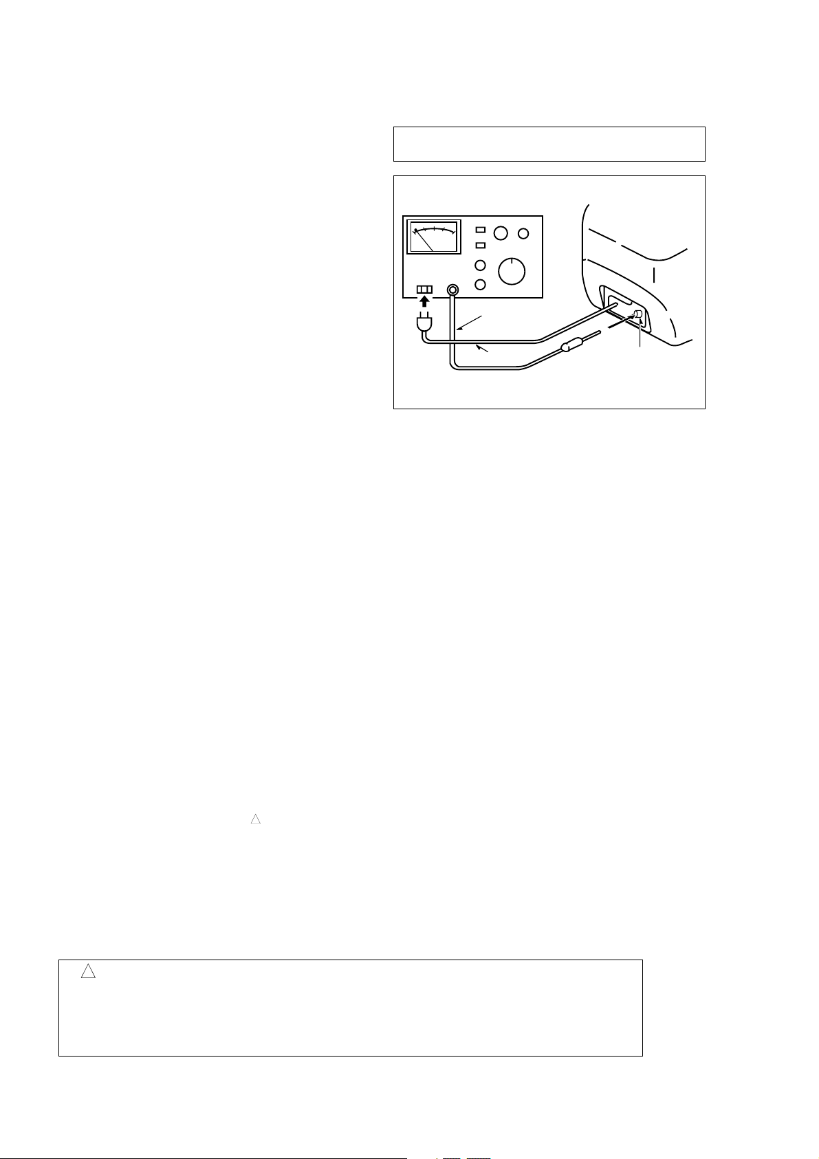
5. After repairing, always measure the insulation
resistance and perform the voltage-withstand test
(See Fig-1).
1) The insulation resistance must be 6.0 to 10 MΩ
when applying
2) In the voltage withstand test, apply 1.0 KV for 1
minute and check that the GO lamp lights.
500V per second.
Insulation resistance: 6.0 to 10 MΩ (500 V/s)
Voltage-withstand: 1.0 KV for 1 minute
Safety checker (Model 7110, etc.)
Earth cable
AC cable
Fig-1
Connect the earth cable
to the outside metal part
terminal.
* Breaking current set to 10 mA.
* Connect the safety checker as shown in Fig-1,
then measure the resistance and perform the test.
* Do not touch the equipment during testing.
* For details of the safety checker, refer to the supplied
Operation manual.
When servicing and checking on the TV, note the followings.
1. Keep the notices.
As for the places which need special attentions, they
are indicated with labels or seals on the cabinet,
chassis and parts. Make sure to keep the indications
and notices in the operation manual.
2. Avoid an electric shock.
There is a high voltage part inside. Avoid an electric
shock while the electric current is flowing.
3. Use the designated parts.
The parts in this equipment have the specific
characteristics of incombustibility and withstand
voltage for safety.
Therefore, use a part which has the same character
as the replaced part. Especially as to the important
parts for safety which is indicated in the circuit
diagram or the table of parts with a mark, the
designated parts must be used.
4. Put parts and wires in the original position after
assembling or wiring.
There are parts which use the insulation material
such as a tube or tape for safety, or which are
assembled so that these parts do not make contact
with the printed board. The inside wiring is designed
!
not to get close to the pyrogenic parts and high
voltage parts. Therefore, put these parts in the
original positions.
5. Take care of the cathode-ray tube.
By setting an explosion-proof cathode-ray tube in this
equipment, safety is secured against implosion.
However, when removing it or servicing from the
back, it gives out shock that is dangerous. Take
enough care to deal with it.
6. Avoid an X-ray.
Safety is secured against an X-ray by giving
considerations to the cathode-ray tube and the high
voltage peripheral circuit, etc. Therefore, when
repairing the high voltage peripheral circuit, use the
designated parts and do not change the circuit.
Repairing, except indicates, causes rising of high
voltage, and the cathode-ray tube emits an X-ray.
7. Perform a safety check after servicing.
Confirm that the screws, parts and wiring which were
removed in order to service are put in the original
positions, or whether there are deteriorated portions
around the places serviced.
!
Safety Components Symbol
This symbol is given to important parts which serve to maintain the safety of the product, and which
are made to confirm to special Safety Specifications.
Therefore, when replacing a component with this symbol make absolutely sure that you use a
designated part.
– 3 –
Page 4

ELECTRICAL MAIN PARTS LIST
REF. NO.
IC
8A-JEH-651-010 IC,TMP87CP38N
87-A21-133-080 IC,BMR-0101D
87-A91-538-010 RCR UNIT,SBX1981-72P
87-A21-433-010 IC,KS24C041I
87-A21-165-010 IC,TB1240AN
87-A21-166-010 IC,TA1275AZ
87-A21-259-010 IC,MM1454XD
87-A21-345-010 IC,NJM2150
87-A20-312-010 IC,M62420SP
87-A21-299-010 IC,LA6458SLL
87-A21-169-010 IC,MM1124B
87-A21-283-010 IC,AN5277
87-070-237-010 IC,LA7832
87-A21-344-010 IC,STR-F6656
87-020-903-010 IC,NJM7805FA
87-A20-389-010 IC,NJM7809FA
87-027-666-010 IC,TC4052BP
TRANSISTOR
87-A30-066-080 TR,2SA1175FE
87-A30-090-080 FET,2SK2541
87-A30-091-080 FET,2SJ460
89-337-794-580 TR,2SC3779 D/E
87-A30-065-080 TR,2SC2785FE
89-109-504-080 TR,2SA950Y
87-026-218-080 TR,DTC144ES (0.2W)
87-A30-121-080 TR,DTC 323 TS
87-A30-005-010 TR,2SC2688M/L
87-A30-095-010 TR,2SD2333LS
89-334-674-580 TR,2SC3467 D/E
87-A30-041-110 TR,SE115N
89-110-155-080 TR,2SA1015GR
DIODE
87-070-345-080 DIODE,IN4148
87-A40-347-080 ZENER MTZJ2.2B
87-070-444-080 ZENER,HZS33-1
87-A40-235-080 ZENER,MTZJ9.1C
87-A40-350-080 ZENER,MTZJ 4.7C
87-070-092-080 DIODE,S5566B
87-A40-286-080 DIODE,RGP10JE-5025
87-A40-794-080 DIODE,EGP20G
87-017-654-060 DIODE,GBU6J
87-A40-509-080 ZENER,MTZJ6.8C
87-A40-450-090 DIODE,RU 1P
87-A40-354-090 DIODE,UF3GL-6251
87-A40-611-080 ZENER,MTZJ3.9B
MAIN C.B
C1 87-018-151-080 CAP, TC U 20P-50V
C2 87-A11-073-080 CAP, TC U 22P-50V
C3 87-010-405-080 CAP, ELECT 10-50V
C4 87-018-134-080 CAPACITOR,TC-U 0.01-16
C5 87-010-263-080 CAP, ELECT 100-10 M
C6 87-018-119-080 CAP, CER 100P-50V
C7 87-010-405-080 CAP, ELECT 10-50V
C8 87-010-405-080 CAP, ELECT 10-50V
C9 87-018-134-080 CAPACITOR,TC-U 0.01-16
C10 87-018-119-080 CAP, CER 100P-50V
C11 87-018-119-080 CAP, CER 100P-50V
C13 87-010-405-080 CAP, ELECT 10-50V
C14 87-018-129-080 CAP,TC-U 680P-50 K B
C15 87-018-149-080 CAP,TC-U 15P-50 CH
C16 87-018-149-080 CAP,TC-U 15P-50 CH
C17 87-010-404-080 CAP, ELECT 4.7-50V
PART NO. DESCRIPTIONREF. NO. KANRI
KANRI
NO.
DESCRIPTION
PART NO.
NO.
C101 87-010-404-080 CAP, ELECT 4.7-50V
C102 87-018-134-080 CAPACITOR,TC-U 0.01-16
C103 87-010-384-080 CAP, ELECT 100-25V
C104 87-018-134-080 CAPACITOR,TC-U 0.01-16
C105 87-010-384-080 CAP, E 100-25 SME
C106 87-A10-207-080 CAP,TCS 0.01-50KBUP050
C107 87-018-134-080 CAPACITOR,TC-U 0.01-16
C108 87-018-132-080 CAP, CER 2200P-16V
C110 87-018-132-080 CAP, CER 2200P-16V
C113 87-010-260-080 CAP, ELECT 47-25V
C114 87-018-113-080 CAP, CER 33P-50V
C115 87-018-119-080 CAP, CER 100P-50V
C120 87-010-405-080 CAP, ELECT 10-50V
C121 87-018-134-080 CAPACITOR,TC-U 0.01-16
C122 87-010-260-080 CAP, ELECT 47-25V
C124 87-010-401-080 CAP, ELECT 1-50V
C125 87-018-134-080 CAPACITOR,TC-U 0.01-16
C126 87-010-544-080 CAP, ELECT 0.1-50V
C127 87-018-119-080 CAP, CER 100P-50V
C128 87-018-134-080 CAPACITOR,TC-U 0.01-16
C129 87-018-134-080 CAPACITOR,TC-U 0.01-16
C130 87-010-405-080 CAP, ELECT 10-50V
C131 87-010-405-080 CAP, ELECT 10-50V
C132 87-010-260-080 CAP, ELECT 47-25V
C134 87-018-134-080 CAPACITOR,TC-U 0.01-16
C135 87-018-132-080 CAP, TC U 2200P-16V
C136 87-018-132-080 CAP, TC U 2200P-16V
C301 87-010-545-080 CAP, ELECT 0.22-50V
C302 87-018-132-080 CAP, CER 2200P-16V
C303 87-018-148-080 CAP,TC-U 12P-50 CH
C307 87-018-134-080 CAPACITOR,TC-U 0.01-16
C308 87-010-385-080 CAP, ELECT 220-25 M
C309 87-018-147-080 CAP,TC-U 10P-50 CH
C310 87-018-147-080 CAP,TC-U 10P-50 CH
C311 87-018-147-080 CAP,TC-U 10P-50 CH
C312 87-010-404-080 CAP, ELECT 4.7-50V
C313 87-018-119-080 CAP, CER 100P-50V
C314 87-010-401-080 CAP, ELECT 1-50V
C315 87-018-196-080 CAP, CER 1500P-16V
C316 87-010-400-080 CAP, ELECT 0.47-50V
C317 87-010-381-080 CAP, ELECT 330-16 M
C318 87-018-134-080 CAPACITOR,TC-U 0.01-16
C319 87-010-400-080 CAP, ELECT 0.47-50V
C320 87-010-384-080 CAP, ELECT 100-25V
C321 87-018-134-080 CAPACITOR,TC-U 0.01-16
C323 87-018-209-080 CAP, CER 0.1-50V
C324 87-018-209-080 CAP, CER 0.1-50V
C328 87-010-400-080 CAP, ELECT 0.47-50V
C330 87-018-134-080 CAPACITOR,TC-U 0.01-16
C333 87-018-134-080 CAPACITOR,TC-U 0.01-16
C334 87-010-263-080 CAP, ELECT 100-10V
C335 87-010-401-080 CAP, ELECT 1-50V
C336 87-018-134-080 CAPACITOR,TC-U 0.01-16
C337 87-010-401-080 CAP, ELECT 1-50V
C338 87-010-401-080 CAP, ELECT 1-50V
C339 87-010-263-080 CAP, ELECT 100-10V
C340 87-018-134-080 CAPACITOR,TC-U 0.01-16
C341 87-018-134-080 CAPACITOR,TC-U 0.01-16
C344 87-010-263-080 CAP, ELECT 100-10V
C501 87-018-195-080 CAP, CER 1200P-16V
C502 87-018-115-080 CAP, CER 47P-50V
C503 87-010-247-080 CAP, ELECT 100-50V
C509 87-010-405-080 CAP, ELECT 10-50V
C510 87-010-401-080 CAP, ELECT 1-50V
C512 87-A10-011-090 CAP,E 2200-25 SMG
C513 87-018-127-080 CAP, CER 470P-50V
C601 87-A10-406-010 CAP,CER 270P-2K K BN DE
C603 87-A12-023-080 CAP,E 10-250 M SME
C606 87-016-515-080 CAP,CER 1000P-1K B
C607 87-010-397-090 CAP,E 1000-35 SME
– 4 –
Page 5

PART NO.
DESCRIPTIONREF. NO. KANRI
NO.
C609 87-010-386-080 CAP,E330-25 SME
C610 87-016-217-080 CAP,E 4.7-160
C611 87-A10-043-010 CAP,PP 0.56-200 PH
C613 87-A10-625-090 CAP,M/P 0.0082-1250 J
C614 87-012-396-090 CAP,CER 820P-2K K BN DE
C616 87-018-132-080 CAP, CER 2200P-16V
C617 87-010-976-080 CAP,CER 1000P-500 B
!
C618 87-010-974-080 CAP,CER 220P-500 B
!
C801 87-A10-688-090 CAP,M/P 0.22-275 K (B81133)
!
C802 87-A10-688-090 CAP,M/P 0.22-275 K (B81133)
!
C805 87-012-370-010 CAP,CER 3300P-250NS
C807 87-A10-646-090 CAP,E 220-400 SMH (25.4*40)
C808 87-A10-684-010 CAP,CER 680P-2K K BN DE
C809 87-018-131-080 CAP, CER 1000P-50V
C810 87-010-384-080 CAP, ELECT 100-25V
C811 87-018-127-080 CAP, CER 470P-50V
C812 87-018-129-080 CAP, CER 680P-50V
C813 87-A10-626-090 CAP,M/P 0.01-1250 J
C815 87-A11-779-090 CAP,M/P 1000P-1.6K J ECWH(VB)
C816 87-A10-867-090 CAP,CER 2200P-2K K R
C817 87-A10-731-090 CAP,E 220-160 M KMF
C818 87-016-221-090 CAP,E 100-160 M TWSS
C822 87-A10-832-080 CAP,CER 1000P-1K
C823 87-010-398-090 CAP,E 2200-35V
C824 87-A12-082-090 CAP,E 1000-35 SMG
C826 87-010-235-080 CAP,E 470-16 SME
C827 87-010-405-080 CAP, ELECT 10-50V
C828 87-010-405-080 CAP, ELECT 10-50V
C829 87-A10-469-080 CAP,CER 2200P-500 K B DD10
C830 87-010-405-080 CAP, ELECT 10-50V
C831 87-010-405-080 CAP, ELECT 10-50V
C832 87-010-405-080 CAP, ELECT 10-50V
C833 87-010-405-080 CAP, ELECT 10-50V
C834 87-010-382-080 CAP, E 22-25 SME
C835 87-010-384-080 CAP, E 100-25 SME
C901 87-010-405-080 CAP, ELECT 10-50V
C902 87-010-401-080 CAP, ELECT 1-50V
C903 87-010-401-080 CAP, ELECT 1-50V
C904 87-010-381-080 CAP, ELECT 330-16V
C905 87-010-405-080 CAP, ELECT 10-50V
C906 87-010-405-080 CAP, ELECT 10-50V
C907 87-010-405-080 CAP, ELECT 10-50V
C908 87-010-401-080 CAP, ELECT 1-50V
C909 87-010-401-080 CAP, ELECT 1-50V
C910 87-010-401-080 CAP, ELECT 1-50V
C911 87-010-401-080 CAP, ELECT 1-50V
C912 87-010-260-080 CAP, ELECT 47-25 SME
C913 87-018-134-080 CAPACITOR,TC-U 0.01-16
C914 87-018-134-080 CAPACITOR,TC-U 0.01-16
C915 87-018-133-080 CAPACITOR,TC-U 4700P-16
C916 87-018-133-080 CAPACITOR,TC-U 4700P-16
CF202 87-008-578-080 FLTR,TPS6.5MB2
CF204 87-008-577-080 FLTR,TPS5.5MB2
CF207 87-008-575-080 FLTR,SFSH5.5MCB
CF208 87-008-576-080 FLTR,SFSH6.5MCB
CN1 87-099-407-010 CONN,7P EH V WHT
CN102 87-010-384-080 CAP, E 100-25 M SME
CN601 87-099-675-010 CONN,5P V V
CN602 87-A60-485-010 CONN,2P V LV GRA
CN801 87-099-674-010 CONN,2P VA V
!
!
CN802 82-481-649-010 CONN, 2P V VT-50P
CN901 87-049-469-010 CONN,4P V
CNA301 84-LB2-631-010 CONN ASSY,5P TN-4
CNA801 8Z-JB9-663-010 CONN ASSY,8P V AU PW 200
CNA802 8Z-JB4-658-010 CONN ASSY,5P MAIN-NK 20'/21'
CNA900 8Z-JBX-602-010 CONN ASSY,4P SP 205-0.5
CNA901 8Z-JB9-662-010 CONN ASSY,6P V AU L/R 300
CNA902 8Z-JB4-660-010 CONN ASSY,5P 401-481 AUDIO
CNA903 8Z-JB9-661-010 CONN ASSY,10P MAIN-AUDIO
D9 87-A40-422-010 LED,SLP-581D-51 Y-G/R
PART NO.
DESCRIPTIONREF. NO. KANRI
NO.
D801 87-A90-965-010 VRIS,TNR15G471K
F801 87-035-458-010 FUSE,4A 250V T W/C
!
FB1 87-003-320-080 F-BEAD,FBR07HA121NB
FB501 87-003-320-080 F-BEAD,FBR07HA121NB
FB601 87-003-320-080 F-BEAD,FBR07HA121NB
FB801 87-003-320-080 F-BEAD,FBR07HA121NB
FB802 87-003-320-080 F-BEAD,FBR07HA121NB
FB805 87-003-320-080 F-BEAD,FBR07HA121NB
FB806 87-003-320-080 F-BEAD,FBR07HA121NB
FC801 87-033-213-080 CLAMP, FUSE
!
FC802 87-033-213-080 CLAMP, FUSE
!
FR601 87-A00-063-060 RES, FUSE 2.2-1/2W J
FR602 87-A00-419-090 RES, FUSE 1-2W J
FR603 87-029-150-090 RES, FUSE 3.9-2W J
FR604 87-A00-055-060 RES, FUSE 2.2-2W J
FR606 87-A00-049-060 RES, FUSE 2.2K-1/2W J
HL9 84-LB3-216-010 HLDR,LED
J901 87-A60-324-110 JACK,PIN 6P Y-W-R W/SW
J902 87-A61-021-010 JACK,PIN 3P W/SW YKC21-5734
J903 87-A60-858-010 JACK,3.5 BLK ST 2 SW
JW807 87-018-134-080 CAP,TC U 0.01-16 N Y
L1 87-003-147-080 COIL, 22UH
L2 87-003-152-080 COIL, 100UH
L101 87-005-444-080 COIL 100UH,K
L102 87-003-152-080 COIL, 100UH
L104 87-003-097-080 COIL,1.0UH K LAL02
L106 87-003-282-080 COIL,12UH
L111 87-003-145-080 COIL,8.2UH
L112 87-003-149-080 COIL,47UH
L114 87-A50-530-010 COIL,VCO38.0MHZ
L301 87-005-444-080 COIL 100UH,K
L302 87-005-474-080 COIL,12UH J FLR50
L303 87-005-444-080 COIL 100UH,K
L601 87-A50-040-010 COIL,2.2MH
L602 88-JBJ-625-010 COIL,HLC-ELH5L4120N
L801 87-A50-170-010 COIL,390UH RCH106
!
LF801 87-JB8-651-010 FLTR,LINE SS24H-K15070
PR801 87-A90-090-080 PROTECTOR,1.5A 491SERIES 60V
!
PR803 87-A90-094-080 PROTECTOR,4A 491SERIES 60V
!
PR804 87-A90-094-080 PROTECTOR,4A 491SERIES 60V
!
!
PS801 87-A91-407-010 P-COUPLER,ON3171-R
PS802 87-A91-407-010 P-COUPLER,ON3171-R
!
PT801 8Z-JBA-621-010 PT,SW ZJB-KE-7 M
!
R101 87-A00-164-090 RES,M/F 12K-2W J RSF(S)
R123 87-010-260-080 CAP,E 47-25 M
R511 87-025-119-090 RES,M/F 560-1W J
R612 87-A00-225-090 RES,M/F 2.2K-5W J
R619 87-A00-200-090 RES,M/F 100-2W J
R802 87-A00-552-010 RES,CEM 1.0-10W J MPC722
R803 87-A00-552-010 RES,CEM 1.0-10W J MPC722
R804 87-A00-543-080 RES,SD 8.2M-1W J RCR60
R807 87-A00-639-090 RES,CEM 0.15-5W K BPR
R808 87-A00-573-090 RES,CEM 0.33-5W K BPR
R816 87-A00-170-090 RES,M/F 82K-3W J RSF(S)
R817 87-A00-223-090 RES,M/F 47K-2W J RSF(S)
R827 87-A00-673-090 RES,M/F 82K-5W J RSS5L30
R830 87-A00-158-090 RES,M/F 15-2W J RSF(S)
R936 87-A00-070-090 RES,M/F 220-1W J
R937 87-A00-070-090 RES,M/F 220-1W J
S1 87-A90-712-080 SW,TACT EVQ11L07K
S2 87-A90-712-080 SW,TACT EVQ11L07K
S3 87-A90-712-080 SW,TACT EVQ11L07K
S4 87-A90-712-080 SW,TACT EVQ11L07K
S5 87-A90-712-080 SW,TACT EVQ11L07K
S6 87-A90-712-080 SW,TACT EVQ11L07K
S501 87-A90-567-010 SW,LVR 4-1-3 EVQRAAL10
!
S801 87-A91-410-010 SW,AC PUSH 1-1-1 ESB92SH1B
SWF202 87-A90-337-010 FLTR,SAW OFW-K2959M
T601 8Z-JBR-605-010 FBT, HFT3607(SAN)21-C
!
T602 84-LB3-651-010 TRANS,HD MS-101N
!
– 5 –
Page 6

PART NO.
DESCRIPTIONREF. NO. KANRI
NO.
THP801 87-A90-759-010 POS-THMS,PTH451C272BF300N270
!
TU101 87-A91-495-010 TU UNIT, ENV59D58G3-38.0MHZ
X1 87-030-300-080 VIB,XTAL 8.00MHZ
X301 87-A70-054-080 VIB,XTAL 4.43MHZ AQC-1018
AUDIO C.B
C401 87-010-402-080 CAP, ELECT 2.2-50V
C402 87-010-260-080 CAP, ELECT 47-25V
C403 87-018-134-080 CAPACITOR,TC-U 0.01-16
C405 87-010-402-080 CAP, ELECT 2.2-50V
C406 87-010-405-080 CAP, ELECT 10-50V
C407 87-A11-148-080 CAP,TC U 0.1-50 Z F
C408 87-010-367-080 CAP,E 4.7-25 BP
C411 87-010-367-080 CAP,E 4.7-25 BP
C412 87-010-405-080 CAP, ELECT 10-50V
C413 87-A11-148-080 CAP,TC U 0.1-50 Z F
C414 87-010-405-080 CAP, ELECT 10-50V
C415 87-010-367-080 CAP,E 4.7-25 BP
C418 87-010-367-080 CAP,E 4.7-25 BP
C419 87-A11-148-080 CAP,TC U 0.1-50 Z F
C420 87-010-260-080 CAP, ELECT 47-25V
C421 87-010-260-080 CAP, ELECT 47-25V
C422 87-018-134-080 CAPACITOR,TC-U 0.01-16
C426 87-A11-148-080 CAP,TC U 0.1-50 Z F
C427 87-010-401-080 CAP, ELECT 1-50V
C428 87-018-134-080 CAPACITOR,TC-U 0.01-16
C429 87-010-263-080 CAP, ELECT 100-10V
C433 87-A11-148-080 CAP,TC U 0.1-50 Z F
C434 87-A11-148-080 CAP,TC U 0.1-50 Z F
C435 87-010-260-080 CAP, ELECT 47-25V
C436 87-018-119-080 CAP, CER 100P-50V
C437 87-018-119-080 CAP, CER 100P-50V
C438 87-010-367-080 CAP,E 4.7-25 BP
C440 87-A11-147-080 CAP,TC U 0.047-50 Z F
C442 87-A11-147-080 CAP,TC U 0.047-50 Z F
C445 87-010-367-080 CAP,E 4.7-25 BP
C446 87-010-101-080 CAP, ELECT 220-16
C447 87-A11-148-080 CAP,TC U 0.1-50 Z F
C467 87-010-367-080 CAP,E 4.7-25 BP
C470 87-010-112-080 CAP, ELECT 100-16V
C471 87-A11-148-080 CAP,TC U 0.1-50 Z F
C472 87-010-367-080 CAP,E 4.7-25 BP
C475 87-010-379-080 CAP, ELECT 22-16V
C476 87-010-400-080 CAP, ELECT 0.47-50V
C477 87-010-400-080 CAP, ELECT 0.47-50V
C478 87-010-401-080 CAP, ELECT 1-50V
PART NO.
DESCRIPTIONREF. NO. KANRI
NO.
C479 87-010-247-080 CAP, ELECT 100-50V
C480 87-010-388-080 CAP ELECT 1000-25V SME
C481 87-010-388-080 CAP ELECT 1000-25V SME
C482 87-010-401-080 CAP, ELECT 1-50V
C483 87-010-247-080 CAP, ELECT 100-50V
C484 87-A11-148-080 CAP,TC U 0.1-50 Z F
C493 87-010-112-080 CAP, ELECT 100-16V
C498 87-010-402-080 CAP, ELECT 2.2-50 SME
CN401 87-009-034-010 CONN,6P PH V
CN402 87-009-038-010 CONN,10P V WHT
CN403 87-099-408-010 CONN,8P EH V WHT
CN404 87-009-195-010 CONN,5P B5BEH
FR996 87-A00-084-090 RES,FUSE 1-1W J
FR997 87-A00-084-090 RES,FUSE 1-1W J
R401 87-025-381-080 RES,M/F 18K-1/6W F
R402 87-025-424-080 RES,M/F 10K 1/6W F
R404 87-025-380-080 RES,M/F 15K-1/6W F
R405 87-025-381-080 RES,M/F 18K-1/6W F
NK C.B
!
C551 87-010-976-080 CAP,CER 1000P-500 B
C552 87-012-397-010 CAP,CER 1000P-2K BN
!
C553 87-018-127-080 CAP,TC-U 470P-50
C554 87-018-127-080 CAP,TC-U 470P-50
C555 87-018-128-080 CAP,TC-U 560P-50 B
C556 87-010-405-080 CAP, ELECT 10-50V
C557 87-010-405-080 CAP, ELECT 10-50V
CN551 87-009-195-010 CONN,5P B5BEH
CN552 87-049-590-010 CONN,5P 8283 V WHT
CN553 87-A61-112-080 CONN,1P V BLU TP00704
CN554 87-A61-060-080 CONN,1P V RED TP00706
L551 87-005-444-080 COIL 100UH,K
R551 87-A00-165-090 RES,M/F 15K-2W J RSF(S)
R552 87-A00-165-090 RES,M/F 15K-2W J RSF(S)
R553 87-A00-165-090 RES,M/F 15K-2W J RSF(S)
SO552 86-LBR-670-010 SOCKET,CRT 9P HPS1521
KEY C.B
JOINT.F C.B
JOINT.R C.B
– 6 –
Page 7
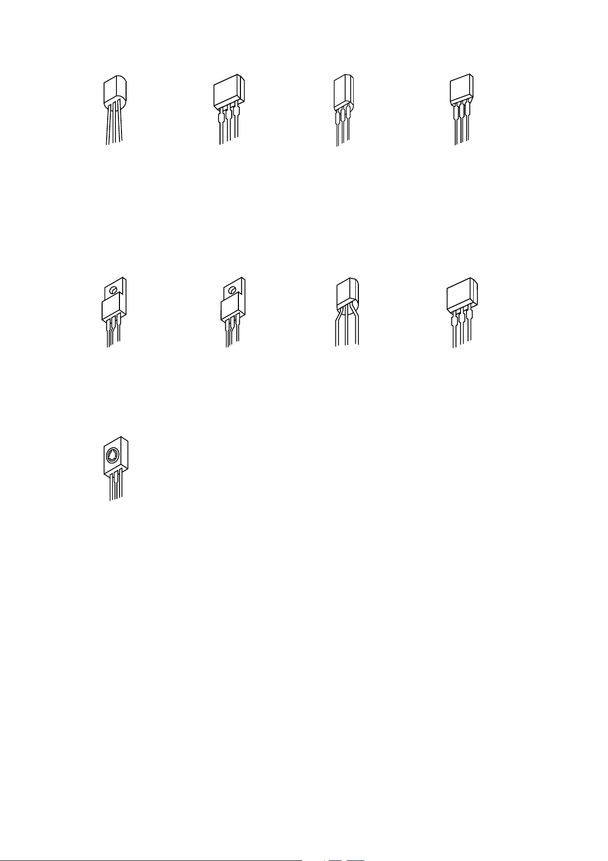
TRANSISTOR ILLUSTRATION
E C B
2SA950
2SA1015
B C E
S D G
2SJ460
2SK2541
1 2 3
SE115N
1. SENSE
2. COLLECTOR
3. GROUND
E C B
2SC3467
E C B
2SC3779
E C B
2SA1175
2SC2785
DTC144ES
E C B
DTC3232SD2333
E C B
2SC2688
– 7 –
Page 8
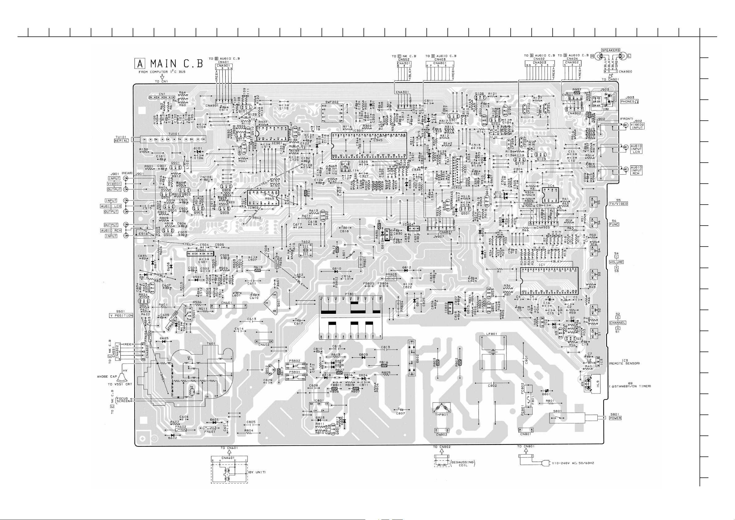
WIRING - 1 (MAIN)
101112131415161718192021222324
1234567892526272829303132
A
B
C
D
E
F
G
H
I
J
K
L
M
N
O
P
Q
– 8 –
R
S
T
U
Page 9
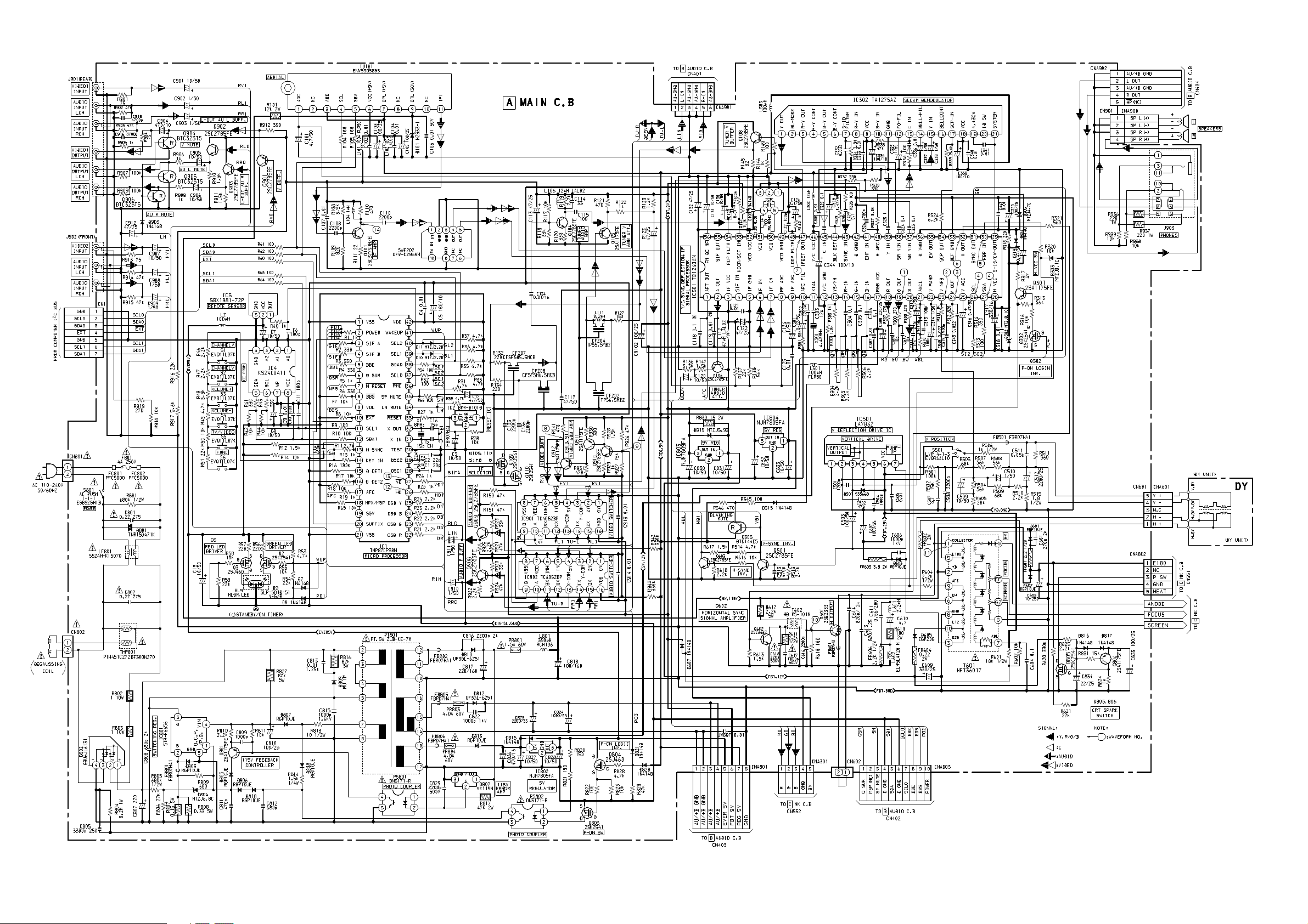
SCHEMATIC DIAGRAM - 1 (MAIN)
– 9 –
Page 10

WIRING - 2 (AUDIO)
101112131415161718192021222324
1234567892526272829303132
A
B
C
D
E
F
G
H
I
J
K
L
M
N
O
P
Q
– 10 –
R
S
T
U
Page 11

SCHEMATIC DIAGRAM - 2 (AUDIO)
– 11 –
Page 12

WIRING - 3 (NK)
123456789101112131415
A
B
C
D
E
F
G
H
I
J
K
L
M
N
O
P
Q
– 12 –
R
S
T
U
Page 13

SCHEMATIC DIAGRAM - 3 (NK)
– 13 –
Page 14

IC BLOCK DIAGRAM
– 14 –
Page 15

– 15 –
Page 16

IC DESCRIPTION
IC, TMP87CP38N
Pin No. Pin Name I/O Description
1 VSS – Connected to GND.
2 POWER O During standby mode, "H" level is inserted to switch off H deflection & high voltage.
3 SIF A O SOUND IF switch A.
4 SIF B O SOUND IF switch B.
5 BBE O BBE select.
6 Q SUR O Q SURROUND switch.
7 N RESET O NICAM RESET ("L" = reset).
8 BBS O BASS BOOST / S-WOOFER.
9 VOL
–
10 EXT I External bus switch.
11 SCL1 O I
12 SDA1 I/O I2C bus CH1 data.
13 H SYNC I Sync signal input pin for detection.
14 KEY IN I Input key is detected by monitor.
15 D DET1 I Power condition 1 (mid = good, low/high = bad).
Not used.
2
C bus CH1 clock.
16 D DET2 I Power condition 2 (mid = good, low/high = bad).
17 AFC I AFT voltage input pin.
18 MPX/MSP I MPX detect / MSP key in. (Connected to VDD through a resistor)
19 SGV O Test signal output when test mode. (Not used)
20 SUFFIX I Feature select (initial) input.
21 VSS – Connected to GND.
22 OSD R O OSD red output.
23 OSD G O OSD green output.
24 OSD B O OSD blue output.
25 OSD Y O OSD blanking signal output.
26 HD I OSD horizontal synchronised signal input.
27 VD I OSD vertical synchronised signal input.
28 OSC1 – Connected to OSC coil.
29 OSC2 – Connected to OSCcoil.
30 TEST – Connected to GND.
31 X IN I 8 MHz clock input.
32 X OUT O 8 MHz clock output.
33 RESET I Use to reset the micon when power up.
34 LN MUTE O "H" to mute the line out signal.
35 SP MUTE O "H" to mute the audio signal.
36 RMC I Remote control signal is led to this pin.
37 SCL0 I I
38 SDA0 I/O I
2
C bus CH2 clock.
2
C bus CH2 data.
39 SEL1 O Input select switch 1.
40 SEL2 O Input select switch 2.
41 WAKEUP O LED (wakeup timer).
42 VDD – 5V supply.
– 16 –
Page 17

IC, TB1240AN
Pin No. Pin Name I/O Description
1 AFT OUT O The terminal for AFT output and self-adjust output.
2 A OUT O
3 IF VCC – VCC of PIF circuit.
4 SIF IN I SIF input pin. (Not used)
5 IF GND – GND of PIF circuit.
6 IF IN I IF signal input.
7 IF IN I IF signal input.
8 RF AGC O RF AGC output.
9 IF AGC – The terminal to be connected with an IF AGC filter.
10 APC FIL – APC filter of chroma for demodulation.
11 XTAL I 4.43MHz crystal oscillator.
12 Y/C GND – GND of Y/C circuit.
13 YS/YM I The terminal for switching of analog RGB mode and fast half tone.
14 R-IN I Analog red signals input.
15 G-IN I Analog green signals input.
16 B-IN I Analog blue signals input.
17 RGB VCC – VCC of RGB circuit.
18 R OUT O R signals output.
19 G OUT O G signals output.
Audio output pin.
20 B OUT O B signals output.
21 ABCL I ABL/ACL control.
22 V RAMP – Connected with cap to make Vertical RAMP signal.
23 V NFB I Input of Vertical sawteeth signal feedback.
24 V OUT O Vertical drive signal output.
25 V AGC – Vertical AGC cap.
26 SCL I I
27 SDA I/O I2C bus data input/output.
28 H VCC – VCC of vertical circuit.
29 S-ID/CW OUT I/O SECAM ID input and PAL/NTSC ID output.
30 FBP IN I FBP input.
31 SYNC OUT O Composites sync output.
32 H OUT O Horizontal drive signal output.
33 DEF GND – GND of deflection circuit.
34 SCP OUT O Sand castle pulse (VD+HD+GP) output.
35 EW OUT O E-W output. (Not used)
36 D VDD – VDD of digital block.
37 SB YIN I B-Y signals input.
2
C bus clock input.
38 SR YIN I R-Y signals input.
39 Y IN I Y signal input.
40 H AFC – H.AFC filter.
41 EHT IN I The terminal for EHT. (Not used)
42 D GND – GND of digital block.
– 17 –
Page 18

Pin No. Pin Name I/O Description
43 SYNC IN I Input of the synchronous separation circuit.
44 BLK DET – The terminal to be connected with an Black Det filter.
45 C IN I Input of chroma signals.
46 Y/C VCC – VCC of Y/C circuit.
47 IFDET OUT O Composite video signal and SIF signal detected in IF circuit.
48 LOOP FLTR – Loop filter for IF PLL.
49 VCO GND – GND of VCO and SIF circuit.
50 VCO – The terminal connected with a tank coil for IF VCO.
51 VCO – The terminal connected with a tank coil for IF VCO.
52 VCO VCC – VCC of IF VCO and SIF.
53 HCOR/SIF IN I H.curve correction and SIF input.
54 RIP FLTR – Connected with cap to stabilize the performance of SIF injection-lock circuit.
55 SIF OUT O Output of 2nd SIF signal. (Not used)
56 FM DC NF I The terminal for FM DC negative feedback and AGC filter for L-SECAM.
IC, TA1275AZ
Pin No. Pin Name I/O Description
1 Y OUT O The output pin for Y signal.
The pin for controlling the Y processing mode:
2 DL-MODE O
3 R-Y OUT O The output pin for demodulated R-Y signal.
4 R-Y CONT I The pin for controlling the black offset level. (Not used)
5 B-Y OUT O The output pin for demodulated B-Y signal.
6 B-Y CONT I The pin for controlling the black offset level. (Not used)
7 S-ID FILTER I The pin for connecting the SECAM ident filter capacitor.
8 R-Y IN I The input pin for external R-Y signal. (Not used)
9 VCC – The VCC pin for Y/C processing block.
10 B-Y IN I The input pin for external B-Y signal. (Not used)
11 GND – The GND pin.
12 F0-FIL I The pin for connecting a capacitor for automatic adjusting circuit.
13 C IN I The chroma signal input pin.
14 BELL-FIL I The pin for connecting a capacitor for the bell filter fo, 4.286MHz.
15 Y IN I The Y signal input pin.
16 BELLCONT I
17 SCP-IN I The pin to input the sand castle pulse, SCP.
18 VCC – VCC pin for logic block.
to VCC: 5.5MHz trap ; open: 5.5MHz trap + D.L ; to GND: DL. (Not used)
The pin for selecting the bell filter fo. fo + 70KHz: open ;
fo + 35KHz:20k to GND ; fo: to GND. (Connected to GND).
19 4.43 CW I The pin for input 4.43MHz of carrier wave for self adjustment circuit.
20 ID SW I
21 SYSTEM I/O The interface pin to the main processor.
The switch pin for selecting the ID detection mode. H + V: connected to VCC ;
Auto search: opened ; H: connected to GND. (Not used.)
– 18 –
Page 19

VOLTAGE CHART
REF NO. S D G
Q2 0.2 5.1 1.0
REF NO. S D G
Q3 5.1 1.2 4.1
REF NO. E C B
Q101 1.2 0.5 8.9
REF NO. E C B
Q104 1.6 9.0 2.2
REF NO. E C B
Q105 3.6 0.0 2.9
REF NO. E C B
Q106 3.6 9.0 4.2
REF NO. E C B
Q404 0.2 0.2 0.3
REF NO. E C B
Q407 0.2 0.2 0.0
REF NO. S D G
Q408 0.0 11.1 0.2
REF NO. S D G
Q409 0.2 0.2 4.8
REF NO. E C B
Q414 8.9 0.0 9.1
REF NO. E C B
Q501 0.0 4.5 0.2
REF NO. E C B
Q108 2.9 9.0 3.6
REF NO. S D G
Q109 0.0 0.8 0.0
REF NO. S D G
Q110 0.0 0.0 5.1
REF NO. E C B
Q301 11.3 11.2 10.6
REF NO. S D G
Q302 0.0 0.0 4.7
REF NO. E C B
Q303 0.0 0.3 4.5
REF NO. E C B
Q554 2.0 0.0 1.3
REF NO. E C B
Q551 2.8 139.0 3.0
REF NO. E C B
Q552 2.7 141.1 3.0
REF NO. E C B
Q553 2.6 145.1 2.9
REF NO. E C B
Q601 0.0 - *
REF NO. E C B
Q602 0.0 63.2 0.4
REF NO. E C B
Q401 0.2 2.3 0.2
REF NO. E C B
Q402 0.2 3.2 0.1
REF NO. E C B
Q603 0.0 4.2 0.0
REF NO. E C B
Q801 15.2 0.6 14.7
* Refer to Waveform no. 10
– 19 –
Page 20

REF NO. 1 2 3
Q802 114.7 92.5 0.0
REF NO. E C B
Q911 7.4 2.4 6.8
REF NO. S D G
Q803 0.0 0.1 4.5
REF NO. S D G
Q804 4.5 5.1 4.6
REF NO. S D G
Q805 0.0 8.9 0.0
REF NO. E C B
Q806 4.8 0.0 5.7
REF NO. E C B
Q901 2.5 0.0 1.8
REF NO. E C B
Q902 0.0 9.0 0.9
REF NO. E C B
Q903 0.0 9.0 0.8
REF NO. E C B
Q912 1.8 9.0 2.4
IC1, TMP87CP38N
PIN NO. VOLT (V)
1 0.0
2~3 5.1
4 0.0
5 0.0
6 5.1
7~9 0.0
10~12 5.1
13 4.6
14 5.1
15 0.0
16 2.6
17 2.2
18 5.1
REF NO. E C B
Q904 0.0 2.5 0.1
REF NO. E C B
Q905 0.0 0.0 0.1
REF NO. E C B
Q906 0.0 0.0 0.1
REF NO. E C B
Q908 0.9 8.9 1.4
REF NO. E C B
Q909 0.8 8.9 1.4
REF NO. E C B
Q910 1.5 6.8 2.1
19 0.0
20 0.7
21~25 0.0
26 4.2
27 4.5
28~29 5.1
30 0.0
31 2.2
32 2.5
33 5.1
34~35 0.1
36 5.1
37~38 5.0
39~40 5.1
41 0.1
42 5.1
– 20 –
Page 21

IC2, BMR-0101D
PIN NO. VOLT (V)
1 5.1
2 0.0
3 0.1
IC301, TB1240AN
PIN NO. VOLT (V)
17 9.0
18 3.0
19 2.9
20 2.8
IC302, TA1275AZ
PIN NO. VOLT (V)
1 2.9
2 2.1
3~6 2.6
7 2.1
IC3, SBX1981-72P
PIN NO. VOLT (V)
1 5.1
2 0.0
3 5.1
IC4, KS24C041I
PIN NO. VOLT (V)
1~4 0.0
5~6 5.1
7 0.0
8 5.1
IC301, TB1240AN
PIN NO. VOLT (V)
1 3.1
2 4.1
3 8.8
4 5.0
5 0.0
6 0.9
7 1.9
8 4.0
9 4.1
10 2.0
11 3.0
12 0.0
13 0.1
14~16 2.7
21 5.9
22 4.1
23 4.8
24 0.7
25 1.8
26 5.0
27 5.0
28 9.2
29 3.5
30 1.4
31 4.6
32 2.0
33 0.0
34 1.2
35 3.6
36 4.9
37 2.6
38 2.6
39 2.9
40 7.1
41 0.7
42 0.0
43 2.9
44 2.3
45 0.2
46 5.0
47 3.5
48 4.5
49 0.0
50 7.9
51 7.9
52 8.8
53 4.5
54 5.6
55 3.5
56 4.4
8 2.6
9 5.1
10 2.6
11 0.0
12 2.7
13 4.4
14 2.5
15 2.9
16 0.0
17 0.7
18 5.1
19 2.7
20 2.5
21 3.5
IC401, MM1454XD
PIN NO. VOLT (V)
1~2 4.3
3 4.9
4 0.3
5~7 4.3
8 0.2
9~13 4.3
14 5.0
15 4.3
16 9.2
IC402, NJM2150
PIN NO. VOLT (V)
1~7 4.7
8~11 0.2
12 9.1
13~20 4.7
– 21 –
Page 22

IC403, M62420SP
PIN NO. VOLT (V)
1 4.7
2~3 4.6
4 4.7
5~6 4.4
7 4.7
8 0.2
9~10 5.2
11~12 5.3
13 0.2
14 4.7
15 4.4
16 4.4
17 4.7
18~19 4.6
20 9.1
IC404, LA6458SLL
PIN NO. VOLT (V)
1 9.1
2-4 4.7
5 0.2
6~8 4.7
9 9.1
IC410, AN5277
PIN NO. VOLT (V)
1 0.0
2 0.2
3 23.1
4~5 0.2
6 0.0
7 11.4
8 0.8
9 0.0
10 24.3
11 11.1
12 11.6
IC501, LA7832
PIN NO. VOLT (V)
1 1.9
2 24.0
3 0.6
4 0.7
5 24.4
6 13.7
7 0.0
IC803, NJM7809FA
PIN NO. VOLT (V)
1 11.7
2 0.0
3 9.0
IC804, NJM7805FA
PIN NO. VOLT (V)
1 9.0
2 0.0
3 5.1
IC901, TC4052BP
PIN NO. VOLT (V)
1 0.0
2 0.1
3~4 2.2
5 0.1
6~8 0.0
9~10 6.6
11~15 0.0
16 9.1
IC409, MM1124B
PIN NO. VOLT (V)
1~2 4.7
3 4.6
4~6 4.7
7 0.8
8 0.2
9 0.3
10 0.0
11 4.7
12 4.6
13 4.7
14 4.6
15 4.7
16 9.1
IC801, STR-F6656
PIN NO. VOLT (V)
1 0.2
2 0.0
3 295.0
4 15.7
5 0.0
IC802, NJM7805FA
PIN NO. VOLT (V)
1 11.3
2 0.0
3 5.1
– 22 –
IC902, TC4052BP
PIN NO. VOLT (V)
1~2 0.0
3~4 4.1
5 5.0
6~8 0.0
9~10 6.6
11 4.1
12 0.0
13 4.1
14 5.0
15 0.0
16 9.1
Page 23

WAVEFORM
AC : 220V INPUT : TUNER PAL-COLOR BAR AUDIO 1kHz USER CONTROL : ALL RESET
MAIN C.B
IC301 PIN 19 (GOUT)
1
IC301 PIN 30 (FBP IN)
5
1
IC301 PIN 23 (V NFB)
2
2
IC301 PIN 24 (VOUT)
3
1 V/div
10 µs/div
1 V/div
5 ms/div
5
IC301 PIN 32 (H OUT)
6
6
IC301 PIN 47 (IF DET OUT)
7
2 V/div
20 µs/div
1 V/div
20 µs/div
3
IC301 PIN 26/27 (SCL/SDA)
4
4
0.2 V/div
5 ms/div
Pin 26
Pin 27
2 V/div
5 ms/div
– 23 –
7
Q912 EMITTER
8
8
1 V/div
20 µs/div
0.5 V/div
20 µs/div
Page 24

Q910 BASE
9
IC1 PIN27 (VD)
13
9
Q601 BASE
10
10
T601 PIN 1 (COLLECTOR)
11
0.5 V/div
20 µs/div
1 V/div
20 µs/div
13
14
Q101 COLLECTOR
14
AUDIO C.B
15
IC401 PIN 1 (RIN)
1 V/div
5 ms/div
0.1 V/div
20 µs/div
11
12
IC1 PIN 26 (HD)
12
20 V/div
20 µs/div
1V/div
20 µs/div
15
16
IC402 PIN 7 (OUTPUT (A))
16
1 V/div
500 µs/div
1 V/div
500 µs/div
– 24 –
Page 25

IC403 PIN 14 (OUT2)
17
IC410 PIN 7 (CH2 OUT)
19
17
18
IC409 PIN 15 (IN2)
18
1 V/div
500 µs/div
1 V/div
500 µs/div
19
NK C.B
20
Q552 COLLECTOR
20
2 V/div
500 µs/div
50 V/div
20 µs/div
– 25 –
Page 26

MECHANICAL EXPLODED VIEW 1 / 1
WIRE ASSY,
D
CRT GND 21
E
P.C.B
15
F
SPR-E,
EARTH
E
E
E
13
8
P.C.B
C
6
C
J
12
14
D
H
H
16
17
11
J
J
F
G
I
10
9
C
8
C
5
1
B
2
A
4
3
7
P.C.B
TV-A2115 KEJL6CM
(FileName:EXP.EPS)
125/1 AJB-K
– 26 –
Page 27

MECHANICAL PARTS LIST 1 / 1
PART NO.
1 87-054-087-010 BADGE,AIWA 40
2 8A-JBK-002-010 PANEL,MAIN A2115
3 8Z-JBR-005-010 LENS,RC
4 8Z-JBR-006-010 LENS,LED
5 8Z-JBR-004-010 KEY,MAIN
6 8A-JBG-001-010 CABI,FR BL
7 8Z-JB4-695-010 AC CORD SET,EH BLK
!
8 8Z-JB4-620-010 SPKR,6*12 8OHM 10W
9 8Z-JB5-007-010 BTN,POWER SH
10 84-LB3-216-010 HLDR,LED
11 8Z-JBX-602-010 CONN ASSY,4P SP 205-0.5
12 8Z-JBR-201-010 HLDR,PCB 1
!
13 86-LB2-603-010 CRT,A51LMV10X06N00
!
14 87-JBN-630-010 DGC,21PAL 7JB-22
15 8Z-JBR-012-010 CABI,REAR N
16 8Z-JB5-010-010 PANEL,REAR SH
17 87-A90-332-010 HLDR,SF-2001 HV CABLE
A 87-067-680-010 BVI T3+3-10
B 87-067-758-010 BVT2+3-12 W/O SLOT
C 87-078-070-010 BVIT3B+4-12
D 86-LBB-206-010 S-SCREW,ASSY TV5-40 W20
E 8Z-JBS-204-010 W-PVC,10-20-1
F 87-067-844-010 BVT2+4-16 BLK
G 87-067-690-010 TAPPING SCREW, BVIT3+3-12
H 87-067-761-010 TAPPING SCREW, BVT2+3-10
I 87-B10-090-010 BVIT3B+3-12 GOLD
J 87-067-579-010 TAPPING SCREW, BVT2+3-8
NO.
DESCRIPTIONREF. NO. KANRI
COLOR NAME TABLE
Basic color symbol Color Basic color symbol Color Basic color symbol Color
B Black C Cream D Orange
G Green H Gray L Blue
LT Transparent Blue N Gold P Pink
R Red S Silver ST Titan Silver
T Brown V Violet W White
WT Transparent White Y Yellow YT Transparent Yellow
LM Metallic Blue LL Light Blue GT Transparent Green
LD Dark Blue DT Transparent Orange GM Metallic Green
YM Metallic Yellow DM Metallic Orange
– 27 –
Page 28

2–11, IKENOHATA 1–CHOME, TAITO-KU, TOKYO 110, JAPAN TEL:03 (3827) 3111
Printed in Singapore9301978 0251431
 Loading...